

EIC BR3510, BR3501, BR3500, BR3508, BR3506 Datasheet
...
BR3500 - BR3510
FEATURES :
* High current capability
* High surge current capability
* High reliability
* Low reverse current
* Low forward voltage drop
* Ideal for printed circuit board
MECHANICAL DATA :
* Case : Molded plastic with heatsink integrally
mounted in the bridge encapsulation
* Epoxy : UL94V-O rate flame retardant
* Terminals : plated .25" (6.35 mm). Faston
* Polarity : Polarity symbols marked on case
* Mounting position : Bolt down on heat-sink with
silicone thermal compound between bridge
and mounting surface for maximum heat
transfer efficiency.
* Weight : 17.1 grams
MAXIMUM RATINGS AND ELECTRICAL CHARACTERISTICS
Rating at 25
°
C ambient temperature unless otherwise specified.
Single phase, half wave, 60 Hz, resistive or inductive load.
For capacitive load, derate current by 20%.
RθJC
1. Thermal Resistance from junction to case with units mounted on a 7.5" x 3.5" x 4.6" (19cm.x 9cm.x 11.8cm.) Al.-Finned Plate
UPDATE : APRIL 23, 1998
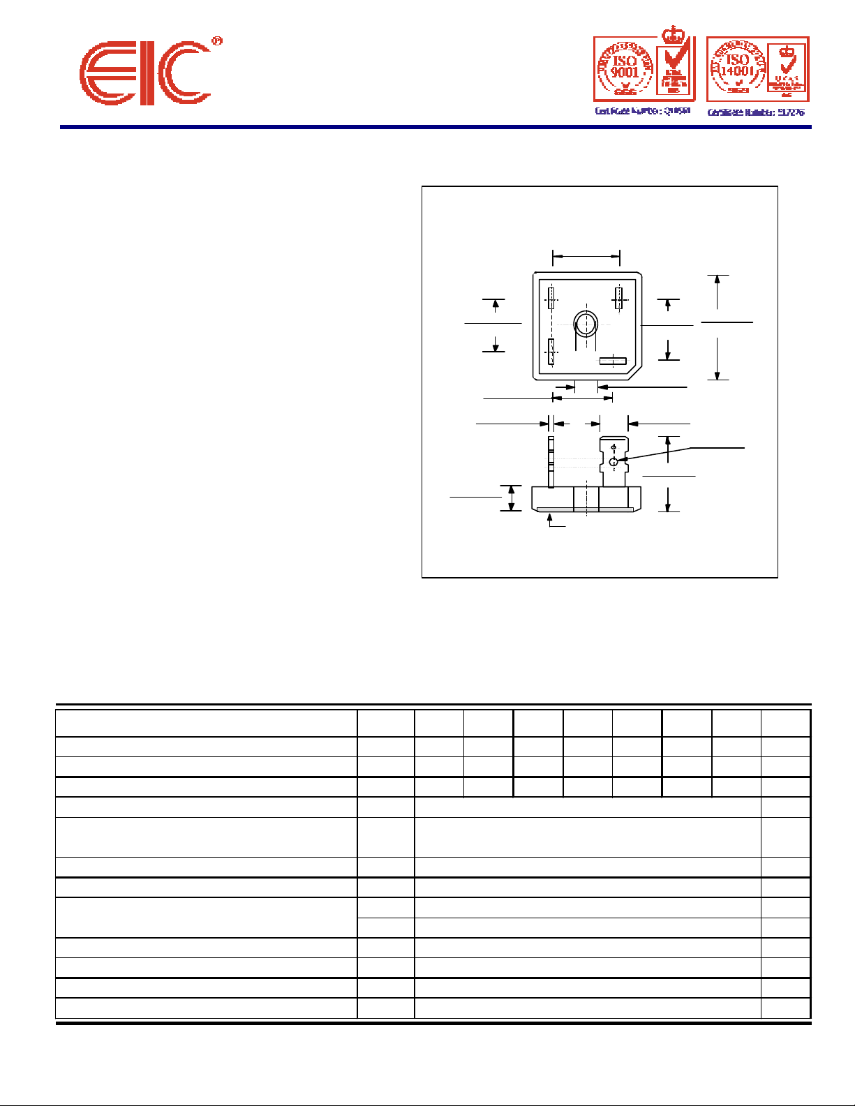
0.688(17.40)
0.530(13.40)
0.618(15.70)
1.120(28.40)
0.200(5.10)
0.618(15.70)
0.028(0.71)
0.280(7.11)
SILICON BRIDGE RECTIFIERS
PRV : 50 - 1000 Volts
Io : 35 Amperes
BR50
0.728(18.50)
0.570(14.50)
0.658(16.70)
0.032(0.81)
0.310(7.87)
Metal Heatsink
Dimensions in inches and ( millimeters )
0.685(16.70)
0.210(5.30)
0.252(6.40)
0.248(6.30)
φ
0.905(23.0)
0.826(21.0)
1.130(28.70)
0.100(2.50)
0.090(2.30)
RATING
Maximum Recurrent Peak Reverse Voltage
Maximum RMS Voltage V
Maximum DC Blocking Voltage VDC 50 100 200 400 600 800 1000 Volts
Maximum Average Forward Current Tc = 55°C
Peak Forward Surge Current Single half sine wave
Superimposed on rated load (JEDEC Method)
Current Squared Time at t < 8.3 ms.
Maximum Forward Voltage per Diode at IF = 17.5 Amp. VF 1.0 Volts
Maximum DC Reverse Current Ta = 25 °C
at Rated DC Blocking Voltage Ta = 100 °C
Typical Thermal Resistance (Note 1)
Typical Thermal Resistance at Junction to Ambient
Operating Junction Temperature Range TJ - 40 to + 150
Storage Temperature Range TSTG - 40 to + 150 °C
Notes :
SYMBOL BR3500 BR3501 BR3502 BR3504 BR3506 BR3508 BR3510 UNITS
RRM 50 100 200 400 600 800 1000
V
RMS
35 70 140 280 420 560 700 Volts
IF(AV) 35 Amps.
FSM 400
I
I2t
660
IR 10
IR(H) 200 µ
1.5 °
RθJA
10
Volts
Amps.
A2S
µ
A
A
C/W
°
C
°
C
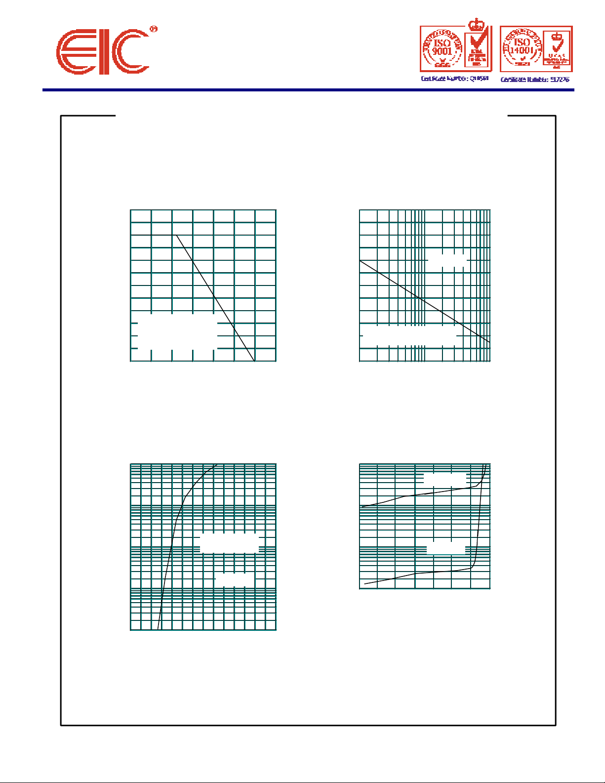
RATING AND CHARACTERISTIC CURVES ( BR3500 - BR3510 )
21147
42
400
0
0
28
102060
124640
HEAT-SINK MOUNTING, Tc
FIG.1 - DERATING CURVE FOR OUTPUT FIG.2 - MAXIMUM NON-REPETITIVE PEAK
RECTIFIED CURRENT FORWARD SURGE CURRENT
600
35
500
TJ = 50 °C
300
AMPERES
7.5" x 3.5" x 4.6" THK.
(19cm x 9cm x 11.8cm)
Al.-Finned plate
AMPERES
200
8.3 ms SINGLE HALF SINE WAVE
100
PEAK FORWARD SURGE CURRENT,
JEDEC METHOD
AVERAGE FORWARD OUTPUT CURRENT
0 25 50 75 100 125 150 175
CASE TEMPERATURE, ( °C)
NUMBER OF CYCLES AT 60Hz
FIG.3 - TYPICAL FORWARD CHARACTERISTICS FIG.4 - TYPICAL REVERSE CHARACTERISTICS
PER DIODE PER DIODE
100 10
TJ = 100 °C
10
1.0
100
Pulse Width = 300 µs
1.0
0.1
1 % Duty Cycle
FORWARD CURRENT, AMPERES
0.01
0.4 0.6 0.8 1.0 1.6
1.2 1.4
FORWARD VOLTAGE, VOLTS
TJ = 25 °C
0.1
0.01
REVERSE CURRENT, MICROAMPERES
TJ = 25 °C
80
100 1400 20 40 60 120
PERCENT OF RATED REVERSE
VOLTAGE, (%)
1.8
 Loading...