DYNEX MAS110S12, MAS110S10, MAS110S08, MAS110S06, MAS110S14 Datasheet

MAS110S
1/9
APPLICATIONS
● High Frequency High Power Choppers And Inverters.
● Ultrasonic Generators.
● Welding.
● PWM Inverters.
DESCRIPTION
The MAS 110S is a fast thyristor/diode module in an
electrically isolated package. The semiconductors are are
pressure contact mounted giving high resistance to
thermal fatigue, and having excellent heat dissipation
qualities.
Isolation medium is non-toxic alumina.
The MAS110S is recognised under the 'Recognised
Component Program of Underwriters Laboratories Inc.
USA. File number E151069.
VOLTAGE RATINGS
KEY PARAMETERS
V
DRM
1400V
I
TSM
2000A
I
T(AV)
per arm 110A
V
isol
2500V
t
q
10/12/15µs
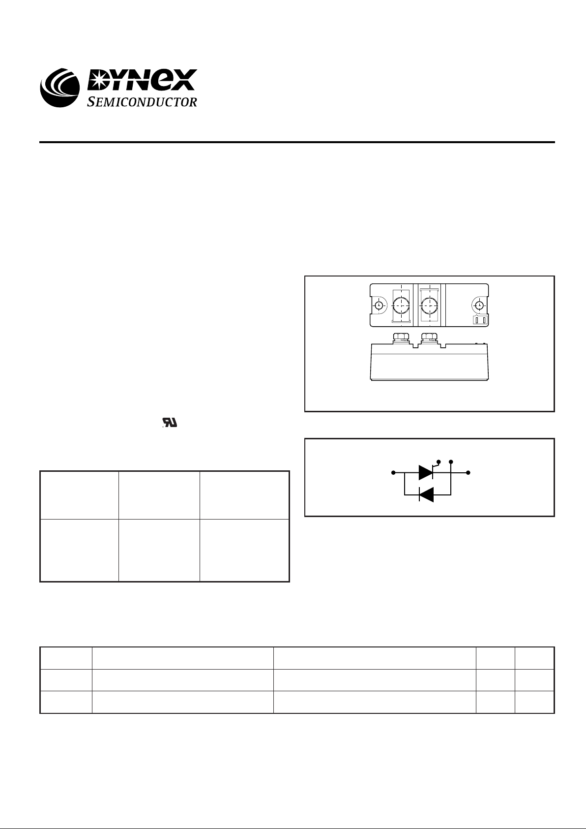
Fig.2 Single circuit
Conditions
Tvj = 125˚C,
I
DRM
= 50mA,
V
DSM
= V
DRM
+ 100V
For full description of part number see 'Ordering Information'.
Type Number
MAS110S 14
MAS110S 12
MAS110S 10
MAS110S 08
MAS110S 06
Repetitive Peak
Off-state Voltage
V
DRM
V
1400
1200
1000
800
600
Outline type code: MAS110S
See Package Details for further information.
THYRISTOR CURRENT RATINGS
Symbol Parameter Conditions UnitsMax.
I
T(AV)
Mean forward current
I
T(RMS)
RMS value
Half wave resistive load, T
case
= 75oC 110 A
T
case
= 75oC 175 A
G
1
K
1
1
2
Fig.1 Package outline (not to scale)
MAS110S
Fast Turn-off Asymmetric Thyristor/Diode Module
Replaces April 1999 version, DS4200-4.0 DS4200-5.0 January 2000

MAS110S
2/9
THYRISTOR SURGE RATINGS
Conditions
10ms half sine; T
case
= 125oC
V
R
= 0% V
DRM
Max. UnitsSymbol Parameter
I
TSM
Surge (non-repetitive) on-state current
I
2
tI
2
t for fusing 20.0 x 10³A2s
2.0 kA
THYRISTOR DYNAMIC CHARACTERISTICS
V
TM
ParameterSymbol Conditions
Maximum on-state voltage At 600A peak, T
case
= 25oC
I
DRM
Peak off-state current At V
DRM
, T
case
= 125oC
dV/dt Maximum linear rate of rise of off-state voltage To 60% V
DRM Tj
= 125oC, Gate open circuit
Min. Max. Units
- 2.9 V
-70mA
- 1000 V/µs
Repetitive 50Hz
- 500 A/µs
Rate of rise of on-state currentdI/dt
From 67% V
DRM
to 600A,
Gate source 20V, 20Ω
t
r
= < 0.5µs, Tj = 125˚C
V
T(TO)
Threshold voltage At Tvj = 125oC
r
T
On-state slope resistance At Tvj = 125oC
1.6-V
- 1.4 mΩ
Turn-off timet
q
µs10-
µs12-
µs15-
IT = 100A, Tj = 125˚C,
dIR/dt = 30A/µs, VGK = 0V
dV/dt = 20V/µs to 60%
V
DRM
, VR = 1V.
t
q
code: W
t
q
code: S
t
q
code: X

MAS110S
3/9
DIODE CURRENT RATINGS
Symbol Parameter Conditions UnitsMax.
I
T(AV)
Mean forward current
I
T(RMS)
RMS value
Half wave resistive load, T
case
= 75oC 112 A
T
case
= 75oC 175 A
DIODE SURGE RATINGS - PER ARM
Conditions
10ms half sine; T
case
= 130oC
V
R
= 0% V
RRM
Max. Units
Symbol
Parameter
I
FSM
Surge (non-repetitive) forward current
I
2
tI
2
t for fusing 61.25 x 10³A2s
3.5 kA
Conditions
At 600A, T
case
= 25˚C.
Max. Units
Symbol
Parameter
V
FM
Forward voltage
I
RRM
Peak reverse current 70 mA
2.65 V
At V
RRM
, T
case
= 125˚C.
t
rr
Reverse recovery time 1.3 µs
T
case
= 125˚C, dIR/dt = -50V/µs, IFM = 200A
V
TO
Threshold voltage 1.6 VAt Tvj = 125˚C.
Forward slope resistance 1.5 mΩAt Tvj = 125˚C.r
T
DIODE DYNAMIC CHARACTERISTICS
THYRISTOR GATE TRIGGER CHARACTERISTICS AND RATINGS
V
DRM
= 12V, T
case
= 25oC
ConditionsParameterSymbol
V
GT
Gate trigger voltage V
DRM
= 12V, T
case
= 25oC, RL = 30Ω
I
GT
Gate trigger current
V
RGM
Peak reverse gate voltage
I
FGM
Peak forward gate current Anode positive with respect to cathode
P
GM
Peak gate power -
P
G(AV)
Mean gate power
- 4.0 V
- 250 mA
- 7.0 V
-10A
-50W
-15W
Typ. Max. Units
Average timing = 10ms
 Loading...