

DIODES SBL3030PT, SBL3035PT, SBL3040PT, SBL3045PT, SBL3050PT Datasheet
...
Features
Schottky Barrier Chip
·
Guard Ring Die Construction for
·
Transient Protection
Low Power Loss, High Efficiency
·
High Surge Capability
·
High Current Capability and Low Forward
·
Voltage Drop
For Use in Low Voltage, High Frequency
·
Inverters, Free Wheeling, and Polarity
Protection Application
Plastic Material : UL Flammability
·
Classification Rating 94V-0
Mechanical Data
Case: Molded Plastic
·
Terminals: Plated Leads Solderable per
·
MIL-STD-202, Method 208
· Polarity: As Marked on Body
· Marking: Type Number
· Weight: 2.24 grams (approx.)
· Mounting Position: Any
SBL3030PT - SBL3060PT
30A SCHOTTKY BARRIER RECTIFIER
TO-3P
Dim Min Max
3.20 3.50
A
S
R
P*
*2 Places
N
A
H
J
K
L
Q
G
M
M
B
C
D
E
All Dimensions in mm
4.59 5.16
B
20.80 21.30
C
19.70 20.20
D
2.10 2.40
E
0.51 0.76
G
15.90 16.40
H
1.70 2.70
J
3.10Æ 3.30Æ
K
3.50 4.51
L
5.20 5.70
M
1.12 1.22
N
1.93 2.18
P
2.97 3.22
Q
11.70 12.80
R
S
4.30 Typical
Maximum Ratings and Electrical Characteristics
Single phase, half wave, 60Hz, resistive or inductive load.
For capacitive load, derate current by 20%.
O
FM
qJc
SBL
3030PT
R
j
Characteristic Symbol
Peak Repetitive Reverse Voltage
Working Peak Reverse Voltage
DC Blocking Voltage
RMS Reverse Voltage
Average Rectified Output Current @ TC= 95°C
Non-Repetitive Peak Forward Surge Current
8.3ms Single half sine-wave superimposed on rated load
(JEDEC Method)
Forward Voltage Drop @ IF= 15A, TC= 25°C
Peak Reverse Current @ TC= 25°C
at Rated DC Blocking Voltage @ T
Typical Junction Capacitance (Note 2)
Typical Thermal Resistance Junction to Case (Note 1)
Operating and Storage Temperature Range
Notes: 1. Thermal resistance junction to case mounted on heatsink.
2. Measured at 1.0MHz and applied reverse voltage of 4.0V DC.
(Note 1)
= 100°C
C
V
V
V
R(RMS)
I
V
I
R
T
j,TSTG
RRM
RWM
V
I
FSM
RM
C
@ TA= 25°C unless otherwise specified
SBL
3035PT
30 35 40 45 50 60 V
21 24.5 28 31.5 35 42 V
SBL
3040PT
0.55 0.70 V
-65 to +150 °C
SBL
3045PT
30 A
275 A
1.0
75
1100 pF
2.0 K/W
SBL
3050PT
SBL
3060PT
Unit
mA
DS23018 Rev. E-2 1 of 2 SBL3030PT - SBL3060PT
100
g
300
g
000
g
100
g
30
(AV)
g
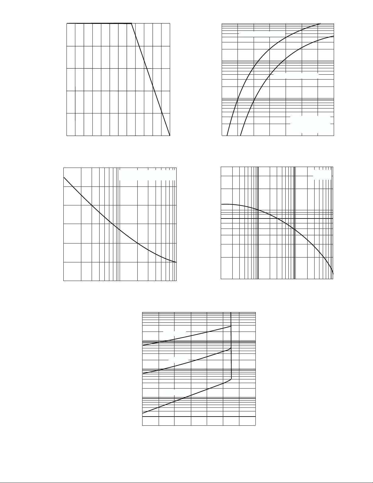
I , AVERAGE RECTIFIED CURRENT (A)
24
18
12
SBL3030PT - SBL30450PT
10
SBL3050PT - SBL3060PT
1.0
6
T = 25°C
j
Pulse width = 300 µs
F
0
0
50
T , CASE TEMPERATURE (°C)
C
Fi
. 1 Forward DeratingCurve
100
150
I , INSTANTANEOUS FORWARD CURRENT (A)
0.1
0.2 0.4 0.6 0.8
V , INSTANTANEOUS FORWARD VOLTAGE (V)
F
.2 Typical Fwd Characteristics per Element
Fi
2% duty cycle
FSM
I , PEAK FORWARD SURGE CURRENT (A)
8.3 ms single half-sine-wave
JEDEC method
250
200
150
100
50
0
1 10 100
NUMBER OF CYCLES AT 60 Hz
. 3 Max Non-Repetitive Peak Fwd Surge Current
Fi
10
T = 100°C
C
j
C , JUNCTION CAPACITANCE (pF)
4
1000
100
0.1 1.0 10 100
V , REVERSE VOLTAGE (V)
Fi
R
.4 Typical Junction Capacitance per Element
T = 25°C
j
f = 1MHz
T = 75°C
C
1.0
T = 25°C
C
R
I , INSTANTANEOUS REVERSE CURRENT (A)
0.1
0.01
04080
120
PERCENT OF PEAK REVERSE VOLTAGE (%)
.5 Typical Reverse Characteristics per Element
Fi
DS23018 Rev. E-2 2 of 2 SBL3030PT - SBL3060PT
 Loading...