

Page 1
e3
PDR3G
E
E1
b1
A
A2
A2
D
b2
b1
e
L1
L1
E
b1
D
b2
b1
e
D2
L
E2
L1
LEFT PIN
RIGHT PIN
Note: Pins Left & Right must
be electrically connected
at the printed circuit board.
BOTTOMSIDE
HEAT SINK
W
Features
· Glass Passivated Die Construction
· Low Leakage Current
· High Forward Surge Current Capability
· Lead Free Finish, RoHS Compliant (Note 1)
· "Green" Molding Compound (No Br, Sb)
· Qualified to AEC-Q101 Standards for High Reliability
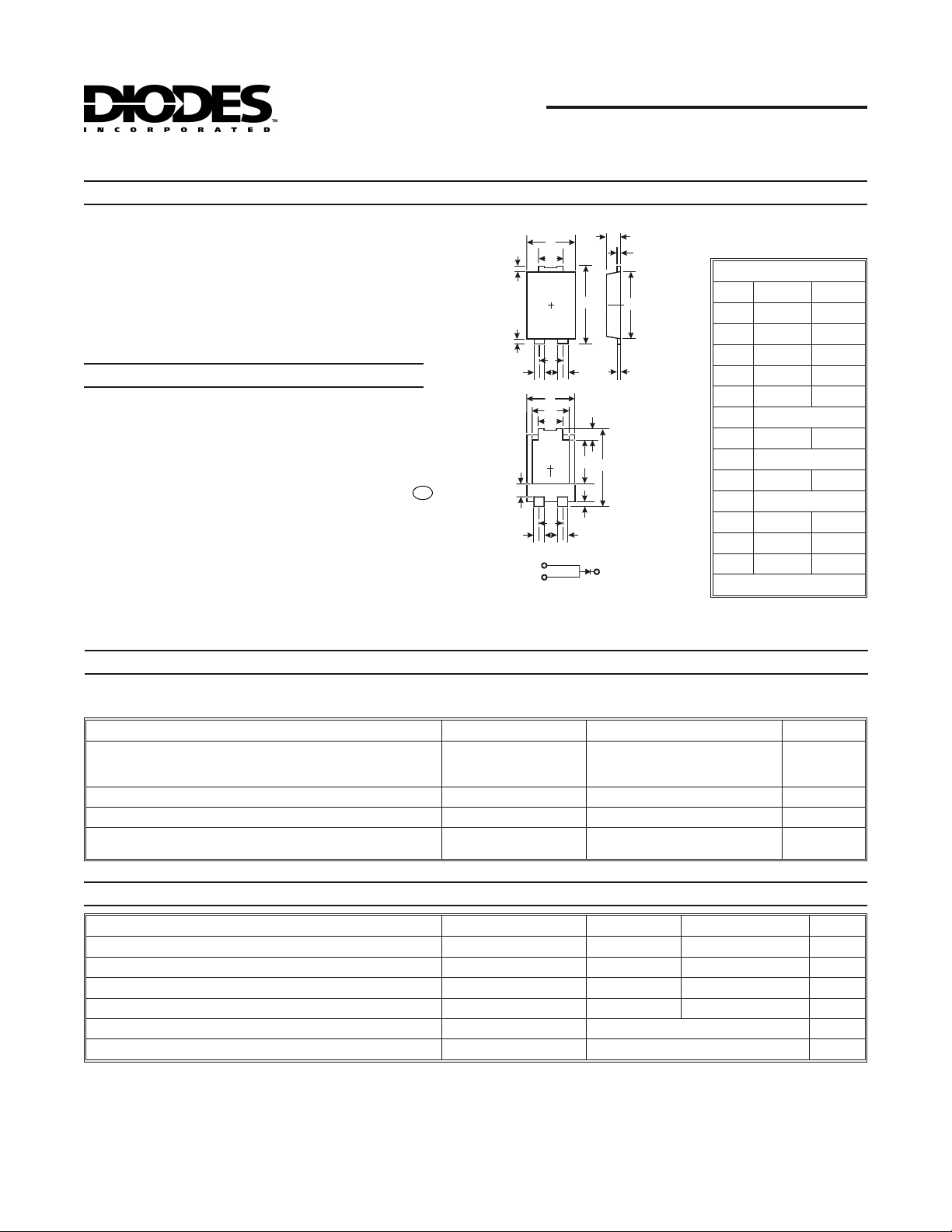
Mechanical Data
· Case: PowerDI
· Case Material: Molded Plastic, “Green” Molding
Compound. UL Flammability Classification Rating 94V-0
· Moisture Sensitivity: Level 1 per J-STD-020C
· Terminals: Finish – Matte Tin annealed over Copper
leadframe. Solderable per MIL-STD-202, Method 208
· Polarity: See Diagram
· Marking: See Page 3
· Weight: 0.095 grams (approximate)
ä
5
3A GLASS PASSIVATED RECTIFIER
PowerDI
ä
PowerDIä5
A
A2
b1
b2
D
D2
E
e
E1
E2
L
L1
W
Min Max
1.05 1.15
0.33 0.43
0.80 0.99
1.70 1.88
3.90 4.05
3.05 NOM
6.40 6.60
1.84 NOM
5.30 5.45
3.55 NOM
0.75 0.95
0.50 0.65
1.20 1.50
Dim
All Dimensions in mm
5
Maximum Ratings
@ TA = 25°C unless otherwise specified
Single phase, half wave, 60Hz, resistive or inductive load.
For capacitive load, derate current by 20%.
Characteristic Symbol
Peak Repetitive Reverse Voltage
Working Peak Reverse Voltage
DC Blocking Voltage
RMS Reverse Voltage
Average Rectified Output Current (See also figure 4)
Non-Repetitive Peak Forward Surge Current
8.3ms Single half sine-wave Superimposed on Rated Load
V
V
V
R(RMS)
I
RRM
RWM
V
R
I
O
FSM
Value
400 V
283 V
3 A
100 A
Thermal Characteristics
Characteristic Symbol Typ Max Unit
Thermal Resistance Junction to Soldering Point
Thermal Resistance Junction to Ambient Air (Note 2)
Thermal Resistance Junction to Ambient Air (Note 3)
Thermal Resistance Junction to Ambient Air (Note 4)
Operating Temperature Range
Storage Temperature Range
Notes: 1. RoHS revision 13.2.2003. Glass and High Temperature Solder Exemptions Applied, see EU Directive Annex Notes 5 and 7.
2. FR-4 PCB, 2 oz. Copper, minimum recommended pad layout per http://www.diodes.com/datasheets/ap02001.pdf. T
3. Polymide PCB, 2 oz. Copper, minimum recommended pad layout per http://www.diodes.com/datasheets/ap02001.pdf. T
4. Polymide PCB, 2 oz. Copper. Cathode pad dimensions 9.4mm x 7.2mm. Anode pad dimensions 2.7mm x 1.6mm. T
R
R
R
R
T
qJS
qJA
qJA
qJA
T
STG
¾ 2.0 °C/W
75 ¾ °C/W
65 ¾ °C/W
45 ¾ °C/W
j
-65 to +150 °C
-65 to +150 °C
= 25°C
A
= 25°C
A
= 25°C
A
Unit
DS30547 Rev. 7 - 2 1 of 3 PDR3G
PowerDI is a trademark of Diodes Incorporated. www.diodes.com ã Diodes Incorporated
Page 2
I , INSTANTANEOUS FORWARD CURRENT (A)
F
V , INSTANTANEOUS FORWARD VOLTAGE (V)
F
Fig. 1 Typical Forward Characteristics
10
1
100
0
0.2
0.4
0.6
0.8
1.0 1.2
100m
1m
10m
T = 25°C
j
T = 85°C
j
T = 150°C
j
T = -65°C
j
0
80
160
240
400
V , INSTANTANEOUS REVERSE VOLTAGE (V)
R
Fig. 2 Typical Reverse Characteristics
320
10n
1n
100n
I , INSTANTANEOUS REVERSE CURRENT (A)
R
T = +125°C
j
T = +150°C
j
T = +85°C
j
T = +25°C
j
T = -65°C
j
C , TOTAL CAPACITANCE (pF)
T
V , REVERSE VOLTAGE (V)
R
Fig. 3 Typical Total Capacitance vs. Reverse Voltage
0
10
20
30
40
0 5
10
15
20
25
30
f = 1 MHz
0
0.75
1.5
2.25
3.75
3.0
0
25
50
75
100
125
150
I , DC FORWARD CURRENT (A)
F
T , AMBIENT TEMPERATURE (°C)
A
Fig. 4 DC Forward Current Derating
Note 2
Note 4
Electrical Characteristics
@ TA = 25°C unless otherwise specified
Characteristic Symbol
Reverse Breakdown Voltage (Note 5)
Forward Voltage
Reverse Leakage Current (Note 5)
Reverse Recovery Time
Notes: 5. Short duration test pulse used to minimize self-heating effect.
V
(BR)R
V
F
I
R
t
rr
Min Typ Max Unit
400 ¾ ¾ V
¾ 0.92 1.15 V
¾¾0.015610
250
mA
¾ 3.0 ¾ ms
Test Condition
IR = 10mA
IF = 3A, TS = 25°C
TS = 25°C, VR = 400V
TS = 125°C, VR = 400V
IF = 0.5A, IR = 1.0A,
Irr = 0.25A
DS30547 Rev. 7 - 2 2 of 3 PDR3G
PowerDI is a trademark of Diodes Incorporated. www.diodes.com
Page 3

Ordering Information
R3G = Product type marking code
= Manufacturers’ code marking
YYWW = Date code marking
YY = Last two digits of year ex: 05 for 2005
WW = Week code 01 to 52
K = Factory Designator
YYWWK
R3G
0
1
2
3
4
0
1
3
2
4
5
P , FORWARD POWER DISSIPATION (W)
F
I , FORWARD CURRENT (A)
F
Fig. 5 Forward Power Dissipation
I
PK
I
AV
= 1 (DC)
0
30
150
180
120
90
60
0
100
200
300
400
T , DERATED AMBIENT TEMPERATURE (°C)
A
V , DC REVERSE VOLTAGE (V)
R
Fig. 6 Operating Temperature Derating
IMPORTANT NOTICE
Diodes Incorporated and its subsidiaries reserve the right to make modifications, enhancements, improvements, corrections or other changes without further
notice to any product herein. Diodes Incorporated does not assume any liability arising out of the application or use of any product described herein; neither
does it convey any license under its patent rights, nor the rights of others. The user of products in such applications shall assume all risks of such use and will
agree to hold Diodes Incorporated and all the companies whose products are represented on our website, harmless against all damages.
LIFE SUPPORT
Diodes Incorporated products are not authorized for use as critical components in life support devices or systems without the expressed written approval of the
President of Diodes Incorporated.
(Note 6)
Device
PDR3G-13
Notes: 6. For Packaging Details, go to our website at http://www.diodes.com/datasheets/ap02007.pdf.
Packaging Shipping
PowerDIä5 5000/Tape & Reel
Marking Information
DS30547 Rev. 7 - 2 3 of 3 PDR3G
PowerDI is a trademark of Diodes Incorporated. www.diodes.com
 Loading...