

Page 1
Please click here to visit our online spice models database.
Features
• Ultra-Small Surface Mount Package
• Guard Ring Die Construction for Transient Protection
• High Surge Capability
• Lead Free Finish, RoHS Compliant (Note 1)
• "Green" Molding Compound (No Br, Sb)
• Qualified to AEC-Q101 Standards for High Reliability
Maximum Ratings @T
= 25°C unless otherwise specified
A
Single phase, half wave, 60Hz, resistive or inductive load.
For capacitance load, derate current by 20%.
Characteristic Symbol Value Unit
Peak Repetitive Reverse Voltage
Working Peak Reverse Voltage
DC Blocking Voltage
RMS Reverse Voltage
Average Forward Current (See also figure 4)
Non-Repetitive Peak Forward Surge Current 8.3ms
Single Half Sine-Wave Superimposed on Rated Load
Top View
PD3S130H
1.0A SURFACE MOUNT SCHOTTKY BARRIER RECTIFIER
PowerDI
®
323
Mechanical Data
• Case: PowerDI®323
• Case Material: Molded Plastic, “Green” Molding Compound.
UL Flammability Classification Rating 94V-0
• Moisture Sensitivity: Level 1 per J-STD-020D
• Polarity: Cathode Band
• Terminals: Finish - Matte Tin annealed over Copper
leadframe. Solderable per MIL-STD-202, Method 208
• Marking Information: See Page 3
• Ordering Information: See Page 3
• Weight: 0.006 grams (approximate)
V
V
RRM
RWM
30 V
VR
V
R(RMS)
I
F(AV)
I
FSM
21 V
1.0 A
22 A
Thermal Characteristics
Characteristic Symbol Typ Max Unit
Thermal Resistance Junction to Soldering Point
Thermal Resistance Junction to Ambient Air (Note 2) @ T
Thermal Resistance Junction to Ambient Air (Note 3) @ T
Operating and Storage Temperature Range
Electrical Characteristics @T
Characteristic Symbol Min Typ Max Unit Test Condition
Reverse Breakdown Voltage (Note 4)
Forward Voltage
Leakage Current (Note 4)
Total Capacitance
Notes: 1. EU Directive 2002/95/EC (RoHS). All applicable RoHS exemptions applied, see EU Directive 2002/95/EC Annex Notes.
PowerDI is a registered trademark of Diodes Incorporated.
PD3S130H
Document number: DS30694 Rev. 7 - 2
2. FR-4 PCB, 2 oz. Copper, minimum recommended pad layout per http://www.diodes.com/datasheets/ap02001.pdf.
3. Polymide PCB, 2 oz. Copper, minimum recommended pad layout per http://www.diodes.com/datasheets/ap02001.pdf.
4. Short duration pulse test used to minimize self-heating effect.
= 25°C unless otherwise specified
A
= 25°C
A
= 25°C
A
V
(BR)R
VF
IR
CT ⎯
www.diodes.com
1 of 3
30
⎯
⎯
⎯
⎯
⎯
R
JS
θ
R
JA
θ
R
JA
θ
TJ, T
STG
⎯ ⎯
0.35
0.42
0.47
0.7
10
40
⎯
0.45
⎯
⎯
100
⎯
⎯
177
128
V
V
μA
pF
-65 to +150
IR = 100μA
IF = 0.1A
IF = 0.7A
IF = 1.0A
VR = 5V, TA = 25°C
VR = 30V, TA = 25°C
VR = 10V, f = 1.0MHz
6
⎯
⎯
© Diodes Incorporated
°C/W
°C/W
°C/W
°C
June 2008
Page 2
P
P
OWER
PATIO
N
NSTAN
T
N
O
US FOR
R
C
URREN
T
NSTAN
TANEO
US R
R
CUR
REN
T
C, TOT
CAPACITANC
F
R
G
FOR
R
CUR
R
T
T
R
T
T
T
PERAT
U
R
C
PD3S130H
1.2
10,000
(mA)
1.0
1,000
(W)
0.8
D
100
0.6
WA
DISSI
10
0.4
,
D
0.2
10,000
(uA)
1,000
SE
EVE
R
I, I
0.001
1.2
(A)
1.0
0
0.5 1.0 1.5 2.0 2.5
0
I , AVERAGE FORWARD CURRENT (A)
F(AV)
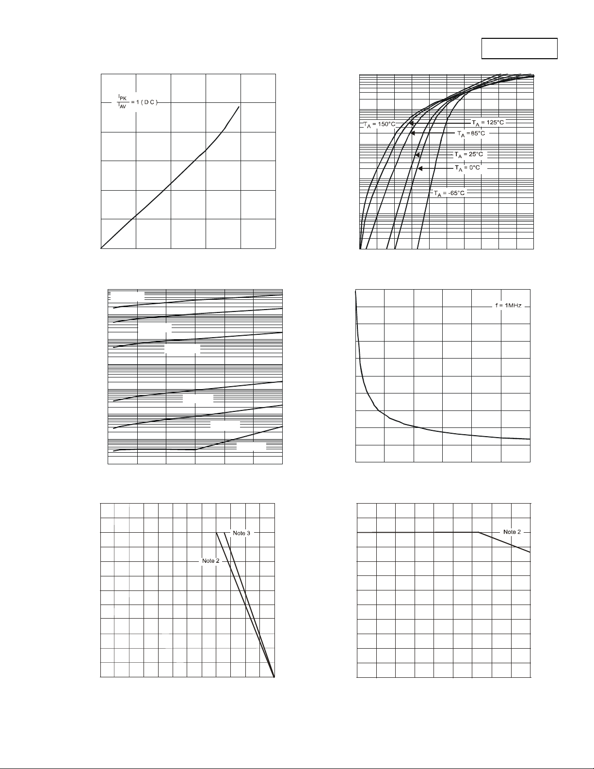
Fig. 1 Forward Power Dissipation
T = 150°C
A
T = 125°C
A
100
T = 85°C
A
10
1
T = 25°C
A
0.1
T = 0°C
A
0.01
10
0
5
V , INSTANTANEOUS REVERSE VOLTAGE (V)
R
15
20 25
Fig. 3 Typical Reverse Characteristics
T = -55°C
A
30
E
A
1
0.1
F
I, I
0
0.2
V , INSTANTANEOUS FORWARD VOLT AGE (V)
F
0.4
0.6 0.8
Fig. 2 Typical Forward Characteristics
1.0
200
180
)
160
140
E (p
120
100
80
AL
60
T
40
20
0
0
180
)
E (°
150
5
10 15
V , DC REVERSE VOLTAGE (V)
R
20
25 30
Fig. 4 Total Capacitance vs. Reverse Voltage
EN
0.8
120
D
EM
WA
E
A
0.6
0.4
90
60
ED AMBIEN
0.2
F(AV)
I, AVE
0
0255075
T , AMBIENT TEMPERATURE (°C)
A
100
Fig. 5 Forward Current Derating Curve
owerDI is a registered trademark of Diodes Incorporated.
P
PD3S130H
Document number: DS30694 Rev. 7 - 2
125
150
2 of 3
www.diodes.com
A
30
, DE
A
0
01020
V , DC REVERSE VOLTAGE (V)
R
Fig. 6 Oper at ing Temp er ature Derati ng
30
June 2008
© Diodes Incorporated
Page 3

PD3S130H
Ordering Information (Note 5)
Part Number Case Packaging
PD3S130H-7 PowerDI®323 3000/Tape & Reel
Notes: 5. For packaging details, go to our website at http://www.diodes.com/datasheets/ap02007.pdf.
Marking Information
Date Code Key
Year 2006 2007 2008 2009 2010 2011 2012
Code T U V W X Y Z
Month Jan Feb Mar Apr May Jun Jul Aug Sep Oct Nov Dec
Code 1 2 3 4 5 6 7 8 9 O N D
3(S)2
3S2 or 32 = Product Type Marking Code
YM = Date Code Marking
Y = Year (ex: T = 2006)
YM
M = Month (ex: 9 = September)
Package Outline Dimensions
C
B
D
L
E
L1
L4
L3
L1
A
H
L
E1
PowerDI®323
Dim Min Max Typ
A 2.40 2.60 2.50
B 1.85 1.95 1.90
C 1.20 1.30 1.25
D 0.60 0.70 0.65
E 0.78 0.98 0.88
E1 0.50 0.70 0.60
H 0.08 0.18 0.13
L 0.20 0.40 0.30
L1
⎯ ⎯
L3
⎯ ⎯
L4 0.40 0.80 0.60
All Dimensions in mm
1.40
0.20
Suggested Pad Layout
Diodes Incorporated and its subsidiaries reserve the right to make modifications, enhancements, improvements, corrections or other changes
without further notice to any product herein. Diodes Incorporated does not assume any liability arising out of the application or use of any product
described herein; neither does it convey any license under its patent rights, nor the rights of others. The user of products in such applications shall
assume all risks of such use and will agree to hold Diodes Incorporated and all the companies whose products are represented on our website,
harmless against all damages.
Diodes Incorporated products are not authorized for use as critical components in life support devices or systems without the expressed written
approval of the President of Diodes Incorporated.
Y2
X1 G
X2
Y1
IMPORTANT NOTICE
LIFE SUPPORT
Dimensions Value (in mm)
G 0.5
X1 2.0
X2 0.8
Y1 0.8
Y2 1.1
PowerDI is a registered trademark of Diodes Incorporated.
PD3S130H
Document number: DS30694 Rev. 7 - 2
3 of 3
www.diodes.com
June 2008
© Diodes Incorporated
 Loading...