

Page 1
A
f
Description
The PAM99700 is an open loop current mode control LED driver IC.
The PAM99700 can be programmed to operate in either a constant
frequency or constant off-time mode. It includes a 12 - 500V regulator
which allows it to work from a wide range of input voltages without the
need for an external low voltage supply. The PAM99700 includes a
PWM dimming input that can accept an external control signal with a
duty ratio of 0 - 100% and a frequency of up to a few kilohertz. It also
includes a 0 - 250mV linear dimming input which can be used for
linear dimming of the LED current.
The PAM99700 is ideally suited for buck LED drivers. Since the
PAM99700 operates in open loop current mode control, the controller
achieves good output current regulation without the need for any loop
compensation. PWM dimming response is limited only by the rate of
rise and fall of the inductor current, enabling very fast rise and fall
times. The PAM99700 requires only three external components (apart
from the power stage) to produce a controlled LED current making it
an ideal solution for low cost LED drivers.
Features
UNIVERSAL HIGH BRIGHTNESS LED DRIVER
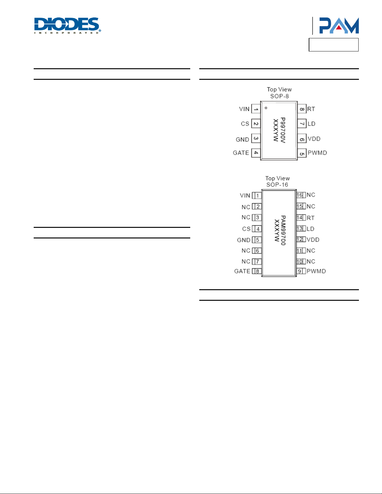
Pin Assignments
Product Line o
Diodes Incorporated
PAM99700
• Switch Mode Controller for Single Switch LED Drivers
• Open Loop Peak Current Controller
• Constant Frequency or Constant Off-Time Operation
• Linear and PWM Dimming Capability
• Requires Few External Components for Operation
• Application From a Few mA to More than 1A Output
PAM99700
Document number: DSxxxxx Rev. 1 - 1
www.diodes.com
Applications
• DC/DC or AC/DC LED Driver Applications
• RGB Backlighting LED Driver
• Back Lighting of Flat Panel Displays
• General Purpose Constant Current Source
• Signage and Decorative LED Lighting
1 of 12
October 2012
© Diodes Incorporated
Page 2
A
f
Typical Applications Circuit
Product Line o
Diodes Incorporated
PAM99700
Pin Descriptions
Pin
Name
VIN 1 1
CS 2 4
GND 3 5
GATE 4 8
PWMD 5 9
VDD 6 12
LD 7 13
RT 8 14
NC —
PAM99700
Document number: DSxxxxx Rev. 1 - 1
Pin Number
SOP-8 SOP-16
This pin is the input of a 12V-500V regulator.
This pin is the current sense pin used to sense the FET current by means of an external sense
resistor. When this pin exceeds the lower of either the internal 250mV or the voltage at the LD pin,
the gate output goes low.
Ground return for all internal circuitry. This pin must be electrically connected to the ground of the
power train.
This pin is the output gate driver for an external N-Channel power MOSFET.
This is the PWM dimming input of the IC. When this pin is pulled to GND, the gate driver is turned
off. When the pin is pulled high, the gate driver operates normally.
This is the power supply pin for all internal circuits. It must be bypassed with a low ESR capacitor
to GND (~ 10μF).
This pin is the linear dimming input an d sets the current sense threshold as long as the voltage at
the pin is less than 250mV (typ).
This pin sets the oscillator frequency. When a resistor is connected between RT and GND, the
PAM99700 operates in constant frequency mode. When the resistor is connected between RT
and GATE, the IC operates in constant off-time mode.
2, 3, 6, 7,
10, 11, 15, 16
Not connected.
2 of 12
www.diodes.com
Function
October 2012
© Diodes Incorporated
Page 3
A
f
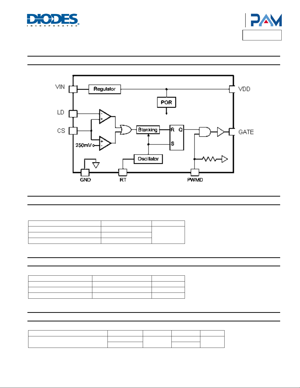
Functional Block Diagram
Product Line o
Diodes Incorporated
PAM99700
Absolute Maximum Ratings (@T
These are stress ratings only and functional operation is not implied. Exposure to absolute maximum ratings for prolonged time periods may
affect device reliability. All voltages are with respect to ground.
Parameter Rating Unit
Maximum Junction Temperature 150
Storage Temperature -65 to +150
Soldering Temperature 300, 5sec
Recommended Operating Conditions (@T
Parameter Rating Unit
Supply Voltage 12 to 500 V
Ambient Temperature Range -40 to +85 °C
Junction Temperature Range -40 to +125 °C
= +25°C, unless otherwise specified.)
A
°C
= +25°C, unless otherwise specified.)
A
Thermal Information
Parameter Package Symbol Max Unit
Thermal Resistance (Junction to Ambient)
PAM99700
Document number: DSxxxxx Rev. 1 - 1
SOP-8
SOP-16 110
www.diodes.com
θ
JA
3 of 12
115
°C/W
October 2012
© Diodes Incorporated
Page 4
A
f
Product Line o
Diodes Incorporated
PAM99700
Electrical Characteristics (@T
Parameter Symbol Test Conditions Min Typ Max Units
Input Voltage Range
Shutdown Mode Supply Current
Internally Regulated Voltage
Current Sense Pul-In Threshold Voltage
Current Sense Blanking Interval
Gate Sourcing Current
Gate Sinking Current
Gate Output Rise Time
Gate Output Fall Time
Oscillator Frequency
EN Threshold High
EN Threshold Low
Over Temperature Protection OTP 160 °C
OTP Hysteresis OTH 50 °C
PAM99700
Document number: DSxxxxx Rev. 1 - 1
= +25°C, unless otherwise specified.)
A
V
INDC
I
INSD
V
DD
V
CS,TH
T
BLANK
I
SOURCE
I
SINK
t
RISE
t
TALL
f
OSC
V
EH
V
EL
DC Input Voltage
Pin PWMD to GND
VIN > 20V
250 mV
250 Ns
V
V
C
C
= 0V
GATE
= VDD
GATE
= 1nF
GATE
= 1nF
GATE
= 510kΩ
R
T
RT = 226kΩ
VIN = 12V to 500V
VIN = 12V to 500V
4 of 12
www.diodes.com
12 500 V
0.1 mA
6 10 V
0.2 A
0.2 A
30 50 ns
30 50 ns
37 41 49
74 92 110
kHz
2.4 V
1.0 V
October 2012
© Diodes Incorporated
Page 5

A
f
Typical Performance Characteristics
(@TA = +25°C, VIN = 60V, 1WLED, RT = 510KΩ, L = 5.2mH, unless otherwise specified.)
Product Line o
Diodes Incorporated
PAM99700
PAM99700
Document number: DSxxxxx Rev. 1 - 1
5 of 12
www.diodes.com
October 2012
© Diodes Incorporated
Page 6

A
f
Product Line o
Diodes Incorporated
Typical Performance Characteristics (cont.)
(@TA = +25°C, VIN = 110VAC, 1WLED, RT = 510KΩ, L = 5.2mH, RCS = 0.68Ω, unless otherwise specified.)
PAM99700
PAM99700
Document number: DSxxxxx Rev. 1 - 1
www.diodes.com
6 of 12
October 2012
© Diodes Incorporated
Page 7

A
f
Product Line o
Diodes Incorporated
PAM99700
Application Information
The PAM99700 is optimized to drive buck LED drivers using open-loop peak current mode control. This method of control enables fairly accurate
LED current control without the need for high side current sensing or the design of any closed loop controllers. The IC uses very few external
components and enables both Linear and PWM dimming of the LED current.
A resistor connected to the RT pin programs the frequency of operation (or the off-time). The oscillator produces pulses at regular intervals.
These pulses set the SR fl ip- flop in the PAM99700 which causes the gate driver to turn on. The same pulses also start the blanking timer which
inhibits the reset input of the SR flip flop and prevent false turn-offs due to the turn-on spike. When the FET turns on, the current through the
inductor starts ramping up. This current flows through the external sense resistor R
comparators are constantly comparing the CS pin voltage to both the voltage at the LD pin and the internal 250mV. Once the blanking timer is
complete, the output of these comparators is allowed to reset the flip flop. When the output of either one of the two comparators goes high, the
flip flop is reset and the gate output goes low. The gate goes low until the SR flip flop is set by the oscillator. Assuming a 30% ripple in the
inductor, the current sense resistor R
Rcs = 0.25V (or V
Constant frequency peak current mode controlhas an inherent disadvantage - at duty cycles greater than 0.5, the control scheme goes into
subharmonic oscillations. To prevent this, an artificial slope is typically added to the current sense waveform. This slope compensation scheme
will affect the accuracy of the LED current in the present form. However, a constant off-time peak current control scheme does not have this
problem and can easily operate at duty cycles greater then 0.5 and also gives inherent input volt-age rejection making the LED current almost
insensitive to input voltage variations. But, it leads to variable frequency operation and the frequency range depends greatly on the input and
output voltage variation. PAM99700 makes it easy to switch between the two modes of operation by changing one connection (see oscillator
section).
)/1.15 * I
LD
can be set using:
CS
(A)
LED
Input Voltage Regulator
The PAM99700 can be powered directly from its VIN pin and can work from 12 - 500V DC at its VIN pin. When a voltage is applied at the VIN
pin, the PAM99700 maintains a constant 12V at the V
control the IC. The V
output gate driver.
ThePAM99700 can al so be operated by supplying a voltage at the V
internal linear regulator of the IC and the PAM99700 will operate directly off the voltage supplied at the V
voltage at the V
Although the VIN pin of the PAM99700 is rated up to 500V, the actual maximum voltage that can be applied is limited by the power dissipation in
the IC. For example, if an 8-pin (junction to ambient thermal resistance R
and has a maximum allowable temperature rise of the junction temperature limited to about ΔT = 100°C, the maximum voltage at the VIN pin
would be:
V
pin must be bypassed by a low ESR capacitor to provide a low impedance path for the high frequency current of the
DD
pin should not exceed 15V.
DD
1
T
Δ
=
)MAX(IN
=
•
R
I
INAJ
−θ
C100
°
°
1
•
mA2
W/C115
V435=
pin. This voltage is used to power the IC and any external resistor dividers needed to
DD
pin greater than the internally regulated voltage. This will turn off the
DD
= 115°C/W) PAM99700 draws about IIN = 2mA from the VIN pin,
θJ-A
and produces a ramp voltage at the CS pin. The
CS
pin. Please note that this external
DD
In these cases, to operate the PAM99700 from higher input voltages, a Zener diode can be added in series with the VIN pin to divert some of the
power loss from the PAM99700 to the Zener diode. In the above example, using a 100V zener diode will allow the circuit to easily work up to
500V.
The input current drawn from the VIN pin is a sum of the 1.0mA current drawn by the internal circuit and the current drawn by the gate driver
(which in turn depends on the switching frequency and the gate charge of the external FET).
+μ≈
*
In the above equation, f
the FET).
I
IN
A350
is the switching frequency and QG is the gate charge of the external FET (which can be obtained from the datasheet of
S
PAM99700
Document number: DSxxxxx Rev. 1 - 1
Q
f
s
G
7 of 12
www.diodes.com
October 2012
© Diodes Incorporated
Page 8

A
f
Product Line o
Diodes Incorporated
PAM99700
Application Information (cont.)
Current Sense
The current sense input of the PAM99700 goes to the non-inverting inputs of two comparators. The inverting terminal of one comparator is tied
to an internal 250mV reference whereas the inverting terminal of the other comparator is connected to the LD pin. The outputs of both these
comparators are fed into an OR gate and the output of the OR gate is fed into the reset pin of the flip-flop. Thus, the comparator which has the
lowest voltage at the inverting terminal determines when the GATE output is turned off.
The outputs of the comparators also include a 150-280ns blanking time which prevents spurious turn-offs of the external FET due to the turn-on
spike normally present in peak current mode control. In rare cases, this internal blanking might not be enough to filter out the turn-on spike. In
these cases, an external RC filter needs to be added between the external sense resistor
Please note that the comparators are fast (with a typical 80ns response time). Hence these comparators are more susceptible to be triggered by
noise than the comparators of the PAM99700. A proper layout minimizing external inductances will prevent false triggering of these comparators.
Oscillator
The oscillator in thePAM99700 is controlled by a single resistor connected at the RT pin. The equation governing the oscillator frequency is given
by:
F+Ω=
21380
)kHz(
5.5)k(RT
and the CS pin.
(RCS)
If the resistor is connected between RT and GND, PAM99700 operates in a constant frequency mode and the above equation determines the
time-period. If the resistor is connected between RT and GATE, the PAM99700 operates in a constant off-time mode and the below equation
determines the off-time.
+Ω
1.44)k(RT
=
T
OFF
(µS)
1.21
GATE Output
The gate output of the PAM99700 is used to drive and external FET. It is recommended that the gate charge of the external FET be less than
25nC for switching frequencies 100kHz and less than 15nC for switching frequencies >100kHz.
Linear Dimming
The Linear Dimming pin is used to control the LED current. There are two cases when it may be necessary to use the Linear Dimming pin. In
some cases, it may not be possible to find the exact R
cases, an external voltage divider from the V
desired voltage across R
Linear dimming may be desired to adjust the current level to reduce the intensity of the LEDs. In these cases, an external 0-250mV voltage can
be connected to the LD pin to adjust the LED current during operation.
To use the internal 250mV, the LD pin can be connected to V
Note: Although the LD pin can be pulled to GND, the output current will not go to zero. This is due to the presence of a minimum on-time (which
is equal to the sum of the blanking time and the delay to output time) which is about 450ns. This will cause the FET to be on for a minimum of
450ns and thus the LED current when LD = GND will not be zero. This current is also dependent on the input voltage, inductance value, forward
voltage of the LEDs and circuit parasitics. To get zero LED current, the PWMD pin has to be used.
CS
.
pin can be connected to the LD pin to obtain a voltage (less than 250mV) corresponding to the
DD
value required to obtain the LED current when the internal 250mV is used. In these
CS
.
DD
PWM Dimming
PWM Dimming can be achieved by driving the PWMD pin with a low frequency square wave signal. When the PWM signal is zero, the gate
driver is turned off and when the PWMD signal if high, the gate driver is enabled. Since the PWMD signal does not turn off the other parts of the
IC, the response of the PAM99700 to the PWMD signal is almost instantaneous. The rate of rise and fall of the LED current is thus determined
solely by the rise and fall times of the inductor current.To disable PWM dimming and enable the PAM99700 permanently, connect the PWMD pin
.
to V
DD
Thermal Protection
When the die temperature exceeds +160°C, a reset occurs and the reset remains until the temperature decrease to +110°C, at which time the
circuit can be restarted.When the die temperature exceeds +160°C, a reset occurs and the reset remains until the temperature decrease to
+110°C, at which time the circuit can be restarted.
PAM99700
Document number: DSxxxxx Rev. 1 - 1
8 of 12
www.diodes.com
October 2012
© Diodes Incorporated
Page 9

A
f
Ordering Information
Product Line o
Diodes Incorporated
PAM99700
Marking Information
Part Number Package Type Standard Package
PAM99700AC SOP-8L 2500 Units/Tape&Reel
PAM99100BD SOP-16L 2500 Units/Tape&Reel
PAM99700
Document number: DSxxxxx Rev. 1 - 1
9 of 12
www.diodes.com
October 2012
© Diodes Incorporated
Page 10

A
f
Package Outline Dimensions (All dimensions in mm.)
SOP-8
Product Line o
Diodes Incorporated
PAM99700
PAM99700
Document number: DSxxxxx Rev. 1 - 1
10 of 12
www.diodes.com
October 2012
© Diodes Incorporated
Page 11

A
f
Package Outline Dimensions (cont.) (All dimensions in mm.)
SOP-16
Product Line o
Diodes Incorporated
PAM99700
PAM99700
Document number: DSxxxxx Rev. 1 - 1
11 of 12
www.diodes.com
October 2012
© Diodes Incorporated
Page 12

A
f
Product Line o
Diodes Incorporated
PAM99700
DIODES INCORPORATED MAKES NO WARRANTY OF ANY KIND, EXPRESS OR IMPLIED, WITH REGARDS TO THIS DOCUMENT,
INCLUDING, BUT NOT LIMITED TO, THE IMPLIED WARRANTIES OF MERCHANTABILITY AND FITNESS FOR A PARTICULAR PURPOSE
(AND THEIR EQUIVALENTS UNDER THE LAWS OF ANY JURISDICTION).
Diodes Incorporated and its subsidiaries reserve the right to make modifications, enhancements, improvements, corrections or other changes
without further notice to this document and any product described herein. Diodes Incorporated does not assume any liability arising out of the
application or use of this document or any product described herein; neither does Diodes Incorporated convey any license under its patent or
trademark rights, nor the rights of others. Any Customer or user of this document or products described herein in such applications shall assume
all risks of such use and will agree to hold Diodes Incorporated and all the companies whose products are represented on Diodes Incorporated
website, harmless against all damages.
Diodes Incorporated does not warrant or accept any liability whatsoever in respect of any products purchased through unauthorized sales channel.
Should Customers purchase or use Diodes Incorporated products for any unintended or unauthorized application, Customers shall indemnify and
hold Diodes Incorporated and its representatives harmless against all claims, damages, expenses, and attorney fees arising out of, directly or
indirectly, any claim of personal injury or death associated with such unintended or unauthorized application.
Products described herein may be covered by one or more United States, international or foreign patents pending. Product names and markings
noted herein may also be covered by one or more United States, international or foreign trademarks.
This document is written in English but may be translated into multiple languages for reference. Only the English version of this document is the
final and determinative format released by Diodes Incorporated.
Diodes Incorporated products are specifically not authorized for use as critical components in life support devices or systems without the express
written approval of the Chief Executive Officer of Diodes Incorporated. As used herein:
A. Life support devices or systems are devices or systems which:
1. are intended to implant into the body, or
2. support or sustain life and whose failure to perform when properly used in accordance with instructions for use provided in the
labeling can be reasonably expected to result in significant injury to the user.
B. A critical component is any component in a life support device or system whose failure to perform can be reasonably expected to cause the
failure of the life support device or to affect its safety or effectiveness.
Customers represent that they have all necessary expertise in the safety and regulatory ramifications of their life support devices or systems, and
acknowledge and agree that they are solely responsible for all legal, regulatory and safety-related requirements concerning their products and any
use of Diodes Incorporated products in such safety-critical, life support devices or systems, notwithstanding any devices- or systems-related
information or support that may be provided by Diodes Incorporated. Further, Customers must fully indemnify Diodes Incorporated and its
representatives against any damages arising out of the use of Diodes Incorporated products in such safety-critical, life support devices or systems.
Copyright © 2012, Diodes Incorporated
www.diodes.com
IMPORTANT NOTICE
LIFE SUPPORT
PAM99700
Document number: DSxxxxx Rev. 1 - 1
12 of 12
www.diodes.com
October 2012
© Diodes Incorporated
 Loading...