

Page 1
A
f
Description
The PAM8902A is a mono, Class-D audio amplifier with integrated
boost convertor designed for piezo and ceramic speakers. The
PAM8902A is capable for driving a ceramic/piezo speaker with
(0.6Vrms) from a 3.6V power supply. The PAM8902A's boost
30V
PP
converter operates at a fixed frequency of 1.5MHz and provides a
17.5V supply with a minimum number of external components. The
three gain mode of 18dB, 22dB and 26dB is easy for using. PAM
unique ant i -saturat ion technology which detects output signal clip
due to the over level input signal suppress the output signal clip
automatically. PAM8902A features an integrated audio low pass filter
that rejects high frequency noise, thus improving audio fidelity.
PAM8902A also provides thermal, over current, under and over
voltage protection.
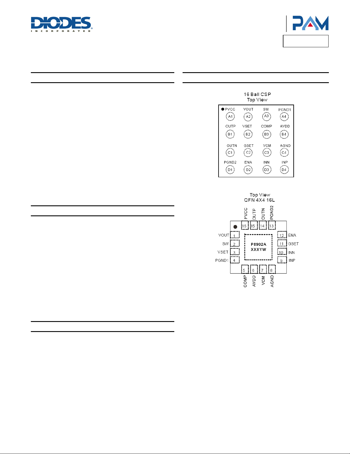
The PAM8902A is available in a 16-ball 1.95mm x 1.95mm CSP
package and 16-pin QFN4x4 package.
Product Line o
Diodes Incorporated
PAM8902A
30 VPP MONO CLASS-D AUDIO AMPLIFIER FOR
PIEZO/CERAMIC SPEAKERS WITH ANTI-SATURATION
Pin Assignments
Features
• Supply Voltage Range from 2.7V to 5.5V package.
• 30V
• Integrated Boost Converter Generates 17.5V Supply
• Programmable Soft-Start
• Unique Anti-Saturation Function
• Small Boost Converter Inductor
• Selectable Gain of 18dB, 22dB, and 26dB
• Selectable Boost output voltage of 8V, 12V, and 17.5V
• Low Shutdown Current: <1µA
• Build in Thermal, OCP, UVLO, OVP
• Available in Space Saving Packages:
Output Load Voltage from a 2.7V Supply
PP
(Refer to “Application Notes”)
16-ball 1.95mm x 1.95mm CSP package
16-pin QFN4x4 package
Applications
• Wireless or Cellular Handsets
• Portable DVD Player
• Personal Digital Assistants (PDAs )
• Electronic Dictionaries
• Digital Still Cameras
PAM8902A
Document number: DSxxxxx Rev. 1 - 3
1 of 12
www.diodes.com
February 2013
© Diodes Incorporated
Page 2
A
f
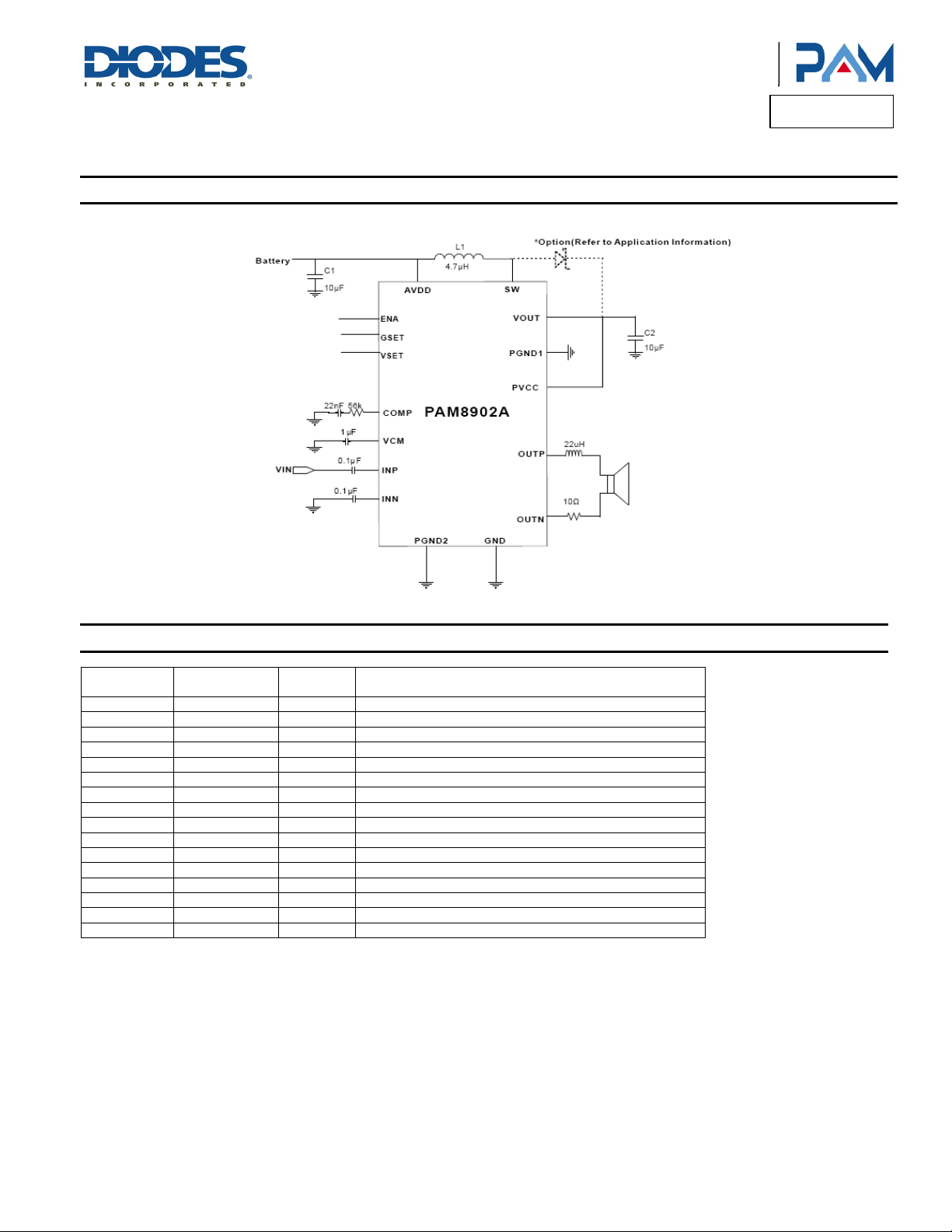
Typical Applications Circuit
Product Line o
Diodes Incorporated
PAM8902A
Pin Descriptions
Bump
(CSP)
A1 13 PVCC Audio Amplifier Power Supply
A2 1 VOUT Boost Convertor Output
A3 2 SW Boost Convertor Switching Node
A4 4 PGND1 Boost Convertor Power Ground
B1 15 OUTP Positive Differential Audio Output
B2 3 VSET Boost Convertor Output Voltage Setting(8V,12V,17.5V)
B3 5 COMP Boost Convertor Compensation
B4 6 AVDD Power Supply
C1 14 OUTN Negative Differential Audio Output
C2 11 GSET AmplifierGain Setting. (Refer to "Application Notes")
C3 7 VCM Common Mode Bypass Cap
C4 8 AGND Analog Ground
D1 13 PGND2 Class D PowerGround
D2 12 ENA Whole Chip Enable
D3 10 INN Negative Differential Audio Input
D4 9 INP Positive Differential Audio Input
Pin Number
(QFN)
Pin
Name
Function
PAM8902A
Document number: DSxxxxx Rev. 1 - 3
2 of 12
www.diodes.com
February 2013
© Diodes Incorporated
Page 3
A
f
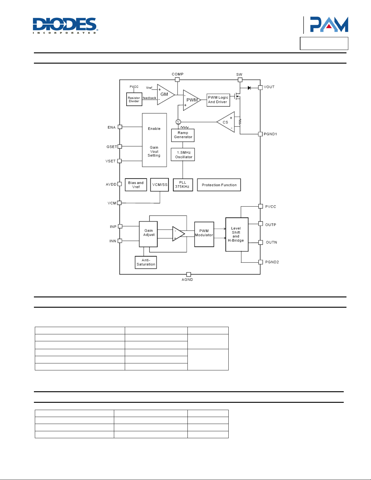
Functional Block Diagram
Product Line o
Diodes Incorporated
PAM8902A
Absolute Maximum Ratings (@T
These are stress ratings only and functional operation is not implied. Exposure to absolute maximum ratings for prolonged time periods may
affect device reliability. All voltages are with respect to ground.
Parameter Rating Unit
Supply Voltage 6.0
Input Voltage
Maximum Junction Temperature +150
Storage Temperature -65 to +150
Soldering Temperature 250, 10 sec
= +25°C, unless otherwise specified.)
A
-0.3 to V
DD
+0.3
V
°C
Recommended Operating Conditions (@T
= +25°C, unless otherwise specified.)
A
Parameter Rating Unit
Supply Voltage Range 2.7 to 5.5 V
Ambient Temperature Range -40 to +85 °C
Junction Temperature Range -40 to +125 °C
PAM8902A
Document number: DSxxxxx Rev. 1 - 3
3 of 12
www.diodes.com
February 2013
© Diodes Incorporated
Page 4
A
f
Product Line o
Diodes Incorporated
PAM8902A
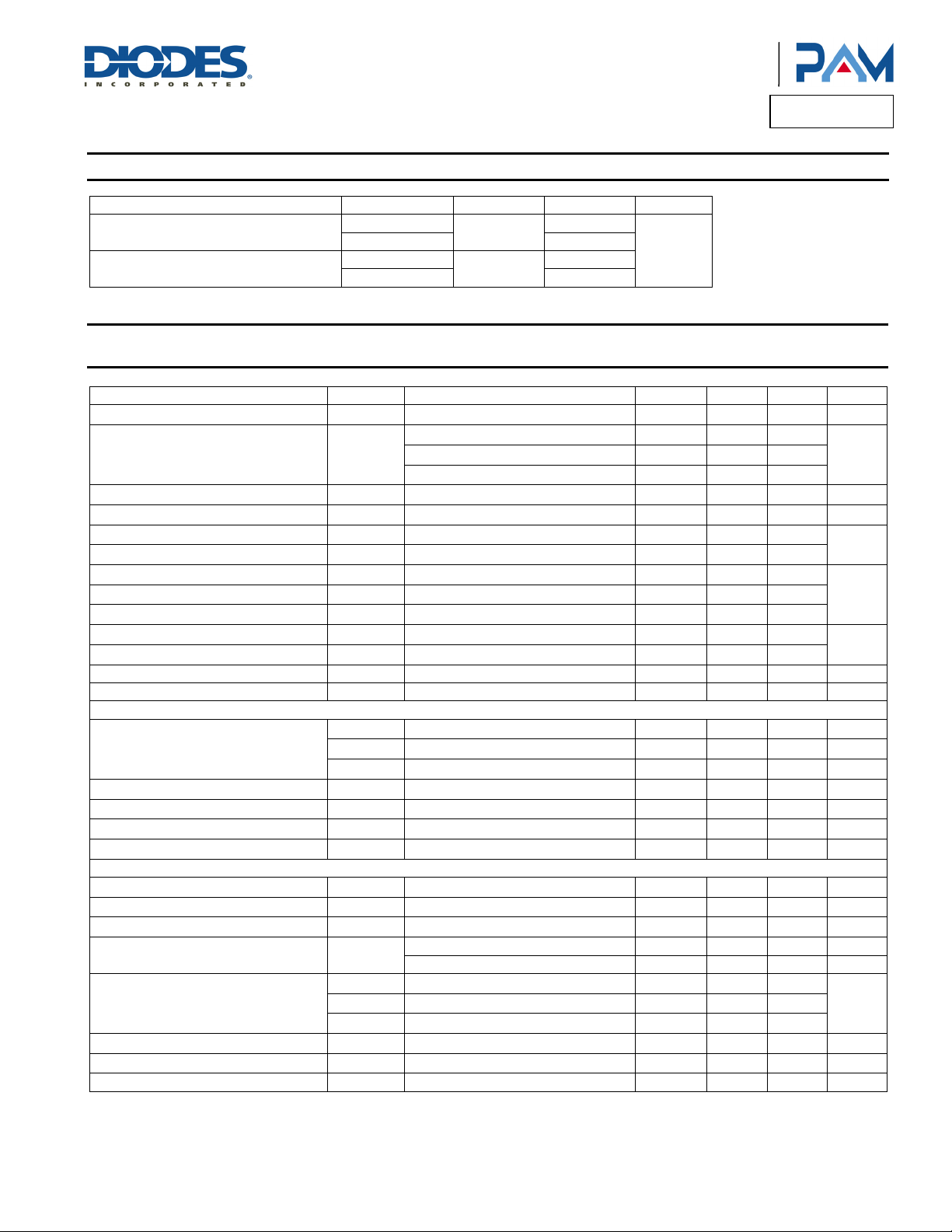
Thermal Information
Parameter Package Symbol Max Unit
Thermal Resistance (Junction to Ambient)
Thermal Resistance (Junction to Case)
CSP
QFN4x4-16 37
CSP
QFN4x4-16 2
JA
JC
90 – 220
75
°C/W
Electrical Characteristics
(@TA = +25°C, VDD = 3.6V, CL = 1µF, V
Parameter Symbol Test Conditions Min Typ Max Units
Input Voltage
Quiescent Current
Shutdown Current
Wake-Up Time
Chip Enable
Chip Disable
GSET/ VSET High
GSET/ VSET Floating
GSET/ VSET Low
Under Voltage Lockout Threshold UVLO
Under Voltage Lockout Hysteresis UVLO(H)
Thermal Shutdown Threshold OTP 150 °C
Thermal Shutdown Lockout Hysyeresis OTP(H) 30 °C
Boost Converter
Output Voltage
Current Limit
Lowside MOSFET R
RLS IO = 50mA
DS(ON)
Boost Switching Frequency
Over Voltage Protection Threshold
Class D
Class D Amplifier Switching Frequency
Common Mode Reject Ratio CMRR
Output Offset Voltage
R
RP
DS(ON)
Closed-Loop Voltage Gain
Power Supply Reject Ratio PSRR
Total Harmonic Distortion Plus Noise THD+N
Signal to Noise Ratio SNR Input AC Ground, A-Weighting 90 dB
PAM8902A
Document number: DSxxxxx Rev. 1 - 3
floating, R
SET
LOAD
V
DD
I
Q
I
SD
T
WU
V
EH
V
EL
V
H
V
F
V
L
V
1 V
O
VO2 V
VO3 V
C
L
f
OSCB
V
OVP
f
OSCD
V
OS
1 G
A
V
AV2 G
AV3 G
= 10, L
EN > 1.2V, V
EN > 1.2V, V
EN > 1.2V, V
= 22µh with external schottky diodes, unless otherwise specified.)
LOAD
2.7 5.5 V
= High
SET
= Floating
SET
= GND
SET
30 48
10 18
5 12
mA
EN = 0V 0.1 1 µA
EN from Low to High 40 mS
1.2
0.4
VDD -0.5
1
VDD
VDD -1
V
V
0 0.5
V
from High to Low
DD
V
from Low to High
DD
= Low, No Load
SET
= Floating, No Load
SET
= High, No Load
SET
2.2
0.2
V
7.2 8.0 8.8 V
10.8 12.0 13.2 V
16.0 17.5 19.0 V
Average Input Current 0.8 A
0.5
1.1 1.5 1.9 MHz
18 V
Input AC-GND 225 375 475 KHz
V
= ±100mV, VDD = 3.6V
IN
60 dB
Output Offset Voltage 5 50 mV
High Side 1.5
Low Side 0.6
= High, VO = 1V
SET
= Floating, VO = 1V
SET
= Low, VO = 1V
SET
200m V
V
O
Supply Ripple @ 217Hz
PP
= 5VRMS
4 of 12
www.diodes.com
RMS
RMS
RMS
25 26 27
21 22 23
dB
17 18 19
70 dB
0.3 %
February 2013
© Diodes Incorporated
Page 5
A
f
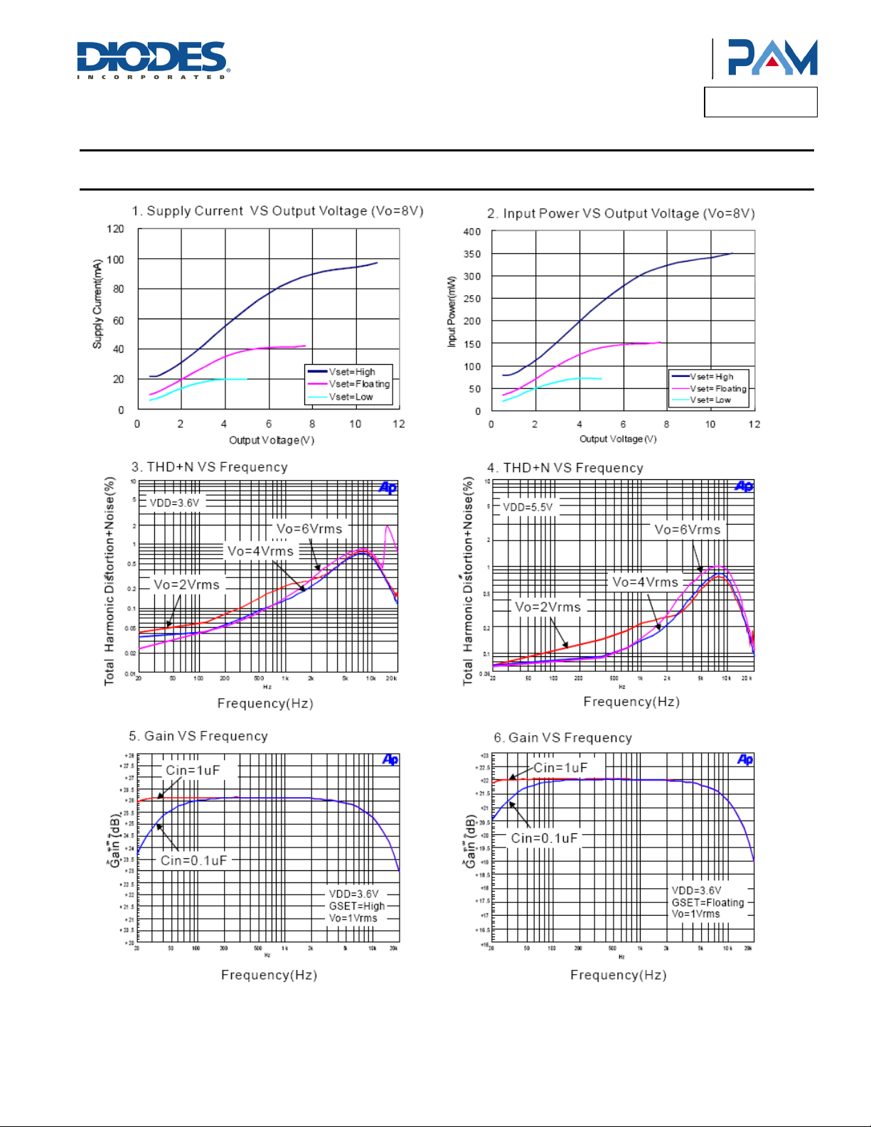
Typical Performance Characteristics (@T
L
= 22µH, with external schottky diode, unless otherwise specified.)
LOAD
Product Line o
Diodes Incorporated
= +25°C, VDD = 3.6V, CL = 1µF, L = 4.7µH, V
A
floating, R
SET
PAM8902A
= 10,
LOAD
PAM8902A
Document number: DSxxxxx Rev. 1 - 3
5 of 12
www.diodes.com
February 2013
© Diodes Incorporated
Page 6
A
f
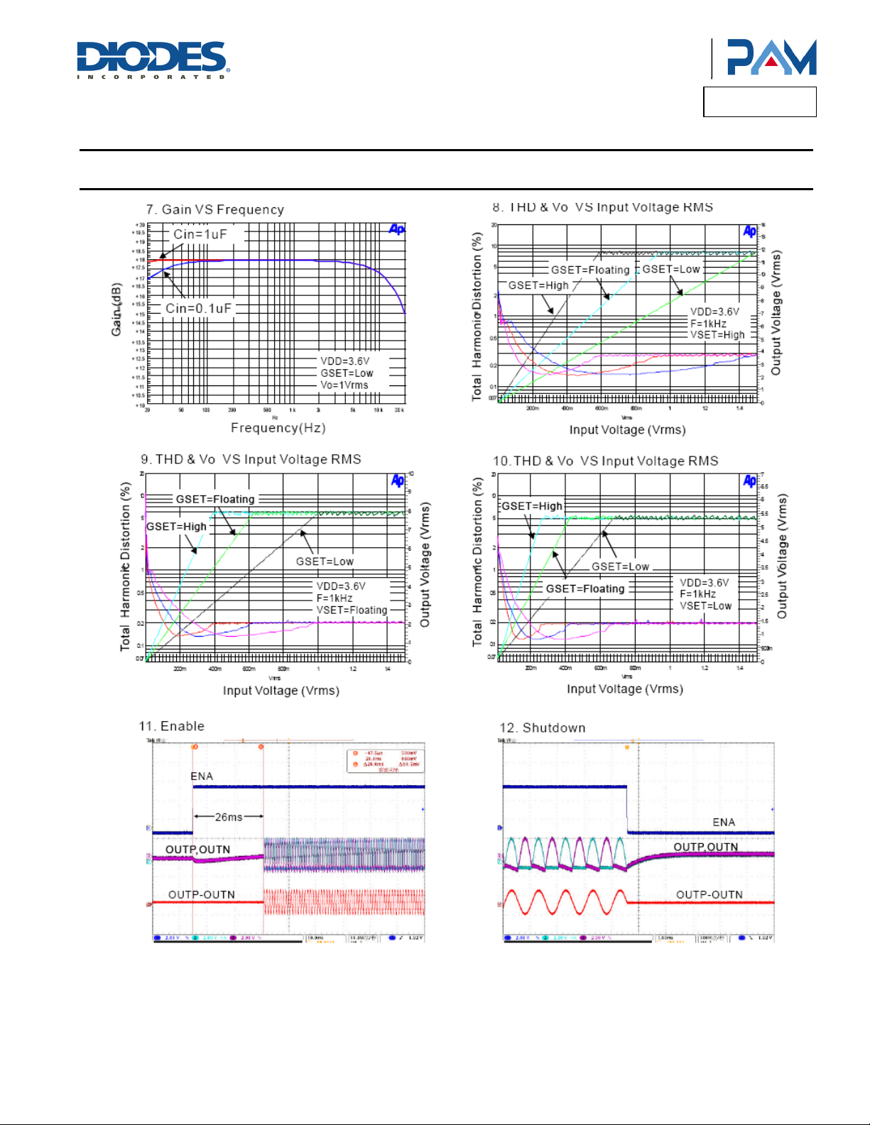
Typical Performance Characteristics (cont.) (@T
L
= 22µH, with external schottky diode, unless otherwise specified.)
LOAD
Product Line o
Diodes Incorporated
= +25°C, VDD = 3.6V, CL = 1µF, L = 4.7µH, V
A
floating, R
SET
PAM8902A
=10,
LOAD
PAM8902A
Document number: DSxxxxx Rev. 1 - 3
6 of 12
www.diodes.com
February 2013
© Diodes Incorporated
Page 7
A
f
Product Line o
Diodes Incorporated
PAM8902A
Application Information
Select Boost Converter Output Voltage
The V
Gain Setting and Input Resistance (RI)
Gain setting function is only available in disable condition (ENA = low) and need to follow the sequence as pull ENA to low (disable the IC) first,
and change the GSET voltage between high, floating, low, then pull ENA to high (enable the IC).
The input resistors (R
Where R
in fully differential amplifiers. The balance of the output on the reference voltage depends on matched ratios of the resistors. CMRR, PSRR, and
cancellation of the second harmonic distortion diminish if resistor mismatch occurs. Therefore, it is recommended to use 1% tolerance resistors
or better to keep the performance optimized. Matching is more important than overall tolerance. Resistor arrays with 1% matching can be used
with a tolerance greater than 1%.
Place the input resistors very close to the PAM8902A to limit noise injection on the high-impedance nodes. For optimal performance the gain
should be set to lower. Lower gain allows the PAM8902A to operate at its best, and keeps a high voltage at the input making the inputs less
susceptible to noise. In addition to these features, higher value of R
Anti-Saturation/Clipping Function
The anti-saturation circuitry detects the duty cycle of the PWM output. When the output starts to exhibit clipping, the gain is automatically
decreased with an attack time of 100µs per step a release time of 186ms per step. The following table describes the operation:
Attenuation Range The gain control range when anti-saturation is active.
PAM8902A
Document number: DSxxxxx Rev. 1 - 3
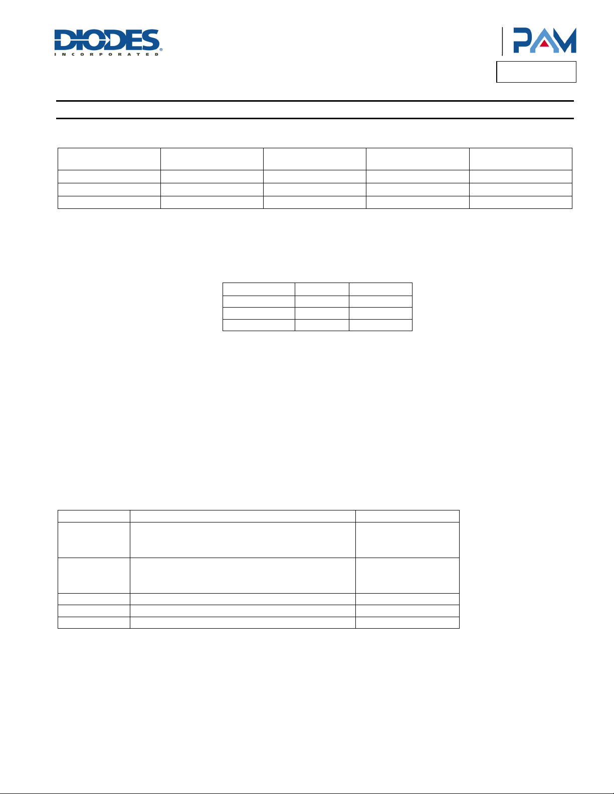
pin sets the boost converter output voltage to 8V, 12V or 17.5V. V
SET
Pin Configuration
V
SET
Min Max PVCC Voltage
High AVDD – 0.5 AVDD 17.5V
Floating 1V AVDD – 1V 12V
Low GND 0.5V 8V
= RIN + REX) set the gain of the amplifier according to Equation 1 when anti-saturation is inactive.
I
G = 20 Log [12.8*R
G
R
SET
pin configuration table as below:
SET
/ (RIN + REX)] (dB)
F
R
IN
FB
Audio Amplifier
Maximum Output Voltage
11 V
RMS
8 V
RMS
5 V
RMS
High 77.4k 122.6k
Floating 100k 100k
Low 122.6k 77.4k
is a 77.4K internal resistor, REX is the external input resistor, RF is a 122.6K internal resistor. Resistor matching is very important
IN
minimizes pop noise.
I
Variable Description Value
= High)
SET
= Floating)
SET
= Low)
SET
= High)
SET
= Floating)
SET
= Low)
SET
Gain
The original gain of the device when the Anti-saturation is
inactive.
26dB (G
22dB (G
18dB (G
-26dB (G
-22dB (G
-18dB (G
Step Size Gain adjust step size. 0.25dB/Step
Attack Time The minimum time between two gain decrements. 100µs
Release Time The minimum time between two gain increments. 186ms
7 of 12
www.diodes.com
(VPP = 31.1V)
(VPP = 22.6V)
(VPP = 14.1V)
February 2013
© Diodes Incorporated
Page 8

A
f
Product Line o
Diodes Incorporated
PAM8902A
Application Information (cont.)
Input Capacitors (CI)
In the typical application, an input capacitor, CI, is required to allow the amplifier to bias the input signal to the proper DC level for optimum
operation. In this case, C
equation:
It is important to consider the value of C
specification calls for a flat bass response are down to 150Hz.
Equation is reconfigured as followed:
When input resistance variation is considered, the C
capacitor is the leakage path from the input source through the input network (C
voltage at the input to the amplifier that reduces useful headroom, especially in high gain applications. For this reason, a low-leakage tantalum or
ceramic capacitor is the best choice. When polarized capacitors are used, the positive side of the capacitor should face the amplifier input in
most applications as the DC level is held at V
capacitor polarity in the application.
=
f
=
C
I
Π
Decoupling Capacitor
The PAM8902 is a high-performance CMOS audio amplifier that requires adequate power supply decoupling to ensure the output total harmonic
distortion (THD) as low as possible.
The optimum decoupling is achieved by using two different types of capacitors that target on different types of noise on the power supply leads.
For higher frequency transients, spikes, or digital hash on the line, a good low equivalent series-resistance (ESR) ceramic capacitor, typically
1µF is placed as close as possible to the device AVDD pin for the best operation. For filtering lower frequency noise signals, a large ceramic
capacitor of 10µF or greater placed near the AVDD supply trace is recommended.
External Schottky Diode
Use external schottky diode can get the best driving capability and efficiency.
Since internal power diode has limited driving capability, only in following conditions customer can remove the external schottky diode to reduce
the cost.
= Low or Floating and CL less than 1µF.
1. V
SET
2. The signal frequency less than 4KHz.
3. Haptic application (50–500Hz).
Shutdown Operation
In order to reduce power consumption while not in use, the PAM8902A contains shutdown circuitry amplifier off when a logic low is placed on the
ENA pin. By switching the ENA pin connected to GND, the PAM8902A supply current draw will be minimized in idle mode.
Under-Voltage Lock-Out (UVLO)
The PAM8902A incorporates circuitry designed to detect supply voltage. When the supply voltage drops to 2.2V or below, the PAM8902A goes
into a state of shutdown, and the device comes out of its shutdown state and restore to normal function only when reset the power supply or
ENA pin.
Over-Temperature Protection (OTP)
Thermal protection on the PAM8902A prevents the device from damage when the internal die temperature exceeds +150°C. There is a 15°C
tolerance on this trip point from device to device. Once the die temperature exceeds the set point, the device will enter the shutdown state and
the outputs are disabled, in this condition both OUTP and OUTN will become high impedance. This is not a latched fault. The thermal fault is
cleared once the temperature of the die decreased by 30°C. This large hysteresis will prevent motor boating sound well and the device begins
normal operation at this point with no external system interaction.
and the minimum input impedance RI form is a high-pass filter with the corner frequency determined in the follow
I
1
C
R2
ICΠ
I
as it directly affects the low frequency performance of the circuit. For example, when RI is 150k and the
I
1
R2
IFC
is 7nF, so one would likely choose a value of 10nF. A further consideration for this
I
, RI + RF) to the load. This leakage current creates a DC offset
I
/2, which is likely higher than the source DC level. Please note that it is important to confirm the
DD
PAM8902A
Document number: DSxxxxx Rev. 1 - 3
8 of 12
www.diodes.com
February 2013
© Diodes Incorporated
Page 9
A
f
Ordering Information
Product Line o
Diodes Incorporated
PAM8902A
Part Number Part Marking Package Type Standard Package
PAM8902AZER
PAM8902AKER
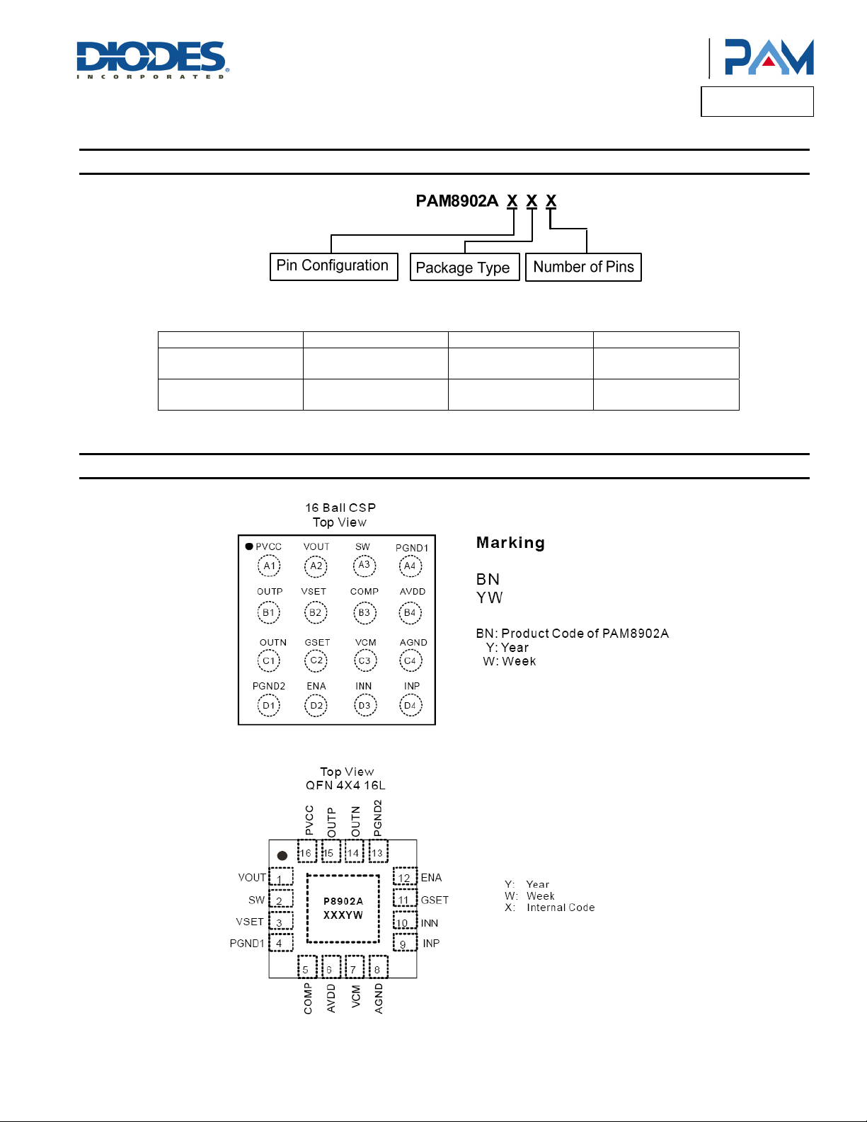
Marking Information
BN
YW
P8902A
XXXYW
CSP-16L 3000Units/Tape&Reel
QFN4x4-16L 3000Units/Tape&Reel
PAM8902A
Document number: DSxxxxx Rev. 1 - 3
9 of 12
www.diodes.com
February 2013
© Diodes Incorporated
Page 10
A
f
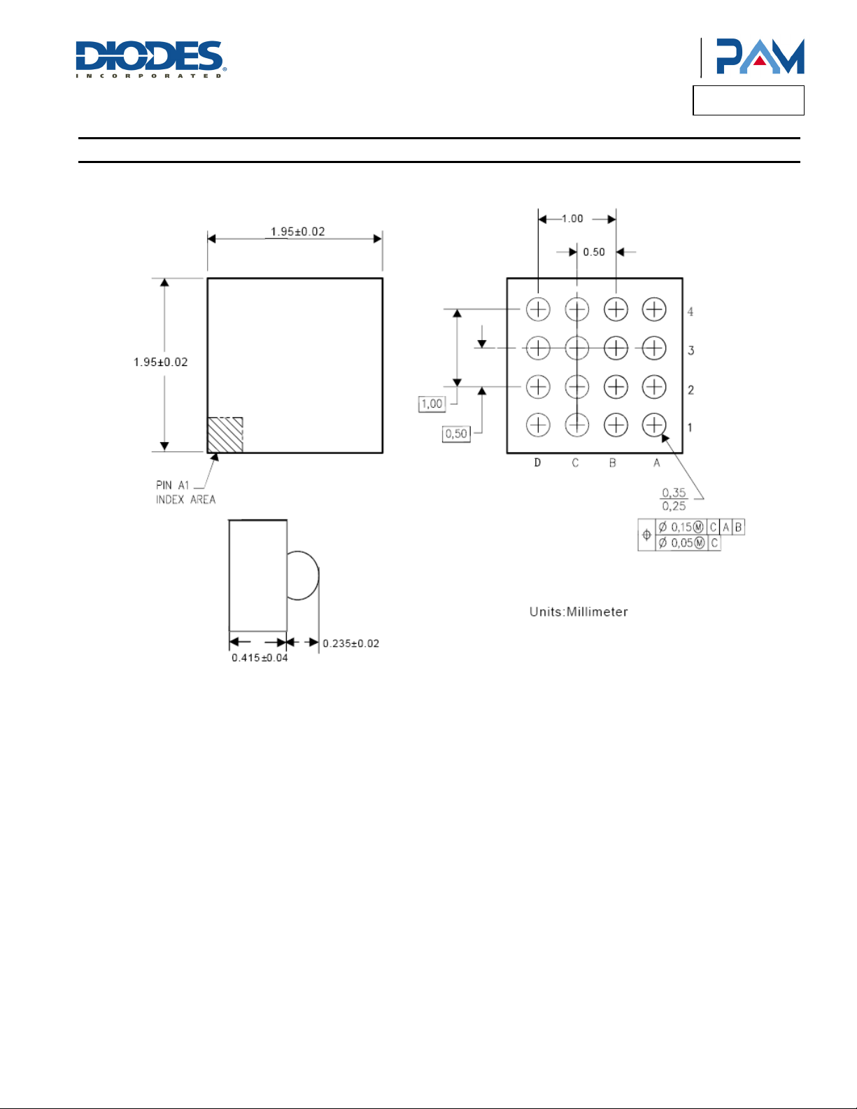
Package Outline Dimensions (All dimensions in mm.)
CSP-16
Product Line o
Diodes Incorporated
PAM8902A
PAM8902A
Document number: DSxxxxx Rev. 1 - 3
10 of 12
www.diodes.com
February 2013
© Diodes Incorporated
Page 11
A
f
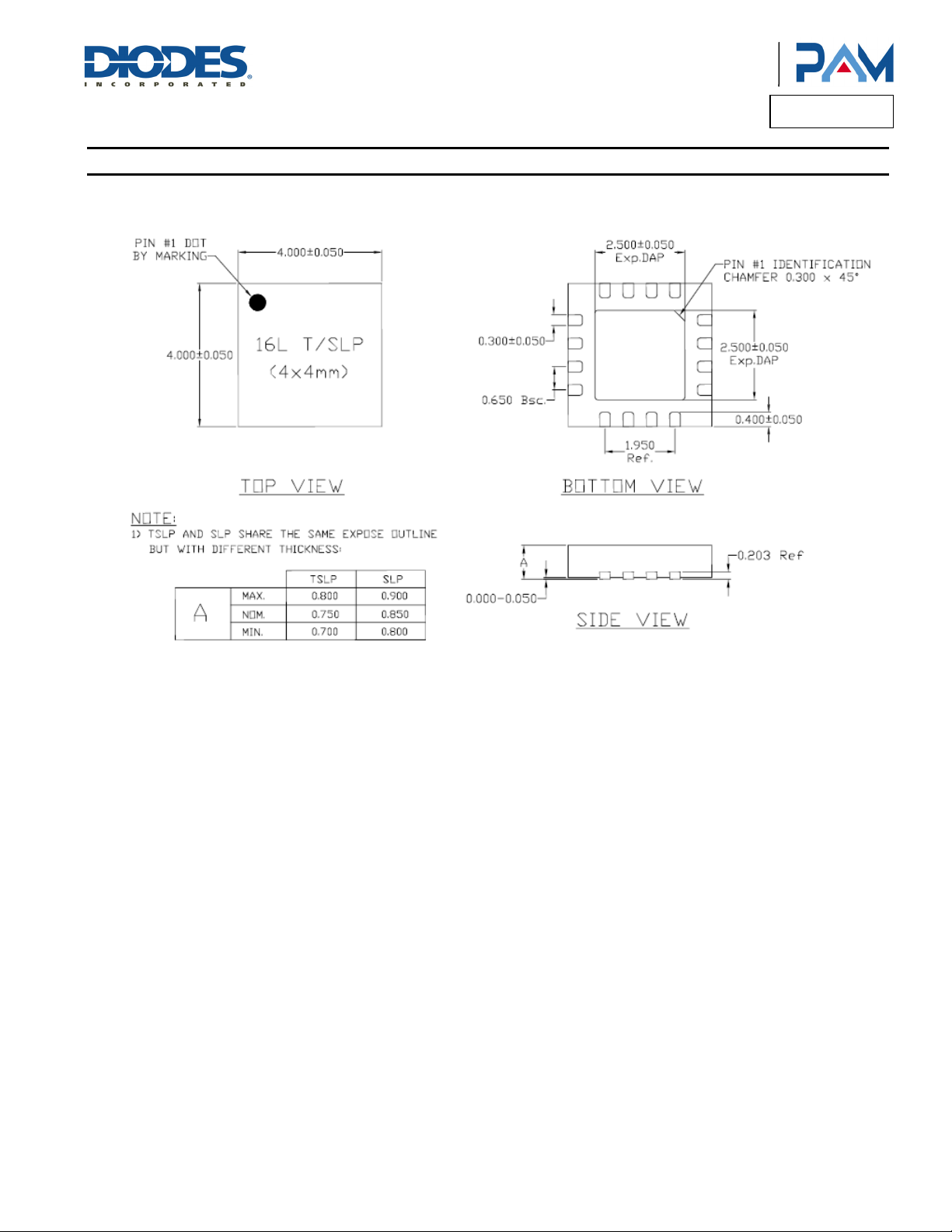
Package Outline Dimensions (cont.) (All dimensions in mm.)
QFN4x4-16
Product Line o
Diodes Incorporated
PAM8902A
PAM8902A
Document number: DSxxxxx Rev. 1 - 3
11 of 12
www.diodes.com
February 2013
© Diodes Incorporated
Page 12

A
f
Product Line o
Diodes Incorporated
PAM8902A
DIODES INCORPORATED MAKES NO WARRANTY OF ANY KIND, EXPRESS OR IMPLIED, WITH REGARDS TO THIS DOCUMENT,
INCLUDING, BUT NOT LIMITED TO, THE IMPLIED WARRANTIES OF MERCHANTABILITY AND FITNESS FOR A PARTICULAR PURPOSE
(AND THEIR EQUIVALENTS UNDER THE LAWS OF ANY JURISDICTION).
Diodes Incorporated and its subsidiaries reserve the right to make modifications, enhancements, improvements, corrections or other changes
without further notice to this document and any product described herein. Diodes Incorporated does not assume any liability arising out of the
application or use of this document or any product described herein; neither does Diodes Incorporated convey any license under its patent or
trademark rights, nor the rights of others. Any Customer or user of this document or products described herein in such applications shall assume
all risks of such use and will agree to hold Diodes Incorporated and all the companies whose products are represented on Diodes Incorporated
website, harmless against all damages.
Diodes Incorporated does not warrant or accept any liability whatsoever in respect of any products purchased through unauthorized sales channel.
Should Customers purchase or use Diodes Incorporated products for any unintended or unauthorized application, Customers shall indemnify and
hold Diodes Incorporated and its representatives harmless against all claims, damages, expenses, and attorney fees arising out of, directly or
indirectly, any claim of personal injury or death associated with such unintended or unauthorized application.
Products described herein may be covered by one or more United States, international or foreign patents pending. Product names and markings
noted herein may also be covered by one or more United States, international or foreign trademarks.
This document is written in English but may be translated into multiple languages for reference. Only the English version of this document is the
final and determinative format released by Diodes Incorporated.
Diodes Incorporated products are specifically not authorized for use as critical components in life support devices or systems without the express
written approval of the Chief Executive Officer of Diodes Incorporated. As used herein:
A. Life support devices or systems are devices or systems which:
1. are intended to implant into the body, or
2. support or sustain life and whose failure to perform when properly used in accordance with instructions for use provided in the
labeling can be reasonably expected to result in significant injury to the user.
B. A critical component is any component in a life support device or system whose failure to perform can be reasonably expected to cause the
failure of the life support device or to affect its safety or effectiveness.
Customers represent that they have all necessary expertise in the safety and regulatory ramifications of their life support devices or systems, and
acknowledge and agree that they are solely responsible for all legal, regulatory and safety-related requirements concerning their products and any
use of Diodes Incorporated products in such safety-critical, life support devices or systems, notwithstanding any devices- or systems-related
information or support that may be provided by Diodes Incorporated. Further, Customers must fully indemnify Diodes Incorporated and its
representatives against any damages arising out of the use of Diodes Incorporated products in such safety-critical, life support devices or systems.
Copyright © 2013, Diodes Incorporated
www.diodes.com
IMPORTANT NOTICE
LIFE SUPPORT
PAM8902A
Document number: DSxxxxx Rev. 1 - 3
12 of 12
www.diodes.com
February 2013
© Diodes Incorporated
 Loading...