

Page 1
p
A PRODUCT LINE OF
DIODES INCORPORATED
2x3W Stereo Differential Input Class D Audio Amplifier
Description
The PAM8407 is a filter-less Class-D amplifier with high SNR and
differential input that helps eliminate noise. Advanced 32-step
Up/Down volume control minimizes external components and allows
speaker volume control.
The PAM8407 supports 2.5V to 6V operation make it idea for up to 4
cells alkaline battery applications.
Features like greater than 87% efficiency and small PCB area make
the PAM8407 Class-D amplifier ideal for portable applications. The
output uses a filter-less architecture minimizing the number of
external components and PCB area whilst providing a high
performance, simple and lower cost system.
The PAM8407 built in auto recovery SCP (short circuit protection) and
thermal shutdown.
The PAM8407 is available in SO-16 package.
New Product
Features
3W Output at 10% THD with a 4Ω load and 5V Supply
2.4W Output at 1% THD with a 4Ω Load and 5V Supply
2.5V to 6.0V VDD Operating
Fully Differential Input
Filterless, Low Quiescent Current and Low EMI
Low THD+N
32-stepUp/Down Volume Control from -80dB to 24dB
Superior Low Noise: 60uV
Minimize Pop/Clip Noise
Auto Recovery Short Circuit Protection
Thermal Shutdown
Pb-Free SO-16 Package
with U
/Down Volume Control
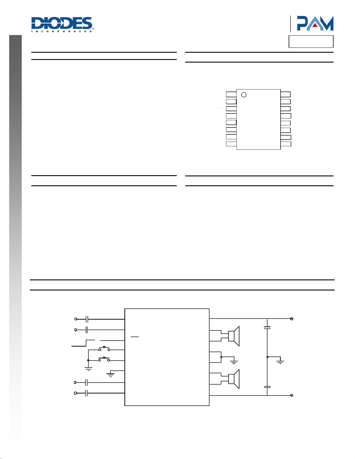
Pin Assignments
RINP
RINN
SD
UP
DOWN
GND
LINN
LINP
Applications
PC Speaker
Wireless Speaker
Home Sound Systems
Active Speakers
Docking stations
PAM8407
SO-16
1
2
3
4
5
6
7
8
XXXYW WLL
PAM8407
16
15
14
13
12
11
10
9
VDD
ROUTP
ROUTN
GND
GND
LOUTN
LOUTP
VDD
Typical Applications Circuit
RINP
RINN
SHDN
LINN
LINP
C5
01. uF
C6
01. uF
ON
C7
01. uF
C8
01.
PAM8407
Document number: DS36815 Rev. 1 - 2
uF
1 RINP
2 RINN
3 SD
4 UP
5 DOWN
6 GND
7 LINN
8 LINP
PAM8407
www.diodes.com
VDD 16
ROUTP 15
ROUTN 14
GND 13
GND 12
LOUTN 11
LOUTP 10
1 of 12
VDD 9
4Ω
4Ω
C2
1uF
C2
1uF
V
DD
V
DD
January 2014
© Diodes Incorporated
Page 2
p
A PRODUCT LINE OF
DIODES INCORPORATED
Pin Descriptions
PIN Number PIN Name Description
1 RINP Positive Input of Right Channel Power Amplifier.
2 RINN Negative Input of Right Channel Power Amplifier.
3 SD Full Chip Shutdown Control Input (active low).
4 UP Volume UP Control (active low)Ground Connection.
5 DOWN Volume down Control (active low)
6,12,13 GND Ground.
7 LINN Negative Input of Left Channel Power Amplifier.
8 LINP Positive Input of Left Channel Power Amplifier.
New Product
9,16 VDD Power Supply.
10 LOUTP Positive Output of Left Channel Power Amplifier.
11 LOUTN Negative Output of Left Channel Power Amplifier.
14 ROUTN Negative Output of Right Channel Power Amplifier.
15 ROUTP Positive Output of Right Channel Power Amplifier.
Functional Block Diagram
2x3W Stereo Differential Input Class D Audio Amplifier
with U
/Down Volume Control
PAM8407
VDD
GND
RINP
RINN
VDD
UP
VDD
DOW N
LIN N
LINP
VDD
Absolute Maximum Ratings (@T
In terf ac e Co n tro l
= +25°C, unless otherwise specified.)
A
+
-
Attenuation Decoder
OSCILLATOR
OSC
+
-
Parameter Rating Unit
Supply Voltage (VDD) 6.5
Pins Input Voltage (SD, UP, Down, IN) -0.3 to VDD+0.3
Storage Temperature -65 to +150
Maximum Junction Temperature +150
Junction to ambient thermal resistance 40
MODULATOR
INTERNAL
MODUL ATO R
DRIVER
Thermal
Protection
BIAS
AND
REFERE NCES
Current
Protection
DRIVER
GND
ROUTP
ROUTN
VDD
SD
LOUT N
LOUT P
V
V
°C
°C
°C/W
PAM8407
Document number: DS36815 Rev. 1 - 2
2 of 12
www.diodes.com
January 2014
© Diodes Incorporated
Page 3
p
A PRODUCT LINE OF
DIODES INCORPORATED
2x3W Stereo Differential Input Class D Audio Amplifier
with U
/Down Volume Control
Recommended Operating Conditions (@T
= +25°C, unless otherwise specified.)
A
Symbol Parameter Min Max Unit
VDD
TA
TJ
Operating Ambient Temperature Range -40 +85 °C
Supply Voltage 2.5 6.0 V
Junction Temperature Range -40 +125 °C
Electrical Characteristics (@TA=25°C, VDD=5.0V, Gain=24dB, RL=8Ω (33μH)+R+L(33μH), unless otherwise noted.)
PARAMETER SYMBOL CONDITIONS MIN TYP MAX UNITS
New Product
Supply Voltage Range
Quiescent Current
Output Offset Voltage
Drain-Source On-State
Resistance
V
V
R
DS(ON)
I
— 2.5 — 5.5 V
DD
No Load —
Q
No Load —
OS
I
DS
= 0.5A
P MOSFET —
N MOSFET — 0.2 —
PAM8407
8 — mA
10 — mV
0.3 —
Ω
1.4 —
R
= 8Ω
Output Power
Total Harmonic Distortion Plus
Noise
Power Supply Ripple Rejection PSRR Input AC-GND, f = 1KHz, Vpp = 200mV — 70 — dB
Channel Separation CS
Oscillator Frequency
Efficiency η
Noise Vn
Signal Noise Ratio SNR f = 20-20kHz, THD = 1% — 95 — dB
Turn-on Time Ton VDD = 5V — 0.65 — S
Mute Current
Shutdown Current
Logic Input High
Logic Input Low
Over Temperature Protection OTP — — 150 — °C
P
THD+N
f
OSC
I
MUTE
I
SD
V
V
THD+N = 1%,
O
f = 1kHz
= 8Ω,PO = 0.85W, f = 1KHz
R
L
RL = 4Ω,PO = 1.75W, f = 1KHz
P
= 1W, f = 1KHz
O
— 200 250 300 kHz
P
= 1.1W,f = 1kHz, RL = 8Ω
O
PO = 2.4W,f = 1kHz, RL = 4Ω
Input
AC-GND
MUTE = VDD — 4 10 mA
V
IH
IL
= 0V
SD
Include SD, UP, DOWN 1.4 — — V
Include SD, UP, DOWN — — 0.6 V
L
RL = 4Ω
A-weighting — 60 —
No A-weighting — 80 —
—
2.4 —
—
—
0.08 —
—
0.08 —
-95 — dB
—
— 87 — %
— 83 — %
— — 1 µA
W
%
μV
Over Temperature Hysteresis OTH — — 40 — °C
PAM8407
Document number: DS36815 Rev. 1 - 2
3 of 12
www.diodes.com
January 2014
© Diodes Incorporated
Page 4
p
A PRODUCT LINE OF
DIODES INCORPORATED
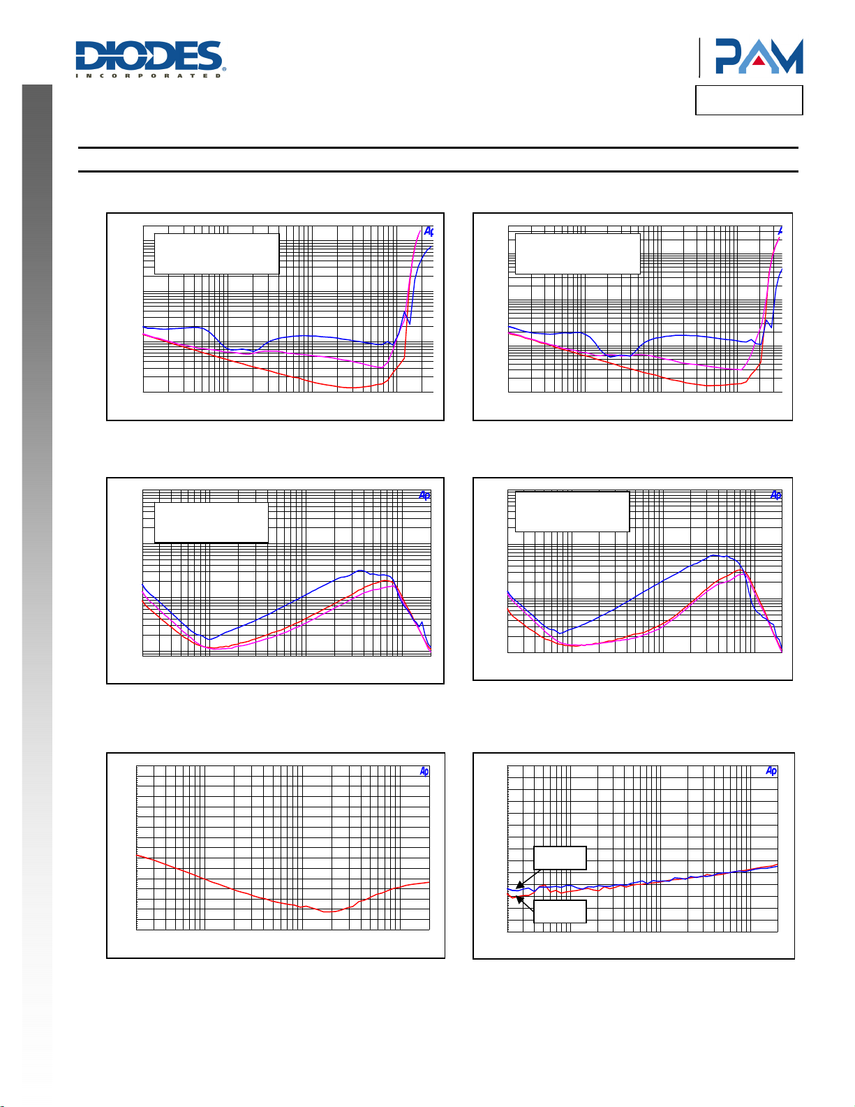
Performance Characteristics (@T
THD+N Vs. Output Power (RL=8Ω) THD+N Vs. Output Power (RL=4Ω)
20
10
f=100Hz/1kHz/10kHz
5
(Red/Pink/Blue)
2
1
0.5
%
0.2
0.1
0.05
0.02
0.01
1m 2m 5m 10m 20m 50m 100m 200m 500m 1 2
New Product
PAM8407
Document number: DS36815 Rev. 1 - 2
THD+N Vs. Frequency (RL=8Ω) THD+N Vs. Frequency (RL=4Ω)
10
5
2
1
0.5
%
0.2
0.1
0.05
0.02
0.008
20 20k50 100 200 500 1k 2k 5k 10k
PO=0.3W/0.5W/1W
(Red/Pink/Blue)
PSRR Vs. Frequency Crosstalk Vs Frequency
+0
-5
-10
-15
-20
-25
-30
-35
d
-40
B
-45
-50
-55
-60
-65
-70
-75
-80
20 20k50 100 200 500 1k 2k 5k 10k
2x3W Stereo Differential Input Class D Audio Amplifier
with U
= +25°C, V
A
W
Hz
Hz
= 5V, Gain = 24dB, RL = L(33μH) + R + L(33μH), unless otherwise noted.)
DD
%
%
d
B
4 of 12
www.diodes.com
/Down Volume Control
40
20
f=100Hz/1kHz/10kHz
10
(Red/Pink/Blue)
5
2
1
0.5
0.2
0.1
0.05
0.02
0.01
1m 2m 5m 10m 20m 50m 100m 200m 500m 1 2
10
PO=0.5W/1W/2W
5
(Red/Pink/Blue)
2
1
0.5
0.2
0.1
0.05
0.02
0.01
20 20k50 100 200 500 1k 2k 5k 10k
+0
-10
-20
-30
-40
-50
-60
-70
-80
-90
-100
-110
-120
-130
-140
T
L to R
R to L
20 20k50 100 200 500 1k 2k 5k 10k
PAM8407
W
Hz
Hz
January 2014
© Diodes Incorporated
Page 5

p
A PRODUCT LINE OF
DIODES INCORPORATED
Performance Characteristics
Frequency Response Noise Floor
New Product
PAM8407
Document number: DS36815 Rev. 1 - 2
+16
+14
+12
+10
d
B
g
A
Cin=0.1uF
+8
+6
+4
+2
+0
20 20k50 100 200 500 1k 2k 5k 10k
Efficiency Vs. Output Power (RL=8Ω) Efficiency Vs. Output Power (RL=4Ω)
100
80
60
40
20
Efficiency(%)
0
0 200 400 600 800 10001200140016001800
Output Power Vs. Supply Voltage (RL=8Ω, THD=10%) Output Power Vs. Supply Voltage(RL=4Ω,THD=10%)
2500
2000
1500
1000
500
0
23456
OutputPower(mW)
2x3W Stereo Differential Input Class D Audio Amplifier
(@T
= +25°C, V
A
Cin=1uF Cin=0.47uF
Hz
VDD=5V VDD=5V
OutputPower(mW)
InputVoltage(V)
with U
= 5V, Gain = 24dB, RL = L(33μH) + R + L(33μH), unless otherwise noted.)
DD
d
B
r
A
100
4000
3000
2000
1000
5 of 12
www.diodes.com
/Down Volume Control
+0
-10
-20
-30
-40
-50
-60
-70
-80
-90
-100
-110
-120
-130
-140
20 20k50 100 200 500 1k 2k 5k 10k
Hz
80
60
40
20
Efficiency(%)
0
0 1000 2000 3000 4000
OutputPower(mW)
0
23456
OutputPower(mW)
InputVoltage(V)
January 2014
© Diodes Incorporated
PAM8407
Page 6
p
A PRODUCT LINE OF
DIODES INCORPORATED
Performance Characteristics (@T
Quiescent Current Vs. Supply Voltage OSC Frequency Vs. Supply Voltage
10
9
8
7
6
5
Quiescent
4
Current(mA)
3
23456
New Product
400
350
300
250
200
150
100
50
Rdson(mohm)
0
0 500 1000 1500
SupplyVoltage(V)
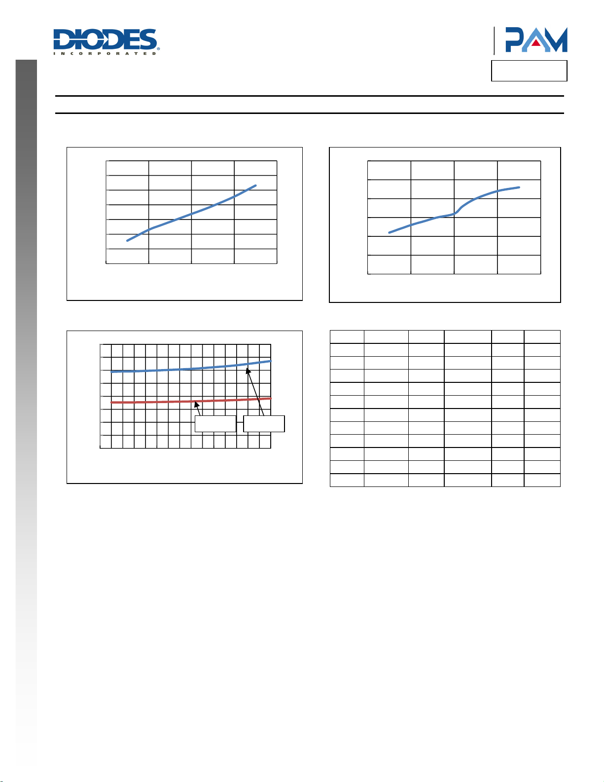
Rdson Vs. Output Current Up/Down Volume Control (dB)
OutputCurrent(mA)
2x3W Stereo Differential Input Class D Audio Amplifier
= +25°C, V
A
with U
= 5V, Gain = 24dB, RL = L(33μH) + R + L(33μH), unless otherwise noted.)
DD
/Down Volume Control
270
265
260
255
250
245
240
PMOS NMOS
Frequency(kHz)
23456
STEP Gain STEP Gain STEP Gain
1 24 12 7.5
2 22.5 13 6
3 21 14 4.5
4 19.5 15 3
5 18 16 1.5
6 16.5 17 0
7 15 18 -1.5
8 13.5 19 -3
9 12* 20 -4.5
10 10.36 21 -6
11 9 22 -8
*Default Gain=12dB
SupplyVoltage(V)
PAM8407
23
24
25
26
27
28
29
30
31
32
-
-10
-12
-14
-16
-18
-20
-22
-24
-26
-80
-
PAM8407
Document number: DS36815 Rev. 1 - 2
6 of 12
www.diodes.com
January 2014
© Diodes Incorporated
Page 7

p
A PRODUCT LINE OF
DIODES INCORPORATED
2x3W Stereo Differential Input Class D Audio Amplifier
with U
/Down Volume Control
PAM8407
Application Information
Maximum Gain
As shown in block diagram, the PAM8407 has two internal amplifiers stage. The first stage's gain is externally con-figurable, while the second
stage's is internally fixed in a fixed-gain, inverting configuration. The closed-loop gain of the first stage is set by selecting the ratio of Rf to Ri while
the second stage's gain is fixed at 2x. Consequently, the differential gain for the IC is
The PAM8407 sets maximum Rf=218kΩ and minimum Ri=27kΩ, thus the maximum closed-gain is 24dB.
UP/DOWN Volume Control (DVC)
The PAM8407 features a UP/DOWN volume control which consists of the UP and DOWN pins. An internal clock is used where the clock
frequency value is determined from the following formula:
New Product
The oscillator frequency f
Volume changes are then effected by toggling either the UP or DOWN pins with a logic low. After a period of 1 cycle pulses with either the UP or
DOWN pins held low, the volume will change to the next specified step, either UP or DOWN, and followed by a short delay. This delay decreases
the longer the line is held low, eventually reaching a delay of zero. The delay allows the user to pull the UP or DOWN terminal low once for one
volume change, or hold down to ramp several volume changes. The delay is optimally configured for push button volume control.
If either the UP or DOWN pin remains low after the first volume transition the volume will change again, but this time after 10 cycles. The followed
transition occurs at 4 cycles for each volume transition. This is intended to provide the user with a volume control that pauses briefly after initial
application, and then slowly increases the rate of volume change as it is continuously applied. This cycle is shown in the timing diagram shown in
figure 1.
There are 32 discrete gain settings ranging from +24dB maximum to -80dB minimum. Upon device power on or applied a logic low to the SD pin,
the amplifier's gain is set to a default value of 12dB. Volume levels for each step vary and are specified in Gain Setting table on page 7.
If both the UP and DOWN pins are held high, no volume change will occur. Trigger points for the UP and DOWN pins are at 70% of VDD minimum
for a logic high, and 20% of VDD maximum for a logic low. It is recommended, however, to toggle UP and DOWN between VDD and GND for best
performance.
value is 250kHz typical,with ±20% tolerance. The DVC’s clock frequency is 30Hz (cycle time 33ms) typical.
OSC
UP/DN
A
= 20*log [2*(Rf/Ri)]
VD
f
= f
CLK
OSC
/ 2
13
VOL U ME
LEVEL
1 cycle
Shutdown operation
In order to reduce power consumption while not in use, the PAM8407 contains shutdown circuitry that is used to turn off the amplifier's bias
circuitry. This shutdown feature turns the amplifier off when logic low is placed on the SD pin. By switching the SD pin connected to GND, the
PAM8407 supply current draw will be minimized in idle mode. The SD pin cannot be left floating due to the pull-down internal.
10 cycles 4 cycles
Figure 1.Timming Diagram
4 cycles
PAM8407
Document number: DS36815 Rev. 1 - 2
7 of 12
www.diodes.com
January 2014
© Diodes Incorporated
Page 8

p
A PRODUCT LINE OF
DIODES INCORPORATED
2x3W Stereo Differential Input Class D Audio Amplifier
with U
/Down Volume Control
PAM8407
Application Information
(Continued)
Power supply decoupling
The PAM8407 is a high performance CMOS audio amplifier that requires adequate power supply decoupling to ensure the output THD and PSRR
are as low as possible. Power supply decoupling is affecting low frequency response. Optimum decoupling is achieved by using two capacitors of
different types that target different types of noise on the power supply leads. For higher frequency transients, spikes, or digital hash on the line, a
good low equivalent-series-resistance (ESR) ceramic capacitor, typically 1.0µF, placed as close as possible to the device VDD terminal works best.
For filtering lower-frequency noise signals, a larger capacitor of 10µF (ceramic) or greater placed near the audio power amplifier is recommended.
Input Capacitor (Ci)
Large input capacitors are both expensive and space hungry for portable designs. Clearly, a certain sized capacitor is needed to couple in low
frequencies without severe attenu-ation. But in many cases the speakers used in portable systems, whether internal or external, have little ability
to reproduce signals below 100Hz to 150Hz. Thus, using a large input capacitor may not increase actual system perfor-mance. In this case, input
capacitor (Ci) and input resistance (Ri) of the amplifier form a high-pass filter with the corner frequency determined equation below,
New Product
In addition to system cost and size, click and pop perfor-mance is affected by the size of the input coupling capacitor, Ci. A larger input coupling
capacitor requires more charge to reach its quiescent DC voltage (nominally 1/2 VDD). This charge comes from the internal circuit via the
feedback and is apt to create pops upon device enable. Thus, by minimizing the capacitor size based on necessary low frequency response, turnon pops can be minimized.
Under Voltage Lock-out (UVLO)
The PAM8407 incorporates circuitry designed to detect when the supply voltage is low. When the supply voltage drops to 2.4V or below, the
PAM8407 outputs are disable, and the device comes out of this state and starts to normal functional when the supply voltage increases.
Short Circuit Protection (SCP)
The PAM8407 has short circuit protection circuitry on the outputs that prevents damage to the device during output-to-output and output-to-GND
short. When a short circuit is detected on the outputs, the outputs are disable immediately. If the short was removed, the device activates again.
Over Temperature Protection
Thermal protection on the PAM8407 prevents damage to the device when the internal die temperature exceeds 150°C. There is a 15 degree
tolerance on this trip point from device to device. Once the die temperature exceeds the thermal set point, the device outputs are disabled. This is
not a latched fault. The thermal fault is cleared once the temperature of the die is reduced by 60°C. This large hysteresis will prevent motor
boating sound well and the device begins normal operation at this point with no external system interaction.
How to Reduce EMI (Electro Magnetic Interference)
A simple solution is to put an additional capacitor 1000uF at power supply terminal for power line coupling if the traces from amplifier to speakers
are short (<20cm). Most applications require a ferrite bead filter which shows at Figure 3. The ferrite filter reduces EMI around 1 MHz and higher.
When selecting a ferrite bead, choose one with high impedance at high frequencies, but low impedance at low frequencies.
f=
C
1
2πRC
ii
PAM8407
Document number: DS36815 Rev. 1 - 2
8 of 12
www.diodes.com
© Diodes Incorporated
January 2014
Page 9

p
A PRODUCT LINE OF
DIODES INCORPORATED
2x3W Stereo Differential Input Class D Audio Amplifier
with U
/Down Volume Control
PAM8407
Application Information
(Continued)
Ferrite Bead
OUT+
220pF
Ferrite Bead
OUT-
220pF
New Product
Figure 3: Ferrite Bead Filter to reduce EMI
PCB Layout Guidelines
Grounding
At this stage it is paramount that we acknowledge the need for separate grounds. Noise currents in the output power stage need to be returned to
output noise ground and nowhere else. Were these currents to circulate elsewhere, they may get into the power supply, the signal ground, etc,
worse yet, they may form a loop and radiate noise. Any of these instances results in degraded amplifier performance. The logical returns for the
output noise currents associated with Class D switching are the respective PGND pins for each channel. The switch state diagram illustrates that
PGND is instrumental in nearly every switch state. This is the perfect point to which the output noise ground trace should return. Also note that
output noise ground is channel specific. A two channels amplifier has two mutually exclusive channels and consequently must have two mutually
exclusive output noise ground traces. The layout of the PAM8407 offers separate PGND connections for each channel and in some cases each
side of the bridge. Output noise grounds must tie to system ground at the power in exclusively. Signal currents for the inputs, reference, etc need
to be returned to quite ground. This ground only ties to the signal components and the GND pin. GND then ties to system ground.
Power Supply Line
As same to the ground, VDD and each channel PVDD need to be separated and tied together at the system power supply. Recommend that all
the trace could be routed as short and thick as possible. For the power line layout, just imagine water stream, any barricade placed in the trace
(shows in figure 4) could result in the bad performance of the amplifier.
Figure 4
Components Placement
The power supply decoupling capacitors need to be placed as close to VDD pins as possible. The inputs need to be routed away from the noisy
trace.
PAM8407
Document number: DS36815 Rev. 1 - 2
9 of 12
www.diodes.com
January 2014
© Diodes Incorporated
Page 10

p
A PRODUCT LINE OF
DIODES INCORPORATED
Ordering Information
Part Number Package Standard Package
PAM8407DR SO-16 2,500Units/Tape&Real
D: SO-16 R: Tape & Real
New Product
Marking Information
RINP
DOWN
GND
2x3W Stereo Differential Input Class D Audio Amplifier
with U
/Down Volume Control
PAM8407 X X
Package Type
1
2
RINN
3
SD
4
UP
5
6
LINN
7
LINP
8
16
XXXYW WLL
PAM8407
15
14
13
12
11
10
9
VDD
ROUTP
ROUTN
GND
GND
LOUTN
LOUTP
VDD
Shipping Package
PAM8407: Product Code
X: Internal Code
Y: Year
W: Week
LL: Internal Code
PAM8407
PAM8407
Document number: DS36815 Rev. 1 - 2
10 of 12
www.diodes.com
January 2014
© Diodes Incorporated
Page 11

p
A PRODUCT LINE OF
DIODES INCORPORATED
2x3W Stereo Differential Input Class D Audio Amplifier
Package Outline Dimensions (All dimensions in mm.)
Please see AP02002 at http://www.diodes.com/datasheets/ap02002.pdf for latest version.
Package:
SO-16
H
E
L
Detail ‘A’
Detail ‘A’
New Product
B
D
A
A2
e
A1
C
Suggested Pad Layout (All dimensions in mm.)
Please see AP02001 at http://www.diodes.com/datasheets/ap02001.pdf for the latest version.
X1
with U
Gauge Plane
/Down Volume Control
Dim Min Max
SO-16
A 1.40 1.75
A1 0.10 0.25
A2 1.30 1.50
B 0.33 0.51
C 0.19 0.25
D 9.80 10.00
E 3.80 4.00
e 1.27 Typ
H 5.80 6.20
L 0.38 1.27
0 8
All Dimensions in mm
PAM8407
Dimensions
C 1.270
X 0.670
Y1
Y
Pin 1
X
PAM8407
Document number: DS36815 Rev. 1 - 2
C
11 of 12
www.diodes.com
X1 9.560
Y 1.450
Y1 6.400
Value
(in mm)
January 2014
© Diodes Incorporated
Page 12

p
A PRODUCT LINE OF
DIODES INCORPORATED
2x3W Stereo Differential Input Class D Audio Amplifier
with U
DIODES INCORPORATED MAKES NO WARRANTY OF ANY KIND, EXPRESS OR IMPLIED, WITH REGARDS TO THIS DOCUMENT,
INCLUDING, BUT NOT LIMITED TO, THE IMPLIED WARRANTIES OF MERCHANTABILITY AND FITNESS FOR A PARTICULAR PURPOSE
(AND THEIR EQUIVALENTS UNDER THE LAWS OF ANY JURISDICTION).
Diodes Incorporated and its subsidiaries reserve the right to make modifications, enhancements, improvements, corrections or other changes
without further notice to this document and any product described herein. Diodes Incorporated does not assume any liability arising out of the
application or use of this document or any product described herein; neither does Diodes Incorporated convey any license under its patent or
trademark rights, nor the rights of others. Any Customer or user of this document or products described herein in such applications shall assume
all risks of such use and will agree to hold Diodes Incorporated and all the companies whose products are represented on Diodes Incorporated
website, harmless against all damages.
Diodes Incorporated does not warrant or accept any liability whatsoever in respect of any products purchased through unauthorized sales channel.
Should Customers purchase or use Diodes Incorporated products for any unintended or unauthorized application, Customers shall indemnify and
hold Diodes Incorporated and its representatives harmless against all claims, damages, expenses, and attorney fees arising out of, directly or
indirectly, any claim of personal injury or death associated with such unintended or unauthorized application.
Products described herein may be covered by one or more United States, international or foreign patents pending. Product names and markings
noted herein may also be covered by one or more United States, international or foreign trademarks.
New Product
This document is written in English but may be translated into multiple languages for reference. Only the English version of this document is the
final and determinative format released by Diodes Incorporated.
Diodes Incorporated products are specifically not authorized for use as critical components in life support devices or systems without the express
written approval of the Chief Executive Officer of Diodes Incorporated. As used herein:
A. Life support devices or systems are devices or systems which:
1. are intended to implant into the body, or
labeling can be reasonably expected to result in significant injury to the user.
B. A critical component is any component in a life support device or system whose failure to perform can be reasonably expected to cause the
failure of the life support device or to affect its safety or effectiveness.
Customers represent that they have all necessary expertise in the safety and regulatory ramifications of their life support devices or systems, and
acknowledge and agree that they are solely responsible for all legal, regulatory and safety-related requirements concerning their products and any
use of Diodes Incorporated products in such safety-critical, life support devices or systems, notwithstanding any devices- or systems-related
information or support that may be provided by Diodes Incorporated. Further, Customers must fully indemnify Diodes Incorporated and its
representatives against any damages arising out of the use of Diodes Incorporated products in such safety-critical, life support devices or systems.
Copyright © 2013, Diodes Incorporated
www.diodes.com
2. support or sustain life and whose failure to perform when properly used in accordance with instructions for use provided in the
IMPORTANT NOTICE
LIFE SUPPORT
/Down Volume Control
PAM8407
PAM8407
Document number: DS36815 Rev. 1 - 2
12 of 12
www.diodes.com
January 2014
© Diodes Incorporated
 Loading...