

Page 1
A
f
Product Line o
Diodes Incorporated
PAM8010
3W STEREO CLASS-D with
DC VOLUME, HEADPHONE and POWER LIMIT
Description
The PAM8010 is a 3W, Class-D audio amplifier with headphone
amplifier. Advanced 64-step DC volume control minimizes external
components and allows speaker volume control and headphone
volume control.
Integrated power limit technology which suppresses the output signal
clip automatically due to the over level input signal. It offers low
THD+N to produce high-quality sound reproduction.
PAM8010 has an additional noise reduction circuit which achieves
12dB nosie attenuation. This circuit may help eliminate external
filtering, thereby saving the board space and component cost.
The PAM8010 features SCP (short circuit protection), OTP and
thermal shutdown.
The PAM8010 is available in SSOP-24 and SOP-24 package.
Features
3W Output at 10% THD with a 4 Load and 5V Power Supply
Filterless, Low Quiescent Current and Low EMI
Low THD+N
Power Limit Function to Protect Speaker when Occuring Large
Input, 5% Power Limit Accuracy
64-Step DC Volume Control from -45dB to +24dB
Headphone Output Function
12dB Effective Noise Reduction
Superior Low Noise: 30uV
Minimize Pop/Clip Noise
High Efficiency up to 90%
Auto Recovery Short Circuit Protection
Thermal Shutdown
Pb-Free Package
PAM8010
Document number: DSxxxxx Rev. 1 - 0
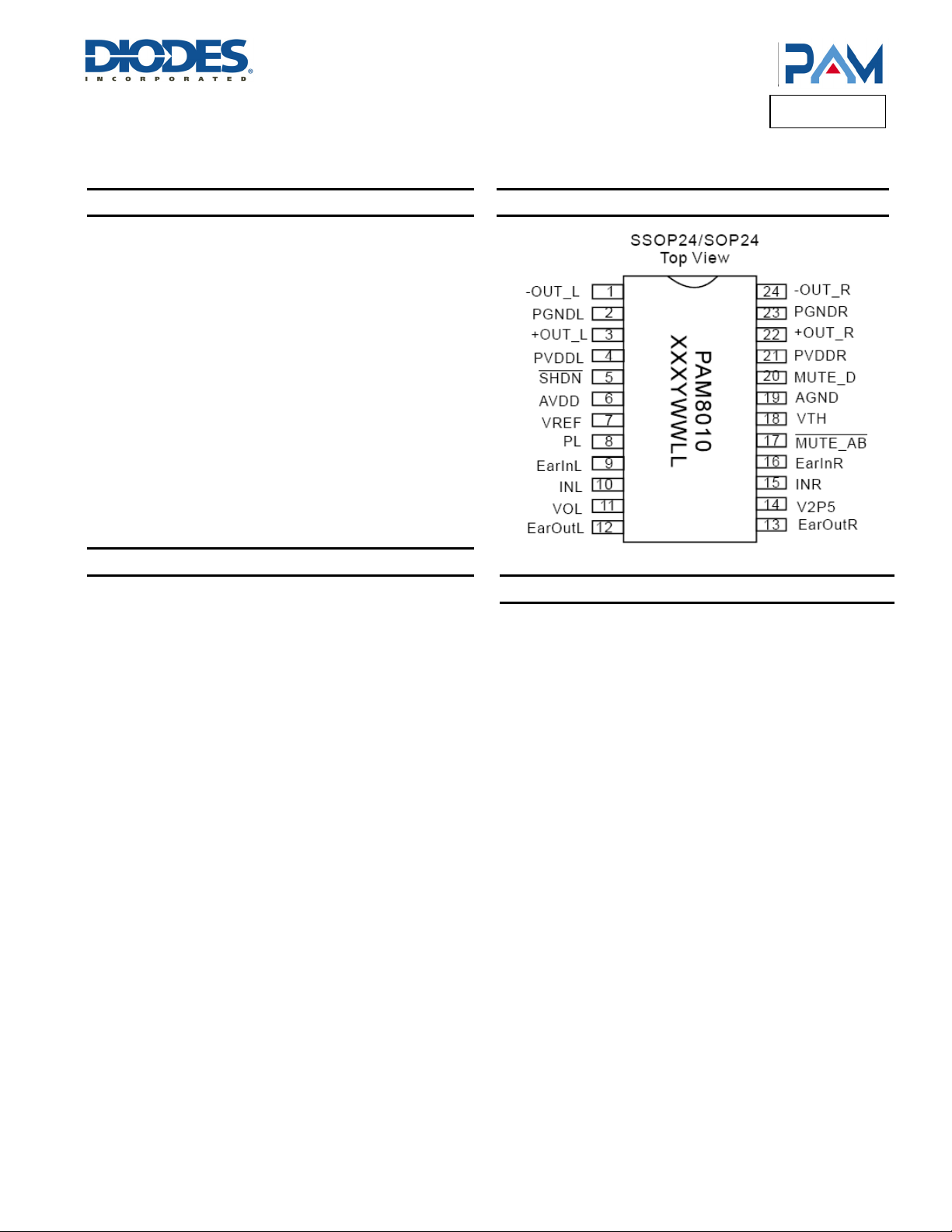
Pin Assignments
Applications
LCD Monitors / TV Projectors
Notebook/All-in-one Computers
Portable Speakers
Portable DVD Players, Game Machines
1 of 17
www.diodes.com
November 2012
© Diodes Incorporated
Page 2
A
f
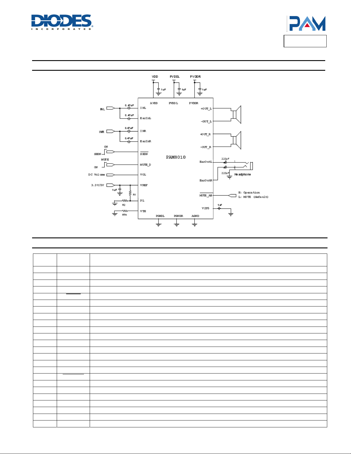
Typical Applications Circuit
Product Line o
Diodes Incorporated
PAM8010
Pin Descriptions
Pin
Number
1 -OUT_L Left Channel Negative Output
2 PGNDL Left Channel Power GND
3 +OUT_L Left Channel Positive Output
4 PVDDL Left Channel Power Supply
5 SHDN Full Chip Shutdown Control Input (active low), Pull-Up
6 AVDD Analog VDD
7 VREF Reference Voltage Both for DC Volume Control and Power Limit Section
8 PL Connect a Resistor Divider from VREF to GND for Power Limit Setting
9 EAR IN L Left Earphone Input
10 INL Left Channel Input
11 VOL Apply DC Voltage at this Pin Set the Gain Both of Class-D and Class-AB
12 EAR OUT L Left Earphone Output (Non-Inverting)
13 EAR OUT R Right Earphone Output(Non-Inverting)
14 V2P5 Internal Analog Reference, Connect a Bypass Capacitor from V2P5 to GND
15 IN R Right Channel Input
16 EAR IN R Right Earphone Input
17 MUTE_AB Mute Control of Class-AB Section (active low), Pull-Up
18 VTH Connect a Resistor from VTH to GND for Noise Threshold Setting
19 AGND Analog GND
20 MUTE_D Mute Control of Class-D Section (active high), Pull-Up
21 PVDDR Right Channel Power Supply
22 +OUT_R Right Channel Positive Output
23 PGNDR Right Channel Power GND
24 -OUT_R Right Channel Negative Output
PAM8010
Document number: DSxxxxx Rev. 1 - 0
Pin
Name
2 of 17
www.diodes.com
Function
November 2012
© Diodes Incorporated
Page 3
A
f
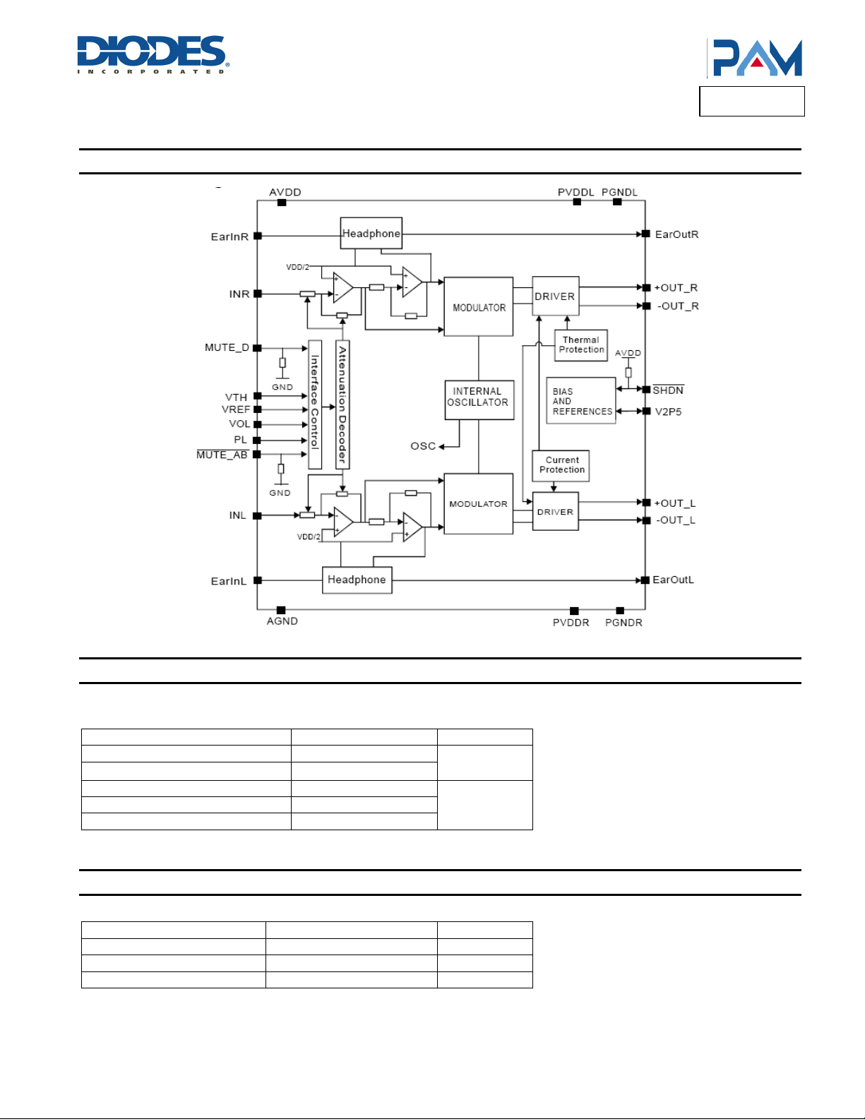
Functional Block Diagram
Product Line o
Diodes Incorporated
PAM8010
Absolute Maximum Ratings (@T
These are stress ratings only and functional operation is not implied. Exposure to absolute maximum ratings for prolonged time periods may
affect device reliability. All voltages are with respect to ground.
Parameter Rating Unit
Supply Voltage 6.0
Input Voltage
Operation Junction Temperature -40 to +125
Storage Temperature -65 to +150
Soldering Temperature 300, 5 sec
Recommended Operating Conditions (@T
Parameter Rating Unit
Supply Voltage Range 2.5 to 5.5 V
Ambient Temperature Range -20 to +85 °C
Junction Temperature Range -20 to +125 °C
PAM8010
Document number: DSxxxxx Rev. 1 - 0
= +25°C, unless otherwise specified.)
A
-0.3 to V
+0.3
DD
= +25°C, unless otherwise specified.)
A
3 of 17
www.diodes.com
V
°C
November 2012
© Diodes Incorporated
Page 4
A
f
Product Line o
Diodes Incorporated
PAM8010
Thermal Information
Parameter Package Symbol Max Unit
= 8Ω
= 200mV
PP
= 200mV
PP
96
°C/W
2.5 5.5 V
10 15 mA
Ω
1.55 1.70
2.85 3.0
0.08
0.08
W
%
70 dB
-95 dB
85 90 %
80 83 %
µV
60 mW
0.02 %
80 dB
-95 dB
µV
7 10 mA
7 10 mA
9 10 mA
1 µA
V
November 2012
© Diodes Incorporated
Thermal Resistance (Junction to Ambient)
SSOP-24
SOP-24 79.2
θ
JA
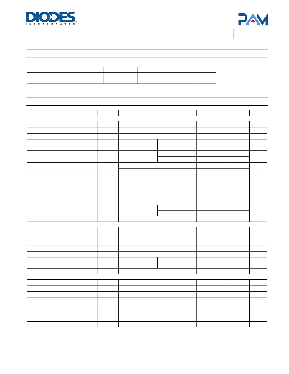
Electrical Characteristics (@T
= +25°C, VDD = 5V, Gain = Maximum, RL = 8Ω, unless otherwise specified.)
A
Parameter Symbol Test Conditions Min Typ Max Units
Class D Stage
Supply Voltage Range
Quiescent Current
Output Offset Voltage
Drain-Source On-State Resistance
Output Power
V
V
R
DS(ON)
I
P
Total Harmonic Distortion Plus Noise THD+N
Power Supply Ripple Rejection PSRR
Channel Separation CS
Oscillator Frequency
f
OSC
Efficiency η
Noise
V
DD
No Load
Q
No Load 10 30 mV
OS
IDS = 0.5A
THD+N = 10%
O
f = 1kHz
R
= 8Ω, PO = 0.85W, f = 1KHz
L
P MOSFET 0.21
N MOSFET 0.17
R
L
RL = 4Ω
RL = 4Ω, PO = 1.75W, f = 1KHz
Input AC-GND, f = 1KHz, V
P
= 1W, f = 1KHz
O
200 250 300 kHz
P
= 1.7W, f =1 kHz, RL = 8Ω
O
PO = 3.0W, f =1 kHz, RL = 4Ω
N
Input AC-GND
A-Weighting 60
No A-Weighting 80
Signal Noise Ratio SNR f = 20 – 20kHz, THD = 1% 95 dB
Earphone Stage
Output Offset Voltage
Output Power
V
P
Total Harmonic Distortion Plus Noise THD+N
Power Supply Ripple Rejection PSRR
Channel Separation CS
Noise
V
No Load 2.45 2.50 2.55 V
OS
THD+N = 1%, RL = 32Ω, f = 1KHz
O
R
= 32Ω, PO = 10mW, f = 1kHz
L
Input AC-GND, f = 1kHz, V
V
= 1V
O
Input
N
AC-GND
, f = 1kHz
RMS
A-Weighting 20
No A-Weighting 35
Signal Noise Ratio SNR f = 20 – 20kHz, THD = 1% 95 dB
Control Section
Mute Current
Mute Class-D Earphone Current
Mute Class AB EarphoneCurrent
Shutdown Current
Logic Input High
Logic Input Low
I
MUTE_D = VDD, MUTE_AB = GND
MUTE
I
MUTE_D = VDD, MUTE_AB = GND
MUTE_D
I
MUTE_D = VDD, MUTE_AB = GND
MUTE_AB
I
SHDN
V
IH
V
IL
V
= 0V
SHDN
1.4
0.6
Over Temperature Protection OTP 150 °C
Over Temperature Hysteresis OTH 40 °C
PAM8010
Document number: DSxxxxx Rev. 1 - 0
4 of 17
www.diodes.com
Page 5
A
f
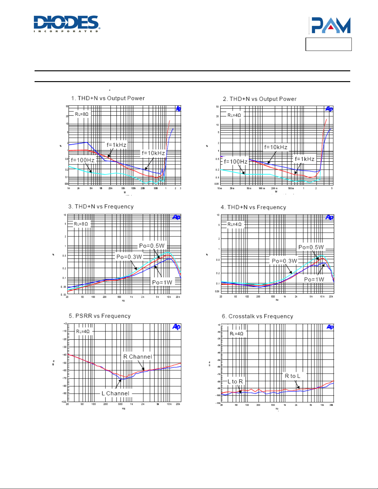
Typical Performance Characteristics (@T
Class-D Output
Product Line o
Diodes Incorporated
PAM8010
= +25°C, VDD = 5V, RL = 8Ω, GV = 24dB, unless otherwise specified.)
A
PAM8010
Document number: DSxxxxx Rev. 1 - 0
5 of 17
www.diodes.com
November 2012
© Diodes Incorporated
Page 6
A
f
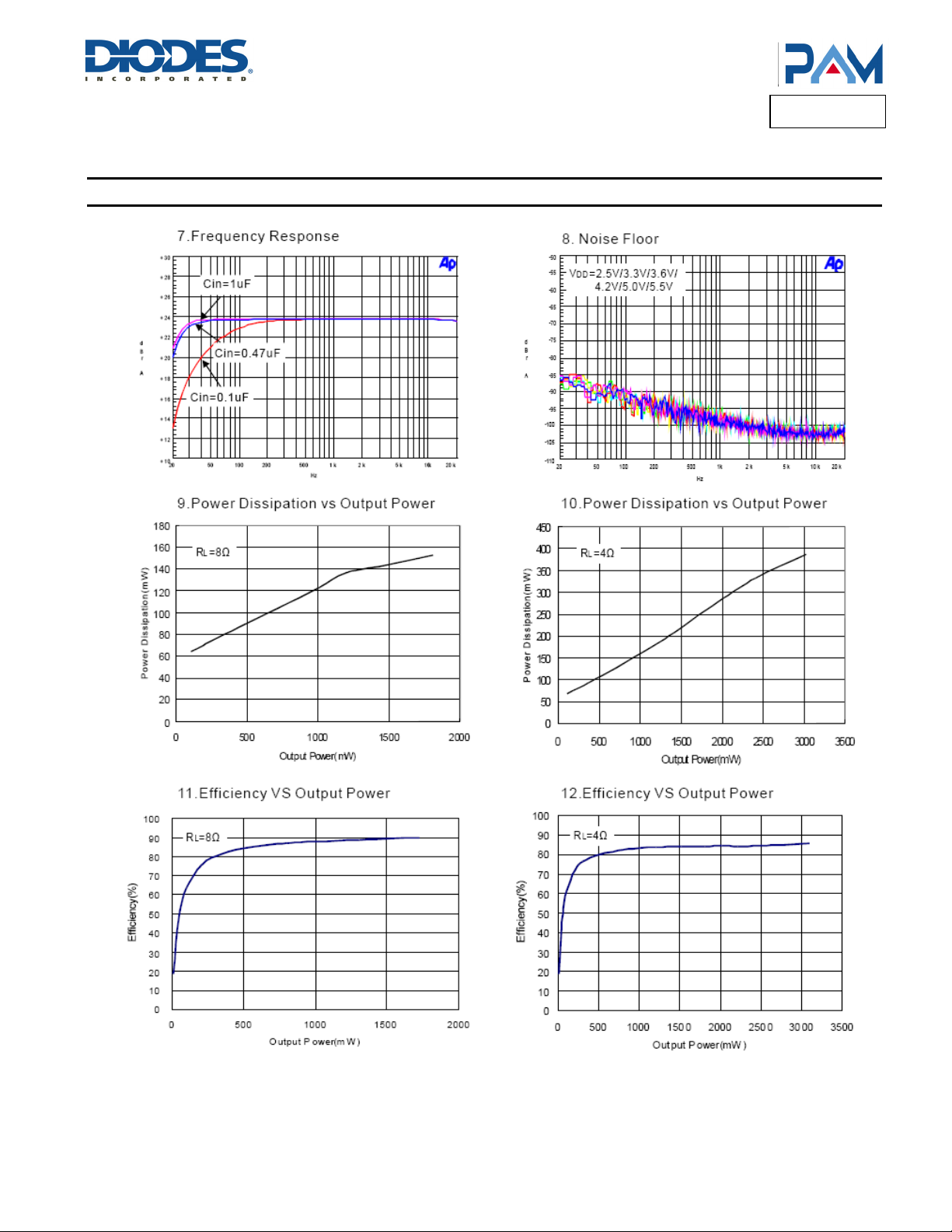
Typical Performance Characteristics (cont.) (@T
Class-D Output
Product Line o
Diodes Incorporated
PAM8010
= +25°C, VDD = 5V, RL = 8Ω, GV = 24dB, unless otherwise specified.)
A
PAM8010
Document number: DSxxxxx Rev. 1 - 0
6 of 17
www.diodes.com
November 2012
© Diodes Incorporated
Page 7
A
f
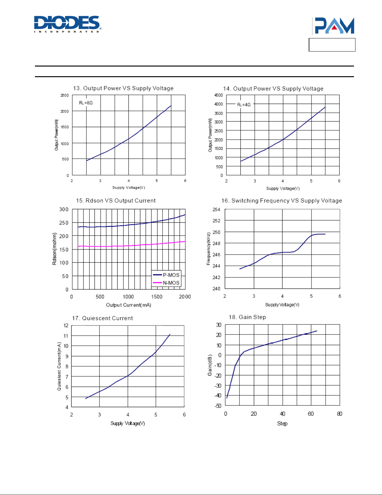
Typical Performance Characteristics (cont.) (@T
Product Line o
Diodes Incorporated
= +25°C, unless otherwise specified.)
A
PAM8010
PAM8010
Document number: DSxxxxx Rev. 1 - 0
7 of 17
www.diodes.com
November 2012
© Diodes Incorporated
Page 8
A
f
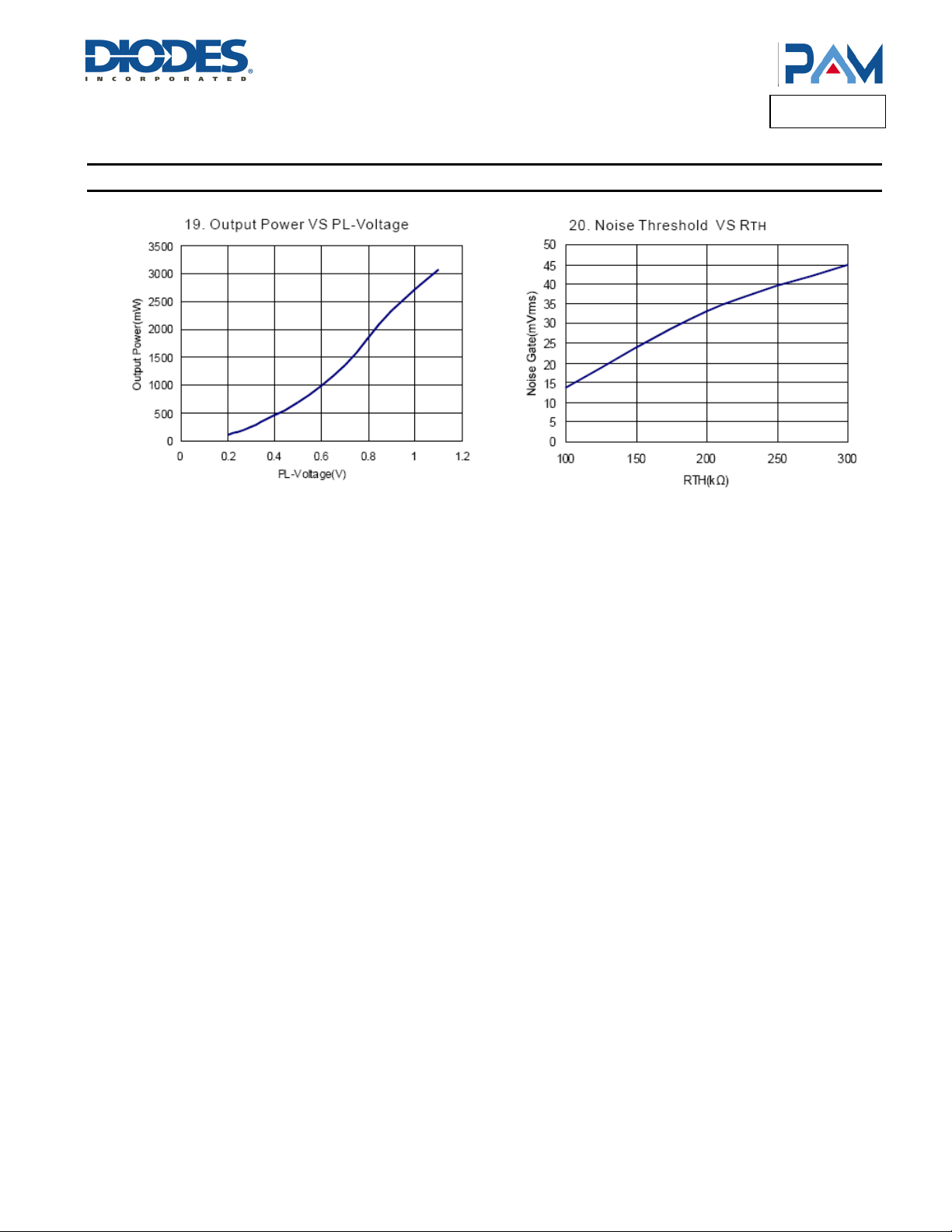
Typical Performance Characteristics (cont.) (@T
Product Line o
Diodes Incorporated
= +25°C, unless otherwise specified.)
A
PAM8010
PAM8010
Document number: DSxxxxx Rev. 1 - 0
www.diodes.com
8 of 17
November 2012
© Diodes Incorporated
Page 9
A
f
Typical Performance Characteristics (cont.) (@T
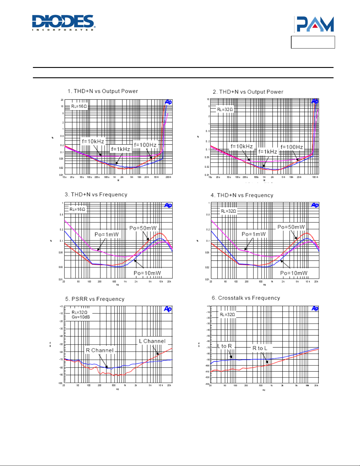
Earphone Output
Product Line o
Diodes Incorporated
PAM8010
= +25°C, VDD = 5V, GV = 10dB, unless otherwise specified.)
A
PAM8010
Document number: DSxxxxx Rev. 1 - 0
9 of 17
www.diodes.com
November 2012
© Diodes Incorporated
Page 10
A
f
Typical Performance Characteristics (cont.) (@T
Product Line o
Diodes Incorporated
PAM8010
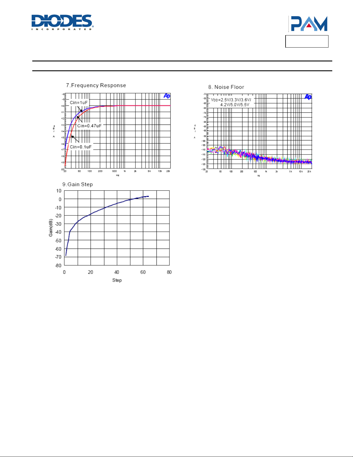
= +25°C, CIN = 10µF, CO = 10µF, L = 4.7µH, unless otherwise specified.)
A
PAM8010
Document number: DSxxxxx Rev. 1 - 0
10 of 17
www.diodes.com
November 2012
© Diodes Incorporated
Page 11
A
f
Product Line o
Diodes Incorporated
PAM8010
Typical Performance Characteristics (cont.) (@T
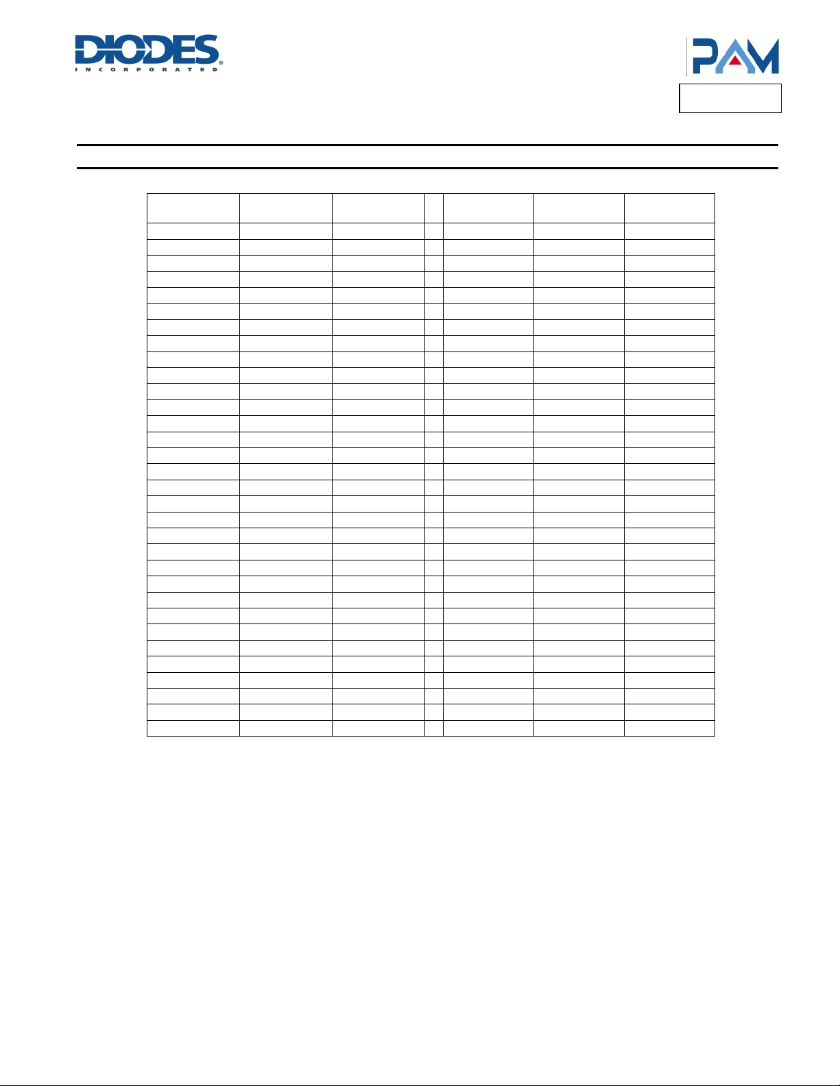
Table 1. DC Volume Control
STEP
1 -43.1 -68.5 33 11.9 -9.6
2 -37.2 -57.4 34 12.2 -9.0
3 -34.3 -49.7 35 12.7 -8.5
4 -27.7 -39.8 36 13.0 -7.9
5 -22.1 -37.4 37 13.4 -7.3
6 -16.3 -35.2 38 13.8 -6.7
7 -10.3 -33.1 39 14.2 -6.2
8 -7.8 -30.8 40 14.6 -5.7
9 -5.2 -28.7 41 15.0 -5.2
10 -2.7 -27.7 42 15.4 -4.7
11 0.2 -26.6 43 15.5 -4.2
12 1.3 -25.5 44 15.8 -3.7
13 2.8 -24.3 45 16.2 -3.2
14 3.8 -23.2 46 16.6 -2.7
15 4.2 -22.4 47 17.0 -2.3
16 4.6 -21.6 48 17.4 -1.9
17 5.4 -20.8 49 17.8 -1.5
18 5.8 -20.0 50 18.2 -1.1
19 6.2 -19.2 51 18.6 -0.7
20 6.6 -18.4 52 19.0 -0.32
21 7.0 -17.6 53 19.4 0.09
22 7.4 -16.7 54 19.8 0.4
23 7.8 -16.1 55 20.2 0.7
24 8.2 -15.4 56 20.6 0.97
25 8.6 -14.7 57 21.0 1.3
26 9.0 -14.1 58 21.4 1.6
27 9.4 -13.4 59 21.9 1.9
28 9.8 -12.7 60 22.2 2.2
29 10.3 -12.1 61 22.6 2.35
30 10.5 -11.4 62 23.1 2.6
31 11.0 -10.8 63 23.5 2.8
32 11.5 -10.2 64 23.9 3.0
Gain (dB)
Class D
PAM8010
Document number: DSxxxxx Rev. 1 - 0
Gain (dB)
Earphone
= +25°C, unless otherwise specified.)
A
11 of 17
www.diodes.com
STEP
Gain (dB)
Class D
Gain (dB)
Earphone
November 2012
© Diodes Incorporated
Page 12
A
f
Product Line o
Diodes Incorporated
PAM8010
Application Information
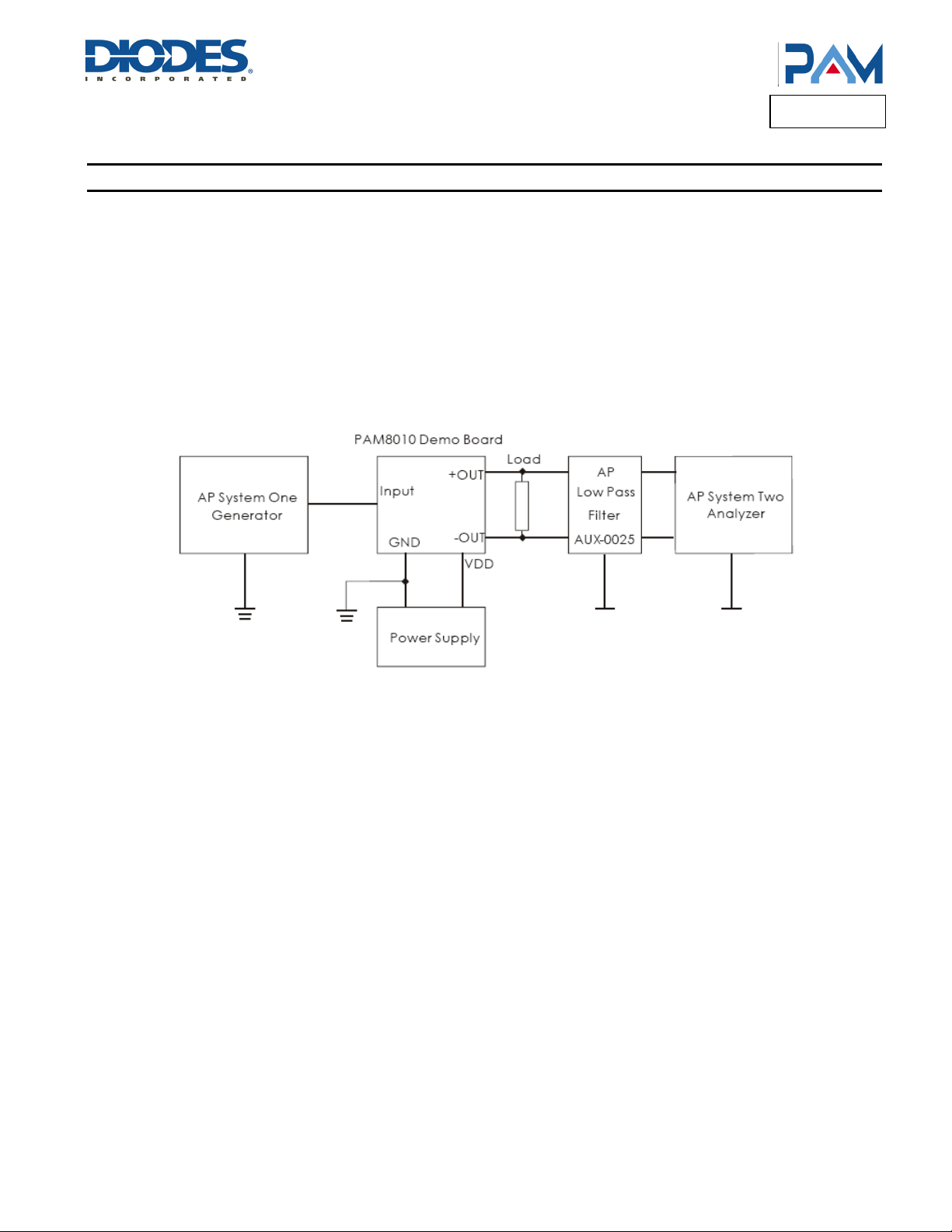
Test Setup for Performance Testing (Class D)
1. When the PAM8010 works with LC filters, it should be connected with the speaker before it's powered on, otherwise it will be damaged easily.
2. When the PAM8010 works without LC filters, it's better to add a ferrite chip bead at the outgoing line of speaker for suppressing the possible
electromagnetic interference.
3. The absolute maximum rating of the PAM8010 operation voltage is 6.0V. When the PAM8010 is powered with four battery cells, it should be
noted that the voltage of four new dry or alkaline batteries is over 6V, higher than its maximum operation voltage, which probably make the
device damaged. Therefore, it's recommended to use either four Ni-MH (Nickel Metal Hydride) rechargeable batteries or three dry or alkaline
batteries.
4. The input signal should not be too high, if too high, it will cause the clipping of output signal when increasing the volume. Because the DC
volume control of the PAM8010 has big gain, it will make the device damaged.
5. When testing the PAM8010 without LC filters by using resistor instead of speaker as the output load, the test results, e.g. THD or efficiency,
will be worse than those using speaker as load.
Notes: 1. The Audio Precision (AP) AUX-0025 low pass filter is necessary for class-D amplifier measurement with AP analyzer.
2. Two 22μH inductors are used in series with load resistor to emulate the small speaker for efficiency measurement.
Power Limit Function
The maximum output power of Class D section is set by applying a DC voltage at PL pin add a resistor divider from AVDD (Pin 6) to ground to
set the voltage at the PL pin. An external reference may alos be used at V
from Pin 7 to ground (see the application circuit on Page 1).
Different from other company’s power limit, the power limit circuit of PAM8010 sets a limit on the output peak voltage, and the value is lower
than the half supply voltage (PV
) makes the PAM8010 never clipping, it means THD+N always lower than 1% when power limit works.
DD
(Pin 7) if tighter tolerance is required. Also add a 1µF capacitor
REF
Noise Reduction Function
The gain of PAM8010 will reduce 12dB when there is no audio at the input of the amplifier for 8s. The gain will recovered until the input signal is
above the noise threshold which is set at V
(Pin 18) and the noise threshold is set by an external resistr from VTH to ground.
TH
Mute Operation
The MUTE_D pin is an input for controlling the Class-D output state of the PAM8010. A logic low on this pin enables the outputs, and a logic
high on this pin disables the outputs. This pin may be used as a quick disable or enable of the outputs without a volume fade. Quiescent current
is listed in the electronics characteristics table. The MUTE_D pin can be left floating due to the internal pull-down.
The MUTE_AB pin is an input for controlling the Class-AB output state of the PAM8010. A logic high on this pin enables the outputs, and a logic
low on this pin disables the outputs.
Shutdown Operation
In order to reduce power consumption while not in use, the PAM8010 contains shutdown circuitry to turn off the amplifier’s bias circuitry. The
amplifier is turned off when logic low is placed on the SHDN pin. By switching the SHDN pin connected to GND, the PAM8010 supply current
draw will be minimized in idle mode. The SHDN pin can be left floating due to the internal pull-up.
For the best power on/off pop performance, the amplifier should be placed in the Mute mode prior to turning on/off the power supply.
PAM8010
Document number: DSxxxxx Rev. 1 - 0
12 of 17
www.diodes.com
November 2012
© Diodes Incorporated
Page 13
A
f
Product Line o
Diodes Incorporated
PAM8010
Application Information
Power Supply Decoupling
The PAM8010 is a high performance CMOS audio amplifier that requires adequate power supply decoupling to ensure the output THD and
PSRR are as low as possible. Power supply decoupling affects low frequency on the power supply leads for higher frey response. Optimum
decoupling is achieved by using two capacitors of different types that target different types of noise frequency transients, spike, or digital hash
on the line, a good low equivalent-series-resisitance (ESR) ceramic capacitor, typically 1.0µF, placed as close as possible to the device V
terminal works best. For filtering lower-frequency noise signals, a large capacitor of 10µF (ceramic) or greater placed near the audio power
amplifier is recommended.
Input Capacitor (CI)
Large input capaciitors are both expensive and spce hungry for portable designs. Clearly, a certain sized capacitor is needed to capacitor is
needed to couple in low frequencies wothout severe attenuation. But in many cases the speakers used in portable systems, whether internal or
external, have little ability to reproduce signals below 100Hz to 150Hz. Thus, using a large input capacitor may not increase actual system
performance. In this case, input capacitor (C
determined equation below,
1
In addition to system cost and size, click and pop perfomance is affected by the size of the input coupling capacitor, CI. A larger inout coupling
capacitor requires more charge to reach its quiescent DC voltage (nominally ½ VDD). This charge comes from the internall circuit via the
feedback and is apt to creat pops upon device enable. Thus, by minimizing the capacitor size based on necessary low frequency response,
turn-on pops can be minimized.
f
C
R2
C
I
I
Analog Refernce Bypass Capacitor (C
Analog Refernce Bypass Capacitor (C
shutdown mode, C
supply caused by coupling into the output drive signal.
determines the rate at which the amplifier starts up. The second function is to reduce noise produced by the power
BYP
BYP
) and input resisitance (RI) of the amplifier form a high-pass filter with the corner frequency
I
)
BYP
) is the most critical capacitor and serves several important functions. During start-up or recovery from
Over Temperature Protection
Thermal protection on the PAM8010 prevents the device from damage when the internal die temperature exceeds +150°C. There is a 15
degree tolerance on this point from device to device. Once the die temperature exceeds the thermal set point, the device outputs are disabled.
This is not a latched fault. The thermal fault is cleared once the temperature of the die is reduced by +40°C. This large hysteresis will prevent
motor boating sound well. The device begins normal operation at this point without external system interaction. Before thermal shutdown, gain
of the PAM8010 will drop -3dB when the chip temperature reaches +120°C.
How to Reduce EMI (Electro Magnetic Interference)
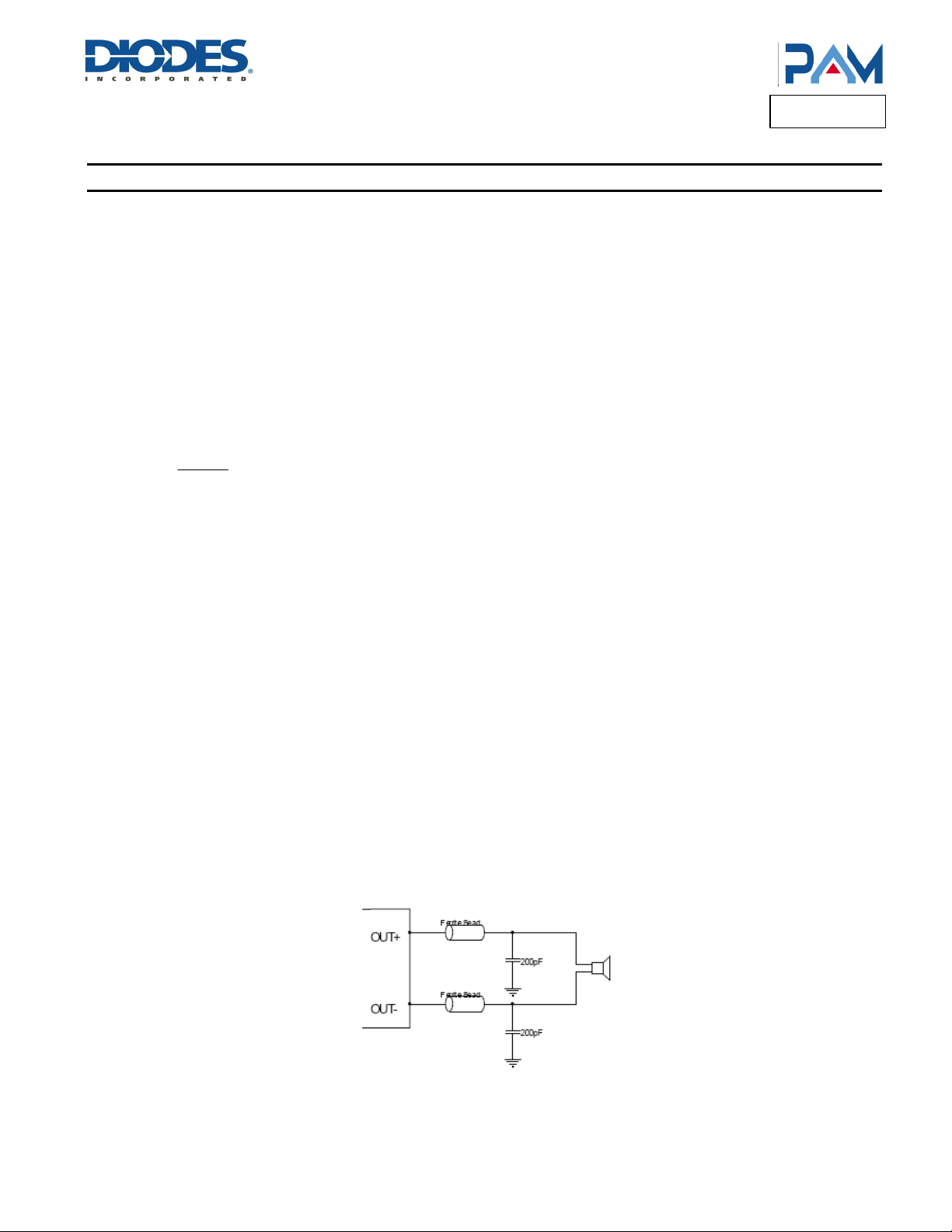
A simple solution is to put an additional capacitor 1000uF at power supply terminal for power line coupling if the traces from amplifier to
speakers are short (< 20CM). Most applications require a ferrite bead filter as shown at Figure 1. The ferrite filter reduces EMI around 1MHz
and higher. When selecting a ferrite bead, choose one with high impedance at high frequencies, and low impedance at low frequencies
(MH2012HM221-T).
DD
Figure 1. Ferrite Bead Filter to Reduce EMI
PAM8010
Document number: DSxxxxx Rev. 1 - 0
13 of 17
www.diodes.com
November 2012
© Diodes Incorporated
Page 14
A
f
Product Line o
Diodes Incorporated
PAM8010
Application Information (cont.)
PCB Layout Guidelines Grounding
At this stage it is paramount to notice the necessity of separate grounds. Noise currents in the output power stage need to be returned to output
noise ground and nowhere else. Were these currents to circulate elsewhere, they may get into the power supply, the signal ground, etc, worse
yet, they may form a loop and radiate noise. Any of these cases results in degraded amplifier performance. The logical returns for the output
noise currents associated with Class-D switching are the respective PGND pins for each channel. The switch state diagram illustrates that
PGND is instrumental in nearly every switch state. This is the perfect point to which the output noise ground trace should return. Also note that
output noise ground is channel specific. A two channel amplifier has two seperate channels and consequently must have two seperate output
noise ground traces. The layout of the PAM8010 offers separate PGND connections for each channel and in some cases each side of the
bridge. Output noise grounds must be tied to system ground at the power in exclusively. Signal currents for the inputs, reference, etc need to be
returned to quite ground. This ground is only tied to the signal components and the GND pin, and GND then tied to system ground.
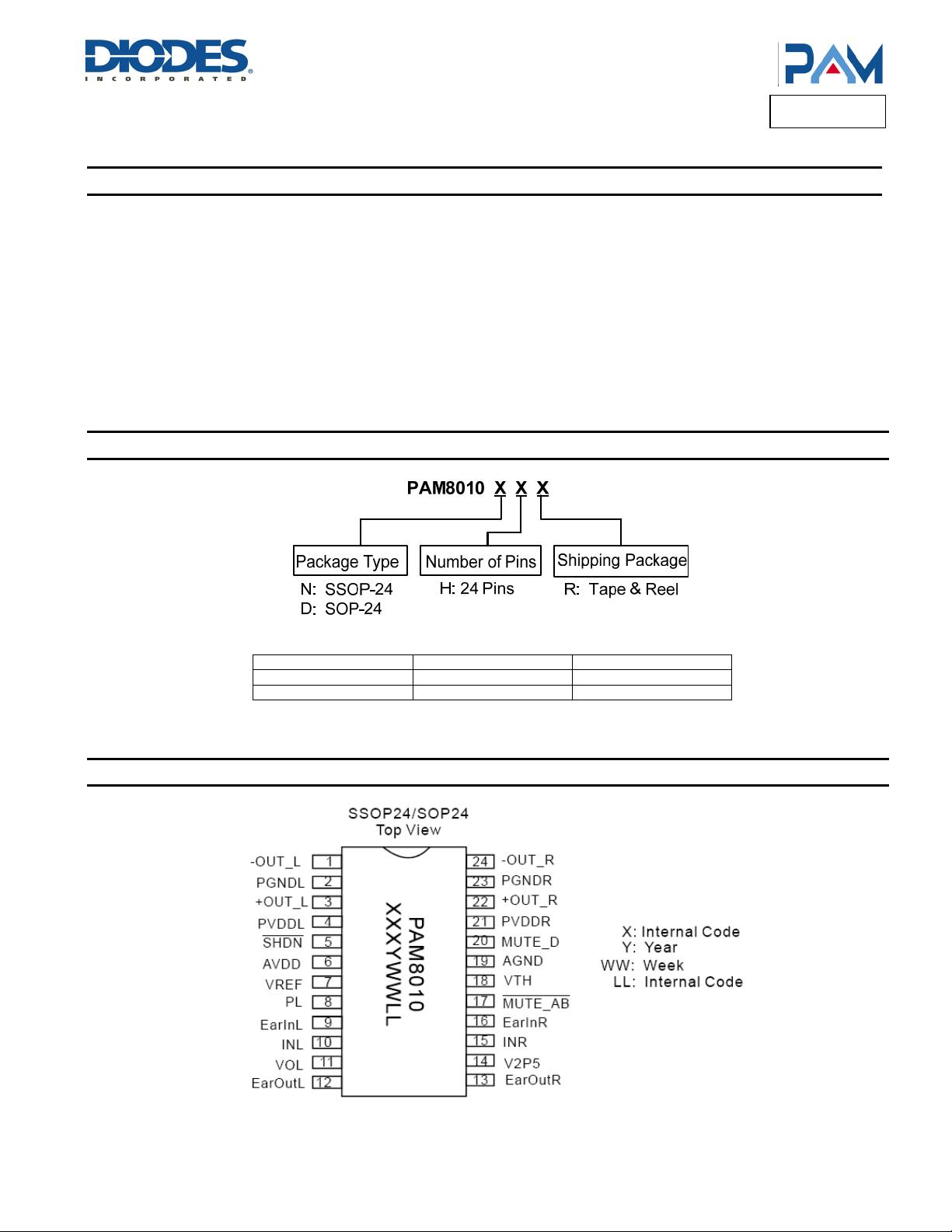
Ordering Information
Marking Information
Part Number Package Type Standard Package
PAM8010NHR SSOP-24 2500 Units/Tape&Reel
PAM8010DHR SOP-24 1000 Units/Tape&Reel
PAM8010
Document number: DSxxxxx Rev. 1 - 0
14 of 17
www.diodes.com
November 2012
© Diodes Incorporated
Page 15
A
f
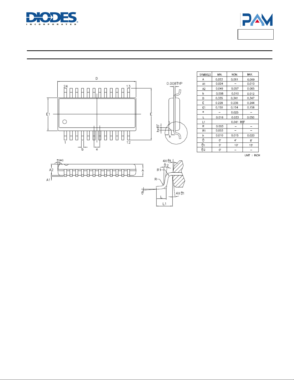
Package Outline Dimensions (All dimensions in mm.)
SSOP-24
Product Line o
Diodes Incorporated
PAM8010
PAM8010
Document number: DSxxxxx Rev. 1 - 0
15 of 17
www.diodes.com
November 2012
© Diodes Incorporated
Page 16
A
f
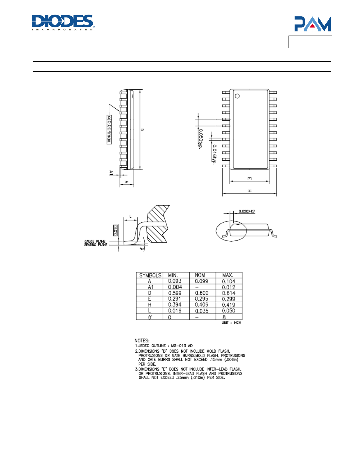
Package Outline Dimensions (cont.) (All dimensions in mm.)
SOP-24
Product Line o
Diodes Incorporated
PAM8010
PAM8010
Document number: DSxxxxx Rev. 1 - 0
16 of 17
www.diodes.com
November 2012
© Diodes Incorporated
Page 17

A
f
Product Line o
Diodes Incorporated
PAM8010
DIODES INCORPORATED MAKES NO WARRANTY OF ANY KIND, EXPRESS OR IMPLIED, WITH REGARDS TO THIS DOCUMENT,
INCLUDING, BUT NOT LIMITED TO, THE IMPLIED WARRANTIES OF MERCHANTABILITY AND FITNESS FOR A PARTICULAR PURPOSE
(AND THEIR EQUIVALENTS UNDER THE LAWS OF ANY JURISDICTION).
Diodes Incorporated and its subsidiaries reserve the right to make modifications, enhancements, improvements, corrections or other changes
without further notice to this document and any product described herein. Diodes Incorporated does not assume any liability arising out of the
application or use of this document or any product described herein; neither does Diodes Incorporated convey any license under its patent or
trademark rights, nor the rights of others. Any Customer or user of this document or products described herein in such applications shall assume
all risks of such use and will agree to hold Diodes Incorporated and all the companies whose products are represented on Diodes Incorporated
website, harmless against all damages.
Diodes Incorporated does not warrant or accept any liability whatsoever in respect of any products purchased through unauthorized sales channel.
Should Customers purchase or use Diodes Incorporated products for any unintended or unauthorized application, Customers shall indemnify and
hold Diodes Incorporated and its representatives harmless against all claims, damages, expenses, and attorney fees arising out of, directly or
indirectly, any claim of personal injury or death associated with such unintended or unauthorized application.
Products described herein may be covered by one or more United States, international or foreign patents pending. Product names and markings
noted herein may also be covered by one or more United States, international or foreign trademarks.
This document is written in English but may be translated into multiple languages for reference. Only the English version of this document is the
final and determinative format released by Diodes Incorporated.
Diodes Incorporated products are specifically not authorized for use as critical components in life support devices or systems without the express
written approval of the Chief Executive Officer of Diodes Incorporated. As used herein:
A. Life support devices or systems are devices or systems which:
1. are intended to implant into the body, or
2. support or sustain life and whose failure to perform when properly used in accordance with instructions for use provided in the
labeling can be reasonably expected to result in significant injury to the user.
B. A critical component is any component in a life support device or system whose failure to perform can be reasonably expected to cause the
failure of the life support device or to affect its safety or effectiveness.
Customers represent that they have all necessary expertise in the safety and regulatory ramifications of their life support devices or systems, and
acknowledge and agree that they are solely responsible for all legal, regulatory and safety-related requirements concerning their products and any
use of Diodes Incorporated products in such safety-critical, life support devices or systems, notwithstanding any devices- or systems-related
information or support that may be provided by Diodes Incorporated. Further, Customers must fully indemnify Diodes Incorporated and its
representatives against any damages arising out of the use of Diodes Incorporated products in such safety-critical, life support devices or systems.
Copyright © 2012, Diodes Incorporated
www.diodes.com
IMPORTANT NOTICE
LIFE SUPPORT
PAM8010
Document number: DSxxxxx Rev. 1 - 0
17 of 17
www.diodes.com
November 2012
© Diodes Incorporated
 Loading...