

Page 1
A
f
300mA HIGH PSRR LOW-DROPOUT CMOS LINEAR REGULATOR
Description
The PAM3101 series of positive voltage linear regulators feature low
quiescent current (65µA typ.) and low dropout voltage, making them
ideal for battery powered applications. Their high PSRR make them
useful in applications where AC noise on the input power supply must
be suppressed. Space-saving TSOT25, SOT-23, SOT-89, SC70 and
DFN1.6x1.6-6L packages are attractive for portable and handheld
applications. They have both thermal shutdown and current limit
features to prevernt device failure from extreme operating conditions.
They are stable with an output capacitor of 2.2µF or greater.
Features
Low Dropout Voltage: 180mV@300mA (VO = 3.3V)
Output Voltage Accuracy within ±2%
Supply Voltage Range: 2.5V to 5.5V
Quiescent Current: 65µA typ.
High PSRR: 70dB@1kHz
Excellent Line and Regulation
Fast Discharge
Current Limiting
Short Circuit Protection
Low Temperature Coefficient
Shutdown Current: 0.5µA
Thermal Shutdown
Space Saving Packages: TSOT25, SOT-23, SOT-89, SC70 and
DFN1.6x1.6
Pb-Free Packages
Applications
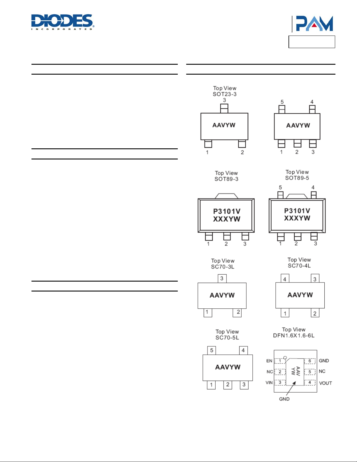
Pin Assignments
Product Line o
Diodes Incorporated
PAM3101
Top View
TSOT25
Cellular Phones
Bluetooth Earphones
Digital Cameras
Portable Electronics
WLANs
MP3 Players
PAM3101
Document number: DSxxxxx Rev. 2 - 5
1 of 25
www.diodes.com
October 2012
© Diodes Incorporated
Page 2
A
f
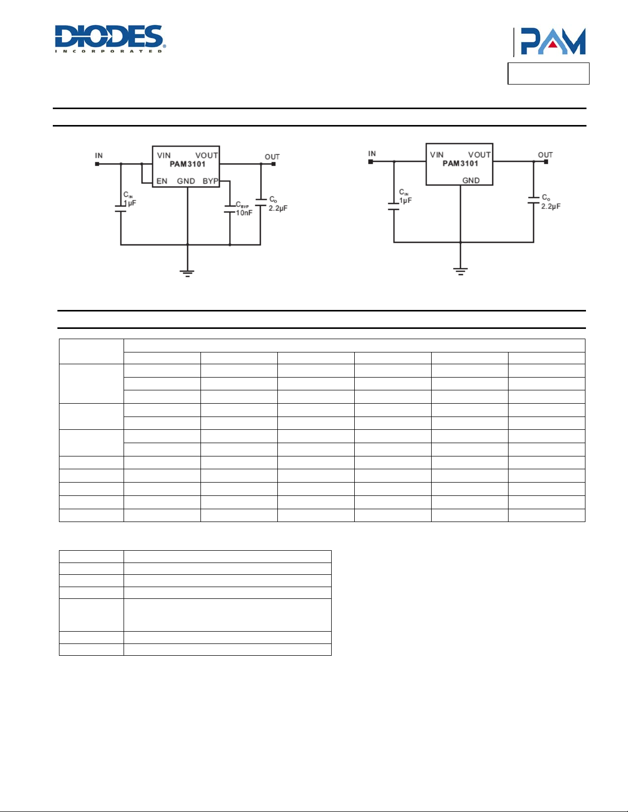
Typical Applications Circuit
Product Line o
Diodes Incorporated
PAM3101
Pin Configuration and Description
Package
Type
SOT23-3
TSOT25
SOT89-3
SOT89-5
SC-70-3L
SC70-4L
SC70-5L
DFN1.6x1.6-6L
Pin Name Function
VIN Input
GND Ground
VOUT Output
EN
BYP Bypass Pin, need a 10nF capacitor connect to GND
NC No Connection
1 2 3 4 5 6
GND
VIN
VOUT
VIN
VIN
GND
VOUT
VOUT
VIN
EN
VIN
EN
Chip Enable (active high)
PAM3101BABXXX----EN default floating
Other part no----EN default pull high
VOUT VIN — — —
VOUT GND — — —
GND VIN — — —
GND EN BYP VOUT —
GND EN NC VOUT —
VIN VOUT — — —
GND VIN — — —
GND NC EN VIN —
VOUT GND — — —
GND VOUT VIN — —
GND EN BYP VOUT —
NC VIN VOUT NC GND
Pin Number
PAM3101
Document number: DSxxxxx Rev. 2 - 5
2 of 25
www.diodes.com
October 2012
© Diodes Incorporated
Page 3
A
f
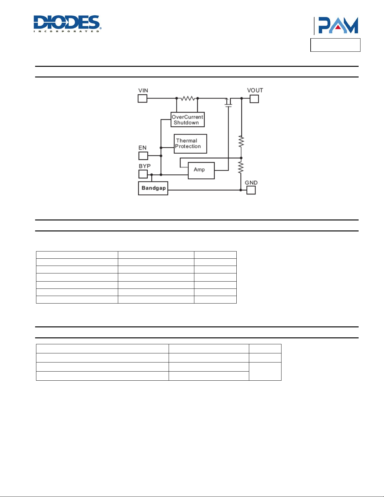
Functional Block Diagram
Product Line o
Diodes Incorporated
PAM3101
Absolute Maximum Ratings (@T
These are stress ratings only and functional operation is not implied. Exposure to absolute maximum ratings for prolonged time periods may
affect device reliability. All voltages are with respect to ground.
Parameter Rating Unit
Input Voltage 6.0 V
Output Current 300 mA
Output Pin Voltage
Lead Soldering Temperature 300, (5sec) °C
Storage Temperature -65 to +150 °C
ESD Rating Class B
= +25°C, unless otherwise specified.)
A
GND -0.3 to V
+0.3V
IN
Recommended Operating Conditions (@T
Parameter Rating Unit
Supply Voltage Range 2.5 to 5.5 V
Junction Temperature -40 to +125
Operation Temperature -40 to +85
PAM3101
Document number: DSxxxxx Rev. 2 - 5
www.diodes.com
V
= +25°C, unless otherwise specified.)
A
3 of 25
°C
October 2012
© Diodes Incorporated
Page 4
A
f
Product Line o
Diodes Incorporated
PAM3101
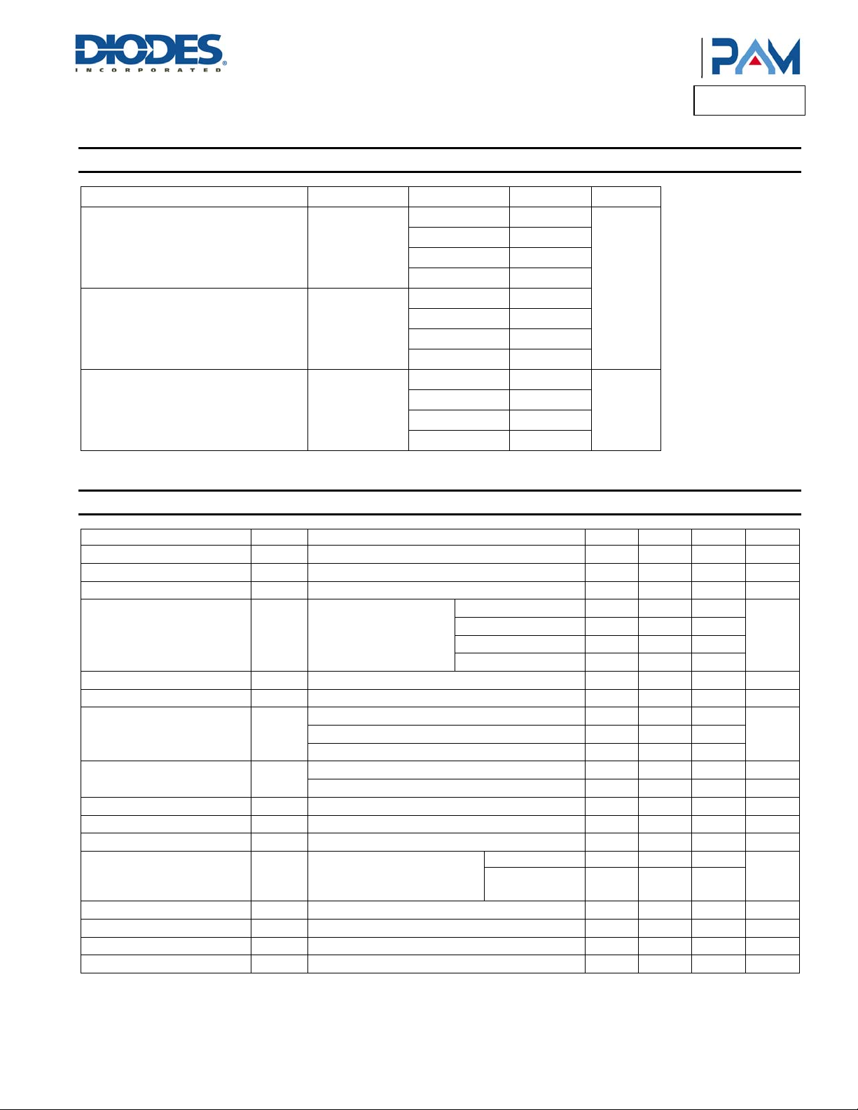
Thermal Information
Parameter Symbol Package Max Unit
TSOT25/SOT23 130
Thermal Resistance Junction to Case)
Thermal Resistance (Junction to Ambient)
θ
JC
θ
JA
Internal Power Dissipation (@TA = 25°C) PD
Electrical Characteristics (@T
= +25°C, V
A
CE1
= V
Parameter Symbol Test Conditions Min Typ Max Units
Input Voltage
Output Voltage
V
V
Output Current
Dropout Voltage
Ground Current
V
I
DROP
GND
Quiescent Current
Line Regulation LNR
IN
IO = 1mA
O
300 Note 2 mA
I
O
IO = 300mA
IO = 1mA to 300mA
I
IO = 0mA
Q
I
= 1mA, VO < 2V, VIN = 2.8V to 3.8V
O
IO = 1mA, 2V ≤ VO < 3.3V, VIN = VO +0.5V to VO +1V
IO = 1mA, VO ≥ 3.3V, VIN = VO +0.5V to VO +1V
I
= 1mA to 300mA, VO ≥ 2V
Load Regulation LDR
Temperature Coefficient
T
Over Temperature Shutdown OTS
Over Temperature Hysteresis OTH
Power Supply Ripple Rejection PSRR
Output Noise
CE Input High Threshold
CE Input Low Threshold
Shutdown Current
Notes: 1. The minimym inout voltage (V
V
2. Output current is limited by P
IN(MIN)
= VO +V
DROP
V
V
V
I
SD
IN(MIN
, maximum IO = PD/(V
D
O
IO = 1mA to 300mA, VO < 2V
IO = 1mA
C
I
= 1mA
O
I
= 1mA
O
= 100mA
I
O
C
= 10nF
BYP
= 3.3V
V
O
f = 10Hz to 100kHz, C
N
VIN = 2.5V to 5V
TH
VIN = 2.5V to 5V
TL
VEN = 0V
) of the PAM3101 is determined by output voltage and dropout voltage. The minimum input voltage is defined as:
IN(MAX)
PAM3101
Document number: DSxxxxx Rev. 2 - 5
SOT-89 100
SC70 160
DFN1.6x1.6 65
TSOT25/SOT23 250
°C/W
SOT-89 180
SC70 300
DFN1.6x1.6 175
TSOT25/SOT23 400
SOT-89 550
SC70 300
mW
DFN1.6x1.6 570
= VIN = VO +1V, CIN = 2.2µF, CO = 2.2µF, unless otherwise specified.)
CE2
Note 1 5.5 V
-2 +2 %
= 1.5V
V
O
VO = 1.8V
2.5V ≤ VO < 3.3V
VO ≥ 3.3V
1150 1400
850 1100
370 450
180 230
70 90 µA
65 90 µA
-0.15 0.10 0.15
-0.10 0.03 0.10
-0.4 0.2 0.4
-2 1 +2 %
30 60 mV
40 ppm/°C
150 °C
30 °C
f = 100Hz 70
f = 1kHz 65
BYP
= 10nF
50
1.5 V
0.3 V
0.01 1 µA
– VO).
4 of 25
www.diodes.com
mV
%/V
dB
µV
RMS
October 2012
© Diodes Incorporated
Page 5
A
f
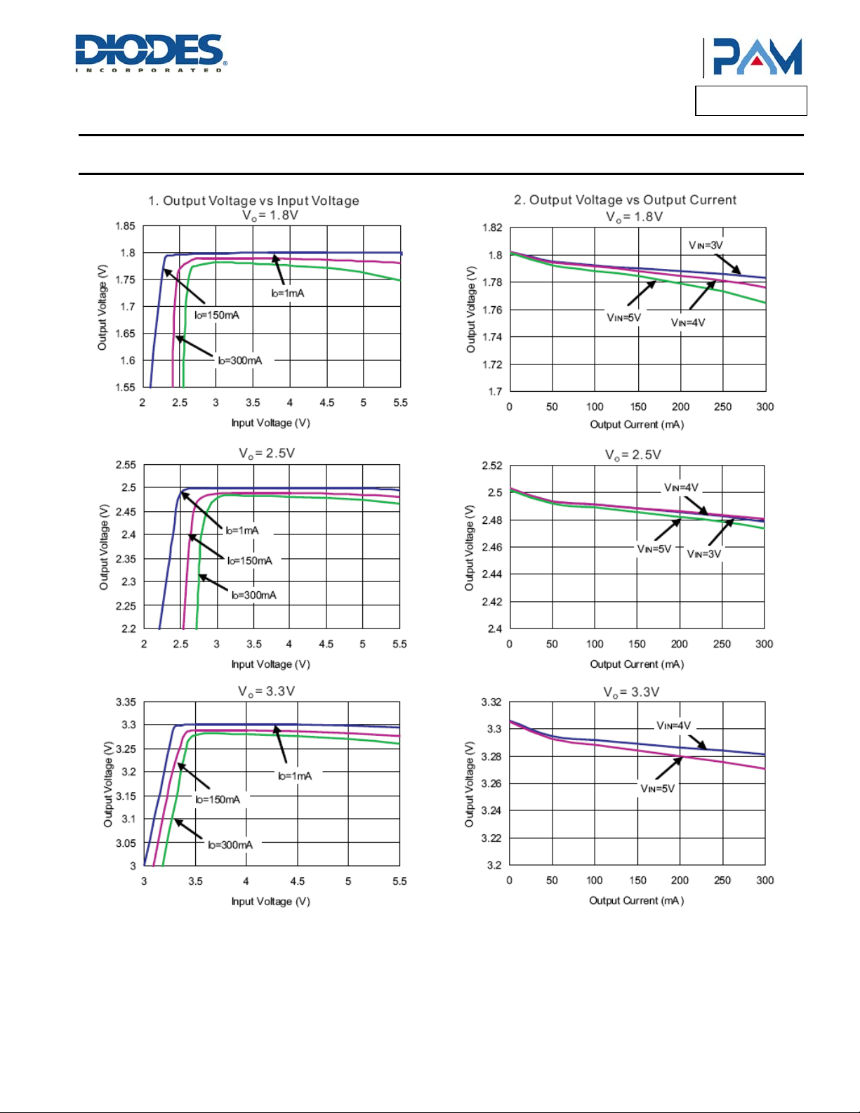
Typical Performance Characteristics
(@TA = +25°C, VEN = VIN, CIN = 1µF, CO = 2.2µF, C
= 10nF unless otherwise specified.)
BYP
Product Line o
Diodes Incorporated
PAM3101
PAM3101
Document number: DSxxxxx Rev. 2 - 5
www.diodes.com
5 of 25
October 2012
© Diodes Incorporated
Page 6
A
f
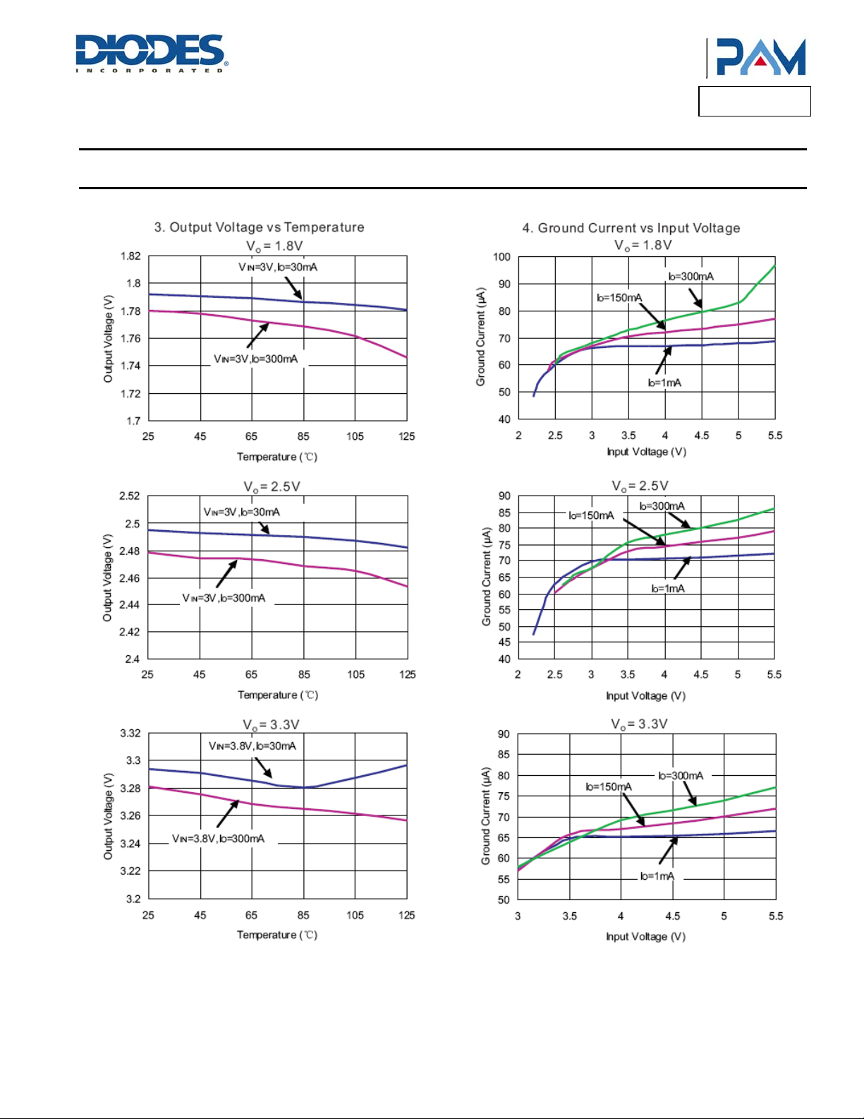
Typical Performance Characteristics (cont.)
(@TA = +25°C, VEN = VIN, CIN = 1µF, CO = 2.2µF, C
= 10nF unless otherwise specified.)
BYP
Product Line o
Diodes Incorporated
PAM3101
PAM3101
Document number: DSxxxxx Rev. 2 - 5
6 of 25
www.diodes.com
October 2012
© Diodes Incorporated
Page 7
A
f
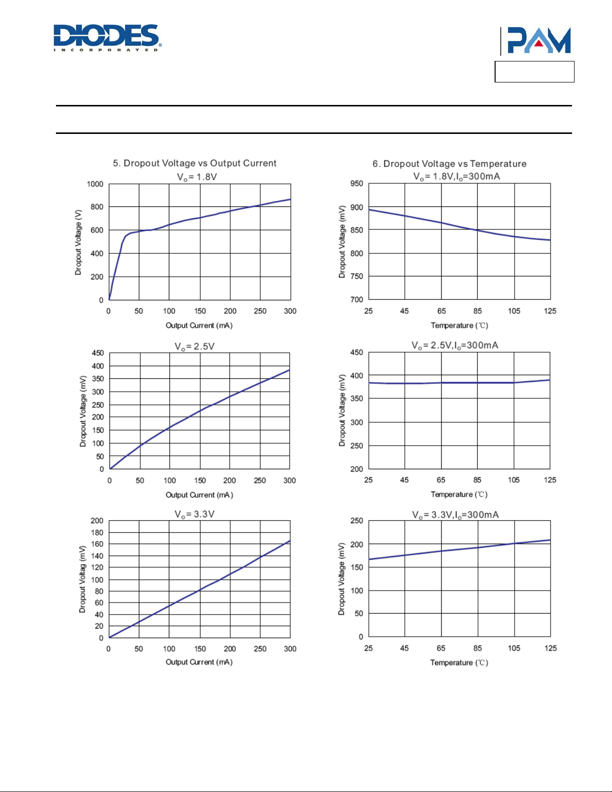
Typical Performance Characteristics (cont.)
(@TA = +25°C, VEN = VIN, CIN = 1µF, CO = 2.2µF, C
= 10nF unless otherwise specified.)
BYP
Product Line o
Diodes Incorporated
PAM3101
PAM3101
Document number: DSxxxxx Rev. 2 - 5
www.diodes.com
7 of 25
October 2012
© Diodes Incorporated
Page 8
A
f
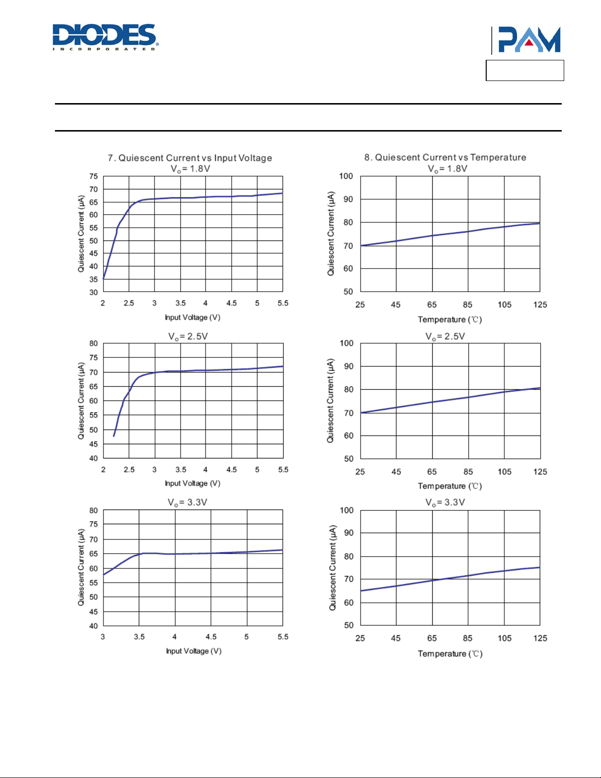
Typical Performance Characteristics (cont.)
(@TA = +25°C, VEN = VIN, CIN = 1µF, CO = 2.2µF, C
= 10nF unless otherwise specified.)
BYP
Product Line o
Diodes Incorporated
PAM3101
PAM3101
Document number: DSxxxxx Rev. 2 - 5
8 of 25
www.diodes.com
October 2012
© Diodes Incorporated
Page 9

A
f
Typical Performance Characteristics (cont.)
(@TA = +25°C, VEN = VIN, CIN = 1µF, CO = 2.2µF, C
= 10nF unless otherwise specified.)
BYP
Product Line o
Diodes Incorporated
PAM3101
PAM3101
Document number: DSxxxxx Rev. 2 - 5
9 of 25
www.diodes.com
October 2012
© Diodes Incorporated
Page 10

A
f
Typical Performance Characteristics (cont.)
(@TA = +25°C, VEN = VIN, CIN = 1µF, CO = 2.2µF, C
= 10nF unless otherwise specified.)
BYP
Product Line o
Diodes Incorporated
PAM3101
PAM3101
Document number: DSxxxxx Rev. 2 - 5
www.diodes.com
10 of 25
October 2012
© Diodes Incorporated
Page 11

A
f
Product Line o
Diodes Incorporated
PAM3101
Application Information
Capacitor Selection and Regulator Stability
Similar to any low dropout regulator, the external capacitors used with the PAM3101 must be carefully selected for regulator stability and
performance.
A capacitor C
distance between C
Capacitors with larger values and lower ESR (equivalent series resistance) provide better PSRR and line-transient response.
The PAM3101 is designed specifically to work with low ESR ceramic output capacitors in order to save space and improve performance. Using
an output ceramic capacitor whose value is >2.2μF with ESR>5mΩ ensures stability.
A 10nF bypass capacitor connected to BYP pin is suggested for suppressing output noise. The capacitor, in series connection with an internal
200kΩ resistor, forms a low-pass filter for noise reduction. Increasing the capacitance will slightly decrease the output noise, but increase the
start-up time.
Load Transient Consideration
Curve 10 of the PAM3101 load-transient response on page 10 shows two components of the output response: a DC shift from the output
impedance due to the load current change and transient response. The DC shift is quite small due to excellent load regulation of the PAM3101.
The transient spike, resulting from a step change in the load current from 1mA to 300mA, is 20mV. The ESR of the output capacitor is critical to
the transient spike. A larger capacitance with smaller ESR results in a smaller spike.
Shutdown Input Operation
The PAM3101 is shut down by pulling the EN input low, and is turned on by tying the EN input to VIN.
Internal P-Channel Pass Transistor
The PAM3101 features a 0.75Ω P-Channel MOSFET device as a pass transistor. The PMOS pass transistor enables the PAM3101 to consume
only 65μA of ground current during low dropout, light-load, or heavy-load operations. This feature increases the battery operation life time.
Input-Output (Dropout) Voltage
A regulator's minimum input-output voltage difference (or dropout voltage) determines the lowest usable supply voltage. The PAM3101 has a
typical 300mV dropout voltage. In battery powered systems, this will determine the useful end-of-life battery voltage.
Current Limit and Short Circuit Protection
The PAM3101 features a current limit, which monitors and controls the gate voltage of the pass transistor. The output current can be limited to
400mA by regulating the gate voltage. The PAM3101 also has a built-in short circuit current limit.
Thermal Considerations
Thermal protection limits power dissipation in the PAM3101. When the junction temperature exceeds +150°C, the OTP (Over Temperature
Protection) starts the thermal shutdown and turns the pass transistor off. The pass transistor resumes operation after the junction temperature
drops below +120°C.
For continuous operation, the junction temperature should be maintained below +125°C. The power dissipation is defined as:
of more than 1μF can be employed in the input pin, while there is no upper limit for the capacitance of CIN. Please note that the
IN
and the input pin of the PAM3101 should not exceed 0.5 inch. Ceramic capacitors are suitable for the PAM3101.
IN
VVP
*
VI
*
I
GNDINOOUTIND
The maximum power dissipation depends on the thermal resistance of IC package, PCB layout, the rate of surrounding airflow and temperature
difference between junction and ambient. The maximum power dissipation can be calculated by the following formula:
Where T
junction to the ambient.
is the maximum allowable junction temperature +125°C , TA is the ambient temperature and θJA is the thermal resistance from the
J(MAX)
PAM3101
Document number: DSxxxxx Rev. 2 - 5
/
TTP
A)MAX(J)MAX(D
JA
11 of 25
www.diodes.com
October 2012
© Diodes Incorporated
Page 12

A
f
Application Information
For example, as θ
layer thermal test board, the maximum power dissipation at T
P
P
is 250°C/W for the SOT-23 package and 180°C/W for the SOT-89 package based on the standard JEDEC 51-3 f or a single-
JA
)MAX(D
)MAX(D
(cont.)
SOT-23
SOT-89
W4.0250/C25C125
W55.0180/C25C125
Product Line o
Diodes Incorporated
+25°C can be calculated by following formula:
A
PAM3101
It is also useful to calculate the junction temperature of the PAM3101 under a set of specific conditions. Suppose the input voltage V
the output current I
= 2.8V version of the PAM3101 can be calculated as:
the V
O
And the junction temperature, T
T
T
= 40°C +37.5°C
= 77.5°C<T
For this application, T
configuration.
P
D
J
J
= 300mA and the case temperature TA = +40°C measured by a thermalcouple during operation, the power dissipation for
O
can be calculated as follows:
J
= TA + PD*θJA
= 40°C +0.15W*250°C/W
= +125°C
J(MAX)
is lower than the absolute maximum operating junction temperature, +125°C, so it is safe to use the PAM3101 in this
J
mW150A70*V3.3mA300*V8.2V3.3
= 3.3V,
IN
PAM3101
Document number: DSxxxxx Rev. 2 - 5
12 of 25
www.diodes.com
October 2012
© Diodes Incorporated
Page 13

A
f
Ordering Information
Product Line o
Diodes Incorporated
PAM3101
Pin Configuration Package Type Number of Pins Output Voltage
A Type:
1. GND
2. VOUT
3. VIN
B Type:
1. VIN
2. GND
3. EN
(EN Default
floating
4. NC
5. VOUT
C Type:
1. VOUT
2. GND
3. VIN
D Type:
1. VIN
2.GND
3.EN
(EN Default
pull high
4.BYP
5.VOUT
E Type:
F Type:
G Type:
H Type:
1. VOUT
2. GND
3. NC
4. EN
(EN Default
floating
5. VIN
1. EN
(EN Default
floating
2. NC
3. VIN
4. VOUT
5. NC
6. GND
1. VIN
2. VOUT
3. GND
1. GND
2. VIN
A: TSOT25/SOT23
C: SOT-89
U: SC70
K: DFN1.6x1.6
A: 3
K: 4
B: 5
F: 6
475: 4.75V
400: 4.0V
380: 3.8V
330: 3.3 V
310: 3.1V
290: 2.9V
285: 2.85V
280: 2.8V
250: 2.5V
200: 2.0V
180: 1.8V
150: 1.5V
3. VOUT
PAM3101
Document number: DSxxxxx Rev. 2 - 5
13 of 25
www.diodes.com
October 2012
© Diodes Incorporated
Page 14

A
f
Ordering Information (cont.)
Product Line o
Diodes Incorporated
PAM3101
PAM3101
Document number: DSxxxxx Rev. 2 - 5
14 of 25
www.diodes.com
© Diodes Incorporated
October 2012
Page 15

A
f
Ordering Information (cont.)
Product Line o
Diodes Incorporated
PAM3101
PAM3101
Document number: DSxxxxx Rev. 2 - 5
15 of 25
www.diodes.com
© Diodes Incorporated
October 2012
Page 16

A
f
Ordering Information (cont.)
Product Line o
Diodes Incorporated
PAM3101
PAM3101
Document number: DSxxxxx Rev. 2 - 5
16 of 25
www.diodes.com
© Diodes Incorporated
October 2012
Page 17

A
f
Ordering Information (cont.)
Product Line o
Diodes Incorporated
PAM3101
PAM3101
Document number: DSxxxxx Rev. 2 - 5
www.diodes.com
17 of 25
© Diodes Incorporated
October 2012
Page 18

A
f
Marking Information
Top View
TSOT25
Product Line o
Diodes Incorporated
PAM3101
PAM3101
Document number: DSxxxxx Rev. 2 - 5
18 of 25
www.diodes.com
October 2012
© Diodes Incorporated
Page 19

A
f
Package Outline Dimensions (All dimensions in mm.)
SOT23-3
Product Line o
Diodes Incorporated
PAM3101
PAM3101
Document number: DSxxxxx Rev. 2 - 5
19 of 25
www.diodes.com
October 2012
© Diodes Incorporated
Page 20

A
f
Package Outline Dimensions (cont.) (All dimensions in mm.)
TSOT25
Product Line o
Diodes Incorporated
PAM3101
PAM3101
Document number: DSxxxxx Rev. 2 - 5
20 of 25
www.diodes.com
© Diodes Incorporated
October 2012
Page 21

A
f
Package Outline Dimensions (cont.) (All dimensions in mm.)
Product Line o
Diodes Incorporated
PAM3101
PAM3101
Document number: DSxxxxx Rev. 2 - 5
21 of 25
www.diodes.com
October 2012
© Diodes Incorporated
Page 22

A
f
Package Outline Dimensions (cont.) (All dimensions in mm.)
Product Line o
Diodes Incorporated
PAM3101
PAM3101
Document number: DSxxxxx Rev. 2 - 5
22 of 25
www.diodes.com
October 2012
© Diodes Incorporated
Page 23

A
f
Package Outline Dimensions (All dimensions in mm.)
Product Line o
Diodes Incorporated
PAM3101
PAM3101
Document number: DSxxxxx Rev. 2 - 5
23 of 25
www.diodes.com
October 2012
© Diodes Incorporated
Page 24

A
f
Package Outline Dimensions (All dimensions in mm.)
DFN 1.6x1.6-6L
Product Line o
Diodes Incorporated
PAM3101
PAM3101
Document number: DSxxxxx Rev. 2 - 5
www.diodes.com
24 of 25
October 2012
© Diodes Incorporated
Page 25

A
f
Product Line o
Diodes Incorporated
PAM3101
DIODES INCORPORATED MAKES NO WARRANTY OF ANY KIND, EXPRESS OR IMPLIED, WITH REGARDS TO THIS DOCUMENT,
INCLUDING, BUT NOT LIMITED TO, THE IMPLIED WARRANTIES OF MERCHANTABILITY AND FITNESS FOR A PARTICULAR PURPOSE
(AND THEIR EQUIVALENTS UNDER THE LAWS OF ANY JURISDICTION).
Diodes Incorporated and its subsidiaries reserve the right to make modifications, enhancements, improvements, corrections or other changes
without further notice to this document and any product described herein. Diodes Incorporated does not assume any liability arising out of the
application or use of this document or any product described herein; neither does Diodes Incorporated convey any license under its patent or
trademark rights, nor the rights of others. Any Customer or user of this document or products described herein in such applications shall assume
all risks of such use and will agree to hold Diodes Incorporated and all the companies whose products are represented on Diodes Incorporated
website, harmless against all damages.
Diodes Incorporated does not warrant or accept any liability whatsoever in respect of any products purchased through unauthorized sales channel.
Should Customers purchase or use Diodes Incorporated products for any unintended or unauthorize d application, Customers shall indemnify and
hold Diodes Incorporated and its representatives harmless against all claims, damages, expenses, and attorney fees arising out of, directly or
indirectly, any claim of personal injury or death associated with such unintended or unauthorized application.
Products described herein may be covered by one or more United States, international or foreign patents pending. Product names and markings
noted herein may also be covered by one or more United States, international or foreign trademarks.
This document is written in English but may be translated into multiple languages for reference. Onl y the English version of this document is the
final and determinative format released by Diodes Incorporated.
Diodes Incorporated products are specifically not authorized for use as critical components in life support devices or systems without the express
written approval of the Chief Executive Officer of Diodes Incorporated. As used herein:
A. Life support devices or systems are devices or systems which:
1. are intended to implant into the body, or
2. support or sustain life and whose failure to perform when properly used in accordance with instructions for use provided in the
labeling can be reasonably expected to result in significant injury to the user.
B. A critical component is any component in a life support device or system whose failure to perform can be reasonably expected to cause the
failure of the life support device or to affect its safety or effectiveness.
Customers represent that they have all necessary expertise in the safety and regulatory ramifications of their life support devices or systems, and
acknowledge and agree that they are solely responsible for all legal, regulatory and safety-related requirements concerning their products and any
use of Diodes Incorporated products in such safety-critical, life support devices or systems, notwithstanding any devices- or systems-related
information or support that may be provided by Diodes Incorporated. Further, Customers must fully indemnify Diodes Incorporated and its
representatives against any damages arising out of the use of Diodes Incorporated products in such safety-critical, life support devices or systems.
Copyright © 2013, Diodes Incorporated
www.diodes.com
IMPORTANT NOTICE
LIFE SUPPORT
PAM3101
Document number: DSxxxxx Rev. 2 - 5
25 of 25
www.diodes.com
October 2012
© Diodes Incorporated
 Loading...