

Page 1
A
f
Product Line o
Diodes Incorporated
PAM2845
40V HIGH POWER BOOST CONVERTER with
6 CHANNEL CONSTANT CURRENT SOURCE
Description
The PAM2845 is a high-efficiency boost type LED driver. It is
designed for large LCD panel that employs an array of LEDs as back
light source.
The PAM2845 employs a current-mode step-up converter that drives
six parallel strings of LEDs connected in multiple series. This built-in
string current-control circuit achieves ±1% typical current matching
between strings, which ensures even brightness for all LEDs.
Separate feedback loops limit the output voltage if one or more LEDs
open or short. The PAM2845 has features cycle-by-cycle current limit
to provide consistent operation and soft-start capability. A thermal-
shutdown circuit provides another level of protection.
The PAM2845 has a wide +4.8V to +28V input voltage range and
provides adjustable full-scale LED current. The switching frequency of
this device can be selected among 500kHz, 1MHz and 1.6MHz
according to the application requirements.
Features
• Six Constant-Current Output Channels
• Parallel Channels Allow Higher Current per LED String
• Maximum 40V Continuous Voltage Output Limit for Each
Channel
• Adjustable Constant Output Voltage
• Adjustable Constant LED Current
• Drives 10 or more LEDs Each String as Long as the String
Voltage Less Than 40V
• Internal 2.5A Power MOSFET
• Allows Digital PWM and Analog Dimming
• Wide (100:1) PWM Dimming Range without Color Shift
• Independent Dimming and Shutdown Control of the LED Driver
• ±1% Typical Current Matching between Strings
• Short LED Protection
• 3 Frequencies Selection: 1.6MHz/1MHz/500kHz
• Wide Input Voltage Range: 4.8V to 28V
• Over Temperature Protection
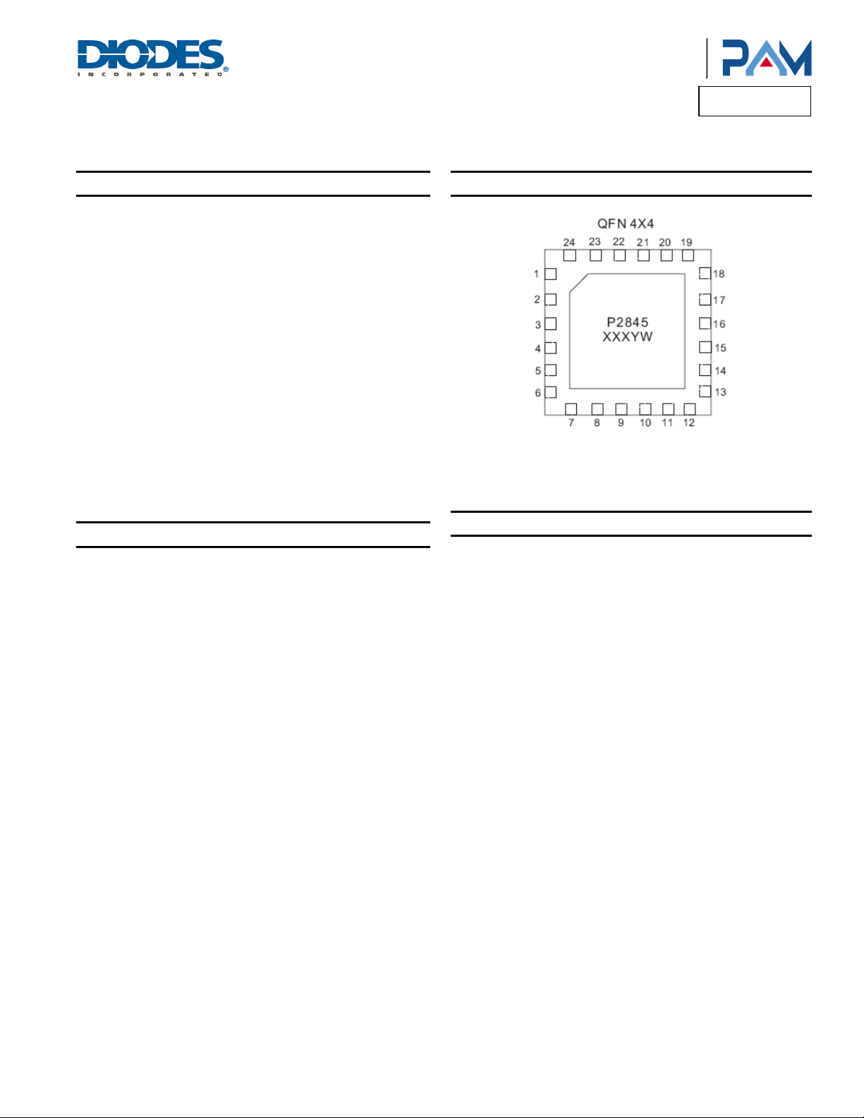
• Available in 24-pin 4mmx4mm QFN Package
• Pb-free Package
Pin Assignments
Applications
• White or RGB Backlighting for LCD, TV, LCD Monitor, Notebook,
Handy Terminals, and Avionics Displays Panels
• LED Lighting Devices
PAM2845
Document number: DSxxxxx Rev. 1 - 2
1 of 14
www.diodes.com
October 2012
© Diodes Incorporated
Page 2
A
f
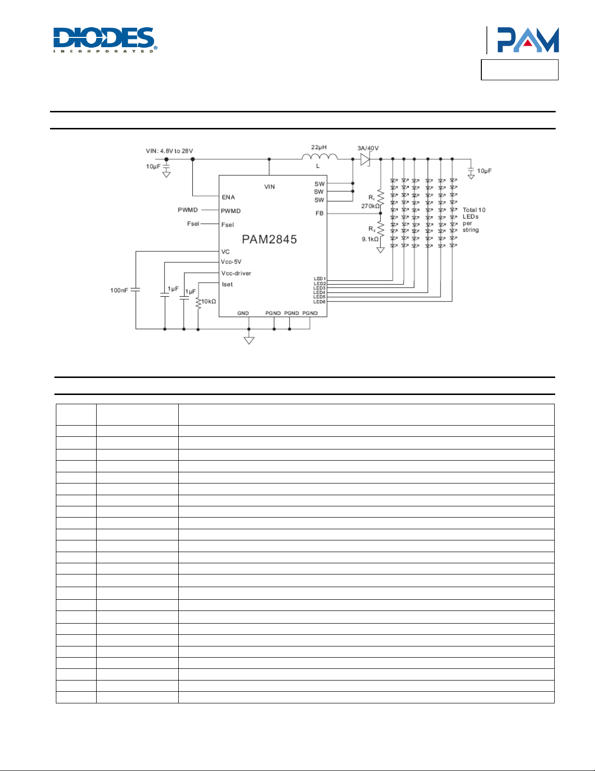
Typical Applications Circuit
Product Line o
Diodes Incorporated
PAM2845
Pin Descriptions
Pin
Number
1 VIN Supply Input
2
3 GND Ground
4 ENA Enable Input
5 PWMD PWM Dimming Control
6 LED1 LED1 Cathode Terminal
7 LED2 LED2 Cathode Terminal
8 LED3 LED3 Cathode Terminal
9 GND Ground
10 GND Ground
11 LED4 LED4 Cathode Terminal
12 LED5 LED5 Cathode Terminal
13 LED6 LED6 Cathode Terminal
14
15
16 VC Boost Stage Compensation Pin
17
18 FB Feedback
19 PGND Power Ground
20 PGND Power Ground
21 PGND Power Ground
22 SW Power MOS Drain
23 SW Power MOS Drain
24 SW Power MOS Drain
Pin Name
QFN4x4-24
V
-Driver
CC
I
SET
V
-5V
CC
F
SEL
5V Linear Regulator Output for Power MOS Driver
LED Current Adjustment Pin
5V Linear Regulator
Oscillator Frequency Selection Pin
Function
PAM2845
Document number: DSxxxxx Rev. 1 - 2
2 of 14
www.diodes.com
October 2012
© Diodes Incorporated
Page 3
A
f
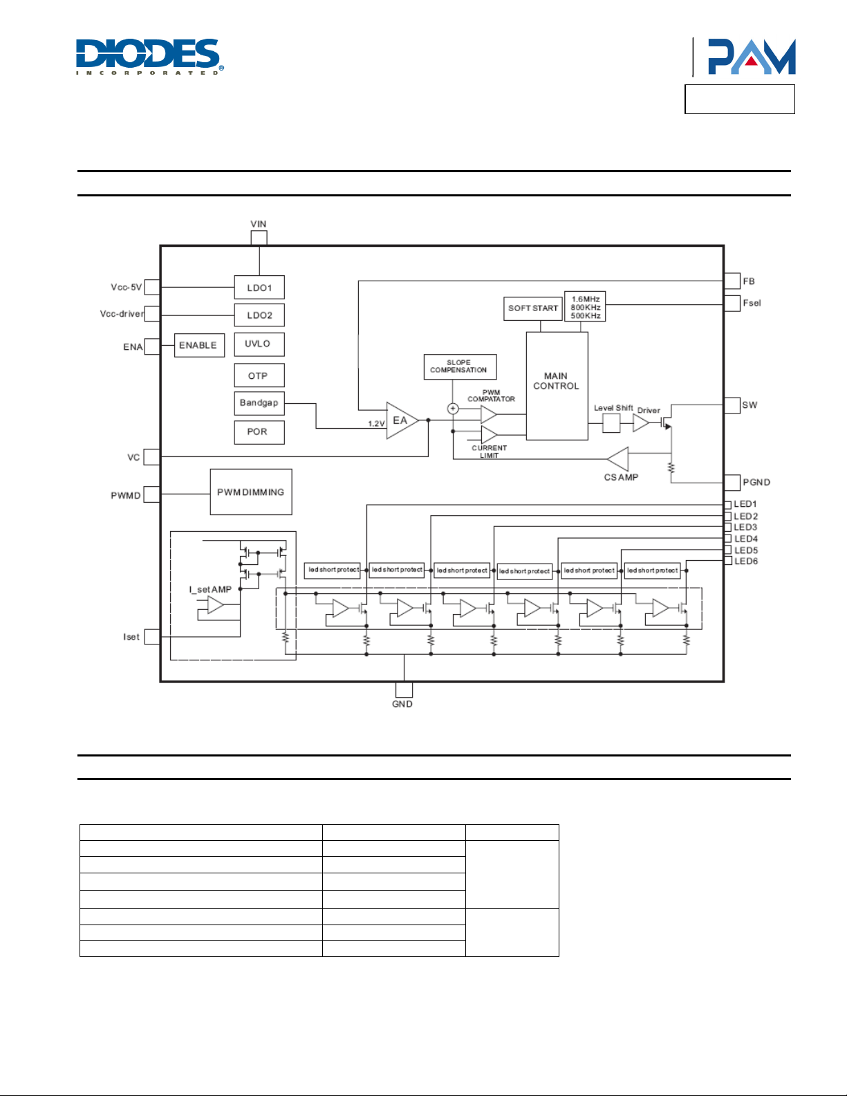
Functional Block Diagram
Product Line o
Diodes Incorporated
PAM2845
Absolute Maximum Ratings (@T
These are stress ratings only and functional operation is not implied. Exposure to absolute maximum ratings for prolonged time periods may
affect device reliability. All voltages are with respect to ground.
Parameter Rating Unit
VIN, ENA -0.3 to +30
SW, LED -0.3 to +40
VCC -5V, VCC–Driver, VC
PWMD. F
Storage Temperature -65 to +170
Maximum Junction Temperature 170
Soldering Temperature 300, 5sec
PAM2845
Document number: DSxxxxx Rev. 1 - 2
SEL
, FB, I
SET
= +25°C, unless otherwise specified.)
A
-0.3 to +6.0
-0.3 to +6.0
3 of 14
www.diodes.com
V
°C
October 2012
© Diodes Incorporated
Page 4
A
f
Product Line o
Diodes Incorporated
PAM2845
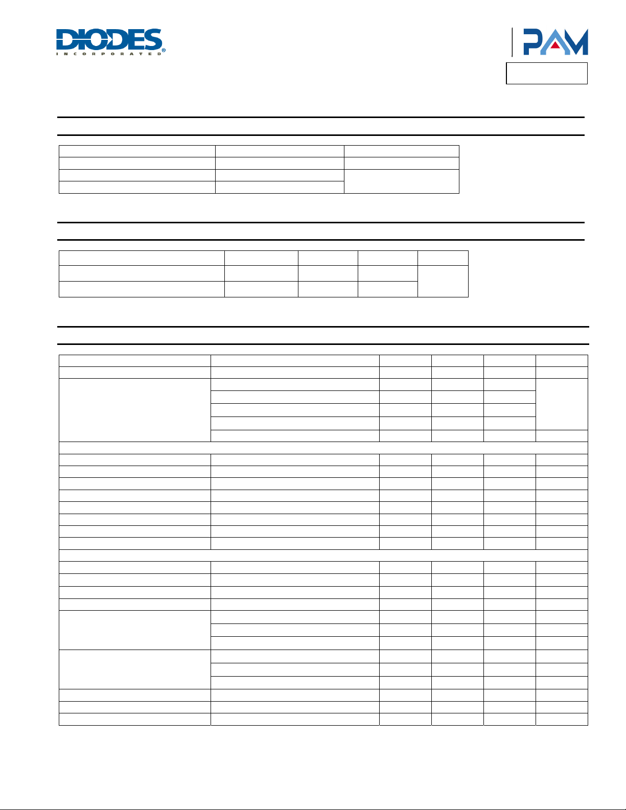
Recommended Operating Conditions (@T
Parameter Rating Unit
Supply Voltage Range 4.8 to 28 V
Operation Temperature Range -40 to +85
Junction Temperature Range -40 to +150
= +25°C, unless otherwise specified.)
A
°C
Thermal Information
Parameter Package Symbol Max Unit
Thermal Resistance (Junction to Case)
Thermal Resistance (Junction to Ambient)
Electrical Characteristics (@T
Parameter Test Conditions Min Typ Max Units
Input Voltage Range 4.8 28 V
Quiescent Current
VDD_5V 4.5 5 5.5 V
VDD_5V Current Limit 14 74 90 mA
VDD_5V UVLO Threshold 3.9 4.2 4.5 V
VDD_5V UVLO Hysteresis 40 mV
VDD_Driver 4.5 5 5.5 V
VDD_Driver Current_Limit 14 74 90 mA
VDD_Driver UVLO Threshold 3.9 4.2 4.5 V
VDD_Driver UVLO Hysteresis 70 mV
Feedback Voltage 1.2 V
Switch RDS(ON)
Switch Current Limit 2.5 A
Switch Leakage Current 1 µA
Switching Frequency
Minimum Duty Cycle
Maximum Duty Cycle 90 %
VC Source Current 60 µA
VC Sink Current 60 µA
PAM2845
Document number: DSxxxxx Rev. 1 - 2
QFN4x4-24
QFN4x4-24
= +25°C, VIN = ENA = 12V, L = 22µH, R
A
E NA = high (no switching frequency) 1 2
F
= high (1.6M switching frequency)
SEL
F
= high (1M switching frequency)
SEL
F
= high (500k switching frequency)
SEL
E NA = low 5 20 µA
V
_5V = 5V
CC
F
= VCC_5V
SEL
F
= Open
SEL
F
= GND
SEL
= VCC_5V
F
SEL
F
= Open
SEL
F
= GND
SEL
www.diodes.com
θ
JC
θ
JA
LDO Stage
Boost Stage
4 of 14
12
30
= 10kΩ, unless otherwise specified.)
SET
°C/W
10
6
3
0.2 Ω
1.6 MHz
1.0 MHz
500 kHz
20 %
10 %
5 %
October 2012
© Diodes Incorporated
mA
Page 5
A
f
Product Line o
Diodes Incorporated
PAM2845
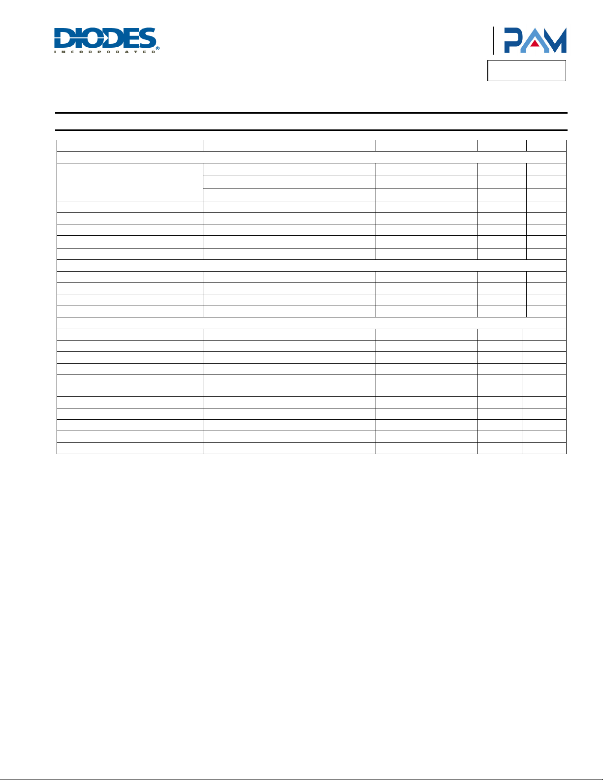
Electrical Characteristics (cont.) (@T
Parameter Test Conditions Min Typ Max Units
I = 190*1.2V/R
Full-Scale LED_Output Current
LED Current Matching -3 1 +3 %
ISET Voltage 1.2 V
Minimums LED Voltage 400 mV
Analog Dimming Range
PWM Dimming Frequency 100 1k Hz
LED_Overvoltage Threshold 4.6 4.9 5.1 V
LED_Overvoltage Hysteresis 1 V
Thermal-Shutdown 150 °C
Thermal-Shutdown Hysteresis 30 °C
EN High 1.5 V
EN Low 0.4 V
PWMD High 1.5 V
PWMD Low 0.4 V
FSEL High
FSEL Midlevel 1 2 V
FSEL Low 0.5 V
EN Min Pulse Width 0.5 µs
EN Max Pulse Width 10 µs
EN Off Delay 10 µs
PAM2845
Document number: DSxxxxx Rev. 1 - 2
I = 190*1.2V/R
I = 190*1.2V/R
I = 190*1.2V/R
= +25°C, VIN = ENA = 12V, L = 22µH, R
A
LED Controller Stage
, R
ISET
ISET
ISET
ISET
= 7.68k
ISET
, R
= 11.3k
ISET
, R
= 22.6k
ISET
Fault Protection
Control Interface
5 of 14
www.diodes.com
= 10kΩ, unless otherwise specified.)
SET
30 mA
20 mA
10 mA
I/32 I mA
_5V -
V
CC
0.5
V
October 2012
© Diodes Incorporated
Page 6

A
f
Typical Performance Characteristics
(@TA = +25°C, VIN = ENA = 12V, L = 22µH, R
= 10kΩ, unless otherwise specified.)
SET
Product Line o
Diodes Incorporated
PAM2845
PAM2845
Document number: DSxxxxx Rev. 1 - 2
6 of 14
www.diodes.com
October 2012
© Diodes Incorporated
Page 7

A
f
Typical Performance Characteristics (cont.)
(@TA = +25°C, VIN = ENA = 12V, L = 22µH, R
= 10kΩ, unless otherwise specified.)
SET
Product Line o
Diodes Incorporated
PAM2845
PAM2845
Document number: DSxxxxx Rev. 1 - 2
7 of 14
www.diodes.com
October 2012
© Diodes Incorporated
Page 8

A
f
Typical Performance Characteristics (cont.)
(@TA = +25°C, VIN = ENA = 12V, L = 22µH, R
= 10kΩ, unless otherwise specified.)
SET
Product Line o
Diodes Incorporated
PAM2845
PAM2845
Document number: DSxxxxx Rev. 1 - 2
8 of 14
www.diodes.com
October 2012
© Diodes Incorporated
Page 9

A
f
Product Line o
Diodes Incorporated
PAM2845
Application Information
The inductance, peak current rating, series resistance, and physical size should all be considered when selecting an inductor. These factors
affect the converter's operating mode, efficiency, maximum output load capability, transient response time, output voltage ripple, and cost.
The maximum output current, input voltage, output voltage, and switching frequency determine the inductor value. Very high inductance
minimizes the current ripple, and therefore reduces the peak current, which decreases core losses in the inductor and I
power path. However, large inductor values also require more energy storage and more turns of wire, which increases physical size and I
copper losses in the inductor. Low inductor values decrease the physical size, but increase the current ripple and peak current. Finding the best
inductor involves the compromises among circuit efficiency, inductor size, and cost.
When choosing an inductor, the first step is to determine the operating mode: continuous conduction mode (CCM) or discontinuous conduction
mode (DCM). When CCM mode is chosen, the ripple current and the peak current of the inductor can be minimized. If a small-size inductor is
required, DCM mode can be chosen. In DCM mode, the inductor value and size can be minimized but the inductor ripple current and peak
current are higher than those in CCM.
Capacitor Selection
An input capacitor is required to reduce the input ripple and noise for proper operation of the PAM2845. For good input decoupling, Low ESR
(equivalent series resistance) capacitors should be used at the input. At least 2.2µF input capacitor is recommended for most applications. A
minimum output capacitor value of 10µF is recommended under normal operating conditions, while a 22µF or higher capacitor may be required
for higher power LED current. A reasonable value of the output capacitor depends on the LED current. The total output voltage ripple has two
components: the capacitive ripple caused by the charging and discharging on the output capacitor, and the ohmic ripple due to the capacitor's
equivalent series resistance. The ESR of the output capacitor is the important parameter to determine the output voltage ripple of the converter,
so low ESR capacitors should be used at the output to reduce the output voltage ripple. The voltage rating and temperature characteristics of the
output capacitor must also be considered. So a value of 10µF, voltage rating (50V) capacitor is chosen.
Diodes Selection
PAM2845 is high switching frequency convertor, which demands high speed rectifier. It's indispensable to use a Schottky diode rated at 2A, 60V
with the PAM2845. Using a Schottky diode with a lower forward voltage drop is better to improve the power LED efficiency, and its voltage rating
should be greater than the output voltage.
Methods for Setting LED Current
There are three methods for setting and adjusting the LED current outlined here. The methods are:
1) RSET
2) PWM Input at PWMD
3) PWM Input at ENA
2
R losses in the entire
2
R
PAM2845
Document number: DSxxxxx Rev. 1 - 2
Figure 1
9 of 14
www.diodes.com
October 2012
© Diodes Incorporated
Page 10

A
f
Application Information (cont.)
Product Line o
Diodes Incorporated
PAM2845
• Method 1: LED Current Setting with External Resistor R
The most basic means of setting the LED current is connecting a resistor between R
I
= 228/ R
LED
ISET
ISET
and GND. The LED current is decided by I
ISET
Resistor.
SET
• Method 2: LED Current Setting Using PWM Signal to PWMD Pin
This circuit uses resistor R
PWMD pin is logic low. Average LED current is approximately equal to:
I = (t
*I)/ (tON + t
ON
Also, the recommended PWM frequency is between 100Hz and 1kHz. Frequency <100Hz can cause the LEDs to blink visibly.
to set the on state current and the average LED current, then proportional to the percentage of on-time when the
ISET
)
OFF
• Method 3: LED Current Setting with Single Wire Logic to ENA Pin
When the LEDs are enabled by high level, the LED current initially goes to I
width). Each pulse reduces the LED current by 1/32, so after one pulse the LED current is 31/32*I
.
to I
LED
Figure 1 shows a timing diagram for EN.
. Dimming is done by pulsing ENA low (500ns to 10µs pulse
LED
. The 32th pulse sets the LED current back
LED
Setting the Output Voltage
The FB pin is connected to the center tap of a resistive voltage divider (R1 and R2 in Figure 1) from the high-voltage output.
V
The recommend procedure is to choose R2 = 300kΩ and R1 = 9.2kΩ to set V
Generally the V
= 33V.
V
LED
One or more of the LED1 - 6 pins could be floating if not used because the PAM2845 uses external resistor to set the output voltage. One or
more LEDx pins floating is just like change of output loadings.
LED Short Protection
The PAM2845 uses LED FB function to protect devices when one or more LED(s) is/are shorted.
V
Normally V
make sure all LED pins’ voltage is less then 5V. With this function V
Note:
V
: LED pin voltage
LED
: Output voltage
V
OUT
: LED forward voltage
V
f
: The minimum LED numbers among all strings.
N
MIN
= VFB (1 + R2/R1)
OUT
must be higher than total LED voltage. For 10-LED application, R1 = 9.1kΩ, R2 = 270kΩ, V
OUT
= V
LED
LED
– VfN
OUT
is around 0.4V and V
= 40V.
OUT(MAX)
= 36.8V, higher than
OUT
is decided by LED numbers. When one or more LED(s) is/are shorted, the PAM2845 will clamp V
OUT
will be clamped at (5V+ VfN
OUT
MIN
).
OUT
to
PAM2845
Document number: DSxxxxx Rev. 1 - 2
10 of 14
www.diodes.com
October 2012
© Diodes Incorporated
Page 11

A
f
Product Line o
Diodes Incorporated
PAM2845
Application Information (cont.)
PCB Layout Guidelines
Careful PCB layout is important for proper operation. Use the following guidelines for good PCB layout:
1) Minimize the area of the high current switching loop of the rectifier diode and output capacitor to avoid excessive switching noise.
2) Connect high-current input and output components with short and wide connections. The high-current input loop goes from the positive
terminal of the input capacitor to the inductor, to the SW pin. The high-current output loop is from the positive terminal of the input capacitor
through the inductor, rectifier diode, and positive terminal of the output capacitors, reconnecting between the output capacitor and input
capacitor ground terminals. Avoid using vias in the high-current paths. If vias are unavoidable, use multiple vias in parallel to reduce resistance
and inductance.
3) Create a ground island (PGND) consisting of the input and output capacitor ground and PGND pin. Connect all these together with short, wide
traces or a small ground plane. Maximizing the width of the power ground traces improves efficiency and reduces output-voltage ripple and
noise spikes. Create an analog ground island (GND) consisting of the output voltage detection-divider ground connection, the I resistor
connections, VCC-5V and VCC-driver capacitor connections, and the device's exposed backside pad. Connect the GND and PGND islands by
connecting the GND pins directly to the exposed backside pad. Make sure no other connections between these separate ground planes.
4) Place the output voltage setting-divider resistors as close to the OVP pin as possible. The divider's center trace should be kept short. Avoid
running the sensing traces near SW Pin.
5) Place the VIN pin bypass capacitor as close to the device as possible. The ground connection of the VIN bypass capacitor should be
connected directly to GND pins with a wide trace.
6) Minimize the size of the SW node while keeping it wide and short. Keep the SW node away from the feedback node and ground. If possible,
avoid running the SW node from one side of the PCB to the other.
7) Refer to the PAM2845 Evaluation board for an example of proper board layout.
PAM2845 Evaluation Board
PAM2845
Document number: DSxxxxx Rev. 1 - 2
11 of 14
www.diodes.com
October 2012
© Diodes Incorporated
Page 12

A
f
Ordering Information
Product Line o
Diodes Incorporated
PAM2845
Part Number Package Type Standard Package
PAM2845KHR QFN4x4-24 3000 Units/Tape&Reel
Marking Information
PAM2845
Document number: DSxxxxx Rev. 1 - 2
12 of 14
www.diodes.com
October 2012
© Diodes Incorporated
Page 13

A
f
Package Outline Dimensions (All dimensions in mm.)
QFN4x4-24
Product Line o
Diodes Incorporated
PAM2845
PAM2845
Document number: DSxxxxx Rev. 1 - 2
13 of 14
www.diodes.com
October 2012
© Diodes Incorporated
Page 14

A
f
Product Line o
Diodes Incorporated
PAM2845
DIODES INCORPORATED MAKES NO WARRANTY OF ANY KIND, EXPRESS OR IMPLIED, WITH REGARDS TO THIS DOCUMENT,
INCLUDING, BUT NOT LIMITED TO, THE IMPLIED WARRANTIES OF MERCHANTABILITY AND FITNESS FOR A PARTICULAR PURPOSE
(AND THEIR EQUIVALENTS UNDER THE LAWS OF ANY JURISDICTION).
Diodes Incorporated and its subsidiaries reserve the right to make modifications, enhancements, improvements, corrections or other changes
without further notice to this document and any product described herein. Diodes Incorporated does not assume any liability arising out of the
application or use of this document or any product described herein; neither does Diodes Incorporated convey any license under its patent or
trademark rights, nor the rights of others. Any Customer or user of this document or products described herein in such applications shall assume
all risks of such use and will agree to hold Diodes Incorporated and all the companies whose products are represented on Diodes Incorporated
website, harmless against all damages.
Diodes Incorporated does not warrant or accept any liability whatsoever in respect of any products purchased through unauthorized sales channel.
Should Customers purchase or use Diodes Incorporated products for any unintended or unauthorized application, Customers shall indemnify and
hold Diodes Incorporated and its representatives harmless against all claims, damages, expenses, and attorney fees arising out of, directly or
indirectly, any claim of personal injury or death associated with such unintended or unauthorized application.
Products described herein may be covered by one or more United States, international or foreign patents pending. Product names and markings
noted herein may also be covered by one or more United States, international or foreign trademarks.
This document is written in English but may be translated into multiple languages for reference. Only the English version of this document is the
final and determinative format released by Diodes Incorporated.
Diodes Incorporated products are specifically not authorized for use as critical components in life support devices or systems without the express
written approval of the Chief Executive Officer of Diodes Incorporated. As used herein:
A. Life support devices or systems are devices or systems which:
1. are intended to implant into the body, or
2. support or sustain life and whose failure to perform when properly used in accordance with instructions for use provided in the
labeling can be reasonably expected to result in significant injury to the user.
B. A critical component is any component in a life support device or system whose failure to perform can be reasonably expected to cause the
failure of the life support device or to affect its safety or effectiveness.
Customers represent that they have all necessary expertise in the safety and regulatory ramifications of their life support devices or systems, and
acknowledge and agree that they are solely responsible for all legal, regulatory and safety-related requirements concerning their products and any
use of Diodes Incorporated products in such safety-critical, life support devices or systems, notwithstanding any devices- or systems-related
information or support that may be provided by Diodes Incorporated. Further, Customers must fully indemnify Diodes Incorporated and its
representatives against any damages arising out of the use of Diodes Incorporated products in such safety-critical, life support devices or systems.
Copyright © 2012, Diodes Incorporated
www.diodes.com
IMPORTANT NOTICE
LIFE SUPPORT
PAM2845
Document number: DSxxxxx Rev. 1 - 2
14 of 14
www.diodes.com
October 2012
© Diodes Incorporated
 Loading...