

Page 1
A
f
Description
The PAM2842 is a high power LED driver, capable of driving up to 10
high power LEDs in series. The PAM2842 supports buck, boost and
sepic topology.
The PAM2842 features over current protection, over voltage
protection, under voltage lockout and over temperature protection,
which prevent the device from damage.
LED dimming can be done by using a PWM signal to the COMP pin.
The PAM2842 is available in TSSOP-20 packages.
Features
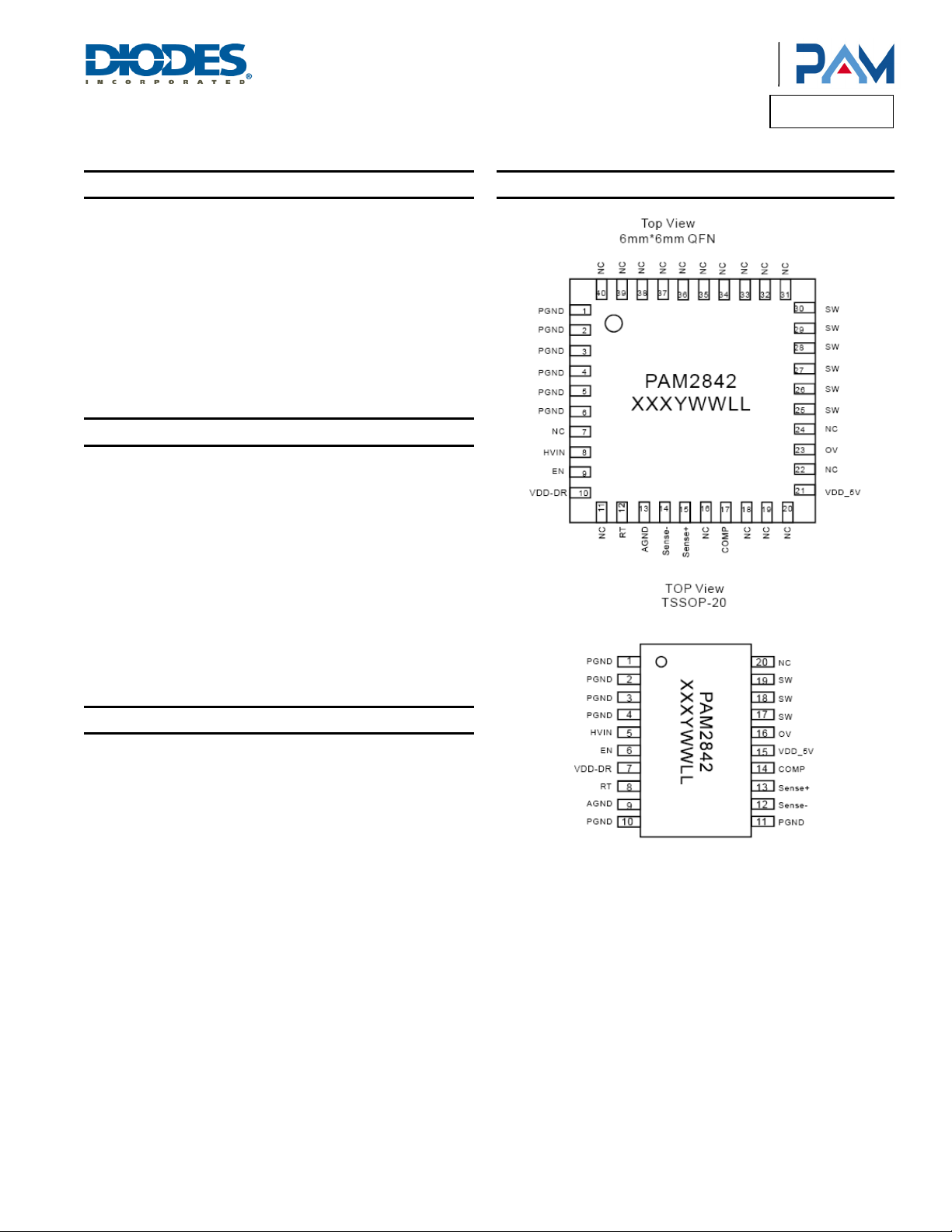
Pin Assignments
Product Line o
Diodes Incorporated
PAM2842
HIGH POWER LED DRIVER
• Output Power up to 30W
• Chip Enable with Soft-start
• Analog and PWM Dimming
• Peak Efficiency up to 97%
• Low Quiescent Current
• Switching Frequency Adjustable
• Support Buck/Boost/Sepic Toplogy
• Over Current Protection
• Over Voltage Protection
• Thermal Protection
• UVLO
• Tiny Pb-Free Packages: 40-Pin QFN6x6 and TSSOP-20
Applications
• Home Lighting
• Automotive Lighting
• Monitor Backlighting
PAM2842
Document number: DSxxxxx Rev. 1 - 2
1 of 17
www.diodes.com
October 2012
© Diodes Incorporated
Page 2
A
f
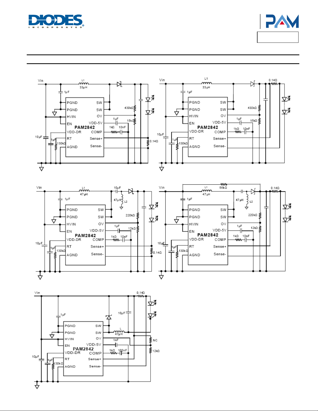
Typical Applications Circuit
Boost with Low Side Current Sense Boost with High Side Current Sense
Product Line o
Diodes Incorporated
PAM2842
Buck/Boost (Sepic) with Low Side Current Sense Buck/Boost (Sepic) with High Side Current Sense
Buck with High Side Current Sense
PAM2842
Document number: DSxxxxx Rev. 1 - 2
2 of 17
www.diodes.com
October 2012
© Diodes Incorporated
Page 3
A
f
Pin Descriptions
Pin
Name
QFN6x6-40 TSSOP-20
Pin Number
PGND 1 – 6 1, 2, 3, 4, 10, 11
HVIN 8 5
EN 9 6
VDD-DR 10 7
RT 12 8
AGND 13 9
Sense- 14 12
Sense+ 15 13
COMP 17 14
VDD_5V 21 15
OV 23 16
SW 25 – 30 17, 18, 19
NC
7, 11, 16, 18-20,
22, 24, 31-40
20
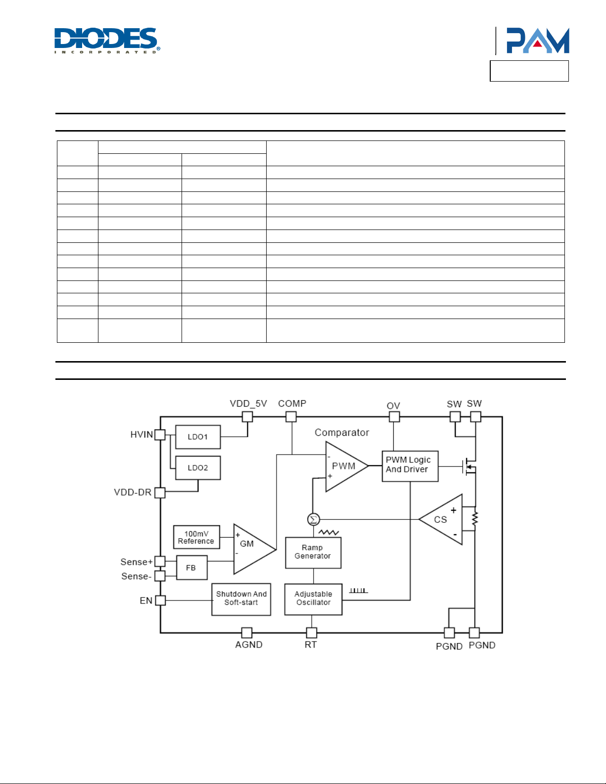
Functional Block Diagram
Product Line o
Diodes Incorporated
PAM2842
Function
Power Ground
Input
Chip Enable, Active High
Internal LDO Output
Frequency Adjustment Pin
Analog Ground
Sense Resistor -
Sense Resistor+
Compensation Node
Internal LDO Output
Over Voltage
Drain of Main Switch
Not Connected
PAM2842
Document number: DSxxxxx Rev. 1 - 2
3 of 17
www.diodes.com
October 2012
© Diodes Incorporated
Page 4
A
f
Product Line o
Diodes Incorporated
PAM2842
Absolute Maximum Ratings (@T
These are stress ratings only and functional operation is not implied. Exposure to absolute maximum ratings for prolonged time periods may
affect device reliability. All voltages are with respect to ground.
Parameter Rating Unit
Supply Voltage 40 V
Buck Application Maximum Output Current 3 A
I/O Pin Voltage Range
Maximum Junction Temperature 150
Storage Temperature -40 to +150
Soldering Temperature 300, 5sec
Recommended Operating Conditions (@T
Parameter Rating Unit
Supply Voltage Range 5.5 to 40 V
Operation Temperature Range -40 to +85
Junction Temperature Range -40 to +125
= +25°C, unless otherwise specified.)
A
GND -0.3 to V
A
+0.3
DD
= +25°C, unless otherwise specified.)
V
°C
°C
Thermal Information
Parameter Package Symbol Max Unit
Thermal Resistance (Junction to Case)
Thermal Resistance (Junction to Ambient)
Note: 1. The exposed PAD must be soldered to a thermal land on the PCB.
Electrical Characteristics (@T
Parameter Test Conditions Min Typ Max Units
Input Voltage Range 5.5 40 V
Quiescent Current
Feedback Voltage, Low Side
Feedback Voltage, High Side
LED Current Line Regulation
LED Current Load Regulation 1.0 %
VDD_DR UVLO Hysteresis No Switching 200 mV
PAM2842
Document number: DSxxxxx Rev. 1 - 2
TSSOP-20
QFN6x6-40 7.6 (Note 1)
TSSOP-20
QFN6x6-40 18.1 (Note 1)
= +25°C, VEN = VDD = 24V, 1W x 10 LEDs, unless otherwise specified.)
A
E NA = high (no switching frequency) 1 2 mA
E NA = high (1M switching frequency) 6 mA
E NA = high (500k switching frequency) 3 mA
E NA = high (200k switching frequency) 1.6 mA
E NA = low 5 10 µA
V
= V
FB
V
= V
FB
I
= 350mA
O
SENSE+
SENSE+
-AGND, V
– V
SENSE-
www.diodes.com
SENSE-
4 of 17
θ
JC
θ
JA
= AGND
20
90
95 100 105 mV
95 100 105 mV
°C/W
0.02 %/V
October 2012
© Diodes Incorporated
Page 5
A
f
Product Line o
Diodes Incorporated
PAM2842
Electrical Characteristics (cont.) (@T
Parameter Test Conditions Min Typ Max Units
VDD_5V No Switching 4.5 5 5.5 V
VDD_5V Current Limit No Switching 14 74 90 mA
VDD_5V UVLO Threshold No Switching 3.7 4.0 4.3 V
VDD_5V UVLO Hysteresis No Switching 200 mV
VDD_DR No Switching 4.5 5 5.5 V
VDD_DR Current_Limit No Switching 14 50 90 mA
VDD_DR UVLO Threshold No Switching 3.7 4.0 4.3 V
Switch RDS(ON) VDD_5V = 5V 0.1 Ω
Switch Current Limit 3.5 A
Switch Leakage Current 50 µA
RT Voltage
Switching Frequency (Note 2)
Min Duty Cycle
Max Duty Cycle
VC Source Current Feedback Voltage = 0 30 µA
VC Sink Current Feedback Voltage = 0 30 µA
OV Threshold Voltage 1.1 1.2 1.3 V
OV Hysteresis 70 mV
Thermal Shutdown 150 °C
Thermal Shutdown Hysteresis 30 °C
EN High 1.5 V
EN Low 0.4 V
Note: 2. Switching frequency
F
SW
PAM2842
Document number: DSxxxxx Rev. 1 - 2
R
RT
R
RT
RRT = 71kΩ
RRT = 180kΩ
F
SW
FSW = 500kHz
FSW = 200kHz
Low Side Sense 95 %
High Side Sense 100 %
10
=
(x24
R
= +25°C, VEN = VDD = 24V, 1W x 10 LEDs, unless otherwise specified.)
A
LDO Stage
Switch Stage
= 71kΩ
= 30kΩ
= 1MHz
12
+
RT
Fault Protection
Control Interface
, reference value.
)k12
www.diodes.com
5 of 17
1.1 1.2 1.3 V
800k 1M 1.2M Hz
400 500 600 kHz
160 200 240 kHz
10 %
5 %
2.5 %
October 2012
© Diodes Incorporated
Page 6
A
f
Diodes Incorporated
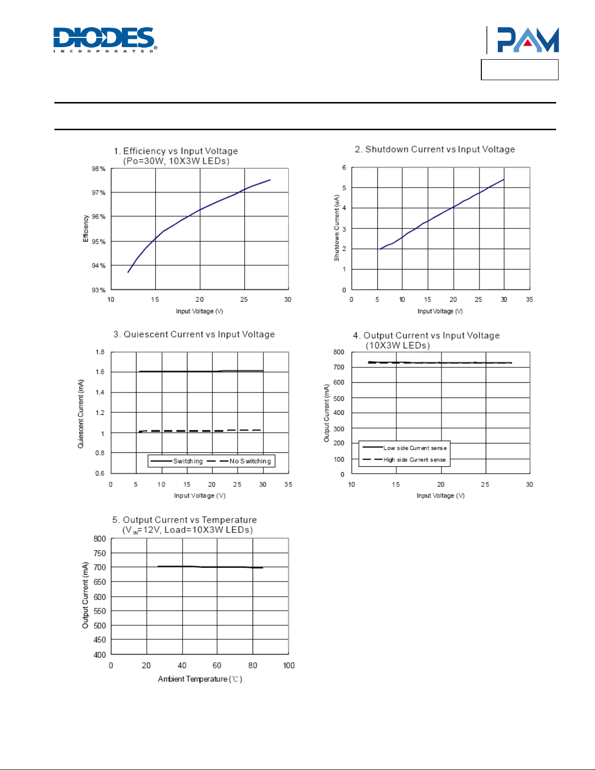
Typical Performance Characteristics
Boost Mode, @TA = +25°C, VEN = VDD = 24V, 3W LEDs, FSW = 200kHz, unless otherwise specified.)
Product Line o
PAM2842
PAM2842
Document number: DSxxxxx Rev. 1 - 2
6 of 17
www.diodes.com
© Diodes Incorporated
October 2012
Page 7

A
f
Typical Performance Characteristics (cont.) @T
Product Line o
Diodes Incorporated
= +25°C, FSW = 300kHz, unless otherwise specified.)
A
PAM2842
PAM2842
Document number: DSxxxxx Rev. 1 - 2
7 of 17
www.diodes.com
© Diodes Incorporated
October 2012
Page 8

A
f
Product Line o
Diodes Incorporated
PAM2842
Application Information
Topology Selection
When maximum power supply voltage is below than minimum load voltage, select the boost topology. When minimum power supply voltage is
high than maximum load voltage, select buck topology. When load voltage range is small and between the power supply voltage, select sepic
topology.
Table 1: Voltage Condition vs. Topology
Condition Topology
V
< V
INMAX
V
> V
INMIN
VO<VIN
OMIN
OMAX
Inductor Selection
The inductance, peak current rating, series resistance, and physical size should all be considered when selecting an inductor. These factors
affect the converter's operating mode, efficiency, maximum output load capability, transient response time, output voltage ripple, and cost.
The maximum output current, input voltage, output voltage, and switching frequency determine the inductor value. Large inductance can
minimizes the current ripple, and therefore reduces the peak current, which decreases core losses in the inductor and I2R losses in the entire
power path. However, large inductor values also require more energy storage and more turns of wire, which increases physical size and I2R
copper losses in the inductor. Low inductor values decrease the physical size, but increase the current ripple and peak current. Finding the best
inductor involves the compromises among circuit efficiency, inductor size, and cost.
When choosing an inductor, the first step is to determine the operating mode: continuous conduction mode (CCM) or discontinuous conduction
mode (DCM). When CCM mode is chosen, the ripple current and the peak current of the inductor can be minimized. If a small-size inductor is
required, DCM mode can be chosen. In DCM mode, the inductor value and size can be minimized but the inductor ripple current and peak
current are higher than those in CCM.
For the large power application, if chose DCM, the peak current will be very large, it will have great electrical stress on the components, so we
chose CCM.
When work in CCM mode, a reasonable ripple current is chosen to
ΔI
For the boost topology,
D: duty cycle, Io: output current, F: switching frequency.
From above equation we can get the inductance:
The inductor's current rating should be higher
than
For the buck topology, I
so
= 0.4IL
L
=
I
L
L−=
+
I
L
=
D
I
Δ
L
L−=
I
O
D
,
D1
−
2
(V5.2
IN
FI
O
I
O
2
= IO
L
V
O
V
IN
(
−
LFV
O
FI
VV
IN
(V5.2
V
O
=
PAM2842
Document number: DSxxxxx Rev. 1 - 2
Boost
Buck
Sepic
−
VV
=
V
O
V
O
INO
,
I
V
VV
2
)
V
OOIN
IN
VV
OIN
2
Δ
O
)
INO
)
(
V
=
L
LF
)
−
VV
INOIN
V
O
www.diodes.com
8 of 17
October 2012
© Diodes Incorporated
Page 9

A
f
Product Line o
Diodes Incorporated
PAM2842
Application Information (cont.)
Inductor Selection (cont.)
For the sepic topology, L1 = L2
I
Chose
so
D
L
Capacitor Selection
An input capacitor is required to reduce the input ripple and noise for proper operation of the PAM2842. For good input decoupling, Low ESR
(equivalent series resistance) capacitors should be used at the input. At least 10µF input capacitor is recommended for most applications. And
close the IC V
A minimum output capacitor value of 10µF is recommended under normal operating conditions, while a 22µF or higher capacitor may be
required for higher power LED current. A reasonable value of the output capacitor depends on the LED current. The total output voltage ripple
has two components: the capacitive ripple caused by the charging and discharging on the output capacitor, and the ohmic ripple due to the
capacitor's equivalent series resistance. The ESR of the output capacitor is the important parameter to determine the output voltage ripple of the
converter, so low ESR capacitors should be used at the output to reduce the output voltage ripple. The voltage rating and temperature
characteristics of the Output capacitor must also be considered. So a value of 10µF, 50V voltage rating capacitor is chosen.
Consider from discharge aspect: I x Δt = C x ΔV
In boost and sepic topology,
In buck topology,
: Output voltage allowable ripple.
V
RIPPLE
Consider from equivalent series resistance:
V
In sepic topology, there is a series capacitor Cs between L1 and L2 (see application schematic), it flows the current:
The ripple voltage is
The voltage rating must be higher than input voltage.
Because the Cs capacitor will flow the large RMS current, so this topology is suitable for small power application.
RIPPLE-ESR
O
=
=
I
L
=
V =Δ
II
=Δ
IN-PIN
CS
O1L
D1
−
=
II
O2L
V
O
+
VV
OIN
VV
OIN
+
I4.0I =Δ
2
V5.2
IN
+
VV
I
O
FV
CO.RIPPLE
V
O)RMS(CS
V
D
S
)
VV
OIN
1LL
)
OIN
C
O
−
RIPPLE
O
IN
=
)D1(
x C
FV
D
I
O
RIPPLE
OESR
(LF
(FI
O
we should add a bypass capacitor, usually use a 1µF capacitor.
=
C
O
= I
=
II
I
O
FC
PAM2842
Document number: DSxxxxx Rev. 1 - 2
9 of 17
www.diodes.com
October 2012
© Diodes Incorporated
Page 10

A
f
Product Line o
Diodes Incorporated
PAM2842
Application Information (cont.)
Diode Selection
PAM2842 is a high switching frequency converter which demands high speed rectifier. It's indispensable to use a Schottky diode rated at 3A,
40V with the PAM2842. Using a Schottky diode with a lower forward voltage drop is better to improve the power LED efficiency.
In boost topology, the voltage rating should be higher than V
I
Δ
L
in sepic topology, the voltage rating should be higher than V
The average current of the diode equals to I
II
L)MAX(D
+=
2
+=
III
)PEAK(2L)PEAK(1L)MAX(D
.
O
Work Frequency Selection
PAM2842 working frequency is decided by resistor connect to the RT pin, it can be calculated by follow equation:
From the equations, we can see when working frequency is high, the inductance can be small. It's important in some size limit application. But
we should know when the working frequency is higher, the switching loss is higher too. We must pay attention to thermal dissipation in this
application.
=
F
SW
10
12
+
)Hz(
)K12RT(x24
Methods for Setting LED Current
There are two methods for setting and adjusting the LED current:
1) R
2) PWM signal with external components
a) Use the COMP pin
b) Use the Sense pin
SENSE
only
● Method 1: LED Current Setting with Resistor R
The most basic means of setting the LED current is connecting a resistor between R
Resistor R
I
For flowing the large current, must pay attention to power dissipation on the resistor.
has two positions to select: high side current sense and low side current sense. In buck topology it just has high side current sense. In
R
SENSE
other topology we recommend use low side current sense for easier PCB layout.
SENSE
LED
.
= 0.1/ R
SENSE
● Method 2: LED Current Setting with PWM Signal Using COMP Pin
This circuit uses resistor Rsense to set the on state current and the average LED current, then proportional to the percentage of off-time when
the COMP pin is logic high. Here use a invert component 2N7002 (Q1) to isolate and invert the PWM signal (See Figure 1).
and in buck topology, the voltage rating higher than VIN, the peak current is
OUT
+V
SENSE
, the peak current is
OUT
SENSE
+ and R
-. The LED current is decided by ISET
SENSE
IN
Figure 1. PWM Dimming Use COMP Pin
Average LED current is approximately equal to:
IT
=
I
AVG
PAM2842
Document number: DSxxxxx Rev. 1 - 2
LEDOFF
+
TT
OFFON
10 of 17
www.diodes.com
October 2012
© Diodes Incorporated
Page 11

A
f
Product Line o
Diodes Incorporated
PAM2842
Also, the recommended PWM frequency is between 100Hz and 200Hz.
Application Information (cont.)
● Method 2: LED Current Setting with PWM Signal Using COMP Pin (cont.)
Frequency <100Hz can cause the LEDs to blink visibly. As the COMP pin connects to a capacitor, it needs rise time. If frequency >200Hz, the
average LED current will have a large error when duty cycle is small (<50%).
It maybe generate the audible noise in this dimming condition.
● Method 3: LED Current Setting with PWM Signal using Sense Pin
This method is turn PWM signal to DC voltage, the output current can be adjusted. Because the LED current is a adjustable DC value, it will
cause LED color drift.
Low side current sense and high side current sense circuit is different. Please see Figure 2 and 3. It use the internal reference voltage, so PWM
dimming signal voltage is not considered, just meet the request of the MOSFET driving voltage.
Figure 2. PWM Dimming Use Sense Pin in Low Side Current Sense Figure 3. PWM Dimming Use Sense Pin in High Side Current
The RC filter (R1,R2,C1,C2) value is decided by dimming frequency, the divider resistor (R3,R4) is decided by dimming range.
Because final adjusted is a DC value, this method can avoid audible noise effectively and achieve better EMI performance than the second
method.
Sense
Setting the Output Limit Voltage
The OV pin is connected to the center tap of a resistive voltage divider from the high-voltage output to ground (see application schematic).
R
UP
R
DOWN
)
OUT_LIMIT
.
IN +VO
11 of 17
www.diodes.com
= 37.2V.
October 2012
© Diodes Incorporated
1(
+=
−
The recommend procedure is to choose R3 = 360K and R4 = 12K to set V
In boost and sepic circuit, when LED open or no load, the circuit will have no feedback, if no other measure be taken the switch voltage will be
very high and damage the switch, so this OV pin must be set carefully.
In buck circuit, the switch voltage is always small than input voltage, so the OV pin setting is not important in this condition.
This OV pin is used to limit output voltage to avoid breakdown of the switch other than to regulate output voltage. The setting value must keep
the switch voltage below 40V.
In sepic circuit, one must notice that the switch voltage equals V
This OV pin has a hysteresis voltage detect function, not latch-up function, so output voltage will have a overshoot when no load or load working
voltage is high than setting limit voltage. If the component parameter not match appropriately, the overshoot voltage will be too high and can
demage the switch.
VV
OVLIMITOUT
PAM2842
Document number: DSxxxxx Rev. 1 - 2
Page 12

A
f
=
+++
+
Application Information (cont.)
Setting the Output Limit Voltage (cont.)
Several methods can decrease the overshoot voltage:
(1) Add a small capacitor (<100pF) parallel with the up divider resistor (See Figure 4).
(2) Use external zener to clamp the output peak voltage (See Figure 5).
Product Line o
Diodes Incorporated
PAM2842
Figure 4. Add Forward Capacitor Figure 5. Use External Zener
Note: The output limit voltage must be set higher than working output voltage by a proper value, or it will work abnormal in low temperature or
some other conditions.
Short LED Function
PAM2842 is a constant current driver. When one or more LED shorted, the circuit will still work, the output voltage is decided by LED numbers.
In boost topology, make sure the output voltage is higher than input voltage; otherwise the unlimited current will directly go through supply to
LED and damage the LED.
Power Dissipation
As PAM2842 integrates a power MOSFET, the power dissipation must be considered. To a MOSFET the power loss includes 5 sections, turn on
loss, turn off loss, conduction loss, drive loss and output capacitor Coss loss.
1
P
P
=
Tr: switch rise time. Tf: switch fall time. U
Above description does not consider the IC control power, so the total power will be more than calculated value.
PAM2842 has over-temperature protection. When junction temperature is over +150°C, it will shut down and auto restart when junction
temperature decrease below +120.
In high temperature circumstance application, one must pay attention to heat dissipation, or it will shut down and restart. It is recommended to
use external heat-sink and placed near to the IC surface.
: gate drive voltage. θJA is relative with IC package, heat-sink area and air flow condition etc.
DRIVE
−
PAM2842
Document number: DSxxxxx Rev. 1 - 2
=
2
1
=
2
=
)ON(RDS
P
P
DRIVE
COSS
Q
1
=
C
2
PPP
θ=Δ
T
JA
12 of 17
www.diodes.com
2
RMS
U
G
OSS
ff
P
SWITCH
RIP
DRIVE
2
V
OUT
f
f
TVI
rOUTONTURNONTURN −−
f
TVI
rOUTONTURNOFFTURN −−
)ON(DS
f
PPP
COSSDRIVE)ON(RDSTURNEONTURNSWITCH
October 2012
© Diodes Incorporated
Page 13

A
f
Product Line o
Diodes Incorporated
PAM2842
Application Information (cont.)
PCB Layout Guidelines
Careful PCB layout is important for normal operation. Use the following guidelines for good PCB layout: (BOOST)
1) Minimize the area of the high current switching loop of the rectifier diode and output capacitor to avoid excessive switching noise.
2) Connect high-cur rent input and output components with short and wide connections. The high-current input loop goes from the positive
terminal of the input capacitor to the inductor and the SW pin. The high-current output loop is from the positive terminal of the input capacitor
through the inductor, rectifier diode, and positive terminal of the output capacitors, reconnecting between the output capacitor and input
capacitor ground terminals. Avoid using vias in the highcurrent paths. If vias are unavoidable, use multiple vias in parallel to reduce resistance
and inductance.
3) Create a ground island (PGND) consisting of the input and output capacitor ground and PGND pin. Connect all these together with short, wide
traces or a small ground plane. Maximizing the width of the power ground traces improves efficiency and reduces output-voltage ripple and
noise spikes. Create an analog ground island (AGND) consisting of the output voltage detection-divider ground connection, the Sense-pin
connection, V
connections between these separate ground planes.
4) Place the output voltage setting-divider resistors as close to the OV pin as possible. The divider's center trace should be kept short. Avoid
running the sensing traces near SW Pin.
5) Place the VIN pin bypass capacitor as close to the device as possible. The ground connection of the VIN bypass capacitor should be
connected directly to GND pins with a wide trace.
6) Minimize the size of the SW node while keeping it wide and short. Keep the SW node away from the feedback node. If possible, avoid running
the SW node from one side of the PCB to the other.
7) For the good thermal dissipation, PAM2842 has a heat dissipate pad in the bottom side, it should be soldered to PCB surface. As the copper
area cannot be large in the component side, we can use multiple vias connecting to other side of the PCB.
8) Refer to the example of a PAM2842 Evaluation board layout below.
-5V and VCC-driver capacitor connections. Connect the device's exposed backside pad to PGND. Make sure no other
CC
TSSOP-20 Boost QFN6x6-40 Boost
PAM2842
Document number: DSxxxxx Rev. 1 - 2
PCB Layout Example
13 of 17
www.diodes.com
October 2012
© Diodes Incorporated
Page 14

A
f
Ordering Information
Product Line o
Diodes Incorporated
PAM2842
Part Number Package Type Standard Package
PAM2842RGR TSSOP-20 1000 Units/Tape&Reel
PAM2842TJR QFN6x6-40 1000 Units/Tape&Reel
Marking Information
PAM2842
Document number: DSxxxxx Rev. 1 - 2
14 of 17
www.diodes.com
October 2012
© Diodes Incorporated
Page 15

A
f
Package Outline Dimensions (All dimensions in mm.)
TSSOP-20
Product Line o
Diodes Incorporated
PAM2842
PAM2842
Document number: DSxxxxx Rev. 1 - 2
15 of 17
www.diodes.com
October 2012
© Diodes Incorporated
Page 16

A
f
Package Outline Dimensions (cont.) (All dimensions in mm.)
QFN6x6-40
Product Line o
Diodes Incorporated
PAM2842
PAM2842
Document number: DSxxxxx Rev. 1 - 2
16 of 17
www.diodes.com
© Diodes Incorporated
October 2012
Page 17

A
f
Product Line o
Diodes Incorporated
PAM2842
DIODES INCORPORATED MAKES NO WARRANTY OF ANY KIND, EXPRESS OR IMPLIED, WITH REGARDS TO THIS DOCUMENT,
INCLUDING, BUT NOT LIMITED TO, THE IMPLIED WARRANTIES OF MERCHANTABILITY AND FITNESS FOR A PARTICULAR PURPOSE
(AND THEIR EQUIVALENTS UNDER THE LAWS OF ANY JURISDICTION).
Diodes Incorporated and its subsidiaries reserve the right to make modifications, enhancements, improvements, corrections or other changes
without further notice to this document and any product described herein. Diodes Incorporated does not assume any liability arising out of the
application or use of this document or any product described herein; neither does Diodes Incorporated convey any license under its patent or
trademark rights, nor the rights of others. Any Customer or user of this document or products described herein in such applications shall assume
all risks of such use and will agree to hold Diodes Incorporated and all the companies whose products are represented on Diodes Incorporated
website, harmless against all damages.
Diodes Incorporated does not warrant or accept any liability whatsoever in respect of any products purchased through unauthorized sales channel.
Should Customers purchase or use Diodes Incorporated products for any unintended or unauthorized application, Customers shall indemnify and
hold Diodes Incorporated and its representatives harmless against all claims, damages, expenses, and attorney fees arising out of, directly or
indirectly, any claim of personal injury or death associated with such unintended or unauthorized application.
Products described herein may be covered by one or more United States, international or foreign patents pending. Product names and markings
noted herein may also be covered by one or more United States, international or foreign trademarks.
This document is written in English but may be translated into multiple languages for reference. Only the English version of this document is the
final and determinative format released by Diodes Incorporated.
Diodes Incorporated products are specifically not authorized for use as critical components in life support devices or systems without the express
written approval of the Chief Executive Officer of Diodes Incorporated. As used herein:
A. Life support devices or systems are devices or systems which:
1. are intended to implant into the body, or
2. support or sustain life and whose failure to perform when properly used in accordance with instructions for use provided in the
labeling can be reasonably expected to result in significant injury to the user.
B. A critical component is any component in a life support device or system whose failure to perform can be reasonably expected to cause the
failure of the life support device or to affect its safety or effectiveness.
Customers represent that they have all necessary expertise in the safety and regulatory ramifications of their life support devices or systems, and
acknowledge and agree that they are solely responsible for all legal, regulatory and safety-related requirements concerning their products and any
use of Diodes Incorporated products in such safety-critical, life support devices or systems, notwithstanding any devices- or systems-related
information or support that may be provided by Diodes Incorporated. Further, Customers must fully indemnify Diodes Incorporated and its
representatives against any damages arising out of the use of Diodes Incorporated products in such safety-critical, life support devices or systems.
Copyright © 2012, Diodes Incorporated
www.diodes.com
IMPORTANT NOTICE
LIFE SUPPORT
PAM2842
Document number: DSxxxxx Rev. 1 - 2
17 of 17
www.diodes.com
October 2012
© Diodes Incorporated
 Loading...