

Page 1
A
f
Description
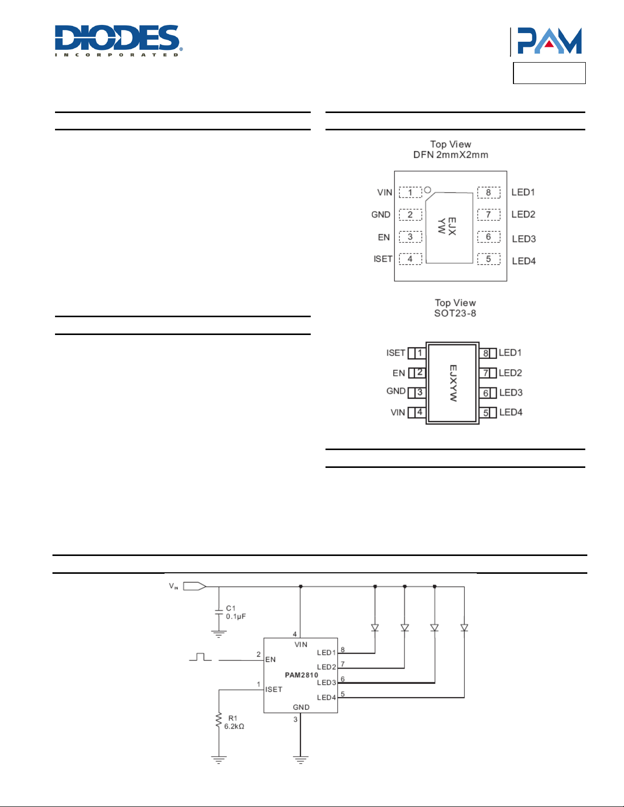
The PAM2810 provides 4 regulated current sinks, capable of sinking
up to 40mA current to accommodate 4 white LEDs. It requires no
charge pump, has no noise and EMI, and significantly improves the
efficiency in Li bettery range.
LED brightness can be controlled by PWM techniques. The constant
current sink is set with an external sense resistor.
Alternatively, a PWM signal applied to the EN pin can vary the
anticipated brightness of the LED. The device is in shut down mode
when the EN input is logic low.
The PAM2810 is available in SOT23-8 and DFN2mmx2mm
packages.
Features
4-CHANNEL PROGRAMMABLE LED CURRENT
Pin Assignments
Product Line o
Diodes Incorporated
PAM2810
• Cost Effective LED Driver
• Support up to 4 White LEDs
• Output Current up to 40mA per LED
• Low Dropout Voltage
• Ultra Low Quiescent Supply Current: 65 A (typ)
• No Noise and EMI
• Shutdown Current Less than 1 A
• Over Temperature Protection
• Small Packages : SOT23-8 and DFN2mmx2mm
• Pb-free Package
Typical Applications Circuit
Applications
• White LED for LCD Display Backlights
• White LED Keypad Backlights
• 1-Cell Li-Ion Battery-operated Equipment Including:
PDAs
Hand-Held PCs
Cellular Phone
PAM2810
Document number: DSxxxxx Rev. 1 - 1
1 of 11
www.diodes.com
October 2012
© Diodes Incorporated
Page 2
A
f
Typical Applications Circuit (cont.)
Product Line o
Diodes Incorporated
PAM2810
Pin Description
Pin
Name
VIN 1
GND 2
EN 3
ISET 4
LED4 5 5 LED4 Cathode Terminal
LED3 6 6 LED3 Cathode Terminal
LED2 7 7 LED2 Cathode Terminal
LED1 8 8 LED1 Cathode Terminal
PAM2810
Document number: DSxxxxx Rev. 1 - 1
Pin Number
DFN2x2 SOT23-8
4
3 Ground
2 Enable, Allow PWM Brightness Control, Active High
1 LED Current Adjustment Pin
Input Voltage
Function
2 of 11
www.diodes.com
October 2012
© Diodes Incorporated
Page 3
A
f
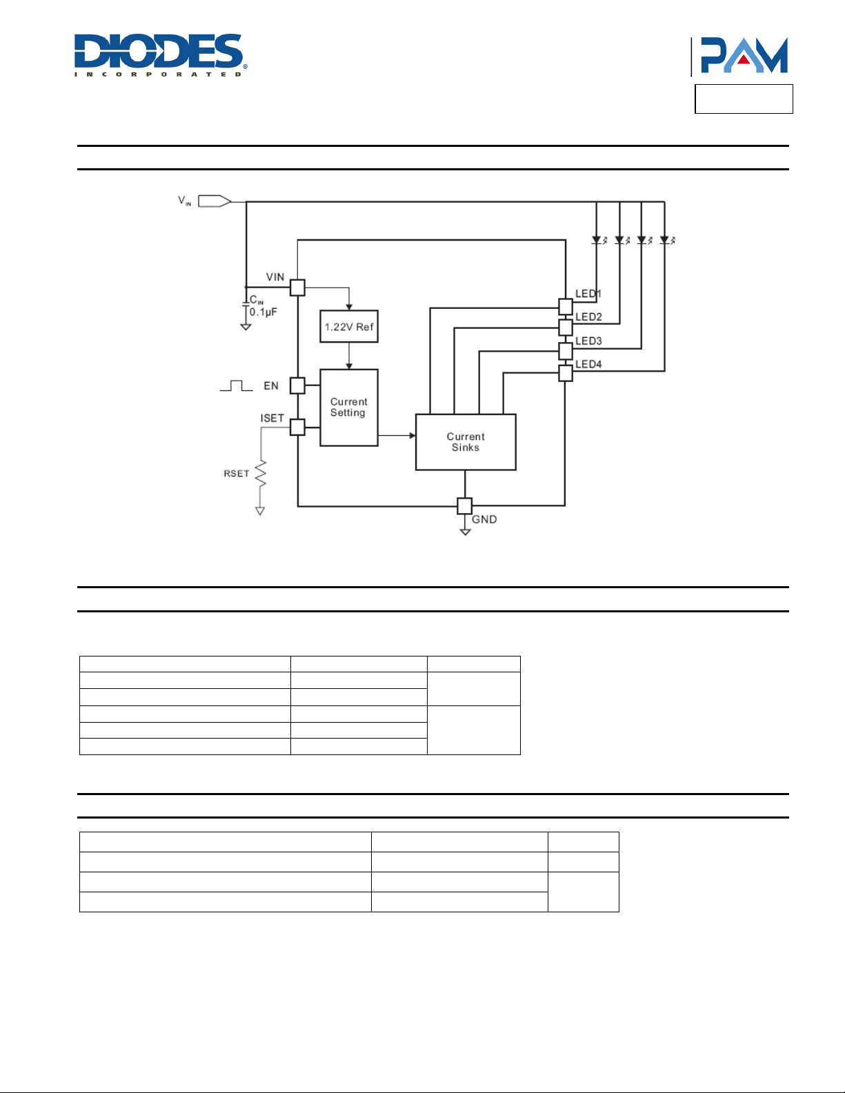
Block Diagram
Product Line o
Diodes Incorporated
PAM2810
Absolute Maximum Ratings (@T
These are stress ratings only and functional operation is not implied. Exposure to absolute maximum ratings for prolonged time periods may
affect device reliability. All voltages are with respect to ground.
Parameter Rating Unit
Input Voltage Range -0.3 to +6.0
PWM Pin Voltage
Maximum Junction Temperature 150
Storage Temperature -65 to +150
Soldering Temperature 300, 5sec
Recommended Operating Conditions (@T
Parameter Rating Unit
Input Voltage Range 2.7 to 5.5 V
Junction Temperature Range -40 to +125
Ambient Temperature Range -40 to +85
PAM2810
Document number: DSxxxxx Rev. 1 - 1
= +25°C, unless otherwise specified.)
A
-0.3 to (V
+0.3)/6V
IN
= +25°C, unless otherwise specified.)
A
www.diodes.com
3 of 11
V
°C
°C
October 2012
© Diodes Incorporated
Page 4
A
f
Product Line o
Diodes Incorporated
PAM2810
Thermal Information
Parameter Symbol Package Max Unit
Thermal Resistance (Junction to Ambient)
Thermal Resistance (Junction to Case)
θ
JA
θ
JC
Electrical Characteristics (@T
= +25°C, VIN = 3.6V, R
A
Parameter Symbol Test Conditions Min Typ Max Units
Input Voltage Range
Output Current
Current Matching Between Any Two
Outputs
Current Sink Dropout
ISET PIN Voltage
Output Current to Current Set Ratio
Quiescent Supply Current
Shutdown Supply Current
EN Input Logic High
EN Input Logic Low
EN Pin Current
V
IN
I
LEDX
I
LED-MATCH
V
DROPOUT
V
SET
I
LEDX/ISET
I
Q
I
SHDN
V
HI
V
LO
I
EN
VDD = 5V
±5 %
R
100
R
EN = Logic Low 0.1 1 µA
1.4 V
0.4 V
V(EN) = 1.5V 0.1 1 µA
V(EN) = 0V 0.1 1 µA
PAM2810
Document number: DSxxxxx Rev. 1 - 1
SOT23-8 250
DFN2x2-8 80
SOT23-8 130
DFN2x2-8 30
= 5.1kΩ, V
SET
= 0.5V, unless otherwise specified.)
LEDX
= 3kΩ, I
SET
= 10MΩ, with no loads
SET
LEDX
= 40mA
4 of 11
www.diodes.com
°C/W
Vf = V
(Note 1)
LED
3.6 5.5 V
40 mA
0.25 V
1.22 V
65 80 µA
October 2012
© Diodes Incorporated
Page 5

A
f
Typical Performance Characteristics (@T
= +25°C, VIN = 3.6V, R
A
Product Line o
Diodes Incorporated
= 5.1kΩ, V
SET
LEDX
PAM2810
= 0.5V, unless otherwise specified.)
PAM2810
Document number: DSxxxxx Rev. 1 - 1
5 of 11
www.diodes.com
© Diodes Incorporated
October 2012
Page 6

A
f
Product Line o
Diodes Incorporated
PAM2810
Application Information
The PAM2810 is a 4-channel programmable white-LED driver. The matched current regulators each have a 100:1 ratio between the LEDx
outputs and the ISET current. The PAM2810 is capable of supplying 40mA per channel with the proper selection of the external RSET resistor,
with a total of 160mA output current available. LED brightness control of PAM2810 can be achieved with a PWM signal.
Output Current Capability
The PAM2810 is capable of providing up to 40mA per LED under an input voltage of 2.7V to 5.5V. An external resistor is used to set the output
current, as approximated with the following equation:
)
DROPOUT
DROPOUT
Duty-Cycle
/V22.1(*100
I
LEDXSET
≥=−
VVVV
DROPOUTLEDXDIODEIN
Request
5.0
>
100
5
>
100
10
>
100
20
>
100
40
>
100
50
>
100
DROPOUT
www.diodes.com
can be found from the following table.
6 of 11
) must be larger than the dropout voltage of the current
LEDX
October 2012
© Diodes Incorporated
In order that the output currents could be regulated properly, the LEDx pin voltage(V
sink(V
DROPOUT
V
is the diode forward voltage, and some typical value of V
DIODE
Table 1. I
I
LED
10mA 12.7kΩ 40mV
20mA 6.2kΩ 80mV
30mA 4.3kΩ 120mV
40mA 3.2kΩ 150mV
=
R
). To ensure the desired current is obtained, apply the following equation to determine the minimum input voltage:
, R
SET
and V
V
SET
LED
R
PWM Brightness Control
Brightness control can be realized by applying a PWM signal to the EN pin. The constant current is set by the external resistor selected using the
RSET equation. The LED brightness is proportional to the duty cycle (D) of the PWM signal. The PWM frequency (f) should be limited to
accommodate the start-up time (50µs) of the device.
D * (1/f) >50µs
Table 2. PWM Frequency and Duty Cycle
Frequency Cycle
100Hz 10ms
1kHz 1ms
2kHz 500µs
4kHz 250µs
8kHz 125µs
10kHz 100µs
The maximum PWM frequency can be selected according to the table above.
If the PWM frequency is much less than 100Hz, flickering may be seen in the LEDs. For the PAM2810, zero duty cycle will turn off the LEDs and
a 50% duty cycle will result in an average ILED being half of the programmed LED current. For example, if RSET is set to program 20mA, a 50%
duty cycle will result in an average ILED of 10mA. RSET should be chosen not to exceed the maximum current capability of the device.
PAM2810
Document number: DSxxxxx Rev. 1 - 1
Page 7

A
f
Product Line o
Diodes Incorporated
PAM2810
Application Information (cont.)
Shutdown
When the EN pin is logic low, the PAM2810 will be in shutdown mode. While disabled, the PAM2810 typically draws 0.1µA current form the
power supply. There is no internal pull-up or pull-down on the EN pin.
Over Temperature Protection
The PAM2810 equips over temperature protection. When the junction temperature (TJ) exceeds +150°C, the current source turns off
automatically. The device will turn on again after the IC’s T
recommended.
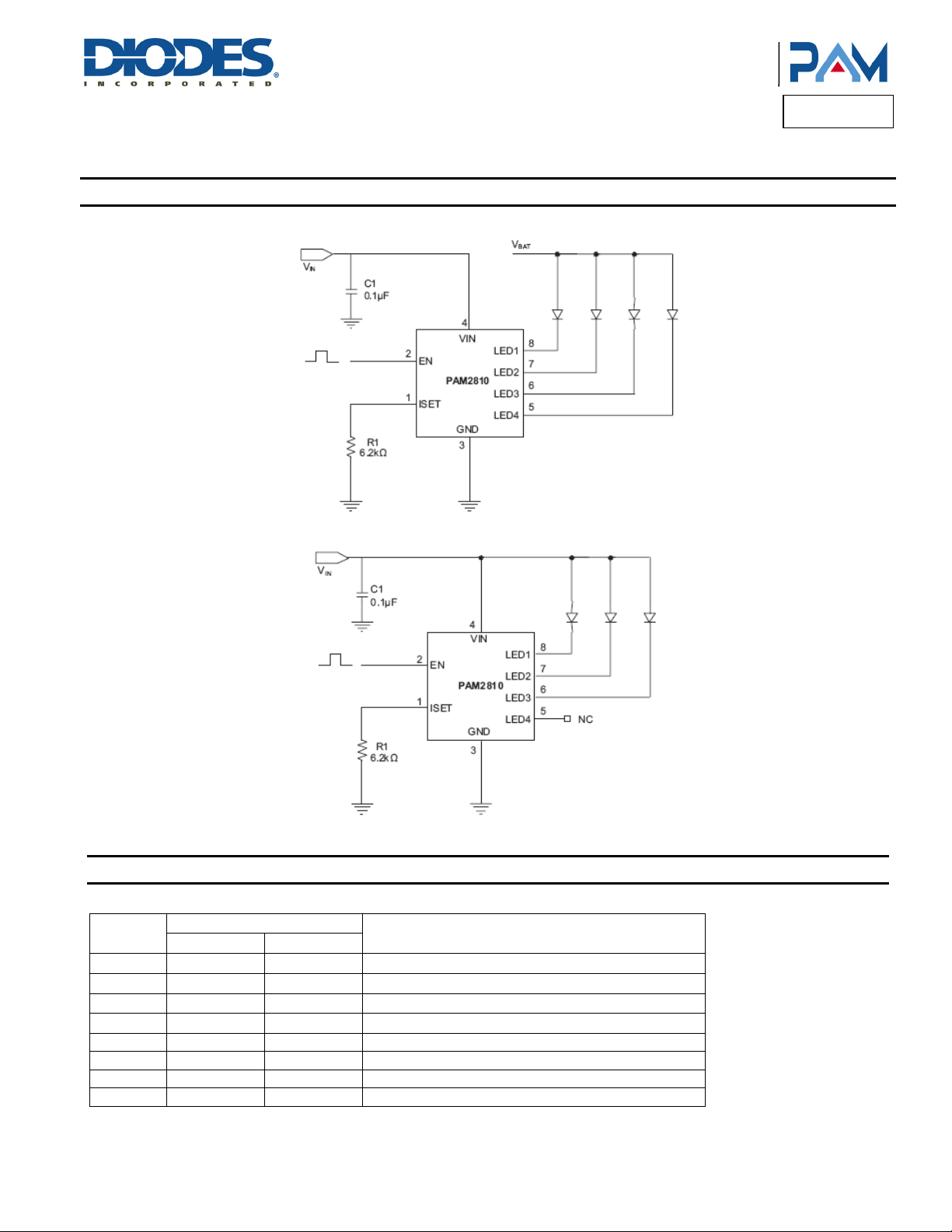
Parallel LEDx Outputs for Increased Current Drive
Output pins LED1 to LED4 may be connected together in any combination to sink higher current through fewer LEDs. For example in Figure 1,
outputs LED1 and LED2 are connected together to drive one LED while LED3 and LED4 are connected together to drive a second LED.
cools down under +125°C. Operating at absolute maximum temperature is not
J
Figure 1. Two Parallel Conneted LEDs
With this configuration, two parallel current sinks of equal value both provide current to each LED. If the current sink provides 10mA each, every
LED can be drived with 20mA and gets double brightness. Other combinations of parallel outputs can be implemented similarly, such as in
Figure 2.
Figure 2. One Parallel Connected LED
Connecting outputs in parallel does not affect internal operation of the PAM2810 and has no impact on the electrical characteristics.
If less than four LEDs connected, the left pin can be floating or connected to GND, as shown in Typical Application Circuit on Page 2.Connecting
to GND is recommended. The current calculating method is the same as the RSET equation mentioned.
PAM2810
Document number: DSxxxxx Rev. 1 - 1
7 of 11
www.diodes.com
October 2012
© Diodes Incorporated
Page 8

A
f
Product Line o
Diodes Incorporated
Application Information (cont.)
Power Dissipation
The maximum allowable power dissipation that the package is capable of handling can be determined as follows:
R
(
/)
θ−=
TT
A)MAX(JDMAX
JA
PAM2810
Where T
specified package. The DFN 2x2 package has a θ
of the PCB. The actual power dissipated by the PAM2810 follows the equation:
Where N equals the number of active outputs, V
is the maximum junction temperature, TA is the ambient temperature, and θJA is the junction-to-ambient thermal resistance of the
J(MAX)
of 80°C/W and the SOT23-8 250°C/W. This value of θJA is highly dependant upon the layout
JA
)
(
P
V
(N)I*
−=
V
*
I
LEDXDIODEININDISS
is the LED forward voltage, and I
DIODE
is the current supplied to the LEDx.
LEDX
Input Capacitor Selection
The PAM2810 is designed to work under a stable input voltage. To ensure the stability of input, it may be necessary to add a small input
capacitor to help filter out any noise that probably appears on the line. Surface-mount multi-layer ceramic capacitors are recommended, which
are small and inexpensive. A capacitance of 0.1µF is typically sufficient.
Ordering Information
Part Number Marking Package Type Standard Package
PAM2810AG EJXYW DFN 2x2-8 3000 Units/Tape&Reel
PAM2810BA EJXYW SOT23-8 3000 Units/Tape&Reel
PAM2810
Document number: DSxxxxx Rev. 1 - 1
8 of 11
www.diodes.com
October 2012
© Diodes Incorporated
Page 9

A
f
Marking Information
Product Line o
Diodes Incorporated
PAM2810
Package Outline Dimensions (All dimensions in mm.)
SOT23-8
PAM2810
Document number: DSxxxxx Rev. 1 - 1
9 of 11
www.diodes.com
October 2012
© Diodes Incorporated
Page 10

A
f
Package Outline Dimensions (cont.) (All dimensions in mm.)
DFN 2x2
Product Line o
Diodes Incorporated
PAM2810
PAM2810
Document number: DSxxxxx Rev. 1 - 1
10 of 11
www.diodes.com
October 2012
© Diodes Incorporated
Page 11

A
f
Product Line o
Diodes Incorporated
PAM2810
DIODES INCORPORATED MAKES NO WARRANTY OF ANY KIND, EXPRESS OR IMPLIED, WITH REGARDS TO THIS DOCUMENT,
INCLUDING, BUT NOT LIMITED TO, THE IMPLIED WARRANTIES OF MERCHANTABILITY AND FITNESS FOR A PARTICULAR PURPOSE
(AND THEIR EQUIVALENTS UNDER THE LAWS OF ANY JURISDICTION).
Diodes Incorporated and its subsidiaries reserve the right to make modifications, enhancements, improvements, corrections or other changes
without further notice to this document and any product described herein. Diodes Incorporated does not assume any liability arising out of the
application or use of this document or any product described herein; neither does Diodes Incorporated convey any license under its patent or
trademark rights, nor the rights of others. Any Customer or user of this document or products described herein in such applications shall assume
all risks of such use and will agree to hold Diodes Incorporated and all the companies whose products are represented on Diodes Incorporated
website, harmless against all damages.
Diodes Incorporated does not warrant or accept any liability whatsoever in respect of any products purchased through unauthorized sales
channel.
Should Customers purchase or use Diodes Incorporated products for any unintended or unauthorized application, Customers shall indemnify and
hold Diodes Incorporated and its representatives harmless against all claims, damages, expenses, and attorney fees arising out of, directly or
indirectly, any claim of personal injury or death associated with such unintended or unauthorized application.
Products described herein may be covered by one or more United States, international or foreign patents pending. Product names and markings
noted herein may also be covered by one or more United States, international or foreign trademarks.
This document is written in English but may be translated into multiple languages for reference. Only the English version of this document is the
final and determinative format released by Diodes Incorporated.
Diodes Incorporated products are specifically not authorized for use as critical components in life support devices or systems without the express
written approval of the Chief Executive Officer of Diodes Incorporated. As used herein:
A. Life support devices or systems are devices or systems which:
1. are intended to implant into the body, or
2. support or sustain life and whose failure to perform when properly used in accordance with instructions for use provided in the
labeling can be reasonably expected to result in significant injury to the user.
B. A critical component is any component in a life support device or system whose failure to perform can be reasonably expected to cause the
failure of the life support device or to affect its safety or effectiveness.
Customers represent that they have all necessary expertise in the safety and regulatory ramifications of their life support devices or systems, and
acknowledge and agree that they are solely responsible for all legal, regulatory and safety-related requirements concerning their products and
any use of Diodes Incorporated products in such safety-critical, life support devices or systems, notwithstanding any devices- or systems-related
information or support that may be provided by Diodes Incorporated. Further, Customers must fully indemnify Diodes Incorporated and its
representatives against any damages arising out of the use of Diodes Incorporated products in such safety-critical, life support devices or
systems.
Copyright © 2012, Diodes Incorporated
www.diodes.com
IMPORTANT NOTICE
LIFE SUPPORT
PAM2810
Document number: DSxxxxx Rev. 1 - 1
11 of 11
www.diodes.com
October 2012
© Diodes Incorporated
 Loading...