Page 1

A
f
Description
The PAM242x devices are high-performance, fixed frequency,
current-mode PWM step-up DC/DC converters that incorporate
internal power MOSFETs. The PAM242x includes an integrated
power MOSFET that supports peak currents of up to 3A/4.5A/5.5A.
The PAM242x utilizes simple external loop compensation allowing
optimization between component size, cost and AC performance
across a wide range of applications. Additional functions include an
externally programmable soft-start function for easy inrush current
control, internal over-voltage protection (OVP), cycle-by-cycle current
limit protection, under voltage lock-out and thermal shutdown.
The PAM242x is available in the small SOP-8(EP) package.
Features
Greater than 90% Efficiency
Adjustable Output Voltage Up to 24V
Internal 24V Power MOSFET
Peak Current 3A,4.5A,5.5A
520kHz Frequency
Built-in Over-Voltage Protection (OVP)
Open Protection
Programmable Soft-Start Function
Thermal Shutdowns
Under-Voltage-Lockout
Over-Current Protection
SOP-8(EP) Package
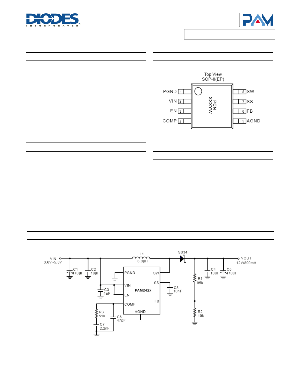
Typical Applications Circuit
Product Line o
Diodes Incorporated
PAM2421/ PAM2422/ PAM2423
3A, 4.5A, 5.5A PWM STEP-UP DC-DC CONVERTER
Pin Assignments
Applications
TFT LCD Monitors
Battery-Powered Equipment
Set-Top Boxes
DSL and Cable Modems and Routers
PAM2421/PAM2422/PAM2423
Document number: DSxxxxx Rev. 1 - 1
1 of 10
www.diodes.com
November 2012
© Diodes Incorporated
Page 2

A
f
Pin Descriptions
Pin
Number
1 PGND
2 IN
3 EN
4 COMP
5 AGND
6 FB
7 SS
8 SW
— Exposed PAD
SOP-8(EP)
Pin Name
Power Ground
Supply Input
Enable Control. Connect to a logic high level to enable the IC. Connect to a logic low
level to disable the IC. When unused, connect EN pin to IN (do not leave pin floating).
Error Amplifier Compensation Node
Analog Ground
Feedback Input.Connect this pin a resistor divider from the output to set the output
voltage. FB is regulated to 1.262V.
Soft Start Control Input. Connect a capacitor from this pin to Ground to set soft-start
timing duration. SS is discharged to ground in shutdown. SS may be left unconnected if
soft start is not desired.
Switch Output. Connect this pin to the inductor and the schottky diode. To minimize
EMI, minimize the PCB trace path between this pin and the input bypass capacitor.
Connected to Ground
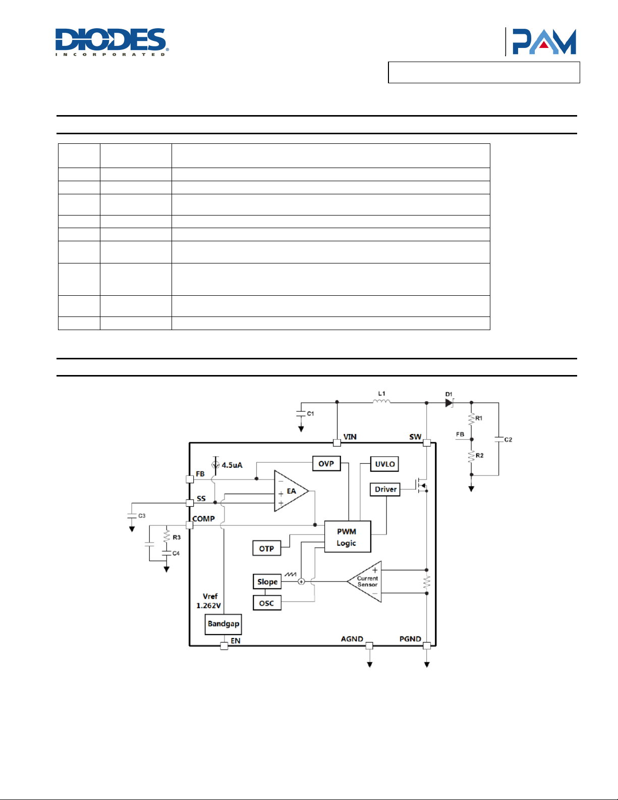
Functional Block Diagram
Product Line o
Diodes Incorporated
PAM2421/ PAM2422/ PAM2423
Function
PAM2421/PAM2422/PAM2423
Document number: DSxxxxx Rev. 1 - 1
2 of 10
www.diodes.com
November 2012
© Diodes Incorporated
Page 3

A
f
Product Line o
Diodes Incorporated
PAM2421/ PAM2422/ PAM2423
Absolute Maximum Ratings (@T
These are stress ratings only and functional operation is not implied. Exposure to absolute maximum ratings for prolonged time periods may
affect device reliability. All voltages are with respect to ground.
Parameter Rating Unit
SW to Ground -0.3 to +28 V
VIN, EN, FB, SS, COMP to Ground -0.3 to +6.5 V
Continuous SW Current Internally Limited V
Operating Temperature Range -40 to +150 °C
Storage Temperature Range -55 to +150 °C
Lead Temperature (Soldering, 10 sec) 300 °C
Recommended Operating Conditions (@T
Parameter Rating Unit
Junction Temperature Range -40 to +125
Ambient Temperature Range -40 to +85
= +25°C, unless otherwise specified.)
A
= +25°C, unless otherwise specified.)
A
°C
Thermal Information
Parameter Symbol Package Max Unit
Thermal Resistance (Junction to Case)
Thermal Resistance (Junction to Ambient)
θ
JC
θ
JA
PAM2421/PAM2422/PAM2423
Document number: DSxxxxx Rev. 1 - 1
SOP-8(EP) 75
SOP-8(EP) 180
3 of 10
www.diodes.com
°C/W
November 2012
© Diodes Incorporated
Page 4

A
f
Product Line o
Diodes Incorporated
PAM2421/ PAM2422/ PAM2423
Electrical Characteristics (@T
Parameter Test Conditions Min Typ Max Units
Input Voltage 2.7 5.5 V
Under Voltage Lockout Threshold
Under Voltage Lockout Hysteresis 200 mV
Quiscent Supply
Supply Current in Shutdown EN = Ground 0.1 1.0 µA
Switching Frequency 520 kHz
Maximum Duty Cycle 85 %
FB Feedback Voltage 1.237 1.262 1.287 V
FB Input Current 0 80 nA
FB Voltage Line Regulation
Switch Current Limit
Switching On Resisitance
Switch Leakage Current
Soft Start Pin Bias Current
Logic High Threshold EN Pin 1.4 V
Logic Low Threshold EN Pin 0.4 V
EN Pull Down Resistor 1 mΩ
Thermal Shutdown Temperature 160 °C
Thermal Shutdown Hystersis 40 °C
PAM2421/PAM2422/PAM2423
Document number: DSxxxxx Rev. 1 - 1
= +25°C, VIN = VEN = 5V, unless otherwise specified.)
A
V
Rising
IN
V
= 1.4V, Not Switching
FB
VFB = 1.0V, Switching
V
from 2.7V to 5.5V
FB
PAM2421
PAM2422 4.5
PAM2421 5.5
PAM2421 130
PAM2423 70
V
= 10V, EN = Ground
SW
V
= 1.2V
SS
V
= 3.2V
IN
Duty Cycle = 70%
4 of 10
www.diodes.com
2.5 V
0.25 0.35
3 5
0.05 0.15 %/V
3
15 µA
2.0 4.5 7.0 µA
mA
A
mΩ PAM2422 100
November 2012
© Diodes Incorporated
Page 5

A
f
Typical Operating Characteristics (@T
= +25°C, VIN = VEN = 5V, V
A
Product Line o
Diodes Incorporated
PAM2421/ PAM2422/ PAM2423
= 0V, unless otherwise specified.)
FREQ
PAM2421/PAM2422/PAM2423
Document number: DSxxxxx Rev. 1 - 1
5 of 10
www.diodes.com
November 2012
© Diodes Incorporated
Page 6

A
f
Typical Performance Characteristics (cont.) (@T
PAM2421/ PAM2422/ PAM2423
= +25°C, VIN = VEN = 5V, V
A
Product Line o
Diodes Incorporated
= 0V, unless otherwise specified.)
FREQ
PAM2421/PAM2422/PAM2423
Document number: DSxxxxx Rev. 1 - 1
6 of 10
www.diodes.com
November 2012
© Diodes Incorporated
Page 7

A
f
Product Line o
Diodes Incorporated
PAM2421/ PAM2422/ PAM2423
Application Information
The PAM242x are highly efficient step-up DC/DC converters that employ a current mode, fixed frequency pulse-width modulation (PWM)
architecture with excellent line and load regulation.The PAM242x operate at constant switching frequency under medium to high load current
conditions. At light loads, these devices operate in a pulse-skipping mode in order to improve light-load efficiency.
Soft-Start
The PAM242x both offer a programmable soft-start function which minimizes inrush current during startup. The soft-start period is programmed
by connecting a 10nF capacitor between SS and Ground. Operation of the soft-start function is as follows: when the IC is disabled, SS is actively
discharged to Ground. Upon enabling the IC, CSS is charged with a 4.5µA current so that the voltage at SS increases in a controlled manner.
The peak inductor current is limited by the voltage at SS, so that the input current is limited until the soft-start period expires, and the regulator
can achieve its full output current rating.
Setting the Output Voltage
The both feature external adjustable output voltages of up to 24V. To program the output voltage, simply connect a resistive voltage divider
between the output, FB, and GND, with resistors set according to the following equation:
FB
7 of 10
www.diodes.com
November 2012
© Diodes Incorporated
V
OUT
Where V
is 1.262V.
FB
x2R1R
1
V
Rectifier Selection
For optimal performance, the rectifier should be a Schottky rectifier that is rated to handle both the output voltage as well as the peak switch
current.
Open Voltage Protection
The features internal automatic over-voltage protection, when feedback voltage is higher than 115%.
Open Protection
Once the outputs achieve regulation, if the voltage at FB falls below 0.2V the controller will automatically disable, preventing the controller from
running open-loop and potentially damaging the IC and load.
Shutdown
Drive EN low to disable the IC and reduce the supply current to just 0.1µA. As with all nonsynchronous step-up DC/DC converters, the external
Schottky diode provides a DC path from the input to the output in shutdown. As a result, the output drops to one diode voltage drop below the
input in shutdown.
The PAM242x both feature integrated thermal overload protection. Both devices are automatically disabled when their junction temperatures
exceed +160°C, and automatically re-enable when the die temperature decreases by 40°C.
PAM2421/PAM2422/PAM2423
Document number: DSxxxxx Rev. 1 - 1
Page 8

A
f
Ordering Information
Product Line o
Diodes Incorporated
PAM2421/ PAM2422/ PAM2423
Part Number Peak Current Package Type Standard Package
PAM2421AECADJR 3A SOP-8(EP) 2500 Units/Tape & Reel
PAM2422AECADJR 4.5A SOP-8(EP) 2500 Units/Tape & Reel
PAM2423AECADJR 5.5A SOP-8(EP) 2500 Units/Tape & Reel
Marking Information
PAM2421/PAM2422/PAM2423
Document number: DSxxxxx Rev. 1 - 1
8 of 10
www.diodes.com
November 2012
© Diodes Incorporated
Page 9

A
f
Package Outline Dimensions (cont.) (All dimensions in mm.)
SOP-8(EP)
Product Line o
Diodes Incorporated
PAM2421/ PAM2422/ PAM2423
PAM2421/PAM2422/PAM2423
Document number: DSxxxxx Rev. 1 - 1
9 of 10
www.diodes.com
November 2012
© Diodes Incorporated
Page 10

A
f
Product Line o
Diodes Incorporated
PAM2421/ PAM2422/ PAM2423
DIODES INCORPORATED MAKES NO WARRANTY OF ANY KIND, EXPRESS OR IMPLIED, WITH REGARDS TO THIS DOCUMENT,
INCLUDING, BUT NOT LIMITED TO, THE IMPLIED WARRANTIES OF MERCHANTABILITY AND FITNESS FOR A PARTICULAR PURPOSE
(AND THEIR EQUIVALENTS UNDER THE LAWS OF ANY JURISDICTION).
Diodes Incorporated and its subsidiaries reserve the right to make modifications, enhancements, improvements, corrections or other changes
without further notice to this document and any product described herein. Diodes Incorporated does not assume any liability arising out of the
application or use of this document or any product described herein; neither does Diodes Incorporated convey any license under its patent or
trademark rights, nor the rights of others. Any Customer or user of this document or products described herein in such applications shall assume
all risks of such use and will agree to hold Diodes Incorporated and all the companies whose products are represented on Diodes Incorporated
website, harmless against all damages.
Diodes Incorporated does not warrant or accept any liability whatsoever in respect of any products purchased through unauthorized sales channel.
Should Customers purchase or use Diodes Incorporated products for any unintended or unauthorized application, Customers shall indemnify and
hold Diodes Incorporated and its representatives harmless against all claims, damages, expenses, and attorney fees arising out of, directly or
indirectly, any claim of personal injury or death associated with such unintended or unauthorized application.
Products described herein may be covered by one or more United States, international or foreign patents pending. Product names and markings
noted herein may also be covered by one or more United States, international or foreign trademarks.
Diodes Incorporated products are specifically not authorized for use as critical components in life support devices or systems without the express
written approval of the Chief Executive Officer of Diodes Incorporated. As used herein:
A. Life support devices or systems are devices or systems which:
1. are intended to implant into the body, or
2. support or sustain life and whose failure to perform when properly used in accordance with instructions for use provided in the
labeling can be reasonably expected to result in significant injury to the user.
B. A critical component is any component in a life support device or system whose failure to perform can be reasonably expected to cause the
failure of the life support device or to affect its safety or effectiveness.
Customers represent that they have all necessary expertise in the safety and regulatory ramifications of their life support devices or systems, and
acknowledge and agree that they are solely responsible for all legal, regulatory and safety-related requirements concerning their products and any
use of Diodes Incorporated products in such safety-critical, life support devices or systems, notwithstanding any devices- or systems-related
information or support that may be provided by Diodes Incorporated. Further, Customers must fully indemnify Diodes Incorporated and its
representatives against any damages arising out of the use of Diodes Incorporated products in such safety-critical, life support devices or systems.
Copyright © 2012, Diodes Incorporated
www.diodes.com
IMPORTANT NOTICE
LIFE SUPPORT
PAM2421/PAM2422/PAM2423
Document number: DSxxxxx Rev. 1 - 1
10 of 10
www.diodes.com
November 2012
© Diodes Incorporated
 Loading...