

Page 1
A
f
Description
The PAM2401 is a high efficiency, current mode, fixed frequency,
step-up DC/DC converter with true output disconnect and inrush
current limiting. The device includes one 0.10Ω N-channel MOSFET
switch and one 0.15Ω P-channel synchronous rectifier. This product
has the ability to simply program the output voltage from 2.5V to
5.0V.The switching frequency is 1.0MHz, programmable current limit
set by an external resistor from 1.0A to 3.0A with internal soft-start.
When loading became light, the converter will automatically enter into
PSM to improve the efficiency.
Quiescent current is only 150µA during Pulse Skip Mode operation,
maximizing battery life in portable applications. Other features include
: <1µA shutdown, anti-ringing control, Hiccup mode at short
protection, over voltage protection and over temperature protection.
The PAM2401 is available in MSOP-8 and U-DFN3030-12 packages
NEW PRODUCT
Diodes Incorporated
1.0MHz STEP-UP DC-DC CONVERTER
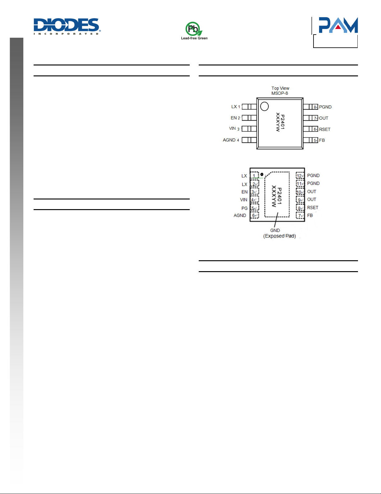
Pin Assignments
Product Line o
PAM2401
Features
• Up to 95% Efficiency
• True Output Disconnect
• Inrush Current Limiting When Power On
• Output Current up to 1000mA at V
• Fixed Frequency Operation Up to 1MHz
• 0.9V to 4.75V Input Range
• 2.5V to 5.0V Adjustable Output Voltage
• Guaranteed 1.0V Start-Up
• Programmable Current Limit
• Internal Soft-Start
• Internal Compensation
• Pulse Sipping Mode at Light Load Operation
• Hiccup Mode Short Protection
• Over Voltage Protection
• Over Temperature Protection
• <1µA Shutdown Current
• Power Good Indicator
• MSOP-8 and U-DFN3030-12 packages
• Totally Lead-Free & Fully RoHS Compliant (Notes 1 & 2)
• Halogen and Antimony Free. “Green” Device (Note 3)
Notes: 1. No purposely added lead. Fully EU Directive 2002/95/EC (RoHS) & 2011/65/EU (RoHS 2) compliant.
2. See http://www.diodes.com/quality/lead_free.html for more information about Diodes Incorporated’s definitions of Halogen- and Antimony-free, "Green"
and Lead-free.
3. Halogen- and Antimony-free "Green” products are defined as those which contain <900ppm bromine, <900ppm chlorine (<1500ppm total Br + Cl) and
<1000ppm antimony compounds.
= 3V and V
IN
PAM2401
Document number: DS37285 Rev. 1 - 2
OUT
= 5.0V
www.diodes.com
Applications
• Handheld Computers
• Cordless Phones
• GPS Receivers
• Battery Backup Supplies
1 of 10
May 2014
© Diodes Incorporated
Page 2
A
f
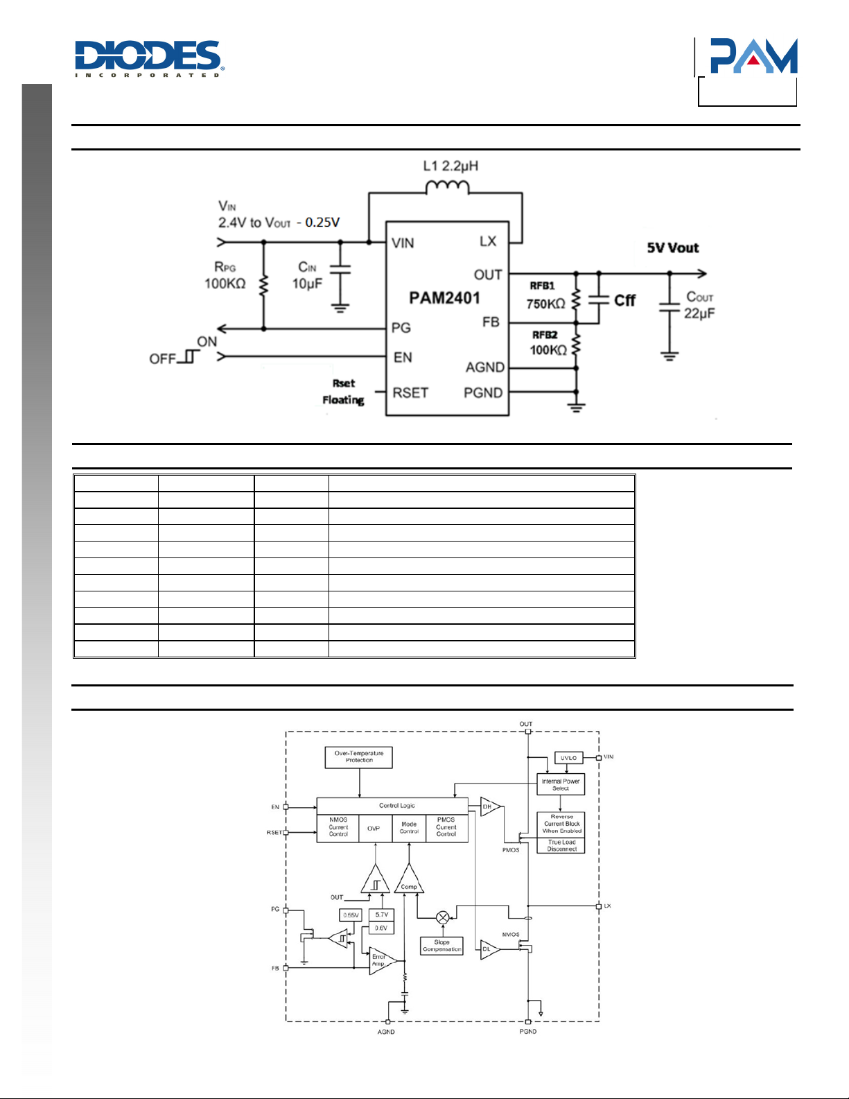
Typical Applications Circuit
Product Line o
Diodes Incorporated
PAM2401
NEW PRODUCT
Pin Descriptions
MSOP-8 U-DFN3030-12 Name Function
1 1,2 LX Switch Pin
2 3 EN Enables Control Input.
3 4 VIN Input Voltage Pin
-- 5 PG Power Good Indicator Pin, Open Drain Output
4 6 AGND Analog Ground
5 7 FB Feedback Pin Internally Set to 0.6V.
6 8 RSET Current Limit Setting
7 9,10 OUT Output Pin
8 11,12 PGND Power Ground
Exposed Pad EP Thermal Pad of the Package. Can Be Connected to PGND
Functional Block Diagram
PAM2401
Document number: DS37285 Rev. 1 - 2
2 of 10
www.diodes.com
May 2014
© Diodes Incorporated
Page 3
A
f
Product Line o
Diodes Incorporated
Absolute Maximum Ratings (@T
These are stress ratings only and functional operation is not implied. Exposure to absolute maximum ratings for prolonged time periods may
affect device reliability. All voltages are with respect to ground.
Parameter Rating Unit
Input Voltage -0.3 to +6.0 V
SW Voltage -0.3 to +6.0 V
SHDN, FB Voltage -0.3 to +6.0 V
V
OUT
Operating Temperature Range -40 to +85 °C
Storage Temperature Range -65 to +125 °C
Lead Temperature (Soldering, 10 sec) 300 °C
Recommended Operating Conditions (@T
Parameter Rating Unit
NEW PRODUCT
Ambient Temperature Range -40 to +85
Junction Temperature Range -40 to +125
= +25°C, unless otherwise specified.)
A
-0.3 to +6.0 V
= +25°C, unless otherwise specified.)
A
°C
Thermal Information
PAM2401
Parameter Package Symbol Max Unit
Thermal Resistance
(Junction to Case)
Thermal Resistance
(Junction to Ambient)
Internal Power Dissipation
PAM2401
Document number: DS37285 Rev. 1 - 2
MSOP-8
U-DFN3030-12 8.5
MSOP-8
U-DFN3030-12 60
MSOP-8
U-DFN3030-12 1.66
Θ
JC
Θ
JC
P
D
3 of 10
www.diodes.com
75
180
0.55
°C/W
W
May 2014
© Diodes Incorporated
Page 4

A
f
Electrical Characteristics (T
PARAMETER SYMBOL Test Conditions Min Typ Max Units
Input Voltage Range
Minimum Startup Voltage
Shutdown Supply Current
Quiescent Current Iq
Oscillator Frequency
Maximum Duty Cycle
Output-Voltage Adjust Range
FB Regulation Voltage
Load Regulation LDR
Line Regulation LNR
Drain-Source On-State Resistance
NEW PRODUCT
N-Channel Current Limit (Note)
Pre-charge Current I-Charge
Pre-charge Time T-Charge
SW Leakage Current ILSW 0.1 2 µA
Power Good Threshold VPG 92 %
EN Threshold High
EN Threshold Low
Over Temperature Threshold TOTSD 160 °C
Over Temperature Hysteresis THYS 50 °C
Note: N-Channel current limit is guaranteed by design.
= +25°C, V
A
V
R
= 3.3V, V
IN
V
IN
STARTUP
I
SD
f
OSC
D
MAX
V
O
V
FB
DS(ON)
I
LIMIT
VIN = 0.9V
V
H
OUT
No load, V
IO =1A , VO = 5V
IO = 0.1A, VO = 3.3V
0.1 1 µA
No load, switching (measured with
external feedback); V
0.8 1 1.2 MHz
87.5 %
2.5 5 V
No Load 0.588 0.6 0.612 V
I
= 1mA to 1000mA
OUT
V
= 2.5V to 4.75V, IO = 0.5A
O
P MOSFET 150 250 mΩ
N MOSFET 100 170 mΩ
R
Floating or R
SET
R
SET
R
= 66KΩ
SET
V
+0.5V < VIN
OUT
V
+0.5V < VIN
OUT
VH VIN = 3.3V
V
VIN > 1.2V
L
Product Line o
Diodes Incorporated
= 5V, L = 2.2µH, unless otherwise noted.)
= 5V
O
= 100KΩ
O
SET
= 5V
> 200KΩ
0.9 4.75 V
2.7 4.75
1 V
150 µA
2.5 %
0.3 %/V
3 A
1.5 A
1 A
500 mA
400 µs
0.8
1.5
0.2 V
PAM2401
V
PAM2401
Document number: DS37285 Rev. 1 - 2
4 of 10
www.diodes.com
May 2014
© Diodes Incorporated
Page 5

A
f
Product Line o
Diodes Incorporated
PAM2401
Application Information
Output Voltage Set Equation
The output voltage of the PAM2401, V
connected to the FB pin and the typical value of the voltage at the FB pin is 0.6V. The following equation is used to set the
V
: V
OUT
according to the equation, so a 750kΩ resistor should be chosen for R1.
= 0.6 (1+R1/R2) For example, if output voltage of 5V is needed, with a chosen R2 value of 100kΩ ,the value of R1 can be calculated
OUT
Inductor Selection
To select an inductor for use in PAM2401 applications, it is worth noting that the inductor current saturation rating should be larger than the
possible peak inductor current to ensure proper operation, and should have low DCR (DC resistance). Using an inductor the saturation current of
which is lower than required can cause a dramatic drop in the inductance and can decay the maximum output current levels severely. For most
applications, the value of the inductor should be in the range ofs 1µH to 4.7µH. Its value is chosen based on the desired ripple current.
Larger value inductors result in lower ripple currents, and smaller value inductors result in higher ripple currents. A 1.5µH or 2.2µH inductor will be
the best choice for most PAM2401 applications. The following equation can also help give a good approximate value for the inductor.
V
INxD
NEW PRODUCT
D Duty Cycle=1-V
(Ip).
=
L
Δ
ILxf
, F Switching Frequency = 1.0MHz, ∆IL Ripple Current in the Inductor, i.e., 20% to 40% of the maximum inductor current
IN/VOUT
Output and Input Capacitor Selection
Input Capacitor
At least a 10µF input capacitor is recommended to reduce the input ripple and switching noise for normal operating conditions, while a 10-22µF
capacitor may be required for higher power and dynamic loads. Larger values and lower ESR (Equivalent Series Resistance) may be needed if
the application require very low input ripple. It follows that ceramic capacitors are a good choice for applications. Note that the input capacitor
should be located as close as possible to the IC.
Output Capacitor
A minimum output capacitor value of 22µF is recommended and may be increase to a larger value. The ESR of the output capacitor is important
because it determines the peak to peak output voltage ripple by the following equation:
V
Δ 2
OUT
Multilayer ceramic capacitors are an excellent choice as they have extremely low ESR and are available in small footprints.
>>
Δ
xRESR
IL
PAM2401
Document number: DS37285 Rev. 1 - 2
, is set by an external resistor divider from VOUT to ground as shown in figure 1. The divider tap is
OUT
5 of 10
www.diodes.com
© Diodes Incorporated
May 2014
Page 6

A
f
Typical Performance Characteristics (T
Output Current (mA)
Output Current (mA)
NEW PRODUCT
100
95
90
85
80
75
70
Efficiency (%)
65
60
55
50
0 100 200 300 400 500 600 700 800 900 1000
Figure 4 Efficiency vs. Output Current (MSOP-8)
5.40
5.35
5.30
5.25
5.20
5.15
5.10
5.05
5.00
4.95
4.90
Output Voltage (V)
4.85
4.80
4.75
4.70
4.65
4.60
0 100 200 300 400 500 600 700 800 900 1000
Figure 6 Output Voltage vs. Output Current
Vin=3.3V
Vin=4.5V
Vin=3.3V
Vin=4.5V
= +25°C, V
A
= 3.3V, V
IN
Product Line o
Diodes Incorporated
PAM2401
= 5V, unless otherwise noted.)
OUT
100
95
90
85
80
75
70
Efficiency (%)
65
60
55
50
0 100 200 300 400 500 600 700 800 900 1000
Figure 5 Efficiency vs. Output Current (U-DFN)
2200
2000
1800
1600
1400
1200
1000
800
600
Maximun Output Current Ability (mA)
400
200
0
0.5 1.0 1.5 2.0 2.5 3.0 3.5 4.0 4.5
Figure 7 Maximum Output Current vs. Input Voltage
Output Current (mA)
test on steady state
Input Voltage (V)
Vin=3.3V
Vin=4.5V
Vout=3.3V
Vout=3.6V
Vout=4.2V
vout=5V
3.2
3.0
2.8
2.6
2.4
2.2
2.0
1.8
1.6
Inductor Current limit (A)
1.4
1.2
1.0
0.8
0.6
50 60 70 80 90 100 110 120 130 140 150 160 170 180 190
RSET Resistance (Kohm)
Vin=3.3V, Vo=5V
Figure 8 Inductor Current Limit vs. RSET Resistance
160
150
140
130
120
110
Dynamic Supply Current (uA)
100
90
-40-30-20-100 102030405060708090100110120
Figure 9 Dynamic Supply Current vs. Temperature
Vin=4.5V,Vo=5V,Io=0A
Temperature (oC)
PAM2401
Document number: DS37285 Rev. 1 - 2
6 of 10
www.diodes.com
May 2014
© Diodes Incorporated
Page 7

A
f
Typical Performance Characteristics (cont.) (T
2.6
Vo=3.3V
Vo=3.6V
2.4
Vo=4.2V
Vo=5V
2.2
2.0
1.8
1.6
1.4
1.2
Minimum startup input voltage(V)
1.0
0.8
0 100 200 300 400 500 600 700 800 900 1000 1100
Figure 10 Minimum Startup Input Voltage vs. Output Current
Output Current(mA)
= +25°C, V
A
= 3.3V, V
IN
OUT
Figure 11 Enable Turn On (I
(CH1: Enable; CH2: V
Product Line o
Diodes Incorporated
= 5V, unless otherwise noted.)
= 1A)
O
; CH3:SW; CH4: IO)
OUT
PAM2401
NEW PRODUCT
Figure 12 Enable Turn Off (I
(CH1: Enable; CH2:V
OUT
Figure 14 Output Ripple (I
(CH1: SW; CH2:V
= 1A)
O
; CH3:SW; CH4:Io)
= 0.2A)
O
; CH4:IL)
OUT-AC
Figure 13 Output Ripple (I
(CH1:SW; CH2: V
Figure 15 V
OUT
(CH2:V
OUT-AC
Short Protection (IO = 1A)
; CH3:IL)
OUT
= 0A)
O
; CH4:IL)
Figure 16 V
PAM2401
Document number: DS37285 Rev. 1 - 2
Short Recovery (IO = 1A)
OUT
(CH2: V
; CH3: IL )
OUT
7 of 10
www.diodes.com
May 2014
© Diodes Incorporated
Page 8

A
f
Ordering Information
Part Number Marking Package Type Standard Package
PAM2401SCADJ
PAM2401YPADJ
NEW PRODUCT
Marking Information
Package Type
S: MSOP-8
Y: U-DFN3030-12
P2401
XXXYW
P2401
XXXYW
PAM2401 X X XXX
Number of Pins
C: 8
P: 12
MSOP-8 2,500 units/ Tape & Reel
U-DFN3030-12 3,000 units/ Tape & Reel
Product Line o
Diodes Incorporated
PAM2401
Output Voltage
ADJ: ADJ
Top View
U-DFN3030-12
PAM2401
Document number: DS37285 Rev. 1 - 2
8 of 10
www.diodes.com
May 2014
© Diodes Incorporated
Page 9

A
f
Product Line o
Diodes Incorporated
PAM2401
Package Outline Dimensions (All dimensions in mm.)
Please see AP02002 at http://www.diodes.com/datasheets/ap02002.pdf for the latest version.
(1) MSOP-8
NEW PRODUCT
(2) U-DFN3030-12
y
A2
A1
D
4
x
1
0
x
1
0
°
Detail C
°
a
L
c
See Detail C
0.25
E
x
1
b
e
Gauge Plane
Seating Plane
4
E3
A3
A
E1
MSOP-8
Dim Min Max Typ
A - 1.10 A1 0.05 0.15 0.10
A2 0.75 0.95 0.86
A3 0.29 0.49 0.39
b 0.22 0.38 0.30
c 0.08 0.23 0.15
D 2.90 3.10 3.00
E 4.70 5.10 4.90
E1 2.90 3.10 3.00
E3 2.85 3.05 2.95
e - - 0.65
L 0.40 0.80 0.60
a 0° 8° 4°
x - - 0.750
y - - 0.750
All Dimensions in mm
Pin#1 ID
A
A1
D
D2
E2
E
e
b
A3
SEATING PLANE
L
U-DFN3030-12
Dim Min Max Typ
A 0.57 0.63 0.60
A1 0 0.05 0.02
A3
⎯ ⎯
b 0.18 0.28 0.23
D 2.90 3.10 3.00
D2 2.30 2.50 2.40
e
⎯ ⎯
E 2.90 3.10 3.00
E2 1.50 1.70 1.60
L 0.25 0.55 0.40
All Dimensions in mm
0.15
0.45
Suggested Pad Layout
Please see AP02001 at http://www.diodes.com/datasheets/ap02001.pdf for the latest version.
(1) MSOP-8
PAM2401
Document number: DS37285 Rev. 1 - 2
Y1
X C
Y
www.diodes.com
9 of 10
Dimensions Value (in mm)
C 0.650
X 0.450
Y 1.350
Y1 5.300
May 2014
© Diodes Incorporated
Page 10

A
f
Product Line o
Diodes Incorporated
PAM2401
Suggested Pad Layout (cont.)
Please see AP02001 at http://www.diodes.com/datasheets/ap02001.pdf for the latest version.
(2) U-DFN3030-12
DIODES INCORPORATED MAKES NO WARRANTY OF ANY KIND, EXPRESS OR IMPLIED, WITH REGARDS TO THIS DOCUMENT,
NEW PRODUCT
INCLUDING, BUT NOT LIMITED TO, THE IMPLIED WARRANTIES OF MERCHANTABILITY AND FITNESS FOR A PARTICULAR PURPOSE
(AND THEIR EQUIVALENTS UNDER THE LAWS OF ANY JURISDICTION).
Diodes Incorporated and its subsidiaries reserve the right to make modifications, enhancements, improvements, corrections or other changes
without further notice to this document and any product described herein. Diodes Incorporated does not assume any liability arising out of the
application or use of this document or any product described herein; neither does Diodes Incorporated convey any license under its patent or
trademark rights, nor the rights of others. Any Customer or user of this document or products described herein in such applications shall assume
all risks of such use and will agree to hold Diodes Incorporated and all the companies whose products are represented on Diodes Incorporated
website, harmless against all damages.
Diodes Incorporated does not warrant or accept any liability whatsoever in respect of any products purchased through unauthorized sales channel.
Should Customers purchase or use Diodes Incorporated products for any unintended or unauthorized application, Customers shall indemnify and
hold Diodes Incorporated and its representatives harmless against all claims, damages, expenses, and attorney fees arising out of, directly or
indirectly, any claim of personal injury or death associated with such unintended or unauthorized application.
Products described herein may be covered by one or more United States, international or foreign patents pending. Product names and markings
noted herein may also be covered by one or more United States, international or foreign trademarks.
This document is written in English but may be translated into multiple languages for reference. Only the English version of this document is the
final and determinative format released by Diodes Incorporated.
Diodes Incorporated products are specifically not authorized for use as critical components in life support devices or systems without the express
written approval of the Chief Executive Officer of Diodes Incorporated. As used herein:
A. Life support devices or systems are devices or systems which:
1. are intended to implant into the body, or
labeling can be reasonably expected to result in significant injury to the user.
B. A critical component is any component in a life support device or system whose failure to perform can be reasonably expected to cause the
failure of the life support device or to affect its safety or effectiveness.
Customers represent that they have all necessary expertise in the safety and regulatory ramifications of their life support devices or systems, and
acknowledge and agree that they are solely responsible for all legal, regulatory and safety-related requirements concerning their products and any
use of Diodes Incorporated products in such safety-critical, life support devices or systems, notwithstanding any devices- or systems-related
information or support that may be provided by Diodes Incorporated. Further, Customers must fully indemnify Diodes Incorporated and its
representatives against any damages arising out of the use of Diodes Incorporated products in such safety-critical, life support devices or systems.
Copyright © 2014, Diodes Incorporated
www.diodes.com
2. support or sustain life and whose failure to perform when properly used in accordance with instructions for use provided in the
X
CY
X1
G
G
Z
IMPORTANT NOTICE
LIFE SUPPORT
Dimensions Value (in mm)
Z 2.60
G 0.15
X 1.80
X1 0.60
Y 0.28
C 0.45
PAM2401
Document number: DS37285 Rev. 1 - 2
10 of 10
www.diodes.com
May 2014
© Diodes Incorporated
 Loading...