

Page 1
A
f
Product Line o
Diodes Incorporated
PAM2321
3MHz, FAST TRANSIENT 2A STEP-DOWN CONVERTER
Description
The PAM2321 is a 2A step-down converter with a typical input
voltage of 3.3V and a fixed output voltage of 1.2V or an adjustable
output. The 3MHz switching frequency enables the use of small
external components. The ultra-small 3mmx3mm footprint and high
efficiency make the PAM2321 an ideal choice for portable
applications.
The PAM2321 delivers 2A maximum output current while consuming
only 55µA no-load quiescent current. Low R
MOSFETs and 100% duty cycle operation make the PAM2321 the
ideal choice for high output voltage, high current applications which
require a low dropout threshold.
The PAM2321 provides excellent transient response and output
accuracy across the operating range.
The PAM2321 maintains high efficiency throughout the load range.
The PAM2321 automatically optimizes efficiency during light load
mode (PSM) and maintains constant frequency and low output ripple
during PWM mode.
Over-temperature and short circuit protection safeguard the PAM2321
and system components from damage.
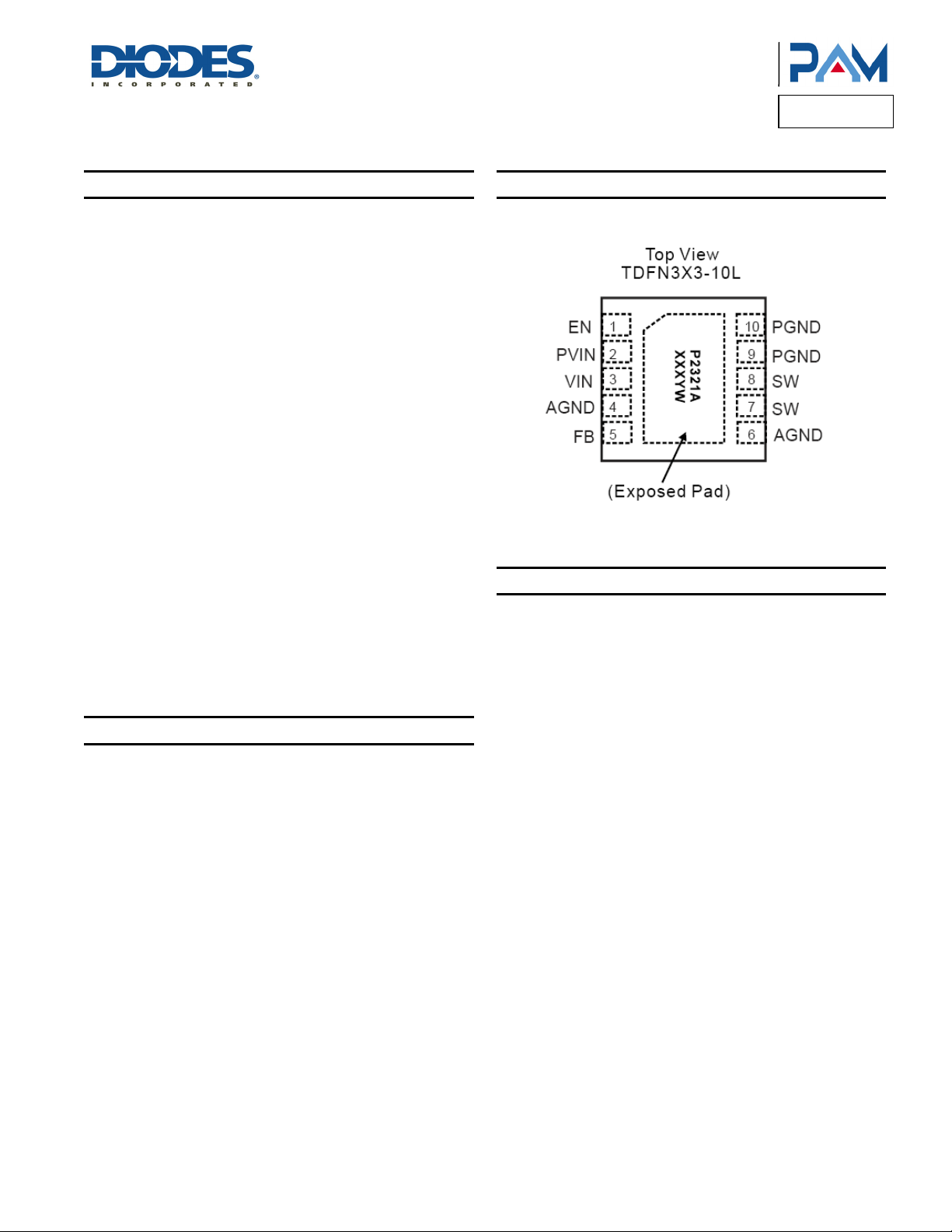
The PAM2321 are available in Pb-free, ultrasmall, low profile,
TDFN3X3-10 package. The product is rated over a temperature range
of -40°C to +85°C.
DS(ON)
integrated
Features
• 2A Maximum Output Current
• Tiny 0.47µH Chip Inductor
• Excellent Transient Response
• Input Voltage: 2.7V to 5.5V
• Fixed or Adjustable Output Voltage Options:
Fixed Output Voltage: 1.2V
Adjustable Output Voltage: 1.0V to V
• High Efficiency with 3MHz Switching Frequency
• 55µA No Load Quiescent Current
• 100% Duty Cycle Low-Dropout Operation
• Internal Soft-Start
• Over-Temperature and Current Limit Protection
• <1µA Shutdown Current
• -40°C to +85°C Temperature Range
• Pb-Free/Halogen Free Package
IN
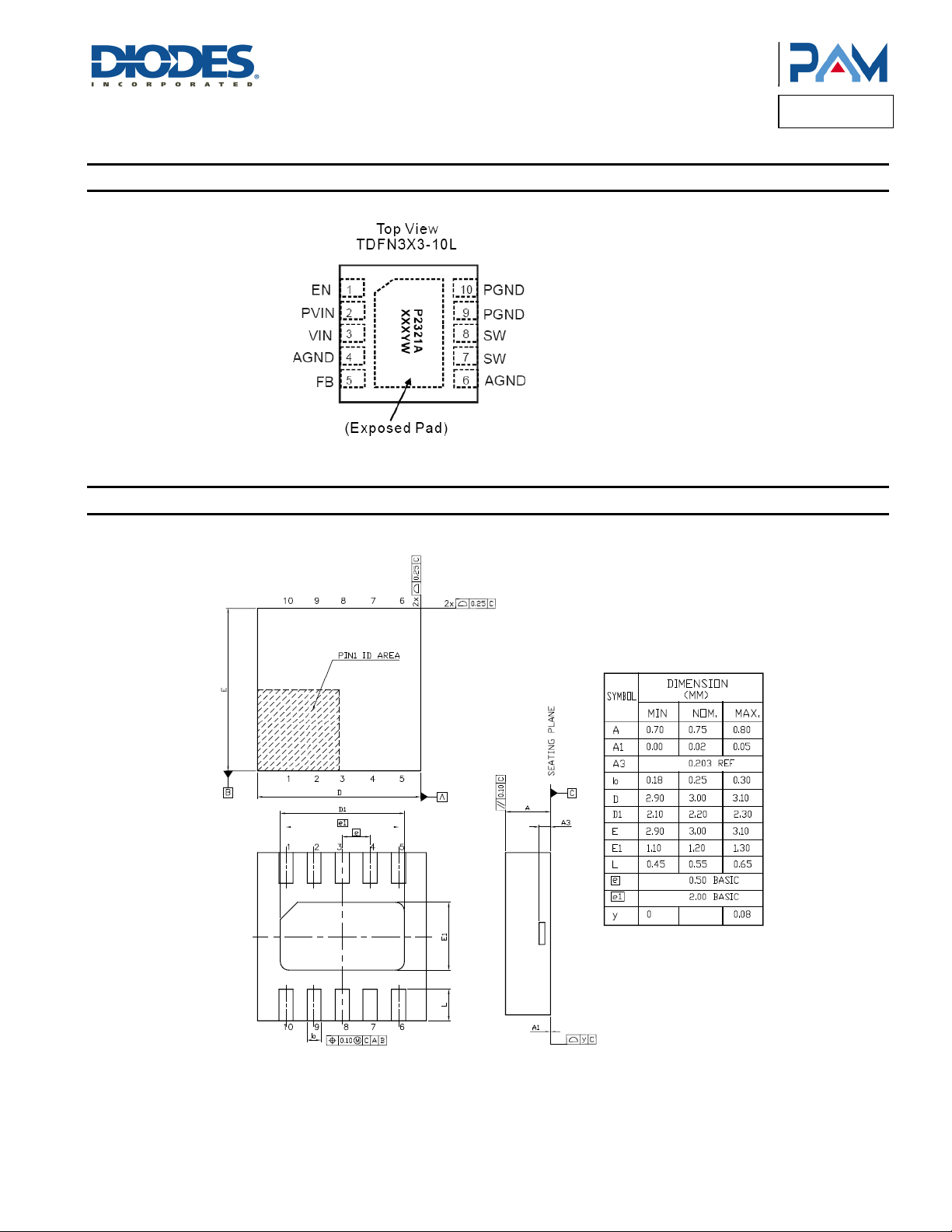
Pin Assignments
Applications
• Cellular Phone
• Digital Cameras
• Hard Disk Drives
• MP3 Players
• PDAs and Handheld Computers
• Portable Media Players
• USB Devices
• Wireless Network Cards
• RoHS/REACH Compliant
PAM2321
Document number: DSxxxxx Rev. 2 - 1
1 of 11
www.diodes.com
January 2013
© Diodes Incorporated
Page 2
A
f
(
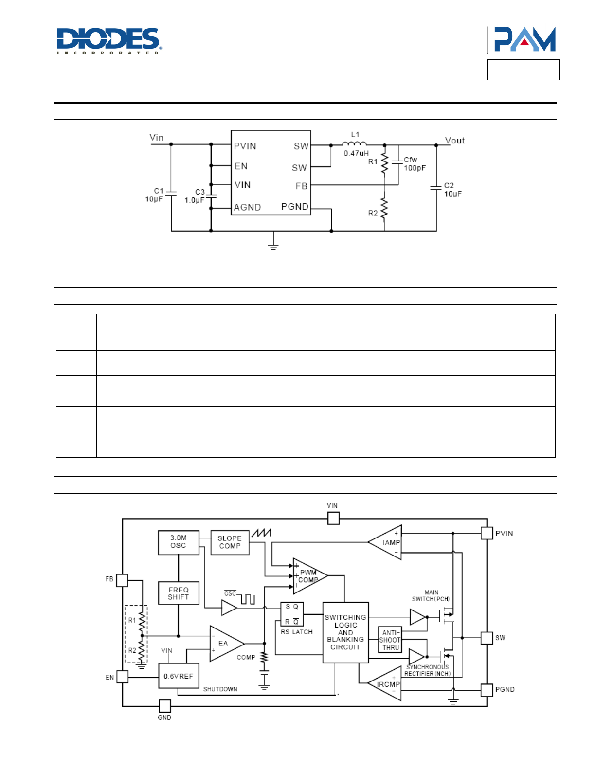
Typical Applications Circuit
Product Line o
Diodes Incorporated
PAM2321
Pin Descriptions
Pin
Name
PGND
PVIN
AGND
Main power ground return pin. Connect to the output and input capacitor return.
Input power supply tied to the source of the high side P-Channel MOSFET.
Power supply; supplies power for the internal circuitry.
VIN
Feedback input pin. This pin is connected directly to the converter output for the 1.2V fixed output version, or connected to an
FB
external resistor divider for the adjustable output version.
Analog ground. This pin is internally connected to the analog ground of the control circuitry.
Enable pin. A logic low disables the converter and it consumes less than 1μA of current. When connected high, it resumes normal
EN
operation.
Switching node. Connect the inductor to this pin. It is internally connected to the drain of both high and low side MOSFETs.
SW
Exposed pad of the package provides both electrical contact to the ground and good thermal
EP
contact to the PCB. This pad must be soldered to the PCB for proper operation.
Functional Block Diagram
V
OUT
+=
Function
)
2R/1R1*6.0
PAM2321
Document number: DSxxxxx Rev. 2 - 1
2 of 11
www.diodes.com
January 2013
© Diodes Incorporated
Page 3
A
f
Product Line o
Diodes Incorporated
PAM2321
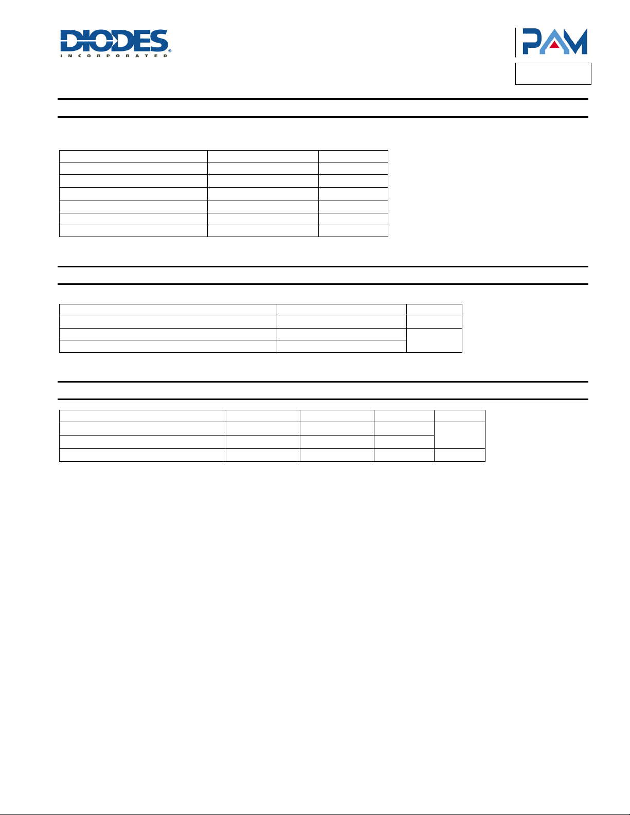
Absolute Maximum Ratings (@T
These are stress ratings only and functional operation is not implied. Exposure to absolute maximum ratings for prolonged time periods may
affect device reliability. All voltages are with respect to ground.
Parameter Rating Unit
Input Voltage -0.3 to +6.5 V
EN, FB Pin Voltage
SW Pin Voltage
Junction Temperature 150 °C
Storage Temperature Range -65 to +150 °C
Soldering Temperature 300, 5sec °C
Recommended Operating Conditions (@T
Parameter Rating Unit
Supply Voltage 2.5 to 5.5 V
Operation Temperature Range -40 to +85
Junction Temperature Range -40 to +125
= +25°C, unless otherwise specified.)
A
-0.3 to V
-0.3 to (V
+0.3)
IN
IN
= +25°C, unless otherwise specified.)
A
V
V
°C
Thermal Information
Parameter Symbol Package Max Unit
Thermal Resistance (Junction to Case)
Thermal Resistance (Junction to Ambient)
Internal Power Dissipation
θ
JC
θ
JA
P
D
TDFN3x3-10 8.5
TDFN3x3-10 60
TDFN3x3-10 1.66 W
°C/W
PAM2321
Document number: DSxxxxx Rev. 2 - 1
3 of 11
www.diodes.com
January 2013
© Diodes Incorporated
Page 4
A
f
Product Line o
Diodes Incorporated
PAM2321
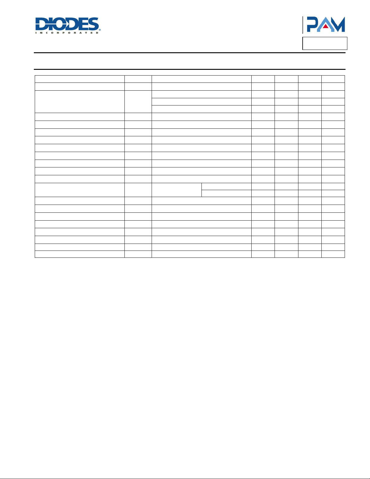
Electrical Characteristics
(@TA = +25°C, VIN = 3.3V, V
Parameter Symbol Test Conditions Min Typ Max Units
Input Voltage Range
UVLO Threshold
Output Voltage Range
Output Voltage Accuracy
Regulated Feedback Voltage
PMOS Current Limit
Output Voltage Line Regulation LNR
Output Voltage Load Regulation LDR
Quiescent Current
Shutdown Current
Oscillator Frequency
Drain-Source On-State Resisitance
SW Leakage Current
Start-Up Time
PSM Threshold
EN Threshold High
EN Threshold Low
EN Leakage Current
Over Temperature Protection OTP 150 °C
OTP Hysteresis OTH 30 °C
PAM2321
Document number: DSxxxxx Rev. 2 - 1
= 1.2V, CIN = 10µF, CO = 10µF, L = 0.47µH, unless otherwise specified.)
OUT
IN
Rising
V
IN
Hysteresis 250 mV
V
V
UVLO
VIN Falling
V
V
f
R
DS(ON)
I
OUT
OUT
V
I
LIM
I
I
SD
OSC
LSW
t
I
TH
V
V
I
EN
IO = 0mA
No Load 0.588 0.600 0.612 V
FB
V
= 3.3V to 4V
IN
I
= 1mA to 2A
O
No Load 55 90 µA
Q
VEN = 0V
IDS = 100mA
1 µA
VIN = 3.3V, VO = 1.2V
S
200 mA
1.4 V
EH
0.4 V
EL
±0.01 µA
P MOSFET 130 mΩ
N MOSFET 90 mΩ
4 of 11
www.diodes.com
2.7 3.3 5.5 V
2.6 2.7 V
2 V
1 1.2
VIN
V
-3.0 +3.0 %
3.0 A
0.3 %/V
1 %/A
1 µA
3 MHz
200 µs
January 2013
© Diodes Incorporated
Page 5
A
f
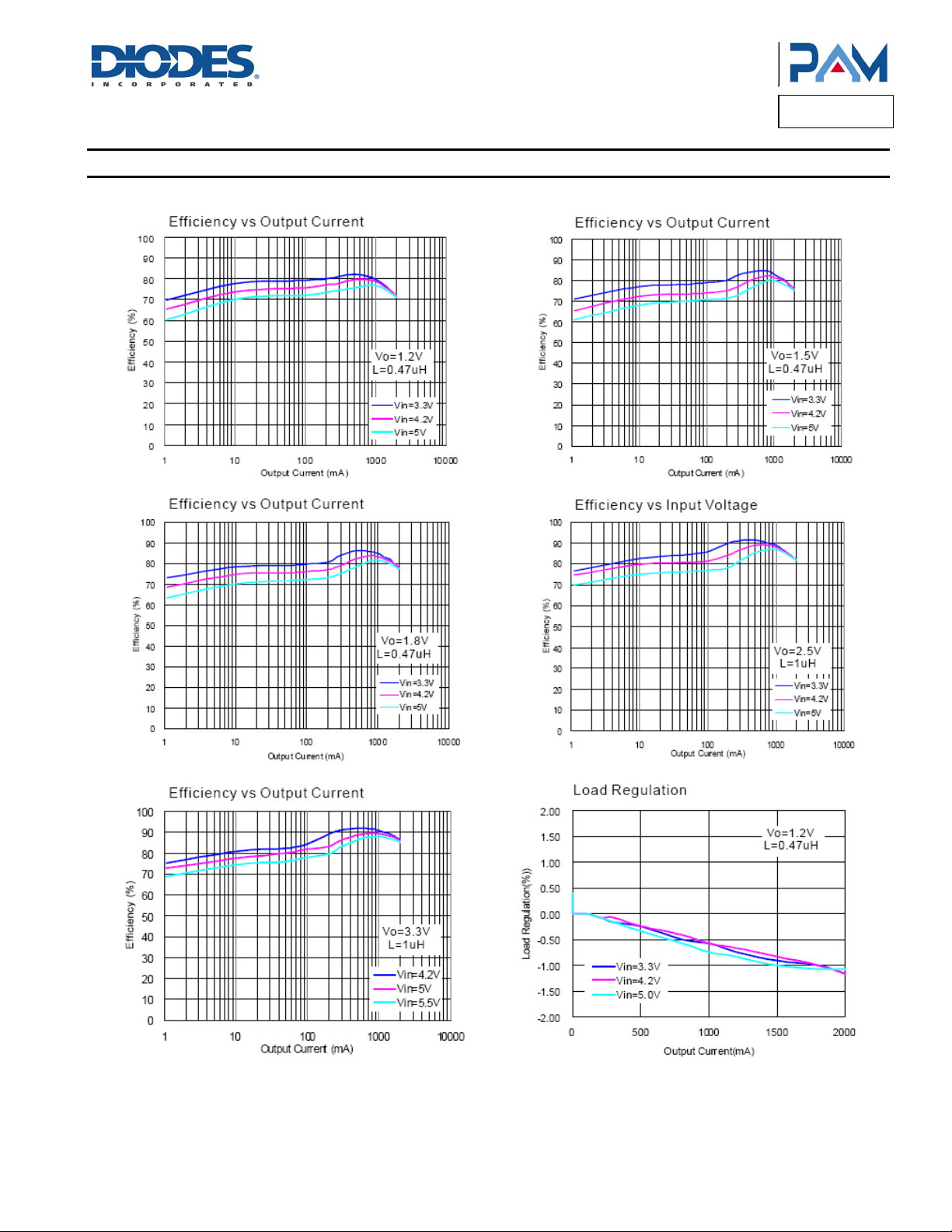
Typical Performance Characteristics (@T
Product Line o
Diodes Incorporated
PAM2321
= +25°C, CIN = 10µF, CO = 10µF, L = 0.47µH unless otherwise specified.)
A
PAM2321
Document number: DSxxxxx Rev. 2 - 1
5 of 11
www.diodes.com
January 2013
© Diodes Incorporated
Page 6
A
f
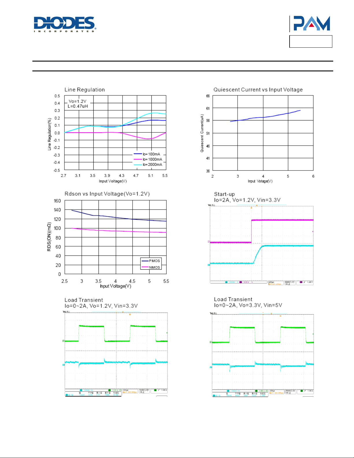
Typical Performance Characteristics (cont.) (@T
Product Line o
Diodes Incorporated
PAM2321
= +25°C, CIN = 10µF, CO = 10µF, L = 0.47µH unless otherwise specified.)
A
PAM2321
Document number: DSxxxxx Rev. 2 - 1
6 of 11
www.diodes.com
January 2013
© Diodes Incorporated
Page 7

A
f
Product Line o
Diodes Incorporated
PAM2321
Application Information
The basic PAM2321 application circuit is shown in Page 2. External component selection is determined by the load requirement, selecting L first
and then C
and C
IN
Inductor Selection
For most applications, the value of the inductor will fall in the range of 1μH to 4.7μH. Its value is chosen based on the desired ripple current and
efficiency. Large value inductors lower ripple current and small value inductors result in higher ripple currents. Higher V
the ripple current as shown in equation 3.0. A reasonable starting point for setting ripple current is ΔI
The DC current rating of the inductor should be at least equal to the maximum load current plus half the ripple current to prevent core saturation.
Thus, a 2.8A rated inductor should be enough for most applications (2A + 800mA). For better efficiency, choose a low DC-resistance inductor.
CIN and C
In continuous mode, the source current of the top MOSFET is a square wave of duty cycle V
ESR input capacitor sized for the maximum RMS current must be used. The maximum RMS capacitor current is given by:
This formula has a maximum at V
significant deviations do not offer much relief. Note that the capacitor manufacturer's ripple current ratings are often based on 2000 hours of life.
This makes it advisable to further derate the capacitor, or choose a capacitor rated at a higher temperature than required. Consult the
manufacturer if there is any question.
The selection of C
Typically, once the ESR requirement for C
output ripple ΔV
Δ
OUT
C
Δ
I
IN
.
OUT
1
()()
Lf
⎛
⎜
−=
1
V
OUTL
⎜
⎝
⎞
V
OUT
⎟
Equation (1)
⎟
V
IN
⎠
Selection
[]
()
−
required
OUT
is determined by:
OUT
≈
Δ
≅
II
OMAXRMS
= 2V
IN
OUT
is driven by the required effective series resistance (ESR).
OUT
⎛
⎜
+
ESR
IV
LOUT
⎜
⎝
⎞
1
⎟
⎟
fC8
OUT
⎠
VVV
V
IN
, where I
RMS
has been met, the RMS current rating generally far exceeds the I
2/1
OUTINOUT
= I
/2. This simple worst-case condition is commonly used for design because even
OUT
or V
IN
OUT
= 800mA (40% of 2A).
L
. To prevent large voltage transients, a low
OUT/VIN
(P-P) requirement. The
RIPPLE
also increases
Where f = operating frequency, C
highest at maximum input voltage since ΔI
= output capacitance and ΔIL = ripple current in the inductor. For a fixed output voltage, the output ripple is
OUT
increases with input voltage.
L
Using Ceramic Input and Output Capacitors
Higher values, lower cost ceramic capacitors are now becoming available in smaller case sizes. Their high ripple current, high voltage rating and
low ESR make them ideal for switching regulator applications. Using ceramic capacitors can achieve very low output ripple and small circuit size.
When choosing the input and output ceramic capacitors, choose the X5R or X7R dielectric formul ations. These dielectrics have the best
temperature and voltage characteristics of all the ceramics for a given value and size.
Thermal Consideration
Thermal protection limits power dissipation in the PAM2321. When the junction temperature exceeds +150°C, the OTP (Over Temperature
Protection) starts the thermal shutdown and turns the pass transistor off. The pass transistor resumes operation after the junction temperature
drops below +120°C.
For continuous operation, the junction temperature should be maintained below +125°C. The power dissipation is defined as:
()
−+
2
I
is the step-down converter quiescent current. The term tsw is used to estimate the full load step-down converter switching losses.
Q
=
IP
OD
V
IN
RVVRV
PAM2321
Document number: DSxxxxx Rev. 2 - 1
L)ON(DSOINH)ON(DSO
()
t
SW
++
VIIF
INQOS
7 of 11
www.diodes.com
January 2013
© Diodes Incorporated
Page 8

A
f
Product Line o
Diodes Incorporated
Application Information (cont.)
For the condition where the step-down converter is in dropout at 100% duty cycle, the total device dissipation reduces to:
2
OD
+=
VIRIP
INQH)ON(DS
PAM2321
Since R
voltage range. The maximum power dissipation depends on the thermal resistance of IC package, PCB layout, the rate of surrounding airflow
and temperature difference between junction and ambient. The maximum power dissipation can be calculated by the following formula:
Where T
junction to the ambient. Based on the standard JEDEC for a two layers thermal test board, the thermal resistance θ
60°C/W. The maximum power dissipation at T
P
, quiescent current, and switching losses all vary with input voltage, the total losses should be investigated over the complete input
DS(ON)
−
TT
=
P
D
is the maximum allowable junction temperature +125°C. TA is the ambient temperature and θJA is the thermal resistance from the
J(MAX)
= (125°C - 25°C) /60°C/W = 1.66W
D
A)MAX(J
θ
JA
of TDFN3x3 package is
JA
= +25°C can be calculated by following formula:
A
Setting the Output Voltage
The internal reference is 0.6V (Typical). The output voltage is calculated as below:
The output voltage is given by Table 1.
1R
Table 1: Resistor selection for output voltage setting.
V
O
V
O
1.2V 100k 100k
1.5V 150k 100k
1.8V 200k 100k
2.5V 380k 120k
3.3V 540k 120k
⎛
⎜
⎝
⎞
+=
1x6.0
⎟
2R
⎠
R1 R2
Pulse Skipping Mode (PSM) Description
When load current decreases, the peak switch current in Power-PMOS will be lower than skip current threshold and the device will enter into
Pulse Skipping Mode.
In this mode, the device has two states, working state and idle state. First, the device enters into working state control led by internal error
amplifier.When the feedback voltage gets higher than internal reference voltage, the device will enter into low I
blocks disabled. The output voltage will be reduced by loading or leakage current. When the feedback voltage gets lower than the internal
reference voltage, the convertor will start a working state again.
idle state with most of internal
Q
100% Duty Cycle Operation
As the input voltage approaches the output voltage, the converter turns the P-Channel transistor continuously on. In this mode the output voltage
is equal to the input voltage minus the voltage drop across the P-Channel transistor:
where R
= P-Channel switch ON resistance, I
DS(ON)
()
+−=
RRIVV
LDSONLOADINOUT
= Output Current, RL = Inductor DC Resistance
LOAD
UVLO and Soft-Start
The reference and the circuit remain reset until the VIN crosses its UVLO threshold. The PAM2321 has an internal soft-start circuit that limits the
in-rush current during start-up. This prevents possible voltage drops of the input voltage and eliminates the output voltage overshoot.
PAM2321
Document number: DSxxxxx Rev. 2 - 1
8 of 11
www.diodes.com
January 2013
© Diodes Incorporated
Page 9
A
f
Product Line o
Diodes Incorporated
PAM2321
Application Information (cont.)
Short Circuit Protection
When the converter output is shorted or the device is overloaded, each high-side MOSFET current-limit event (3A typ) turns off the high-side
MOSFET and turns on the low-side MOSFET. An internal counter is used to count the each current-limit event. The counter is reset after
consecutive high-side MOSFETs turn on without reaching current limit. If the current-limit condition persists, the counter fills up. The control logic
then stops both high-side and lowside MOSFETs and waits for a hiccup period, before attemping a new soft-start sequence. The counter bits is
decided by V
1.7%. The hiccup mode is disable during soft-start time.
voltage. If ≤VFB 0 2, the counter is 3-bit counter; if VFB >0.2 the counter is 6-bit counter. The typical hicuup made duty cycle is
FB
Thermal Shutdown
When the die temperature exceeds +150°C, a reset occurs and the reset remains until the temperature decrease to +120°C, at which time the
circuit can be restarted.
PCB Layout Check List
When laying out the printed circuit board, the following checklist should be used to ensure proper operation of the PAM2321. Check the following
in your layout:
1. The input capacitor should be close to IC as close as possible.
2. Must put a small decoupling capacitor between VIN PIN and AGND Pin.
3. Minimize the switching loop area to avoid excessive switching noise.
4. AGND and PGND should connect at input capacitor GND.
5. For the good thermal dissipation, PAM2321 has a heat dissipate pad in the bottom side, it should be soldered to PCB surface. For the copper
area can't be large in the component side, so we can use mu ltiple vias connect to other side of the PCB.
Ordering Information
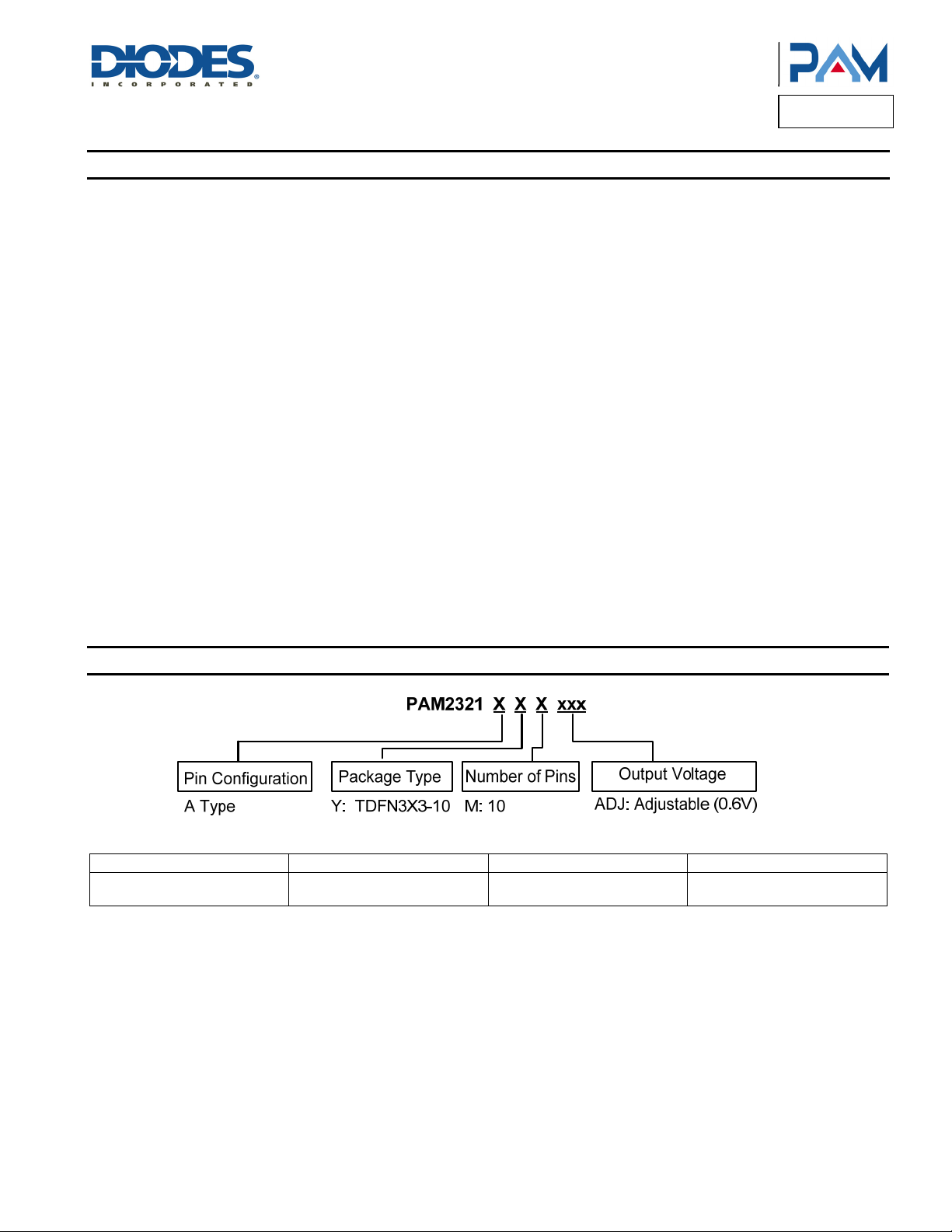
Part Number Output Voltage Part Type Standard Package
PAM2321AYMADJ
PAM2321
Document number: DSxxxxx Rev. 2 - 1
P2321A
XXXYW
T-DFN3x3-10 3000 Units/Tape & Reel
9 of 11
www.diodes.com
January 2013
© Diodes Incorporated
Page 10
A
f
Marking Information
Package Outline Dimensions (All dimensions in mm.)
TDFN3x3-10
Product Line o
Diodes Incorporated
PAM2321
A/B : Pin Configuration
X : Internal Code
Y : Year
W : Week
PAM2321
Document number: DSxxxxx Rev. 2 - 1
10 of 11
www.diodes.com
January 2013
© Diodes Incorporated
Page 11

A
f
Product Line o
Diodes Incorporated
PAM2321
DIODES INCORPORATED MAKES NO WARRANTY OF ANY KIND, EXPRESS OR IMPLIED, WITH REGARDS TO THIS DOCUMENT,
INCLUDING, BUT NOT LIMITED TO, THE IMPLIED WARRANTIES OF MERCHANTABILITY AND FITNESS FOR A PARTICULAR PURPOSE
(AND THEIR EQUIVALENTS UNDER THE LAWS OF ANY JURISDICTION).
Diodes Incorporated and its subsidiaries reserve the right to make modifications, enhancements, improvements, corrections or other changes
without further notice to this document and any product described herein. Diodes Incorporated does not assume any liability arising out of the
application or use of this document or any product described herein; neither does Diodes Incorporated convey any license under its patent or
trademark rights, nor the rights of others. Any Customer or user of this document or products described herein in such applications shall assume
all risks of such use and will agree to hold Diodes Incorporated and all the companies whose products are represented on Diodes Incorporated
website, harmless against all damages.
Diodes Incorporated does not warrant or accept any liability whatsoever in respect of any products purchased through unauthorized sales channel.
Should Customers purchase or use Diodes Incorporated products for any unintended or unauthorized application, Customers shall indemnify and
hold Diodes Incorporated and its representatives harmless against all claims, damages, expenses, and attorney fees arising out of, directly or
indirectly, any claim of personal injury or death associated with such unintended or unauthorized application.
Products described herein may be covered by one or more United States, international or foreign patents pending. Product names and markings
noted herein may also be covered by one or more United States, international or foreign trademarks.
This document is written in English but may be translated into multiple languages for reference. Only the English version of this document is the
final and determinative format released by Diodes Incorporated.
Diodes Incorporated products are specifically not authorized for use as critical components in life support devices or systems without the express
written approval of the Chief Executive Officer of Diodes Incorporated. As used herein:
A. Life support devices or systems are devices or systems which:
1. are intended to implant into the body, or
2. support or sustain life and whose failure to perform when properly used in accordance with instructions for use provided in the
labeling can be reasonably expected to result in significant injury to the user.
B. A critical component is any component in a life support device or system whose failure to perform can be reasonably expected to cause the
failure of the life support device or to affect its safety or effectiveness.
Customers represent that they have all necessary expertise in the safety and regulatory ramifications of their life support devices or systems, and
acknowledge and agree that they are solely responsible for all legal, regulatory and safety-related requirements concerning their products and any
use of Diodes Incorporated products in such safety-critical, life support devices or systems, notwithstanding any devices- or systems-related
information or support that may be provided by Diodes Incorporated. Further, Customers must fully indemnify Diodes Incorporated and its
representatives against any damages arising out of the use of Diodes Incorporated products in such safety-critical, life support devices or systems.
Copyright © 2013, Diodes Incorporated
www.diodes.com
IMPORTANT NOTICE
LIFE SUPPORT
PAM2321
Document number: DSxxxxx Rev. 2 - 1
11 of 11
www.diodes.com
January 2013
© Diodes Incorporated
 Loading...