Diodes AP7331 User Manual

300mA, LOW QUIESCENT CURRENT, FAST TRANSIENT
Description
The AP7331 is a 300mA, adjustable and fixed output
voltage, low dropout linear regulator. The device included
pass element, error amplifier, band-gap, current limit and
thermal shutdown circuitry. The device is turned on when EN
pin is set to logic high level.
The characteristics of low dropout voltage and low quiescent
current make it suitable for low power applications, for
example, battery powered devices. The typical quiescent
current is approximately 65μA.
Built-in current-limit and thermal-shutdown functions prevent
IC from damage in fault conditions.
The AP7331 is available in SOT25 and DFN2020-6
packages.
AP7331
LOW DROPOUT LINEAR REGULATOR
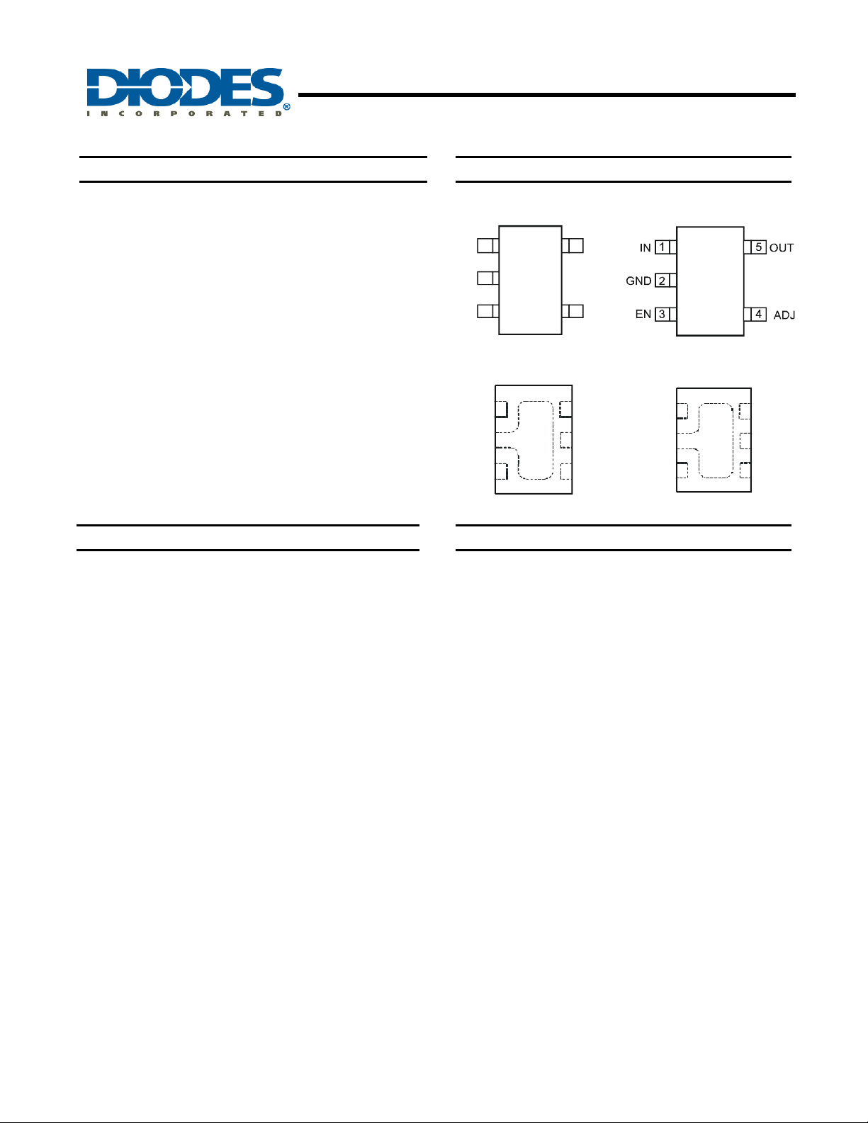
Pin Assignments
OUT
NC
SOT25 (ADJ Output)
(Top View)
DFN2020-6 (ADJ Output)
(To p Vie w)
1
EN
GND
2
3
IN
SOT25 (Fixed Output)
(To p Vie w)
IN
GND
EN
1
2
3
5
4
DFN2020-6 (Fixed Output)
(To p Vie w)
EN
GND
1
2
3
6
NC
5
NC
OUT
4IN
6
ADJ
5
NC
OUT
4
Features
• 300mA Low Dropout Regulator with EN
• Very low I
• Wide input voltage range: 2V to 6V
• Wide adjustable output: 0.8V to 5.0V
• Fixed output options: 1.0V to 3.3V
• PSRR: 65dB typical at 100Hz
• Fast start-up time: 80µs
• Stable with low ESR, 1µF ceramic output capacitor
• Excellent Load/Line Transient Response
• Low dropout: 300mV typical at 300mA
• Current limit protection
• Short circuit protection
• Thermal shutdown protection
• Ambient temperature range: -40ºC to 85°C
• SOT25 and DFN2020-6: Available in “Green” Molding
over full load: 65µA
Q
Applications
• XDSL Routers
• Wireless LAN Cards
• Desktop and Notebook Computers
• Battery Powered Equipments
Compound (No Br, Sb)
• Lead Free Finish/RoHS Compliant (Note 1)
Notes: 1. EU Directive 2002/95/EC (RoHS). All applicable RoHS exemptions applied. Please visit our website at http://www.diodes.com/products/lead_free.html
AP7331
Document number: DS31914 Rev. 3 - 2
1 of 13
www.diodes.com
January 2011
© Diodes Incorporated

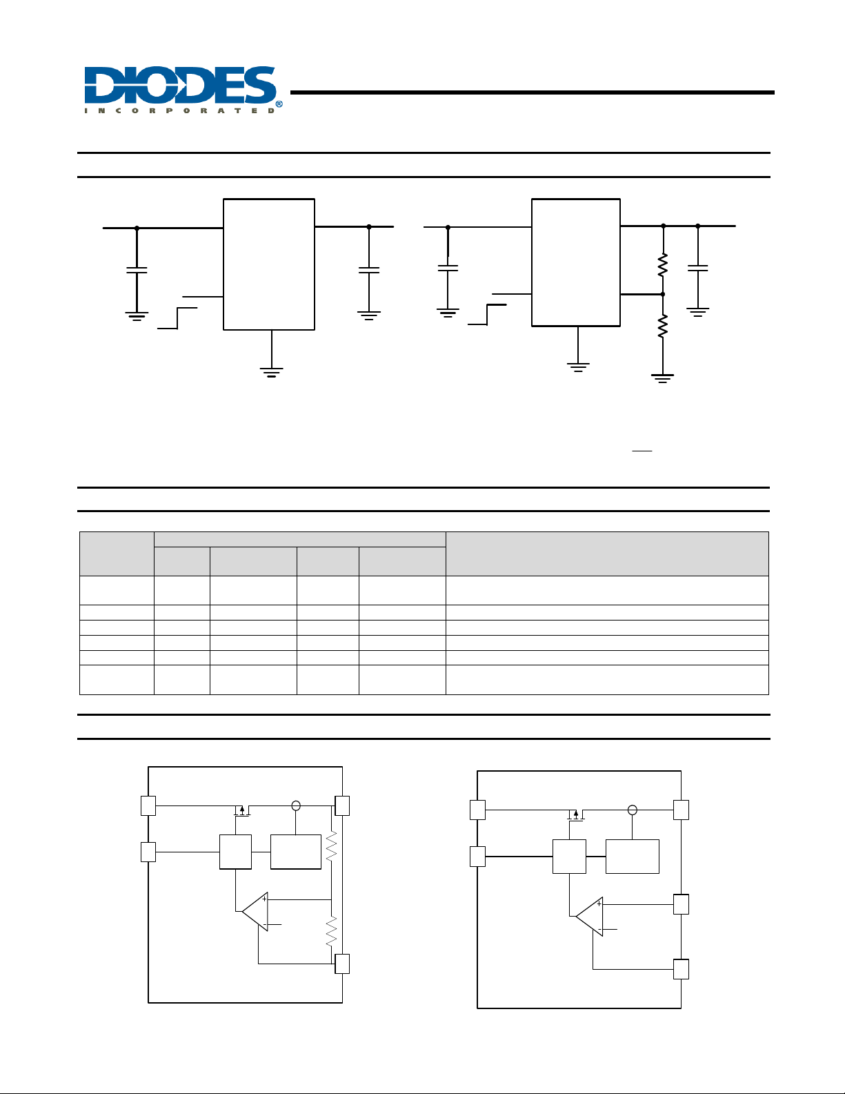
Typical Application Circuit
V
IN
IN
OUT
AP7331
300mA, LOW QUIESCENT CURRENT, FAST TRANSIENT
LOW DROPOUT LINEAR REGULATOR
V
V
OUT
IN
IN
OUT
V
OUT
AP7331
1uF
Enable
EN
GND
Fixed Output
1uF
1uF
Enable
Pin Descriptions
Pin Number
Pin Name
IN 1 3 1 3
SOT25
(fixed)
DFN2020-6
(fixed)
SOT25
(adj)
DFN2020-6
(adj)
Voltage input pin. Bypass to ground through at least
1µF capacitor
GND 2 2 2 2 Ground
EN 3 1 3 1 Enable input, active high
ADJ - - 4 6 Output feedback pin
NC 4 5, 6 - 5 No connection
OUT 5 4 5 4
Voltage output pin. Bypass to ground through 1µF
ceramic capacitor
Functional Block Diagram
AP7331
EN
ADJ
GND
Adjustable Output
⎛
⎜
1
V
OUT
V
REF
⎜
⎝
Description
R1
R2
⎞
R
1
⎟
+=
⎟
R
2
⎠
1uF
IN
EN
Gate
Driver
Fixed Version
AP7331
Document number: DS31914 Rev. 3 - 2
Current Limit
and Thermal
Shutdown
0.4V
OUT
R
R
GND
EN
IN
Gate
Driver
Adjustable V e rs ion
Current Limit
and Thermal
Shutdown
0.4V
OUT
ADJ
GND
2 of 13
www.diodes.com
January 2011
© Diodes Incorporated

AP7331
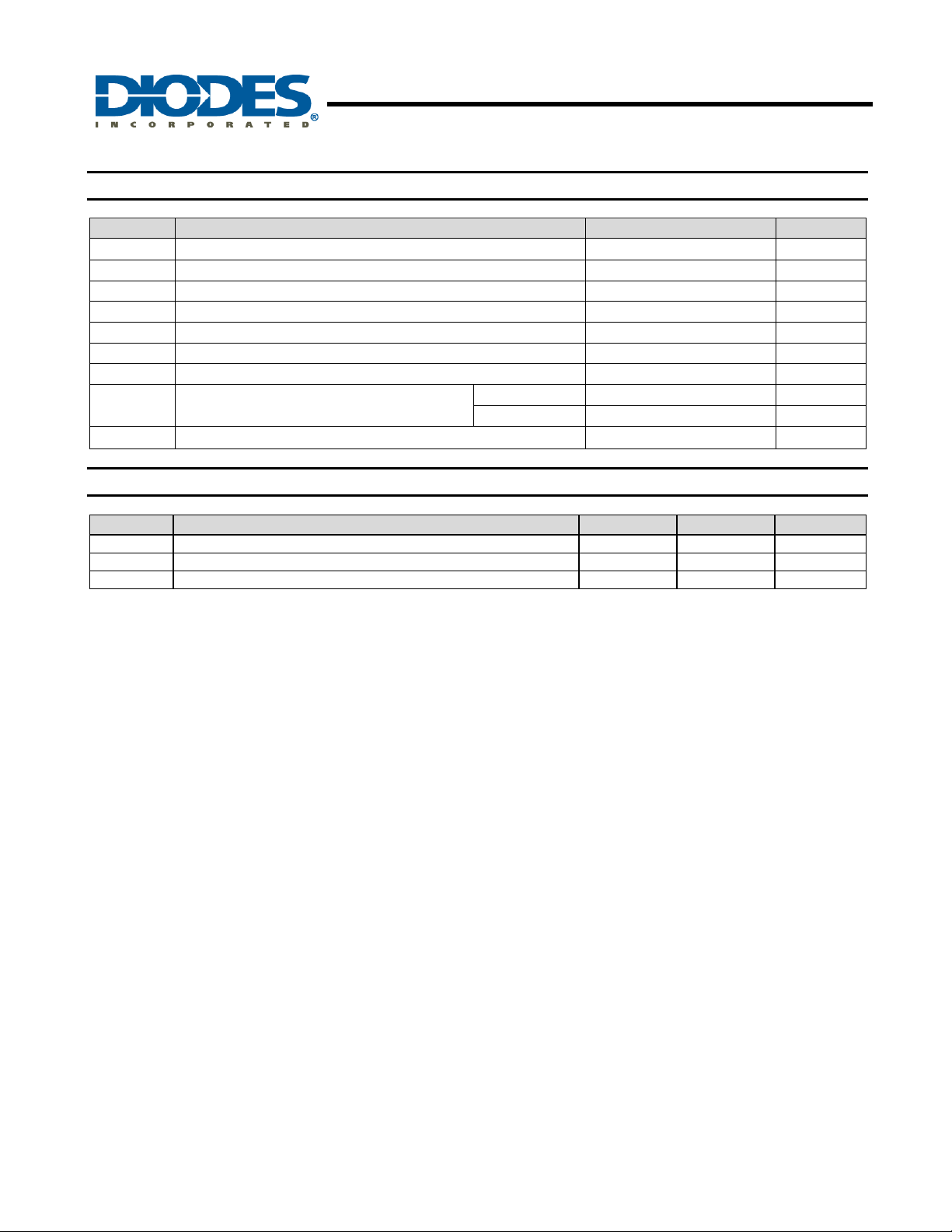
Absolute Maximum Ratings
Symbol Parameter Ratings Units
ESD HBM Human Body Model ESD Protection 6 kV
ESD MM Machine Model ESD Protection 400 V
VIN Input Voltage 7 V
EN Voltage VIN + 0.3 V
Continuous Load Current Internal Limited
TOP Operating Junction Temperature Range -40 ~ 125 °C
TST Storage Temperature Range -65 ~150 °C
PD Power Dissipation (Note 2)
TJ Maximum Junction Temperature 150 °C
Recommended Operating Conditions
Symbol Parameter Min Max Unit
V
IN
I
OUT
T
A
Notes: 2. Ratings apply to ambient temperature at 25°C
3. The device maintains a stable, regulated output voltage without a load current.
Input voltage 2 6 V
Output Current (Note 3) 0 300 mA
Operating Ambient Temperature -40 85
300mA, LOW QUIESCENT CURRENT, FAST TRANSIENT
LOW DROPOUT LINEAR REGULATOR
SOT25 640 mW
DFN2020-6 740 mW
°C
AP7331
Document number: DS31914 Rev. 3 - 2
3 of 13
www.diodes.com
January 2011
© Diodes Incorporated

AP7331
⎯
⎯
⎯
⎯
x
x
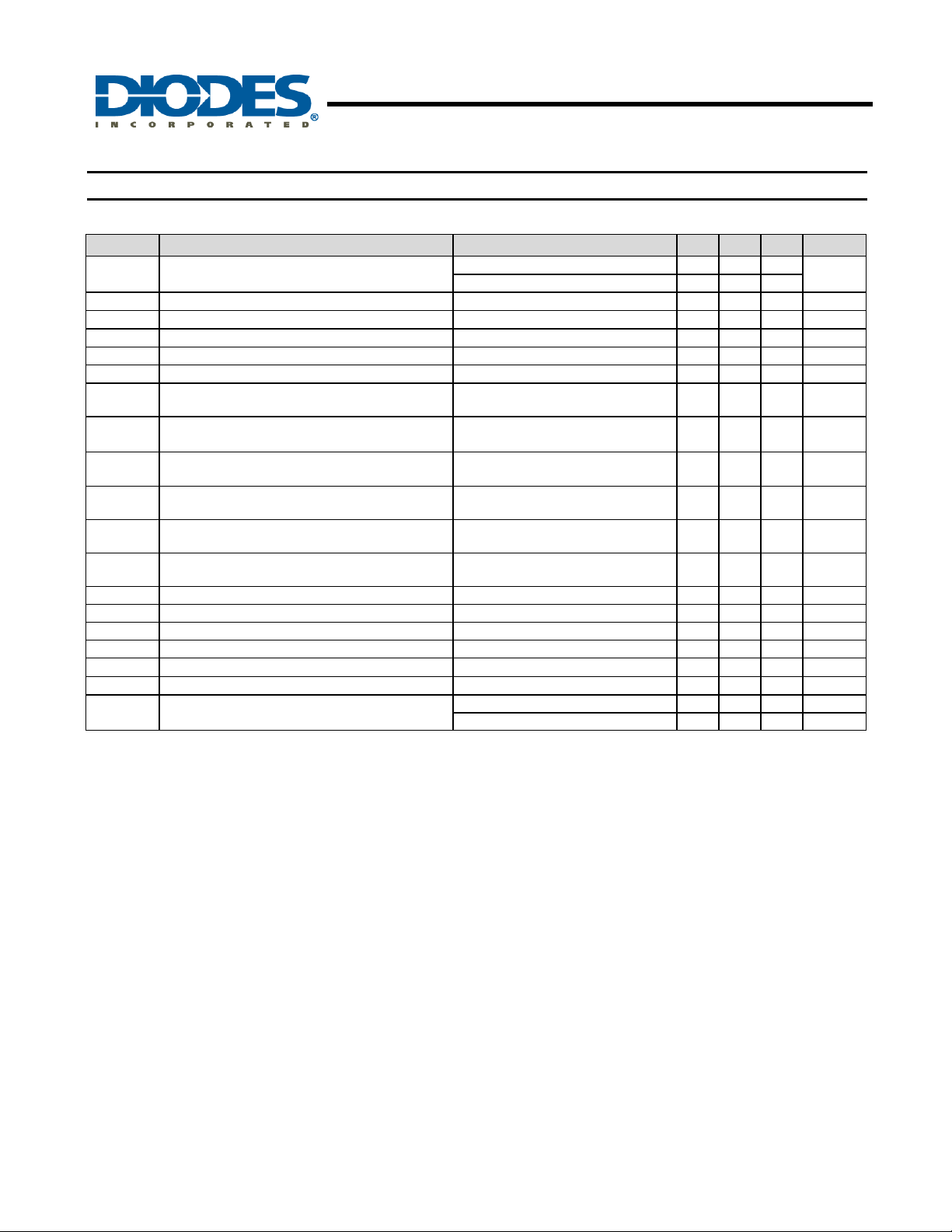
Electrical Characteristics
(TA = 25oC, V
Symbol Parameter Test Conditions Min Typ. Max Unit
I
Q
I
SHDN
I
LEAK
V
Dropout
V
REF
I
ADJ
V
OUT
ΔV
OUT
ΔV
/V
/
IN
ΔV
OUT
/V
OUT
tST Start-up Time
PSRR PSRR
I
SHORT
I
LIMIT
V
IL
V
IH
I
EN
T
SHDN
T
HYS
θ
Thermal Resistance Junction-to-Ambient
JA
Notes: 4. Dropout voltage is the voltage difference between the input and the output at which the output voltage drops 2% below its nominal value.
This parameter only applies to output voltages above 1.8V.
5. Test conditions for SOT25: Device mounted on FR-4 substrate PCB, with minimum recommended pad layout, 2oz copper, single sided
6. Test conditions for DFN2020-6: Device mounted on FR-4 substrate PCB, with minimum recommended pad layout, 2oz copper, double sided,
bottom layer is a copper plane.
= V
OUT
+1V, C
IN
= 1uF, C
IN
Input Quiescent Current
Input Shutdown Current VEN = 0V, I
Input Leakage Current VEN = 0V, OUT grounded
Dropout Voltage (Note 4) I
ADJ Reference Voltage (Adjustable version) I
ADJ Leakage (Adjustable version)
Output Voltage Accuracy
Line Regulation
Load Regulation
Short-circuit Current
Current Limit V
EN Input Logic Low Voltage VIN = V
EN Input Logic High Voltage VIN = V
EN Input Current VIN = 0V or V
Thermal Shutdown Threshold 140
Thermal Shutdown Hysteresis 15
300mA, LOW QUIESCENT CURRENT, FAST TRANSIENT
LOW DROPOUT LINEAR REGULATOR
OUT
= 1uF, V
= 2V, unless otherwise stated)
EN
= VIN, I
V
EN
V
= VIN, I
EN
= 300mA 300 550 mV
OUT
= 0mA 0.4 V
OUT
T
= -40oC to 85oC,
A
= 30mA
I
OUT
V
= (V
IN
= VIN, I
V
EN
V
= (V
IN
from 1mA to 300mA
I
OUT
= 0V to 2.0V, V
V
EN
= 300mA
I
OUT
V
= [V
IN
f = 100Hz, I
= V
V
IN
< 0.2V
V
OUT
OUT/ROUT
= 0mA
OUT
= 300mA 65 85
OUT
= 0mA
OUT
+1V) to V
OUT
= 1mA
OUT
+1V) to V
OUT
+1V]VDC + 0.5V
OUT
=30mA
OUT
to V
IN-Min
IN-Max
OUT
IN-Max
IN-Max
= 1V,
,
,
,
ppAC
-0.6 0.6 %
,
= 1A 400 600 mA
IN-Min
IN-Min
to V
to V
IN-Ma
0.4 V
IN-Ma
1.4 V
IN-Max
-1 1 μA
SOT25 (Note 5) 190
DFN2020-6 (Note 6) 167
55 75
1
1
1 μA
-2 2 %
0.01 0.20 %/V
80 μs
65 dB
100 mA
μA
μA
μA
°C
°C
o
C/W
o
C/W
AP7331
Document number: DS31914 Rev. 3 - 2
4 of 13
www.diodes.com
January 2011
© Diodes Incorporated
 Loading...