

Page 1
AP7217D
1.2V 600mA CMOS LDO
Features
• Low Current Consumption: Typ. 40μA
• Output Voltage: 1.2V
• Guaranteed 600mA Output Current
• Dropout Voltage 850mV at 600mA Output Current
• Input Voltage Range: 2.5V to 5.5V
• Current Limit Protection
• Thermal shutdown Protection
• Stability with Low ESR Capacitors
• Low Temperature Coeff icient
• SOT89-3L: Available in “Green” Molding Compound
(No Br, Sb)
• Lead Free Finish/ RoHS Compliant (Note 1)
Applications
• CD and MP3 Players
• Cellular and PCS Phones
• Digital Still Camera
• Hand-Held Computers
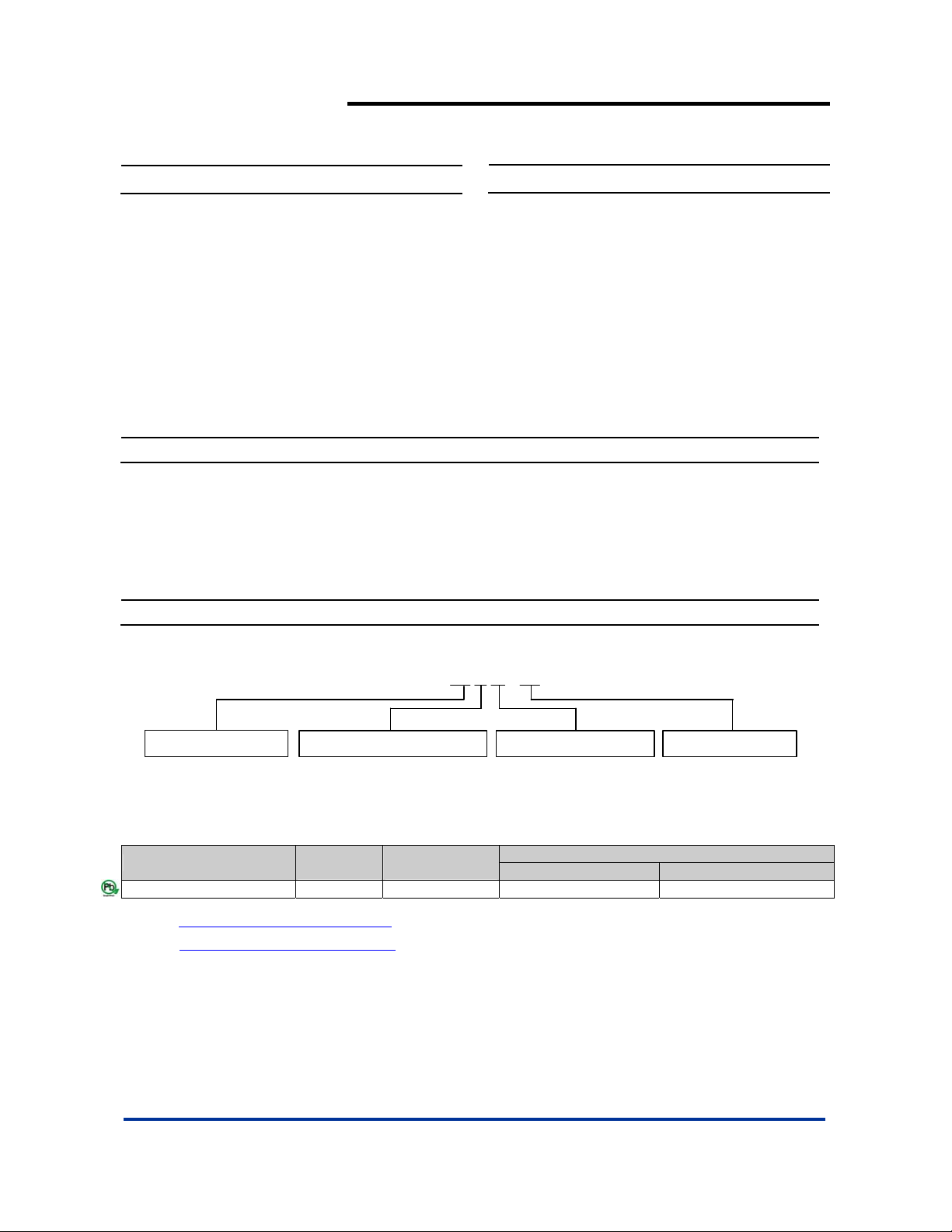
Ordering Information
AP 7217D - 12 Y G - 13
General Description
The AP7217D low-dropout linear regulator operates from 2.5V to
5.5V supply and delivers a guaranteed 600mA continuous load
current.
The space-saving SOT89-3L package is suitable f or “po cket” and
hand-held application.
Output voltage
12 : 1.2V
Package
Y : SOT89-3L
G : Green
PackingGreen
13 : Tape & Reel
Device
Package
Code
Packaging
(Note 2)
Quantity Part Number Suffix
13” Tape and Reel
AP7217D-12YG-13 Y SOT89-3L 2500/Tape & Reel -13
Notes: 1. EU Directive 2002/95/EC (RoHS). All applicable RoHS exemptions applied. Please visit our website at
http://www.diodes.com/products/lead_free.html
2. Pad layout as shown on Diodes Inc. suggested pad layout document AP02001, which can be found on our website at
http://www.diodes.com/datasheets/ap02001.pdf
.
.
AP7217D Rev. 2 1 of 9 FEBRUARY 2009
www.diodes.com © Diodes Incorporated
Page 2
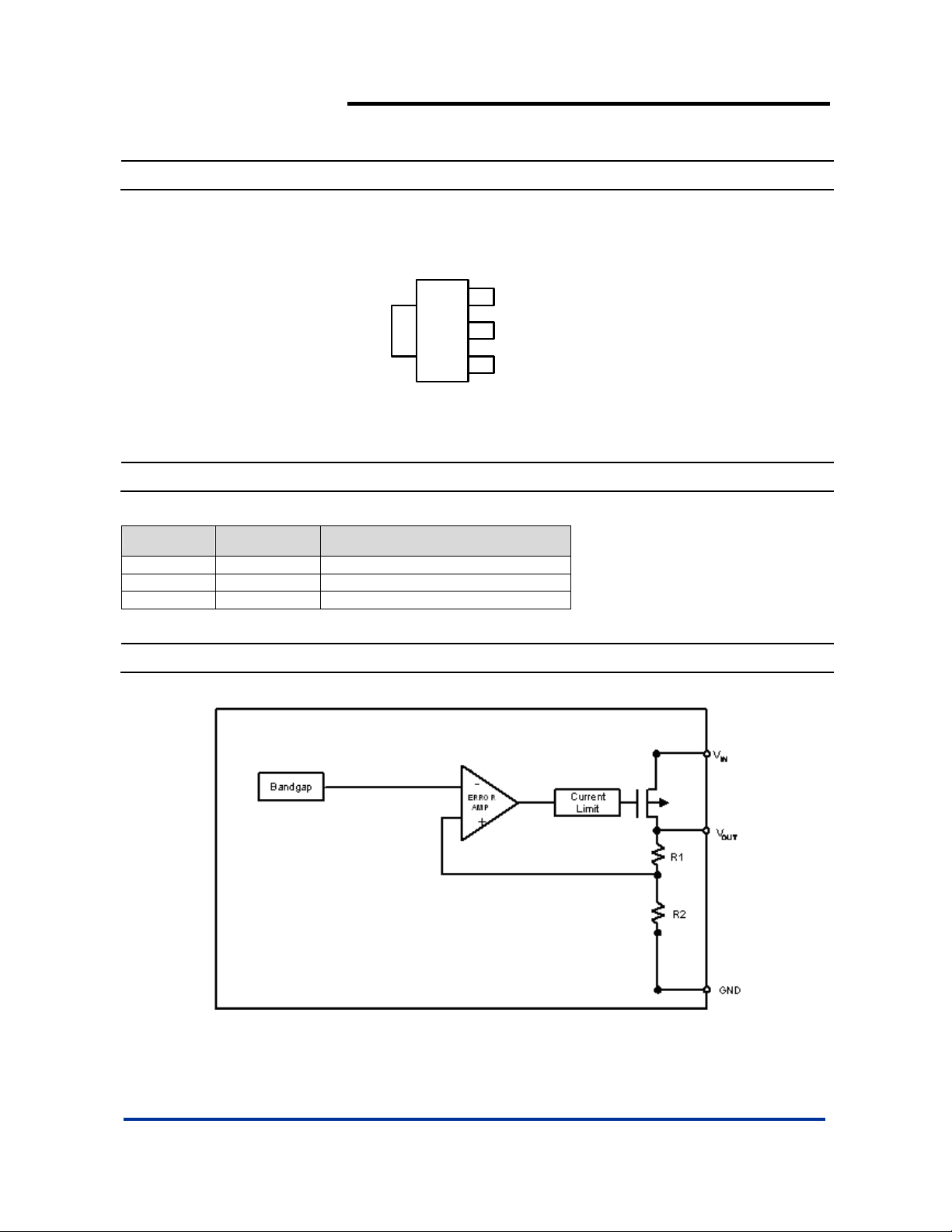
Pin Assignments
(1) SOT89-3L
AP7217D
1.2V 600mA CMOS LDO
( Top View )
Tab is V
Pin Descriptions
Pin Name Pin No. Function
GND 1 Ground
VIN 2 Supply Voltage
V
3 Voltage Output
OUT
Block Diagram
3
2
1
V
OUT
V
IN
GND
IN
AP7217D Rev. 2 2 of 9 FEBRUARY 2009
www.diodes.com © Diodes Incorporated
Page 3
AP7217D
1.2V 600mA CMOS LDO
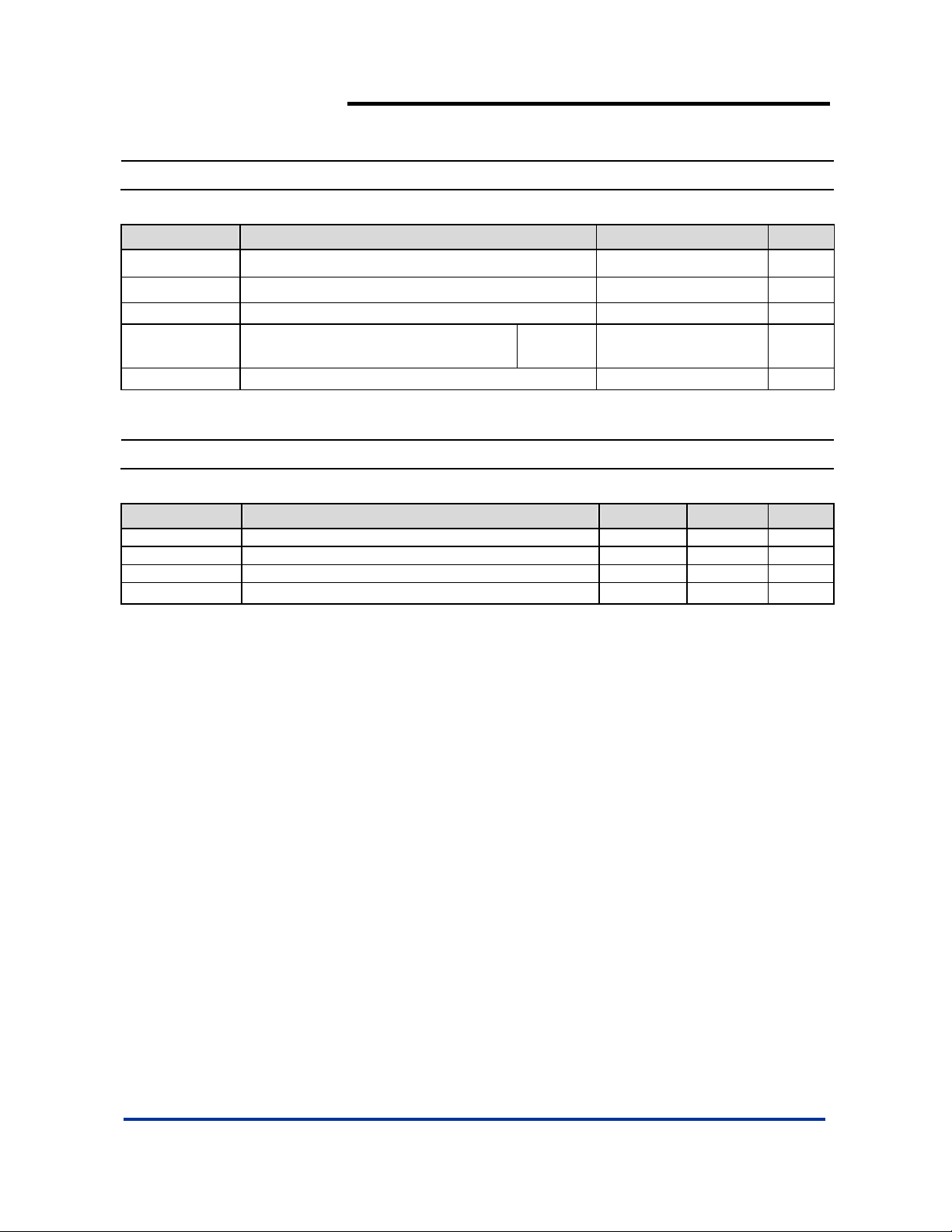
Absolute Maximum Ratings
Symbol Parameter Rating Unit
ESD HBM Human Body Model ESD Protection 3 KV
ESD MM Machine Model ESD Protection 450 V
VIN Input Voltage +6 V
PD Power Dissipation @ TA=25 ºC (Note 3)
TMJ Maximum Junction Temperature 150 ºC
Notes: 3. Maximum P
is under minimum recommended pad layout condition.
D
SOT89-3L
578 mW
Recommended Operating Conditions
Symbol Parameter Min Max Unit
VIN Input Voltage 2.5 5.5 V
I
Output Current 0 600 mA
OUT
TA Operating Ambient Temperature -40 85 ºC
TJ Operating Junction Temperature -40 125
ºC
AP7217D Rev. 2 3 of 9 FEBRUARY 2009
www.diodes.com © Diodes Incorporated
Page 4

AP7217D
1.2V 600mA CMOS LDO
Electrical Characteristics
= 25°C, C
(T
A
Symbol Parameter Test Conditions Min Typ. Max Unit
IQ Quiescent Current IO = 0mA - 40 60 μA
V
OUT
V
DROPOUT
I
OUT
I
LIMIT
I
SHORT
ΔV
ΔV
PSRR
= 1µF, C
IN
Output Volt age
Accuracy
V
OUT
Coefficient
Dropout Voltage I
Maximum Output
Current
= 1µF, VIN=5V, unless otherwise noted)
OUT
= 30mA 1.176 1.2 1.224 V
I
O
Temperature
-40°C to 85°C, I
= 600mA, V
OUT
600 - - mA
±100
= 30mA
OUT
= 1.2V - 850 1300 mV
OUT
-
- ppm /
Current Limit - 850 - mA
Short Circuit Current - 200 - mA
LINE
LOAD
Line Regulation 2.5V ≤ V
Load Regulation
(Note 4)
Power Supply
Rejection
Thermal Shutdown
Temperature
≤ 5.5V; I
IN
1mA ≤ I
1mA ≤ I
V
= 4.3V+0.5Vp-pAC,
IN
I
OUT
≤ 300mA 15 35 mV
OUT
≤ 600mA 30 55 mV
OUT
= 50mA
- 150 - ºC
= 30mA - 0.2 - %/V
OUT
F = 1KHz - 55 - dB
o
C
θ
JA
θ
JC
Notes: 4. Regulation is measured at constant junction temperature by low duty cycle pulse testing.
5. Test condition for SOT89-3L: Devices mounted on FR-4 substrate, single sided PC board, 2oz copper, with minimum recommended pad layout,
no air flow.
Thermal Shutdown
Hysteresis
Thermal Resistance
Junction-to-Ambient
Thermal Resistance
Junction-to-Case
- 30 - ºC
SOT89-3L (Note 5) - 173 - ºC/W
SOT89-3L (Note 5) - 51 - ºC/W
Typical Application
AP7217D Rev. 2 4 of 9 FEBRUARY 2009
www.diodes.com © Diodes Incorporated
Page 5

Typical Performance Characteristics
AP7217D
1.2V 600mA CMOS LDO
Dropout Voltage vs. Output Current
1000
900
800
700
600
500
400
300
Dropout Volt age (mV)
200
100
0
100 200 300 400 500 550 600
Output Current (mA)
900
880
860
840
820
Curren t Limit (m A )
800
780
Current Limit vs. Input Voltage
2.533.34 55.5
Input Voltage (V)
Quiescent Current vs. Input Voltage
30
29
28
27
26
25
24
23
22
Quiescent Current (uA)
21
20
2.5 3 3.3 4 5 5.5
Input Voltage (V)
Quiescent Current vs. Temperature
30
29
28
27
26
25
24
23
22
Quiescent Current (uA)
21
20
-40 0 25 85 100 125
Temperature (°C)
AP7217D Rev. 2 5 of 9 FEBRUARY 2009
www.diodes.com © Diodes Incorporated
Page 6

Typical Performance Characteristics (Continued)
Short Circuit Current vs. Input Voltage
220
215
210
205
200
195
190
Short Circuit Current (mA)
185
2.533.34 55.35.5
Inp ut Voltage (V)
Load Transient Response
AP7217D
1.2V 600mA CMOS LDO
AP7217D Rev. 2 6 of 9 FEBRUARY 2009
www.diodes.com © Diodes Incorporated
Page 7

Application Information
AP7217D
1.2V 600mA CMOS LDO
Input Capacitor
A 1μF ceramic capacitor is recommended to connect between IN
and GND pins to de couple input po wer supply glitc h and noise.
The amount of the capacitance may be increased without limit.
A lower ESR (Equivalent Series Resistance) capacitor allows the
use of less capac itance, while higher ESR type r equires more
capacitance. This input capacitor must be located as close as
possible to the device to assure input stability and less noise. For
PCB layout, a wide copper trace is required fo r both IN and GND.
Output Capacitor
The output capacitor is required to stabilize and help the transien t
response of the LDO. The AP7217D is designed to have
excellent transient response for most applications with a small
amount of output capacitance. The AP7217D is stable with any
small ceramic output capacitors of 1.0μF or higher value, and the
temperature coefficients of X7R or X5R type. Additional
capacitance helps to reduce undershoot and overshoot during
transient. For PCB layout, the output capacitor must be placed as
close as possible to OUT and GND pins, and keep the leads as
short as possible.
Thermal Considerations
Thermal Shutdown Protection limits power dissipation in
AP7217D. When the operation junction temperature exceeds
150°C, the Over Temperature Protection circuit sta rts the thermal
shutdown function and turns the pass element off. The pass
element turn on again after the junction temperature cools by
30°C. For continuous operation, do not exceed recommend
maximum operation junction temperature 125°C. The power
dissipation definition in device is:
PD = (VIN − V
OUT
) x I
+ VIN x IQ
OUT
The maximum power dissipation depends on the thermal
resistance of IC package, PCB layout, the rate of surroundings
airflow and temperature difference between junctions to ambient.
The maximum power dissipation can be calculated by following
formula:
P
= ( T
D(MAX)
Where T
125°C, T
to ambient thermal resistance.
J(MAX)
is the ambient temperature and the θJA is the junction
A
V
IN
- TA ) / θJA
J(MAX)
is the maximum operation junction temperature
I
IN
IN
OUT
I
OUT
V
OUT
AP7217D
C
IN
GND
Iq
Current Limit Protection
When output current at OUT pin is higher than current limit
threshold, the current limit protection will be triggered and clamp
the output current to approximately 850mA to prevent
over-current and to protect the regulator from damage due to
overheating.
Short circuit protection
When V
200mV, short circuit protection will be triggered and clamp the
output current to approximately 200mA.
pin is shorted to GND or V
OUT
voltage is less than
OUT
C
ESR
OUT
AP7217D Rev. 2 7 of 9 FEBRUARY 2009
www.diodes.com © Diodes Incorporated
Page 8

Marking Information
(1) SOT89-3L
( Top View )
XX : N4 : AP7217D-12
X X
Y W
1 32
X
Package Information (All Dimensions in mm)
(1) Package Type: SOT89-3L
1.40/1.75
Typ 1.60
Y : Year : 0~9
W
X
AP7217D
1.2V 600mA CMOS LDO
: Week : A~Z : 1~26 week;
a~z : 27~52 week;
z represents 52 and 53 week
: Internal code
A~Z : Green
1.7
2.7
3.94/4.25
1.45/1.55
Typ 1.50
80(2x)
0.36/0.48
2.90/3.10
4.40/4.60 Typ 4.50
0.41/0.53
Typ 0.42
Typ 3.00
Typ 0.47
0.36/0.48
Typ 0.42
2.35/2.60 Typ 2.48
1.20
0.80/
Land Pattern Recommendation (Unit: mm)
Typ 1.50
1.40/1.60
0.35/0.43
Typ 0.39
0.9
50(2x)
0.4
1.5
1.9
1.3
AP7217D Rev. 2 8 of 9 FEBRUARY 2009
www.diodes.com © Diodes Incorporated
Page 9

AP7217D
1.2V 600mA CMOS LDO
IMPORTANT NOTICE
Diodes Incorporated and its subsidiaries reserve the right to make modifications, enhancements, improvements, corrections or other changes without further
notice to any product herein. Diodes Incorporated does not assume any liability arising out of the application or use of any product described herein; neither
does it convey any license under its patent rights, nor the rights of others. The user of products in such applications shall assume all risks of such use and will
agree to hold Diodes Incorporated and all the companies whose products are represented on our website, harmless against all damages.
LIFE SUPPORT
Diodes Incorporated products are not authorized for use as critical components in life support devices or systems without the expressed written approval of the
President of Diodes Incorporated.
AP7217D Rev. 2 9 of 9 FEBRUARY 2009
www.diodes.com © Diodes Incorporated
 Loading...