

Page 1
AP7217A
3.3V 600mA CMOS LDO
Features
• Very Low Dropout Voltage
• Low Current Consumption: Typ. 50µA
• Output Voltage: 3.3V
• Guaranteed 600mA (min) Output
• Input Range up to 5.5V
• Current Limiting
• Stability with Low ESR Capacitors
• Thermal shutdown Protection
• Low Temperature Coeff icient
• SOP-8L and SOP-8L-EP: Available in “Green” Molding
Compound (No Br, Sb)
• Lead Free Finish/ RoHS Compliant (Note 1)
Applications
• HD/ Blue Ray DVD & MP3/4 Players
• CD and MP3 Players
• Cellular and PCS Phones
• Digital Still Camera
• Hand-Held Computers
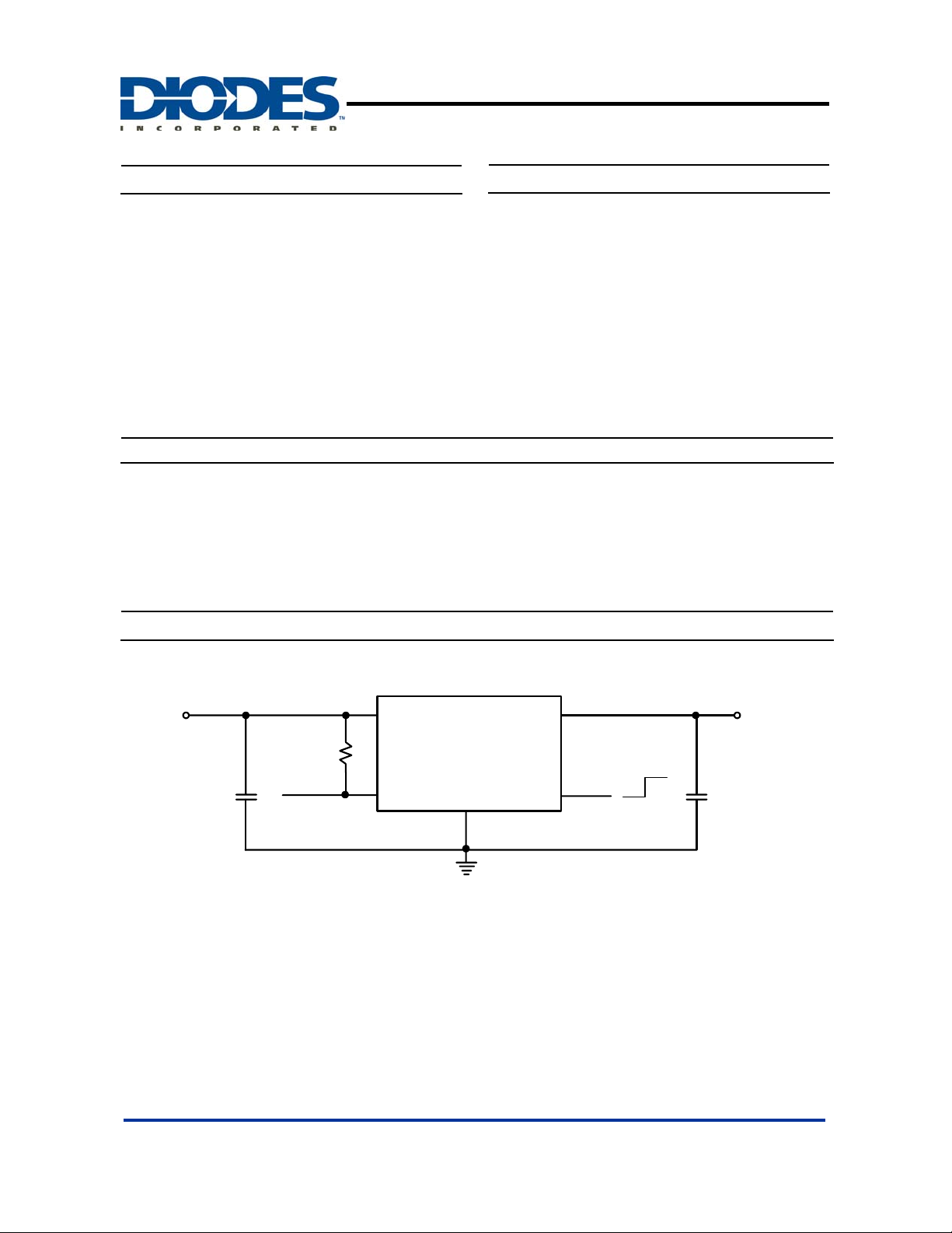
Typical Application Circuit
U1
4
V
IN
V
General Description
The AP7217A low-dropout linear regulator operates from a 3.3V
to 5.5V supply and delivers a guaranteed 600mA (min)
continuous load current.
The high-accuracy output voltage is preset to an internally
trimmed voltage. An active-low open-drain reset output remains
asserted for at least 200ms (TYP) after output voltage reaches
regulation.
The space-saving SOP-8L and SOP-8L-EP packages are
suitable for “pocket” and hand-held application.
OUT
2
VR
OUT
IN
V
C
1uF
100K
IN
VD
OUT
6
VD
OUT
AP7217A
GND
EN
ON
8
OFF
C
1uF
OUT
7
AP7217A Rev. 3 1 of 10 OCTOBER 2009
DS31423 www.diodes.com © Diodes Incorporated
Page 2
8
L-EP
Ordering Information
AP7217A
3.3V 600mA CMOS LDO
AP 7217A - 33 XX G - 13
Output voltage
33 : 3.3V
Package
S : SOP-8L
G : Green
PackingGreen
13 : Tape & Reel
SP : SOP-8L-EP
Device
Package
Code
Packaging
(Note 2)
Quantity Part Number Suffix
13” Tape and Reel
AP7217A-33SG-13 S SOP-8L 2500/Tape & Reel -13
AP7217A-33SPG-13 SP SOP-8L-EP 2500/Tape & Reel -13
Notes: 1. EU Directive 2002/95/EC (RoHS). All applicable RoHS exemptions applied. Please visit our website at
http://www.diodes.com/products/lead_free.html
2. Pad layout as shown on Diodes Inc. suggested pad layout document AP02001, which can be found on our website at
http://www.diodes.com/datasheets/ap02001.pdf.
.
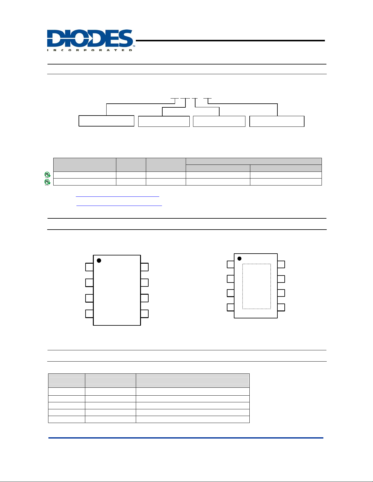
Pin Assignments
( Top View )
1
2
OUT
3
V
4
IN
EN
8
GND
7
VD
6
OUTGND
GND
5
GND
VR
GND
OUT
V
1
2
3
4
IN
( Top View )
AP7217A
EN
8
GND
7
VD
6
OUT
GND
5
GND
VR
SOP-8L
SOP-
Pin Descriptions
Pin Name Pin No. Description
GND 1, 3, 5, 7 Ground
VR
2 Voltage Output
OUT
VIN 4 Supply Voltage
VD
6 VD Output (Reset on I/P)
OUT
EN 8 Enable (VR On/Off)
AP7217A Rev. 3 2 of 10 OCTOBER 2009
DS31423 www.diodes.com © Diodes Incorporated
Page 3
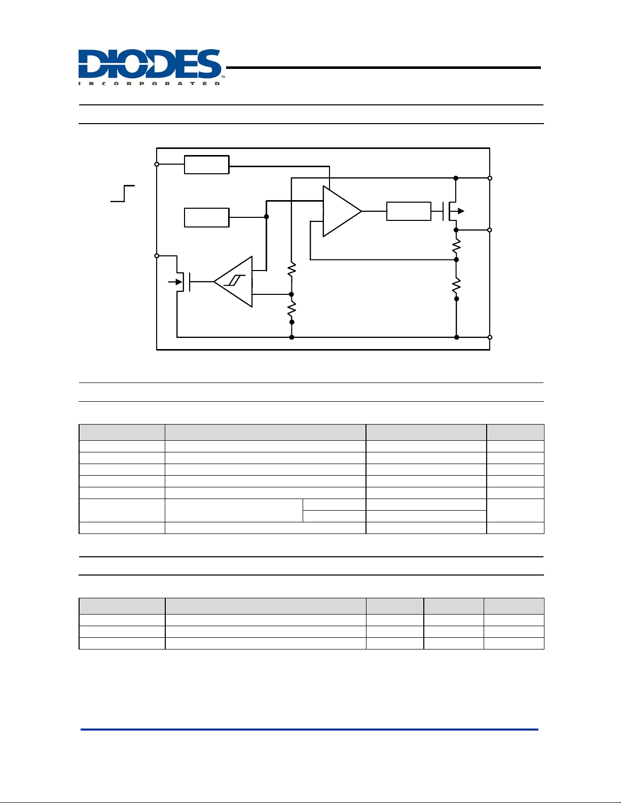
Block Diagram
AP7217A
3.3V 600mA CMOS LDO
Off
VD
EN
On
OUT
Enable
Bandgap
1.2V
+
R3
-
ERROR
AMP
+
Current
Limit
R1
R2
-
VD Comp.
R4
Absolute Maximum Ratings
Symbol Parameter Rating Unit
ESD HBM Human Body Model ESD Protection 3.5 KV
ESD MM Machine Model ESD Protection 500 V
VIN Input Voltage +6 V
I
Output Current PD/ (VIN-VO) mA
OUT
VR
Output Voltage GND - 0.3 ~ VIN+ 0.3 V
OUT
PD Power Dissipation
SOP-8L 1010
SOP-8L-EP 1650
TJ Operating Junction Temperature Range -40 to +125 ºC
Recommended Operating Conditions
Symbol Parameter Min Max Unit
VIN Input Voltage 3.3 5.5 V
I
Output Current 0 600 mA
OUT
TA Operating Ambient Temperature -40 85 ºC
V
IN
VR
GND
OUT
mW
AP7217A Rev. 3 3 of 10 OCTOBER 2009
DS31423 www.diodes.com © Diodes Incorporated
Page 4

Electrical Characteristics
(TA = 25°C, C
Symbol Parameter Test Conditions Min Typ. Max Unit
V
∆V
LINE
VD Hysteresis
Notes: 3. Test condition for SOP-8L: Device mounted on FR-4 substrate PC board, 2oz copper, with minimum recommended pad layout.
double sided FR-4 PCB.
AP7217A Rev. 3 4 of 10 OCTOBER 2009
DS31423 www.diodes.com © Diodes Incorporated
= 1µF, C
IN
OUT
= 1µF, V
IQ Quiescent Current IO = 0mA - 50 80 µA
I
Standby Current
STB
Output Voltage
Accuracy
V
Temperature
OUT
VR
OUT
Coefficient
DROPOUT
∆V
PSRR
Dropout Voltage
I
OUT
I
LIMIT
I
Short Circuit Current V
short
/∆VIN/V
OUT
Maximum Output
Current
Current Limit V
Line Regulation 4.3V ≤ V
OUT
Load Regulation 1mA ≤ I
Power Supply
Rejection
VEH Output ON 1.6 V
VEL
EN Input Threshold
IEN Enable Pin Current -0.1 0.1 µA
VDF
Range
Detect fall voltage 3.23 3.3 3.37 V
V
IVDout VD Supply Current
tRP V
θ
JA
θ
JC
4. Test condition for SOP-8L-EP: Device mounted on 2oz copper, minimum recommended pad layout on top & bottom layer with thermal vias,
Delay Time V
DOUT
Thermal Resistance
Junction-to-Ambient
Thermal Resistance
Junction-to-Case
= VIN, unless otherwise noted)
EN
V
= Off
EN
V
= 5.0V
IN
= 30mA, V
I
O
-40°C to 85°C, I
I
= 300mA 350 400
OUT
I
= 600mA 800 900
OUT
V
= 5.3V 600 mA
IN
= 5.3V 750 mA
IN
= 5.3V 50 mA
IN
= 4.3V+ 0.5Vp-pAC,
V
IN
I
= 50mA
OUT
Output OFF 0.25 V
Hysteresis
VDout = 0.5V
VIN = 2.0V
= 1.8V to VDF+ 1V 180 200 - mSec
IN
SOP-8L (Note 3) 134
SOP-8L-EP (Note 4) 82
SOP-8L (Note 3) 28
SOP-8L-EP (Note 4) 12
≤ 5.5V; I
IN
≤ 100mA, V
OUT
3.0V
AP7217A
3.3V 600mA CMOS LDO
15 25
= 5V 3.234 3.300 3.366 V
IN
±100
= 30mA
OUT
= 30mA 0.01 ±0.2 %/V
OUT
= 5.3V 15 50 mV
IN
F = 1KHz 55 dB
V
x1.02
DF
V
DF
x1.05
20
30
ppm /
V
DF
x1.08
µA
mV
V
mA
ºC/W
ºC/W
o
C
Page 5

Typical Performance Characteristics
AP7217A
3.3V 600mA CMOS LDO
Output Current vs. Dropout Voltage
900
800
700
600
500
400
300
200
Dropout Voltage (mV)
100
0
30mA 100mA 300mA 600mA
(Vout=3.3V)
Output Current
Quiescent Current vs. Temperature
75
70
65
60
55
50
Quiescent Current (uA)
45
40
-40℃ 0℃ 25℃ 85℃ 100℃
Temperature
Input Voltage vs. Max Iout
800
700
600
500
400
300
Max Iout (mA)
200
100
0
3.6V 4.3V 5.0V 5. 3 5.5V
Input Voltage
Quies cent Current vs. Input Voltage
80
70
60
50
40
30
20
Quiescent Current (uA)
10
0
3.6V 56V 58V 61V 5.5V
Input Voltage
AP7217A Rev. 3 5 of 10 OCTOBER 2009
DS31423 www.diodes.com © Diodes Incorporated
Page 6

Typical Performance Characteristics (Continued)
AP7217A
3.3V 600mA CMOS LDO
Short Current vs. Input Voltage
65
64
63
62
61
60
59
58
Short Current (mA)
57
56
55
3.6V 4.3V 5V 5.3V 5.5V
Input Voltage
Stand-by Current vs. Input Voltage
24
21
18
Short Current vs. Temperature
64
62
60
58
56
54
(Vin=5.5V)
Short Current (mA)
52
50
-40℃ 25℃ 85℃ 105℃
Temperature
Stand-by Current vs. Temperature
35
30
25
20
15
15
Stand-by Current (uA)
12
3.6V 4V 4.3V 5V 5.5V
Input Voltage
10
Stand-by Current (uA)
5
0
-40℃ 0℃ 25℃ 85℃ 105℃ 125℃
Temperature
Load Transient Response Load Transient Response
AP7217A Rev. 3 6 of 10 OCTOBER 2009
DS31423 www.diodes.com © Diodes Incorporated
Page 7

Timing Diagram
1.6V
t
RP
200mSec-TYP.
AP7217A
3.3V 600mA CMOS LDO
V
IN
VD
OUT
EN
VR
OUT
Application Note
Input Capacitor
A 1µF ceramic capacitor is recommended to connect between IN
and GND pins to de couple input po wer supply glitc h and noise.
The amount of the capacitance may be increased without limit. A
lower ESR (Equivalent Series Resistance) capacitor allows the
use of less capac itance, while higher ESR type r equires more
capacitance. This input capacitor must be located as close as
possible to the device to assure input stability and less noise. For
PCB layout, a wide copper trace is required fo r both IN and GND.
Output Capacitor
The output capacitor is required to stabilize and help the transien t
response of the LDO. The AP7217A is designed to have
excellent transient response for most applications with a small
amount of output capacitance. The AP7217 is stable with any
small ceramic output capacitors of 1.0µF or higher value, and the
temperature coefficients of X7R or X5R type. Additional
capacitance helps to reduce undershoot and overshoot during
transient. For PCB layout, the output capacitor must be placed as
close as possible to OUT and GND pins, and keep the leads as
short as possible.
ENABLE/SHUTDOWN Operation
The AP7217A is turned on by setting the EN pin high, and is
turned off by pulling it low. If this feature is not used, the EN pin
should be tied to IN pin to keep the regulator output on at all time.
To ensure proper operation, the signal source used to drive the
EN pin must be able to swing above and below the specified
turn-on/off voltage thresholds listed in the Electrical
Characteristics section under V
Thermal Considerations
Thermal Shutdown Protection limits power dissipation in
AP7217A. When the operation junction temperature exceeds
150°C, the Over Temperature Protection circuit starts the the rma l
shutdown function and turns the pass element off. The pass
element turn on again after the junction temperature cools by
40°C. For continuous operation, do not exceed absolute
maximum operation junction temperature 125°C. The power
dissipation definition in device is:
VR
EN=0 0V Φ
EN=1 3.3V Φ
PD = (VIN − VOUT) x I
The maximum power dissipation depends on the thermal
resistance of IC package, PCB layout, the rate of surroundings
airflow and temperature difference between junction to ambient.
The maximum power dissipation can be calculated by following
formula :
P
= ( T
D(MAX)
Where T
125°C, T
to ambient thermal resistance.
J(MAX)
is the ambient temperature and the θJA is the junction
A
- TA ) / θJA
J(MAX)
is the maximum operation junction temperature
and VIH.
IL
VD
OUT
+ VIN x IQ
OUT
OUT
AP7217A Rev. 3 7 of 10 OCTOBER 2009
DS31423 www.diodes.com © Diodes Incorporated
Page 8

Application Note (Continued)
Vin Vout
Current Limit Protection
When output current at OUT pin is higher than current limit
threshold, the current limit protection will be triggered and clamp
the output current to approximately 750mA to prevent
over-current and to protect the regulator from damage due to
overheating.
Marking Information
(1) SOP-8L
Iin Iout
IN OUT
C Co
AP7217A
GND
Iq
ESR
( Top View )
AP7217A
3.3V 600mA CMOS LDO
Short circuit protection
When VR
200mV, short circuit protection will be triggered and clamp the
output current to approximately 50mA.
VD
OUT
---Open-Drain Active-Low reset output--In general, VD
The AP7217A microprocess (uP) supervisory circuitry asserts a
guaranteed logic-low reset during power-up and power-down.
Reset is asserted asserts when V
and remain asserted for at least t
threshold.
As long as V
logic "0". When V
asserted after a time delay defined by t
pin is shorted to GND or VR
OUT
(reset output)
is pulled up by a resistor (100Kohm) to VIN.
OUT
is lower than the reset threshold, VD
IN
become higher than VTH, a logic "1" is
IN
voltage is less than
OUT
is below the reset threshold
IN
after VIN rises above the reset
RP
remains at
OUT
.
RP
(2) SOP-8L-EP
Logo
Part Number
Logo
Part No.
8
5
7217A-33
YY
WW X
X
41
( Top View )
8
5
7217A-33
WW X
YY
X
41
YY
: Year : 08, 09,10~
WW : Week : 01~52; 52
represents 52 and 53 week
X
: Internal Code
G : Green
G : Green
YY
: Year : 08, 09,10~
: Week : 01~52; 52
WW
E
represents 52 and 53 week
X
: Internal Code
SOP-8L-EP
AP7217A Rev. 3 8 of 10 OCTOBER 2009
DS31423 www.diodes.com © Diodes Incorporated
Page 9

Package Information (All Dimensions in mm)
(1) Package Type: SOP-8L
0.254
3.85/3.95
5.90/6.10
0.10/0.20
Detail "A"
0.62/0.82
Gauge Plane
Seating Plane
AP7217A
3.3V 600mA CMOS LDO
7°~9°
1.27typ
8x-0.60
6x-1.27
8x-1.55
Land Pattern Recommendation
0.3/0.5
4.85/4.95
(Unit: mm)
(2) Package Type: SOP-8L-EP
3.85/3.95
1
7°~9°
1.30/1.50
1.27typ
1
8x-0.60
0.3/0.5
4.85/4.95
1.30/1.50
1.75max.
5.4
Detail "A"
7°~9°
45°
5.90/6.10
0.35max.
0.15/0.25
1.75max.
0/0.13
Exposed pad
0.35max.
0.15/0.25
Detail "A"
45°
3.70/4.10
0.62/0.82
7°~9°
3.3Ref.
Bottom View
0.254
Gauge Plane
Seating Plane
Detail "A"
0°/8°
Exposed pad
2.4Ref.
1
5.4
6x-1.27
8x-1.55
Land Pattem Recommendation
(Unit:mm)
AP7217A Rev. 3 9 of 10 OCTOBER 2009
DS31423 www.diodes.com © Diodes Incorporated
Page 10

AP7217A
3.3V 600mA CMOS LDO
IMPORTANT NOTICE
DIODES INCORPORATED MAKES NO WARRANTY OF ANY KIND, EXPRESS OR IMPLIED, WITH REGARDING TO THIS
DOCUMENT, INCLUDING, BUT NOT LIMITED TO, THE IMP LIED WARRAN TIES OF MERCHA NTABILITY A ND FITNESS FOR A
PARTICULAR PURPOSE (AND THEIR EQUIVALENTS UNDER THE LAWS OF ANY J URISDICTION).
Diodes Incorporated and its subsidiaries reserve the right to make modifications, enhancements, improvements, corrections or other
changes without further notice to this document and any product described herein. Diodes Incorporated does not assume any
liability arising out of the application or use of this document or any product described herein; neither does Diodes Incorporated
convey any license under its patent or trademark rights, nor the rights of others. Any Customer or user of this document or products
described herein in such applications shall assume all risks of such use and will agree to hold Diodes Incorporated and all the
companies whose prod ucts are represented on Diodes Incorporated websit e , harmless against all damage s.
Diodes Incorporat ed do es no t warrant or ac ce pt any li abil it y whatso ever in resp ect of any pr oduc ts purc has ed t hrough unaut hori zed
sales channel.
Should Customers purchase or use Diodes Incorporated products for any unintended or unauthorized application, Customers shall
indemnify and hold Di odes Inc orporat ed and its r epres entat ives harm less ag ainst al l claims , dam ages, expens es, a nd attorne y fees
arising out of, directly or indirectly, any claim of personal injury or death associated with such unintended or unauthorized
application.
Products described herein may be covered by one or more United States, international or foreign patents pending. Product names
and markings noted herein may also be covered by one or more United States, international or foreign trademarks.
LIFE SUPPORT
Diodes Incorporated products are specifically not authorized for use as critical components in life support devices or systems
without the express written approval of the Chief Executive Officer of Diodes Incorporated. As used herein:
A. Life support devices or systems are devices or systems which:
1. are intended to implant into the body, or
2. support or sustain life and whose failure to perform when properly used in accordance with instructions for use provided
in the labeling can be reasonably expected to result in significant injury to the user.
B. A critical component is any component in a life support device or system whose failure to perform can be reasonably expected
to cause the failure of the life support device or to affect its safety or effectiveness.
Customers represent that they have all necessary expertise in the safety and regulatory ramifications of their life support devices or
systems, and acknowledge and agree that they are solely responsible for all legal, regulatory and safety-related requirements
concerning their products and any use of Diodes Incorporated products in such safety-critical, life support devices or systems,
notwithstanding any devices- or systems-related information or support that may be provided by Diodes Incorporated. Further,
Customers must fully indemnify Diodes Incorporated and its representatives against any damages arising out of the use of Diodes
Incorporated products in such safety-critical, life support devices or systems.
Copyright © 2009, Diod es In c orp orat e d
www.diodes.com
AP7217A Rev. 3 10 of 10 OCTOBER 2009
DS31423 www.diodes.com © Diodes Incorporated
 Loading...