Diodes AP7215 User Manual

AP7215
600mA CMOS LDO
Features
• Very Low Dropout Voltage
• Low Current Consumption: Typ. 50μA
• Output Voltage: 3.3V
• Guaranteed 600mA Output
• Input Range up to 5.5V
• Current Limit Protection
• Stable with either electrolytic capacitor or low-ESR
MLCC (multi-layer ceramic capacitor) Low
Temperature Coefficient
• SOP-8L and SOT89-3L: Available in “Green” Molding
Compound (No Br, Sb)
• Lead Free Finish / RoHS Compliant (Note 1)
Applications
• HD/Blue-Ray DVD & MP3/4 Players
• Mobile Handsets and Smart Phones
• Digital Still Camera
• Hand-Held Computers
Ordering Information
General Description
The AP7215 low-dropout linear regulator operates from a 3.3V to
5.5V supply and delivers a guaranteed 600mA continuous load
current.
The high-accuracy output voltage is preset to an internally
trimmed voltage. An active-low open-drain reset output remains
asserted for at least 20ms (TYP) after input voltage rises above
the reset threshold.
The space-saving SOP-8L and SOT89-3L package are suitable
for “pocket” and hand-held applications.
AP7215 - 33 X G - 13
Output voltage
33 : 3.3V
Package
S : SOP-8L
G : Green
PackingGreen
13 : Tape & Reel
Y : SOT89-3L
Device
Package
Code
Packaging
(Note 2)
Quantity Part Number Suffix
13” Tape and Reel
AP7215-33SG-13 S SOP-8L 2500/Tape & Reel -13
AP7215-33YG-13 Y SOT89-3L 2500/Tape & Reel -13
Notes: 1. EU Directive 2002/95/EC (RoHS). All applicable RoHS exemptions applied, see EU Directive 2002/95/EC Annex Notes.
2. Pad layout as shown on Diodes Inc. suggested pad layout document AP02001, which can be on our website at
http://www.diodes.com/datasheets/ap02001.pdf
.
AP7215 Rev. 1 1 of 11 FEBRUARY 2009
www.diodes.com © Diodes Incorporated

Pin Assignments
(1) SOP-8L (2) SOT89-3L
( Top View )
NC
1
OUT
NC
V
2
3
4
IN
VR
Pin Descriptions
Pin Name
NC 1, 3 , 5 - No Connection
VR
2 3 Voltage Output
OUT
VIN 4 2 Supply Voltage
VD
6 - VD Output Voltage (Reset Output)
OUT
GND 7 1 Ground
EN 8 - Enable (VR
SOP-8L SOT89-3L
Pin No.
EN
8
GND
7
VD
6
OUT
5
NC
OUT
( Top View )
Tab is V
Description
ON/OFF)
AP7215
600mA CMOS LDO
3
2
1
IN
VR
OUT
V
IN
GND
AP7215 Rev. 1 2 of 11 FEBRUARY 2009
www.diodes.com © Diodes Incorporated

)
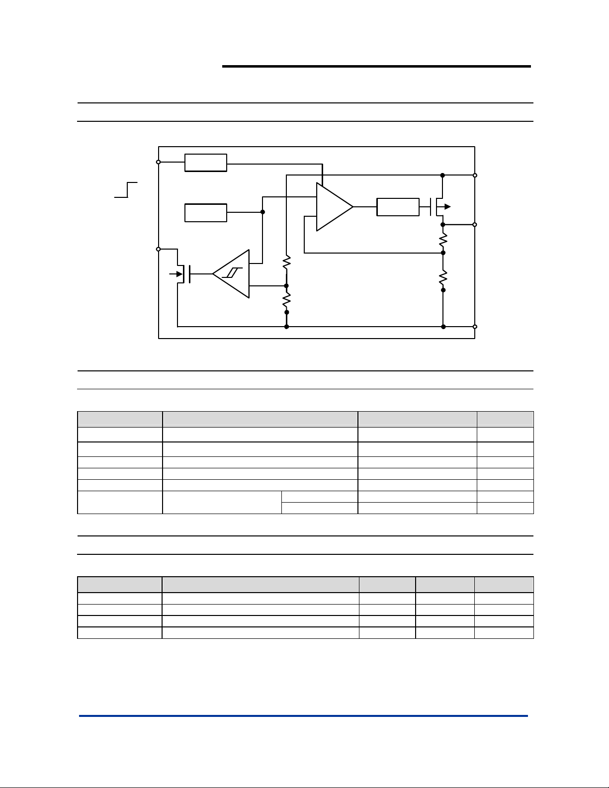
Block Diagram
AP7215
600mA CMOS LDO
Off
VD
EN
On
OUT
Enable
Bandgap
1.2V
+
R3
-
ERROR
AMP
+
Current
Limit
R1
R2
-
VD Comp.
R4
Absolute Maximum Ratings
Symbol Parameter Rating Unit
ESD HBM Human Body Model ESD Protection 2 KV
ESD MM Machine Model ESD Protection 350 V
VIN Input Voltage +6 V
VR
Output Voltage GND - 0.3 ~ VIN+ 0.3 V
OUT
T
Maximum Junction Temperature 150 ºC
J(MAX
PD Power Dissipation
SOP-8L 1.2 W
SOT89-3L 0.79 W
Recommended Operating Conditions
Symbol Parameter Min Max Unit
VIN Input Voltage 3.3 5.5 V
I
Output Current 0 600 mA
OUT
TJ Operating Junction Temperature Range -40 125 ºC
TA Operating Ambient Temperature -40 85 ºC
V
IN
VR
GND
OUT
AP7215 Rev. 1 3 of 11 FEBRUARY 2009
www.diodes.com © Diodes Incorporated

AP7215
600mA CMOS LDO
Electrical Characteristics
= 25°C, C
(T
A
Symbol Parameter Test Conditions Min Typ. Max Unit
I
I
VR
ΔVR
/ΔTA/VR
OUT
VDO Dropout Voltage
I
I
I
SHORT
ΔVR
OUT
ΔVR
PSRR
VEH
V
IVD
Notes: 3. Test conditions for SOP-8L, SOT89-3L: Device mounted on FR-4 substrate, single sided PC board, 2oz copper, with minimum recommended
AP7215 Rev. 1 4 of 11 FEBRUARY 2009
www.diodes.com © Diodes Incorporated
= 1µF, C
IN
Quiescent Current I
CCQ
Standby Current
STBY
OUT
OUT
Current Limit V
LIMIT
Output Voltage
Accuracy
VR
OUT
Coefficient
Maximum Output
Current
= 1µF, VIN=5.0V, V
OUT
Temperature
OUT
= VIN, unless otherwise noted)
EN
= 0mA - 50 80 μA
OUT
V
= GND
EN
= 5.0V
V
IN
= 30mA, V
I
OUT
=-40°C to 85°C, I
T
A
= 30mA 60 100 mV
I
OUT
I
= 100mA 100 250 mV
OUT
= 5.3V 600 mA
V
IN
= 5.3V 750 mA
IN
= 5V 3.234 3.300 3.366 V
IN
= 30mA
OUT
15 30
±100
ppm /
μA
Short Circuit Current VIN= 5.3V 50 mA
/ΔVIN/VR
T
VEL Output OFF 0.25 V
OUT
OU
Line Regulation 4.3V ≤ V
Load Regulation 1mA ≤ I
Power Supply
Rejection
EN Input Threshold
≤ 5.5V, I
IN
≤ 100mA, V
OUT
= 4.3V+ 0.5Vp-pAC,
V
IN
I
= 50mA
OUT
= 30mA 0.01 ±0.2 %/V
OUT
= 5.3V 15 50 mV
IN
F= 1KHz 55 dB
Output ON 1.6 V
IEN Enable Pin Current -0.1 0.1 μA
VDF
HYS
VD
OUT
tRP VD
θ
JA
θ
JC
pad layout.
VIN Detection Voltage Detect VD
VDF Hysteresis
Range
Sink Current
OUT
Delay Time 10 20 40 ms
OUT
Thermal Resistance
Junction-to-Ambient
Thermal Resistance
Junction-to-Case
VD
OUT
VD
OUT
SOP-8L (Note 3) 124
SOT89-3L (Note 3) 173
SOP-8L (Note 3) 25
SOT89-3L (Note 3) 42
fall 3.83 3.91 3.98 V
OUT
= 0.5V, V
= 0.5V, V
= 2.0V
IN
= 3.0V
IN
V
x1.02
V
DF
DF
x1.05
20 mA
30
V
DF
x1.08
V
ºC/W
ºC/W
o
C
 Loading...