Diodes AP7176B User Manual
A
P7176B
Description
The AP7176B is a 3.0A ultra low-dropout (LDO) linear regulator that
features an enable input and a power-good output.
The enable input and power-good output allow users to configure
power management solutions that can meet the sequencing
requirements of FPGAs, DSPs, and other applications with different
start-up and power-down requirements.
The AP7176B features two supply inputs, for power conversion
supply and control. With the separation of the control and the power
input very low dropout voltages can be reached and power dissipation
is reduced.
A precision reference and feedback control deliver 1.5% accuracy
over load, line, and operating temperature ranges.
The AP7176B is available in SO-8EP, MSOP-8EP and U-DFN3030-
NEW PRODUCT
10 package with an exposed PAD to reduce the junction to case
resistance and extend the temperature range it can be used in.
Features
• VIN Range: 1.2V to 3.65V V
• Adjustable Output Voltage
• Continuous Output Current I
• Fast Transient Response
• Power on reset monitoring on V
• Internal Soft-Start
• Stable with Low ESR MLCC Capacitors
• Totally Lead-Free & Fully RoHS Compliant (Notes 1 & 2)
• Halogen and Antimony Free. “Green” Device (Note 3)
3.0V to 5.5V
CNTL
= 3A
OUT
CNTL
and VIN
3A ULTRA LOW DROPOUT LINEAR REGULATOR WITH ENABLE
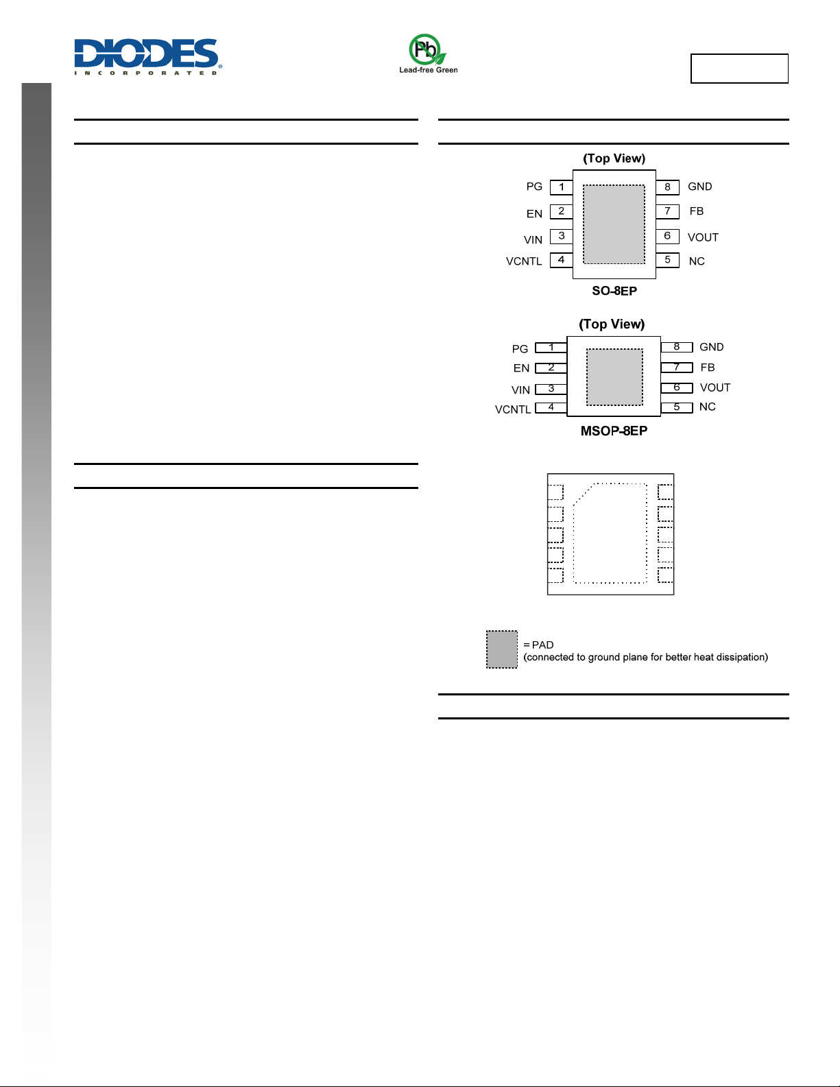
Pin Assignments
(Top View)
1
VOUT
2
VOUT
3
VOUT
FB
PG
4
5
GND
U-DFN3030-10
10
VCNTL
9
VIN
8
11
VIN
7
VIN
6
EN
Applications
• Notebook
• PC
• Netbook
• Wireless Communication
• Server
• Motherboard
• Dongle
• Front Side Bus VTT (1.2V/3.3A)
Notes: 1. No purposely added lead. Fully EU Directive 2002/95/EC (RoHS) & 2011/65/EU (RoHS 2) compliant.
2. See http://www.diodes.com/quality/lead_free.html for more information about Diodes Incorporated’s definitions of Halogen- and Antimony-free, "Green"
and Lead-free.
3. Halogen- and Antimony-free "Green” products are defined as those which contain <900ppm bromine, <900ppm chlorine (<1500ppm total Br + Cl) and
<1000ppm antimony compounds.
AP7176B
Document number: DS35818 Rev.3 - 2
www.diodes.com
1 of 14
April 2014
© Diodes Incorporated
A
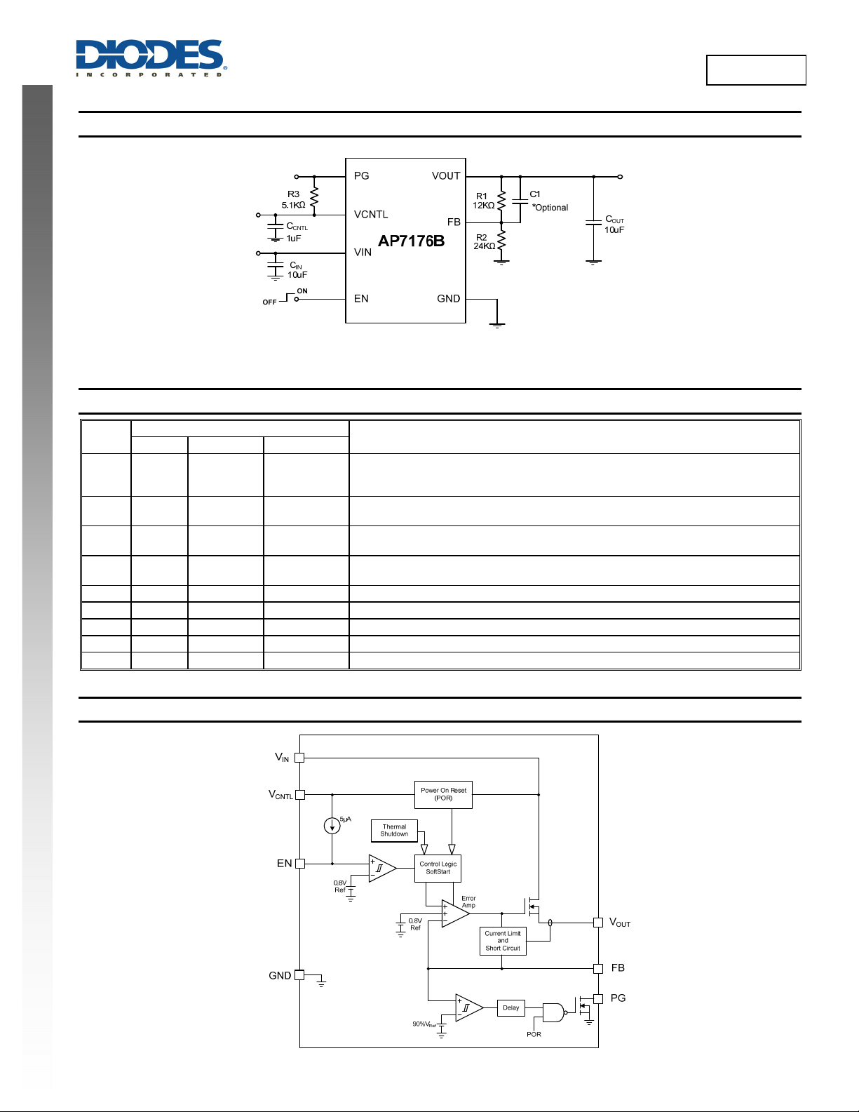
Typical Applications Circuit
Pin Descriptions
NEW PRODUCT
Pin
Name
VCNTL 4 4 10
V
GND 8 8 11 Ground
PAD EP EP EP Exposed pad connected to GND for good thermal conductivity
SO-8EP MSOP-8EP U-DFN3030-10
PG 1 1 5
EN 2 2 6
VIN 3 3 7,8,9
NC 5 5 No Connection
6 6 1,2,3 Power output pin
OUT
FB 7 7 4 Feedback to set the output voltage via an external resistor divider between V
Pin Number
Functional Block Diagram
P7176B
Figure 1 Typical Application Circuit
Power Good.Output open drain to indicate the status of V
This pin is pulled low when the voltage is outside the limits, during thermal shutdown and
if either V
Enable Pin. Driving this pin low will disable the part. When left floating an internal current
source will pull this pin high and enable it.
Power Input Pin for current supply. Connect a decoupling capacitor (10µF) as close as
possible to the pin for noise filtering
BIAS supply for the controller, recommended 5V. Connect a decoupling capacitor (1µF)
as close as possible to the pin for noise filtering.
CNTL
Function
or VIN go below their thresholds.
via monitoring the FB pin.
OUT
OUT
and GND
AP7176B
Document number: DS35818 Rev.3 - 2
2 of 14
www.diodes.com
April 2014
© Diodes Incorporated
A
P7176B
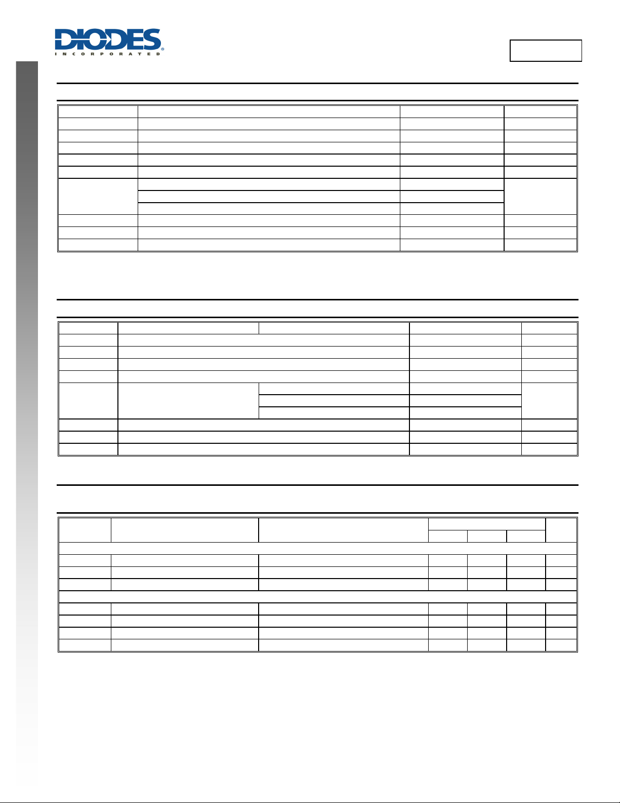
Absolute Maximum Ratings (Note 4) (@T
Symbol Parameter Rating Unit
VIN V
V
V
CNTL
V
V
OUT
PD
TJ Maximum Junction Temperature 150 °C
T
Storage Temperature -65 to +150 °C
STG
T
Maximum Lead Soldering Temperature, 10 Seconds 260 °C
SDR
Note: 4. Stresses greater than the 'Absolute Maximum Ratings' specified above, may cause permanent damage to the device. These are stress ratings only;
functional operation of the device at these or any other conditions exceeding those indicated in this specification is not implied. Device reliability may
be affected by exposure to absolute maximum rating conditions for extended periods of time.
Supply Voltage (VIN to GND) -0.3 to +4.0 V
IN
Supply Voltage (V
CNTL
to GND Voltage -0.3 to VIN +0.3 V
OUT
to GND) -0.3 to +7.0 V
CNTL
PG to GND Voltage -0.3 to +7.0 V
EN, FB to GND Voltage -0.3 to V
Power Dissipation (SO-8EP) 1.7
Power Dissipation (U-DFN3030-10) 1.9
= +25°C, unless otherwise specified.)
A
+0.3 V
CNTL
W Power Dissipation (MSOP-8EP) 1.5
NEW PRODUCT
Recommended Operating Conditions (@T
Symbol Parameter Test Condition Range Unit
V
V
CNTL
VIN V
V
V
OUT
I
V
OUT
C
V
OUT
E
ESR of V
SRCOUT
Supply Voltage 3.0 to 5.5 V
CNTL
Supply Voltage 1.2 to 3.65 V
IN
Output Voltage (when V
OUT
Output Current 0 to 3 A
OUT
Output Capacitance
OUT
Output Capacitor 0 to 200 m
OUT
CNTL
TA Ambient Temperature -40 to +85 °C
TJ Junction Temperature -40 to +125 °C
Electrical Characteristics (Specifications apply over V
@TA = +25°C, unless otherwise specified.)
Symbol Parameter Conditions
SUPPLY CURRENT
IV
V
CNTL
ISD V
Supply Current EN = V
CNTL
Supply Current at Shutdown EN = GND — 15 30 µA
CNTL
VIN Supply Current at Shutdown EN = GND, V
POWER-ON-RESET (POR)
Rising V
V
CNTL
Rising V
POR Threshold 2.50 2.70 2.95 V
CNTL
POR Hysteresis — 0.4 — V
POR Threshold 0.8 0.9 1.0 V
IN
VIN POR Hysteresis — 0.5 — V
AP7176B
Document number: DS35818 Rev.3 - 2
= +25°C, unless otherwise specified.)
A
- V
>1.9V) 0.8 to VIN – V
OUT
= 3A at 25% nominal V
I
OUT
I
= 2A at 25% nominal V
OUT
I
= 1A at 25% nominal V
OUT
= 5V, V
CNTL
, I
CNTL
= 0A — 1.0 1.5 mA
OUT
= 3.65V — — 1 µA
IN
8 to 1100
OUT
8 to 1700
OUT
8 to 2400
OUT
= 1.8V, V
IN
= 1.2V and TA = -40°C to +85°C, typical values
OUT
3 of 14
www.diodes.com
V
DROP
AP7176B
Min Typ Max
© Diodes Incorporated
µF
Unit
April 2014
A
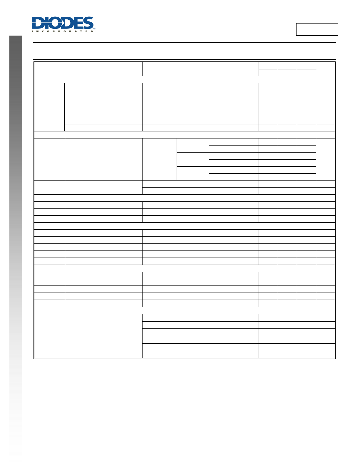
Electrical Characteristics (cont.) (Specifications apply over V
values @TA = +25°C, unless otherwise specified.)
CNTL
= 5V, V
= 1.8V, V
IN
P7176B
= 1.2V and TA = -40°C to +85°C, typical
OUT
Symbol Parameter Conditions
AP7176B
Min Typ Max
OUTPUT VOLTAGE
Reference Voltage FB=V
Output Voltage Accuracy
V
REF
Load Regulation I
V
T
Line Regulation I
V
Pull-low Resistance V
OUT
— 0.8 — V
OUT
= 3.0 ~ 5.5V, I
CNTL
= -40 to +125°C
J
=0A to 3A — 0.06 0.25 %
OUT
=10mA, V
OUT
= 3.3V, VEN = 0V, V
CNTL
CNTL
= 0~3A,
OUT
-1.5 — +1.5 %
= 3.0 to 5.5V -0.15 — +0.15 %/V
<0.8V — 10 —
OUT
FB Input Current VFB = 0.8V -100 — +100 nA
DROPOUT VOLTAGE
T
= 25°C — 0.33 0.38
J
TJ = -40°C to +125°C — 0.53
T
= +25°C — 0.31 0.36
J
TJ = -40°C to +125°C — 0.50
T
= +25°C — 0.30 0.35
J
TJ = -40°C to +125°C — — 0.48
4.5 5.7 6.7 A
NOMINAL
NEW PRODUCT
-to-V
V
IN
(Note 5)
V
DROP
I
Current-Limit Level
LIM
Dropout Voltage
OUT
= 2.5V
V
OUT
= 5.0V,
V
CNTL
= 3A
I
OUT
T
= +25°C, V
J
V
OUT
V
OUT
= 80% V
OUT
= 1.8V
= 1.2V
TJ = -40°C to +125°C 4.2 — — A
PROTECTIONS
I
Short Current-Limit Level VFB < 0.2V — 1.1 — A
SHORT
TSD Thermal Shutdown Temperature TJ rising — 170 — °C
Thermal Shutdown Hysteresis — 50 — °C
ENABLE AND SOFT-START
EN Logic High Threshold Voltage VEN rising 0.5 0.8 1.1 V
EN Hysteresis — 0.1 — V
EN Pull-High Current EN = GND — 5 — µA
TSS Soft-Start Interval 0.3 0.6 1.2 ms
Turn On Delay From being enabled to V
rising 10% 200 350 500 µs
OUT
POWER-GOOD AND DELAY
V
Rising PG Threshold Voltage VFB rising 90 92 95 %
THPG
PG Threshold Hysteresis — 8 — %
PG Pull-low Voltage PG sinks 5mA — 0.25 0.4 V
PG Debounce Interval V
PG Delay Time From VFB = V
< falling PG voltage threshold — 10 — µs
FB
to rising edge of the VPG 1 2 4 ms
THPG
THERMAL CHARACTERISTIC
SO-8EP (Note 6) — 70 —
MSOP-8EP (Note 7) — 80 —
U-DFN3030-10 (Note 6) — 60 —
SO-8EP (Note 6) —
30 —
MSOP-8EP (Note 7) — 30 —
JA
JC
Thermal Resistance Junction-toAmbient
Thermal Resistance Junction-toAmbient
U-DFN3030-10 (Note 6) — 20 —
Notes: 5. Dropout voltage is the voltage difference between the input and the output at which the output voltage drops 2% below its nominal value.
6. Device mounted on 2"*2" FR-4 substrate PC board, 2oz copper, with minimum recommended pad on top layer and thermal vias to bottom layer ground
plane.
7. Device mounted on 2"*2" FR-4 substrate PC board, 2oz copper,with minimum recommended pad layout.
AP7176B
Document number: DS35818 Rev.3 - 2
4 of 14
www.diodes.com
Unit
V
°C/W
°C/W
°C/W
°C/W
°C/W
°C/W
April 2014
© Diodes Incorporated
A
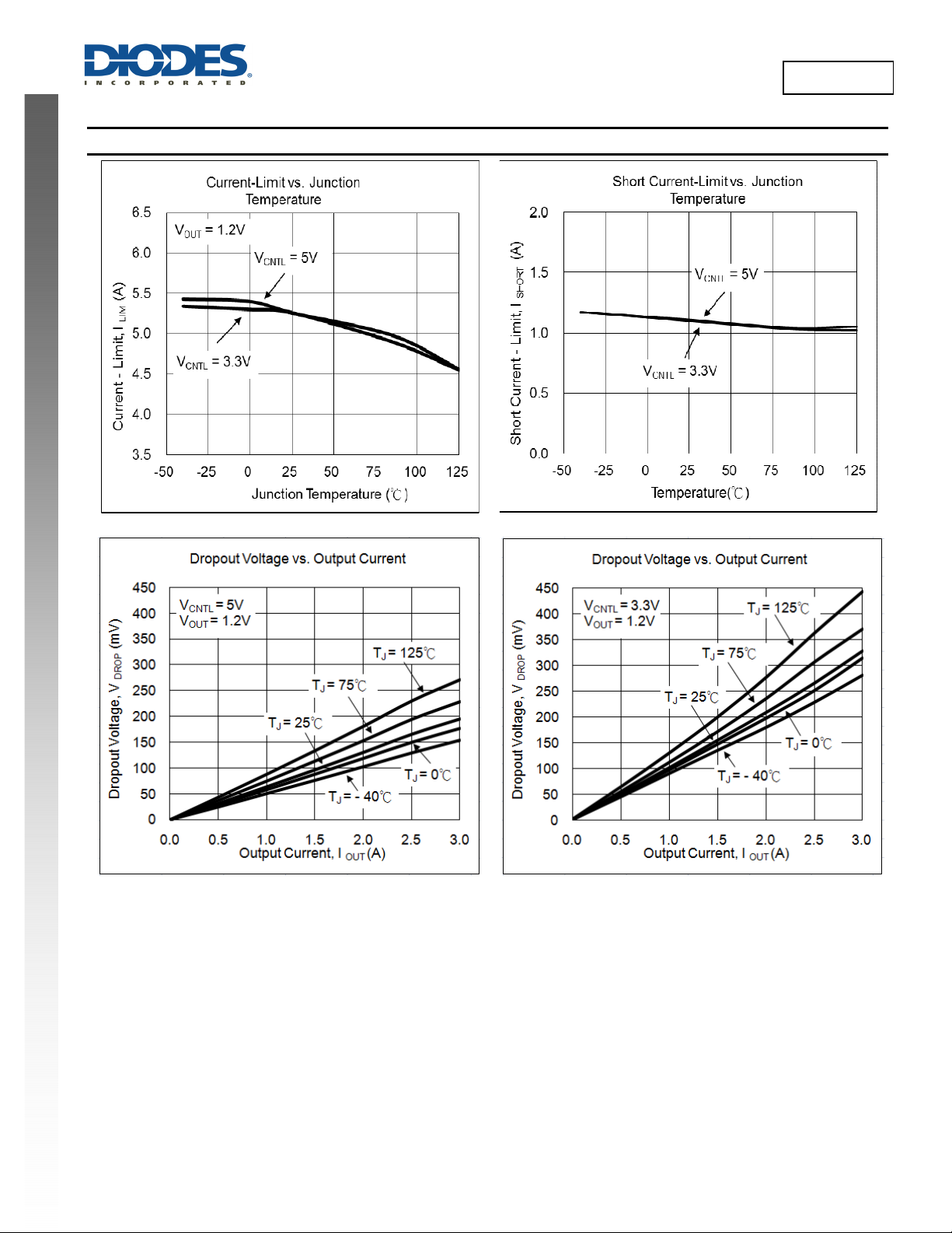
Typical Characteristics
P7176B
NEW PRODUCT
AP7176B
Document number: DS35818 Rev.3 - 2
5 of 14
www.diodes.com
© Diodes Incorporated
April 2014
 Loading...