

Page 1
AP7115
150mA LOW DROPOUT LINEAR REGULATOR WITH
SHUTDOWN
Features
• Wide input voltage range from 2.5V to 5.5V
• 200mV low dropout voltage at 150mA output current
• Guaranteed 150mA output current.
• Low quiescent current 50µA
• Output voltage from 1.0V to 3.5V
• ±2% output voltage accuracy
• Low temperature drift at output voltage
• High PSRR
• Fast transient response
• Current limit protection
• Short circuit protection
• Thermal shutdown protection
• SOT25 and SOT353: Available in “Green” Molding
Compound (No Br, Sb)
• Lead Free Finish/RoHS Compliant (Note 1)
Applications
• Wireless Communication
• GSM/GPRS Cellular Phones
• Handheld Mobile Device s
• Battery Powered Devices
• CD-ROM, DVD, and LAN Cards
• PC and Notebook Peripherals
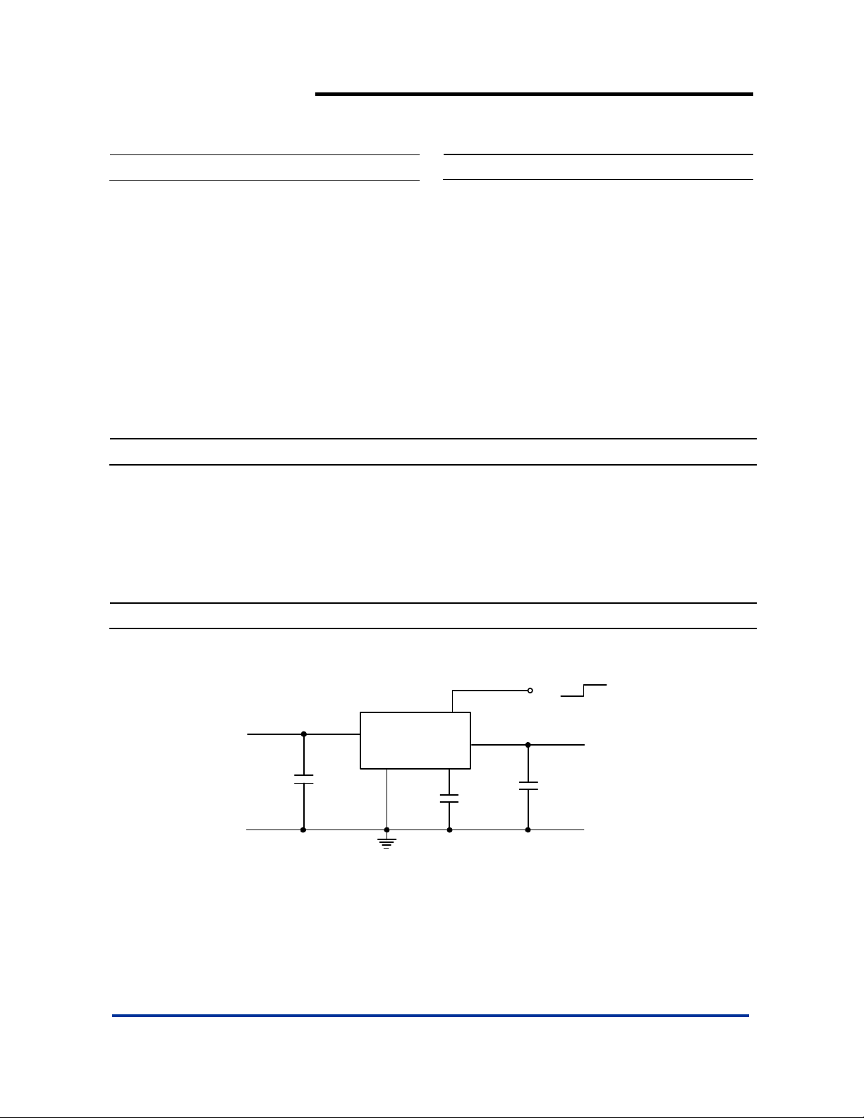
Typical Application Circuit
V
IN
C
IN
1µF
AP7115
IN
GND
General Description
The AP7115 is a 150mA, fixed output voltage, low dropout linear
regulator. The device includes pass element, error amplifier,
band gap reference, current-limit and thermal shutdown circuit.
The characteristics of low dropout voltage and low quiescent
current make it suitable for use in battery powered devices. The
typical quiescent current is approximately 50µA. Several fixed
output voltages are available from 1.0V to 3.5V. Additional
protection is provided with built-in current-limit and
thermal-shutdown functions.
ON
EN
OFF
EN
OUT
BP
C
BP
0.1µF
C
V
OUT
OUT
1µF
AP7115 Rev. 10 1 of 11 MAY 2009
www.diodes.com © Diodes Incorporated
Page 2
Ordering Information
AP7115
150mA LOW DROPOUT LINEAR REGULATOR WITH
SHUTDOWN
AP7115 - XX XX G - 7
Green
G : Green
Packing
7 : Tape & Reel
7” Tape and Reel
Quantity Part Number Suffix
Device
Output voltage Package
10 : 1.0V
12 : 1.2V
15 : 1.5V
18 : 1.8V
25 : 2.5V
28 : 2.8V
29 : 2.85V
30 : 3.0V
33 : 3.3V
35 : 3.5V
Package
Code
W : SOT25
SE : SOT353
Packaging
(Note 2)
AP7115-XXWG-7 W SOT25 3000/Tape & Reel -7
AP7115-XXSEG-7 SE SOT353 3000/Tape & Reel -7
Notes: 1. EU Directive 2002/95/EC (RoHS). All applicable RoHS exemptions applied. Please visit our website at
http://www.diodes.com/products/lead_free.html
2. Pad layout as shown on Diodes Inc. suggested pad layout document AP02001, which can be found on our website at
http://www.diodes.com/datasheets/ap02001.pdf.
.
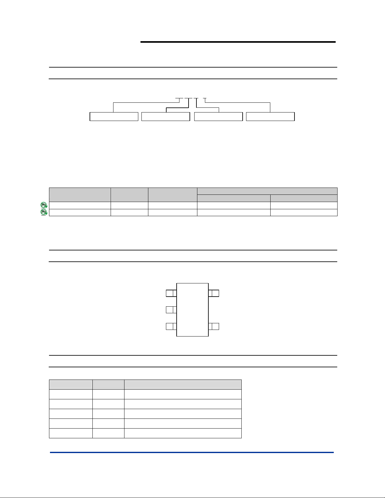
Pin Assignments
( Top View )
IN
1
5
OUT
2
GND
EN
SOT25 / SOT353
43
BP
Pin Descriptions
Pin Name
IN
GND
EN
BP
OUT
Pin NO.
1
2
3
4
5
Voltage Input
Ground
Chip Enable Control
Band-Gap Bypass
Voltage Output
AP7115 Rev. 10 2 of 11 MAY 2009
Description
www.diodes.com © Diodes Incorporated
Page 3
Block Diagram
AP7115
150mA LOW DROPOUT LINEAR REGULATOR WITH
SHUTDOWN
IN
EN
Current
Limit
Enable
-
+
Bandgap
Error
Amp
0.8V
OUT
Thermal
Shutdown
BP
GND
Absolute Maximum Ratings
Symbol Parameter Rating Unit
ESD HBM Human Body Model ESD Protection
ESD MM Machine Model ESD Protection 400 V
VIN Input Voltage -0.3~5.5 V
VCE CE Pin Voltage -0.3~5.5 V
V
Output Voltage -0.3~Vin+0.3 V
OUT
VBP Band Gap Bypass Pin Voltage -0.3~5.5 V
PD Power Dissipation 500 mW
TJ Operating Junction Temperature Range -40 to +125
TST Storage Temperature Ran ge -65 to +150
3.5
KV
o
C
o
C
Recommended Operating Conditions
Symbol Parameter Min Max Unit
VIN Input Voltage 2.5 5.5 V
I
Output Current - 150 mA
OUT
TA Operating Ambient Temperature -40 85
AP7115 Rev. 10 3 of 11 MAY 2009
www.diodes.com © Diodes Incorporated
o
C
Page 4
AP7115
150mA LOW DROPOUT LINEAR REGULATOR WITH
SHUTDOWN
Electrical Characteristics (V
= 3.3V, IL = 30mA, C
CC
= 1μF, C
IN
= 1μF, TA = 25oC)
OUT
Symbol Parameter Conditions Min Typ. Max Unit
System Supply Input
VIN Operating input voltage IL= 0 ~ 150mA 2.5 5.5 V
= V
ΔV
OUT/VOUT
Output Voltage Accu racy
V
IN
1mA ≤ I
+ 1V where
OUT
≤ 50mA
OUT
-2 2 %
VDO Dropout Voltage IL= 150mA 200 300 mV
I
Output Current V
OUT
IQ Quiescent Current
I
Shutdown Current
shutdown
PSRR Power Supply Rejection Ratio I
I
Current Limit 200 250 mA
limit
Thermal Management
T
Thermal Shutdown 150
shutdown
- V
= 1V 150 mA
OUT
= V
+ 1V where
OUT
= 0 and VCE= VIN
= V
+ 1V where
OUT
= 0 and VCE= 0
50 80
0.1 1
= 30mA, f = 1kHz 70 dB
V
I
OUT
V
I
OUT
OUT
IN
IN
IN
µA
µA
o
C
Reference Voltage
ΔV
ΔV
REF
OUT
Tempco of Bandgap Refe rence 30 50
/ΔT
= 30mA, -40℃ ≤ T ≤ 85℃
Tempco of Output Voltage
/ΔT
I
OUT
50 100
ppm/
ppm/
Control and Protection
V
2.0 V
IH,CE
V
0.7 V
IL,CE
ICE CE Pin Leakage Current
V
= V
CE
V
= V
CE
= 5.0V and VSS= 0V 0.01 0.1
IN @VIN
SS @VIN
= 5.0V and V
= 0V 0.01 0.1
SS
µA
µA
Regulation
V
+ 0.5V ≤ VIN ≤ 5.5V where
ΔVO/ΔVIN
ΔV
LOAD
Line Regulation
Load Regulation
OUT
>2.0V, I
V
OUT
1mA ≤ I
V
= V
IN
= 30mA
OUT
≤ 150mA where
L
+ 1V
OUT
0.02 0.1 %/V
0.003 0.006 %/mA
Noise
e
Output Noise BW = 10Hz ~ 100kHz 50
n
Thermal Resistance
θ
θ
Notes: 3. Test condition for SOT25 and SOT353: Device mounted on FR-4 substrate PC board, 2oz copper, with minimum recommended pad layout.
Thermal Resistance
JA
Junction-to-Ambient
Thermal Resistance
JC
Junction-to-Case
SOT25 (Note 3) - 200 SOT353 (Note 3) 337
SOT25 (Note 3) - 52 SOT353 (Note 3) 121
µV
o
C/W
o
C/W
o
C/W
o
C/W
rms
o
C
o
C
AP7115 Rev. 10 4 of 11 MAY 2009
www.diodes.com © Diodes Incorporated
Page 5

150mA LOW DROPOUT LINEAR REGULATOR WITH
Typical Operating Characteristics
AP7115
SHUTDOWN
Qui esce n t cu r ren t vs. V cc
( V
=2.5~5.5V, I
IN
80
70
60
50
40
30
Qu iescen t current (uA)
20
2.5V 3.0V 3.5V 4.0V 4.5V 5.0V 5.5V
OUT
=0mA )
Vcc
Current limit vs. Te m perature
( V
=2.5V, V
270
250
230
210
190
Current limit (mA)
170
150
-40℃ -20℃ 0℃ 25℃ 50℃ 85℃
IN
Temper ature
OUT
=1.0V )
Qu iescen t cu rrent vs. Temperature
( V
=5V, I
IN
80
70
60
50
40
30
Quiescent current (uA)
20
-40℃ -20℃ 0℃ 25℃ 50℃ 85℃
=0mA )
OUT
Temperature
Current limit vs. Temperature
=5V, V
( V
330
310
290
270
250
230
210
190
Current limit (mA)
170
150
-40℃ -20℃ 0℃ 25℃ 50℃ 85℃
IN
=1.0V )
OUT
Tempe rature
Iout vs. Dropout voltage
=25℃ )
( T
250
200
150
100
50
Dropout voltage (mV)
0
0mA 20mA 40m A 60mA 80mA 100m A 120mA 150mA
A
Iout
370
320
270
220
170
Cur ren t limit (mA)
120
Current limit vs. Input voltage
=25℃ )
( T
A
2.5V 3.0V 3. 5V 4. 0V 4.5V 5.0V 5. 5V
Input voltage
AP7115 Rev. 10 5 of 11 MAY 2009
www.diodes.com © Diodes Incorporated
Page 6

150mA LOW DROPOUT LINEAR REGULATOR WITH
Typical Operating Characteristics (Continued)
AP7115
SHUTDOWN
Short current vs. Temperature
( V
=2.5V)
68
65
62
59
56
Sho rt current (mA)
53
50
-40℃ -20℃ 0℃ 25℃ 50℃ 85℃
IN
Temperature
Output Noise Output Noise
Short current vs. Temperature
( V
=5V )
74
71
68
65
62
59
56
Shor t current (mA)
53
50
-40℃ -20℃ 0℃ 25℃ 50℃ 85℃
IN
Temper ature
Output Noise
AP7115 Rev. 10 6 of 11 MAY 2009
www.diodes.com © Diodes Incorporated
Page 7

150mA LOW DROPOUT LINEAR REGULATOR WITH
Typical Operating Characteristics (Continued)
Load Transient Response Load Transient Response
AP7115
SHUTDOWN
Start Up (EN vs. V
Start Up (EN vs. V
) Start Up (EN vs. V
OUT
) Start Up (EN vs. V
OUT
)
OUT
)
OUT
AP7115 Rev. 10 7 of 11 MAY 2009
www.diodes.com © Diodes Incorporated
Page 8

150mA LOW DROPOUT LINEAR REGULATOR WITH
Application Note
Input Capacitor
An 1uF input capacitor is required between the AP7115 input pin
and GND.
There are no requirements for the ESR on input capacitor, but
tolerance and temperature coefficient must be considered.
Output Capacitor
The AP7115 can work with very small ceramic output capacitors
(1uF or greater). Higher capacitance values help to improve
transient. The output capacitor’s ESR is critical because it from a
zero to provide phase lead which is required for loop stability.
Figure below is Cout ESR vs. Load Current.
AP7115 Region of Stable Cout ESR vs.
Load Current
100
10
AP7115
SHUTDOWN
PCB Layout
Optimum performance can only be achieved when the device is
mounted on a PC board according to the diagram below:
1
Stable
0.1
Cout ESR (Ω)
0.01
0 20 40 60 80 100 120 140 160
Load Current (mA)
Band-Gap Bypass Capacitor
0.1uF bypass capacitor Between BP pin and GND can reduces
output voltage noise.
Shutdown Input Operation
The AP7115 is shutdown by pulling the EN pin low, and turned on
by driving the input high. If the shutdown feature is not required,
the EN pin should be tied to VIN to keep the regulator on at all
times.
Dropout Voltage
V
DROPOUT=VIN-VOUT=RDS(ON)×IOUT
Current Limit
The AP7115 monitors and controls the PMOS’ gate voltage,
limiting the output current to 250mA(typ.). The output can be
shorted to ground for an indefinite period of time without
damaging the part.
Thermal Considerations
Thermal Shutdown Protection limits power dissipati on in A P7115 .
When the operation junction temperature exceeds 155°C, the
Over Temperature Protection circuit starts the thermal shutdown
function and turns the pass element off. The pass element turn
on again after the junction temperature cools by 30°C. For
continuous operation, do not exceed absolute maximum
operation junction temperature 125°C. The power dissipation
definition in device is:
PD = (VIN − V
The maximum power dissipation depends on the thermal
resistance of IC package, PCB layout, the rate of surroundings
airflow and temperature difference between junction to ambient.
The maximum power dissipation can be calculated by the
following formula:
P
= ( T
D(MAX)
Where T
125°C, T
to ambient thermal resistance.
J(MAX)
is the ambient temperature and the θJA is the junction
A
) x I
OUT
J(MAX)
is the maximum operation junction temperature
+ VIN x IQ
OUT
- TA ) / θJA
AP7115 Rev. 10 8 of 11 MAY 2009
www.diodes.com © Diodes Incorporated
Page 9

r
r
Marking Information
AP7115
150mA LOW DROPOUT LINEAR REGULATOR WITH
SHUTDOWN
( Top View )
5
7
4
XX : Identification code
Y
: Year 0~9
XX
W X
Y
: Week : A~Z : 1~26 week;
W
a~z : 27~52 week; z represents
52 and 53 week
: A~Z : Green
1 2 3
Part Numbe
SOT25 SOT353
AP7115-10W FO AP7115-10SE GO
AP7115-12W FP AP7115-12SE GP
AP7115-15W FQ AP7115-15SE GQ
AP7115-18W FR AP7115-18SE GR
AP7115-25W FS AP7115-25SE GS
AP7115-28W FT AP7115-28SE GT
AP7115-29W FU AP7115-29SE GU
AP7115-30W FV AP7115-30SE GV
AP7115-33W FW AP7115-33SE GW
AP7115-35W FX AP7115-35SE GX
AP7115 Rev. 10 9 of 11 MAY 2009
Identification Code
www.diodes.com © Diodes Incorporated
X
Part Numbe
Identification Code
Page 10

150mA LOW DROPOUT LINEAR REGULATOR WITH
Package Information (All Dimensions in mm)
(1) Package Type: SOT25
AP7115
SHUTDOWN
(2) Package Type: SOT353
2.0/2.2
1.15/ 1.35
1.8/2.2
1.10M ax.
0/0.1 0.9/ 1.0
0.10/0.30
C
L
0.65Bsc.
0.1/0.22
DETAIL"A"
C
L
Gauge Plane
0.25/ 0.40
"A"
AP7115 Rev. 10 10 of 11 MAY 2009
www.diodes.com © Diodes Incorporated
Page 11

AP7115
150mA LOW DROPOUT LINEAR REGULATOR WITH
SHUTDOWN
DIODES INCORPORATED MAKES NO WARRANTY OF ANY KIND, EXPRESS OR IMPLIED, WITH REGARDS TO THIS
DOCUMENT, INCLUDING, BUT NOT LIMITED TO, THE IMPLIED WARRANTIES OF MERCHANTABILITY AND FITNESS FOR A
PARTICULAR PURPOSE (AND THEIR EQUIVALENTS UNDER THE LAWS OF ANY JURISDICTION).
Diodes Incorporated and its subs idiaries reserve the right to make modific ations, enhancem ents, improvem ents, correctio ns or other
changes without further notic e to this document and any product des cri bed herein. Diodes Inc orporat ed does not assum e any liabi lity
arising out of the applicati on or use of this document or any produc t described herein ; neither does Diodes In corporat ed convey any
license under its patent or trademark rights, nor the rights of others . Any Customer or user of t his document or produc ts described
herein in such applications shall assume all risks of such use and will agree to hold Diodes Incorporated and all the companies
whose products are represented on Diodes Incorporated website, harmless against all damages.
Diodes Incorporated do es not warrant or accept an y liabilit y whatsoever in re spect of any product s purchased through unaut horized
sales channel.
Should Customers purchase or use Diod es Incorporated products for any unintend ed or unauthorized application, Custom ers shall
indemnify and hold Diodes Incorpor ated and its repres entatives harmless agai nst all claims, damages , expenses, and atto rney fees
arising out of, directly or indi re ct l y, any c l a im of person al i nj u ry or death ass oci a t e d with suc h uni nte nde d or un authorized application.
Products described h erein may be covered by one or more United States, i nternational or f oreign patents pendi ng. Product names
and markings noted herein may also be covered by one or more Uni ted S tates, international or foreign tradem a rks.
Diodes Incorporated products are specific ally not authorized for use as critical components in life support devic es or systems without
the express written approval of t he Chief Execut ive Officer of Diodes Incorporated. As used herei n :
A. Life support devices or systems are devices or systems which:
1. are intended to implant into the body, or
2. support or sustain life and whose failure to perform when properly used in accordance with ins t ruc t i ons for use provided
in the labeling can be reasonably expected to result in significant injury to the user.
B. A critical component is any component in a life support device or syst em whose failu re to perform can be rea sonably expect ed
to cause the failure of the life support device or to affect its safety or effectiveness.
Customers represent that they have all nec essary expertise in the safet y and regulatory ramificati ons of their life support devices or
systems, and acknowledge and agree that they are solely responsible for all legal, regulatory and safety-related requirements
concerning their products and any use of Diodes Incorporated products in such safety-critical, life support devices or systems,
notwithstanding any devices- or systems-related information or support that may be provided by Diodes Incorporated. Further,
Customers must fully indemnif y Diodes Incorporated and its representati ves against any damages arising out of the use of Diodes
Incorporated products in such safety-critical, life support devices or systems.
Copyright © 2009, Diodes Incorporated
www.diodes.com
IMPORTANT NOTICE
LIFE SUPPORT
AP7115 Rev. 10 11 of 11 MAY 2009
www.diodes.com © Diodes Incorporated
 Loading...