

Page 1
AP63200/AP63201/AP63203/AP63205
is a 2A, synchronous
range of 3.8V to 32V and
down DC/DC
easily used by
minimizing the external component count due to its adoption of peak
The AP63200/AP63201/AP63203/AP63205 has optimized designs for
tion. The converter features
Frequency Spread Spectrum (FSS) with a switching frequency jitter of
reduces EMI by not allowing emitted energy to stay in any
It also has a proprietary
without sacrificing
• Halogen and Antimony Free. “Green” Device (Note 3)
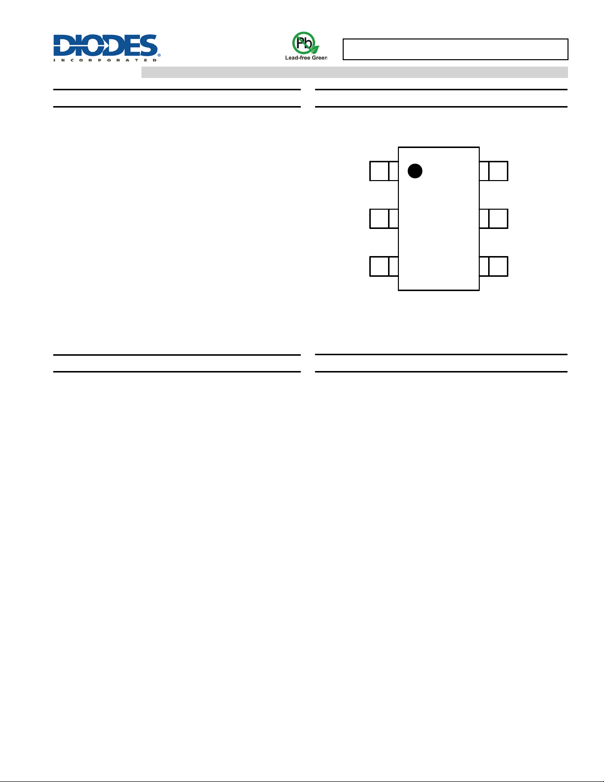
1
2
3 4
5
6
FB
EN
VIN GND
SW
BST
TSOT26
TOP VIEW
3.8V TO 32V INPUT, 2A LOW IQ SYNCHRONOUS BUCK WITH ENHANCED EMI REDUCTION
Description
The AP63200/AP63201/AP63203/AP63205
buck converter with a wide input voltage
fully integrates a 125mΩ high-side power MOSFET and a 68mΩ lowside power MOSFET to provide high-efficiency stepconversion.
The AP63200/AP63201/AP63203/AP63205 device is
Pin Assignments
current mode control along with its integrated compensation network.
Electromagnetic Interference (EMI) reduc
±6%, which
one frequency for a significant period of time.
gate driver scheme to resist switching node ringing
MOSFET turn-on and turn-off times, which further erases highfrequency radiated EMI noise caused by MOSFET switching.
The device is available in a low-profile, TSOT26 package.
Features
• VIN 3.8V to 32V
• 2A Continuous Output Current
• 0.8V ± 1% Reference Voltage
• 22µA Ultralow Quiescent Current
• Switching Frequency
o 500kHz: AP63200 and AP63201
o 1.1MHz: AP63203 and AP63205
• Pulse Width Modulation (PWM) Regardless of Output Load
o AP63201
• Supports Pulse Frequency Modulation (PFM)
o AP63200, AP63203, and AP63205
o Up to 80% Efficiency at 1mA Light Load
o Up to 88% Efficiency at 5mA Light Load
• Fixed Output Voltage
o 3.3V: AP63203
o 5.0V: AP63205
• Proprietary Gate Driver Design for Best EMI Reduction
• Frequency Spread Spectrum (FSS) to Reduce EMI
• Precision Enable Threshold to Adjus t UVLO
• Protection Circuitry
o Overvoltage Protection
o Cycle-by-Cycle Peak Current Limit
o Thermal Shutdown
• Totally Lead-Free & Fully RoHS Compliant (Notes 1 & 2)
Applications
• 12V and 24V Distributed Power Bus Supplies
• Flat Screen TV Sets and Monitors
• Power Tools and Laser Printers
• White Goods and Small Home Appliances
• FPGA, DSP, and ASIC Supplies
• Home Audio
• Network Systems
• Set Top Boxes
• Gaming Consoles
• Consumer Electronics
Notes: 1. No purposely added lead. Fully EU Directive 2002/95/EC (RoHS), 2011/65/EU (RoHS 2) & 2015/863/EU (RoHS 3) compliant.
2. See https://www.diodes.com/quality/lead-free/ for more information about Diodes Incorporated’s definitions of Halogen- and Antimony-free, "Green" and
3. Halogen- and Antimony-free "Green” products are defined as those which contain <900ppm bromine, <900ppm chlorine (<1500ppm total Br + Cl) and
Lead-free.
<1000ppm antimony compounds.
AP63200/AP63201/AP63203/AP63205
Document number: DS41326 Rev. 2 - 2
1 of 18
www.diodes.com
January 2019
© Diodes Incorporated
Page 2
AP63200/AP63201/AP63203/AP63205
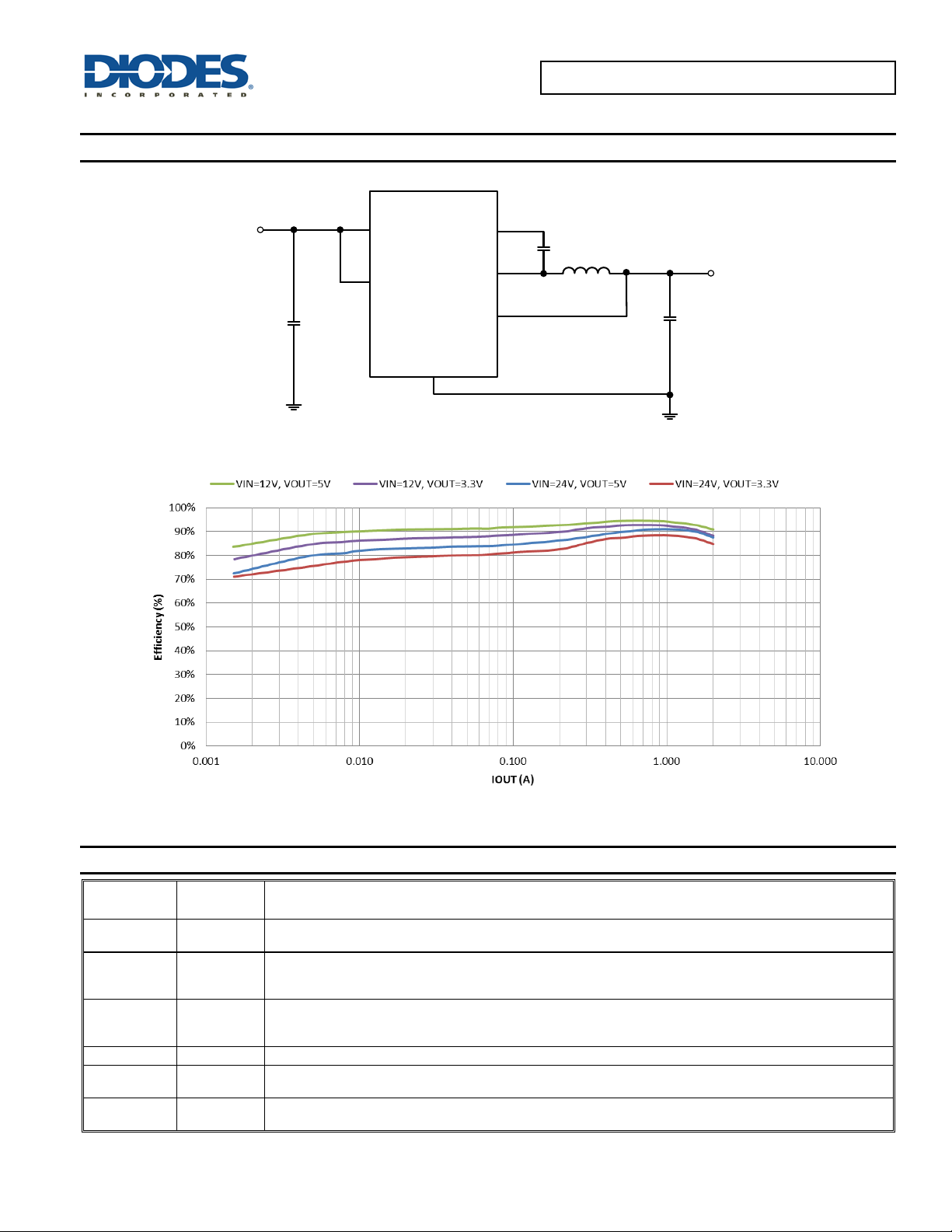
AP63205
L
4.7µH
C3
100nF
C2
2x22μF
C1
10μF
3
VIN
2
EN
5
SW
6
BST
1
FB
4
GND
OUTPUT
V
OUT
5V
INPUT
Feedback sensing terminal for the output voltage. Connect this pin to the resistive divider of the output.
Setting the Output Voltage
programing the UVLO. See Enable section for more details.
Power Input. VIN suppli es the power to the IC, as well as the step-down converter switches. Drive VIN wi th a
switching of the IC. See Input Capacitor section for more details.
4
GND
Power Ground.
Power Switching Output. SW is the switching node that supplies power to the output. Connect the output LC filter
from SW to the output load. Note that a capacitor is required from SW to BST to power the high-side switch.
High-Side Gate Drive Boost Input. BST supplies the drive for the high-side N-Channel MOSFET. A 100nF
Typical Application Circuit
Figure 1. Typical Application Circuit
Figure 2. Efficiency vs. Output Current
Pin Descriptions
Pin Number Pin Name Function
1 FB
2 EN
AP63200/AP63201/AP63203/AP63205
Document number: DS41326 Rev. 2 - 2
3 VIN
5 SW
6 BST
See
section for more details.
Enable Input. EN is a digital input that turns the regulator on or off. Drive EN high to turn on the regulator and low
to turn it off. Attach to VIN or leave open f or automatic startup. The EN has a precision threshold of 1.18V f or
3.8V to 32V power source. Bypass VIN t o GND with a suitably large capacitor to eliminate noise due to the
capacitor is recommended from SW to BST to power the high-side switch.
2 of 18
www.diodes.com
January 2019
© Diodes Incorporated
Page 3
AP63200/AP63201/AP63203/AP63205
0.4V
0.8V
1.1V
+
-
+
-
-
+
0.6V
+
0.8V
Inte rna l SS
Error
Amplifier
PWM
Comparator
Oscillator
+
Logic
-
+
Ref
OCP
7.6nF
18kΩ
SE = 0.84V/T
RT = 0.2V/A
UVP
Q1
Q2
1
2
EN
FB
4
GND
5
SW
6
BST
3
VIN
gm
20kΩ
+
-
Internal
Reference
VCC
Regulator
ON
1.18V
1.5µA 4µA
VSUM
COMP
CSA
Functional Block Diagram
AP63200/AP63201/AP63203/AP63205
Document number: DS41326 Rev. 2 - 2
Figure 3. Functional Block Diagram
3 of 18
www.diodes.com
January 2019
© Diodes Incorporated
Page 4
AP63200/AP63201/AP63203/AP63205
Symbol
Parameter
Rating
Unit
IN
BST
SW
SW
Feedback Voltage
-0.3V to +6.0
V
VEN
Enable/UVLO Voltage
-0.3V to +35.0
V
TST
TJ
TL
Lead Temperature
+260
°C
ESD Susceptibility (Note 5)
HBM
Human Body Mode
2000
V
CDM
Charge Device Model
1000
V
Symbol
Parameter
Rating
Unit
θ
JA
θ
JC
Symbol
Parameter
Min
Max
Unit
3.8
Operating Ambient Temperature Range
-40
+85
°C
Absolute Maximum Ratings (Note 4) (@T
= +25°C, unless otherwise specified.)
A
VIN
VSW
V
Supply Voltage
Switch Node Voltage
Bootstrap Voltage
-0.3 to +35.0 (DC) V
-0.3 to +40.0 (400ms) V
V
-1.0 to V
- 0.3 to V
+ 0.3
+ 6.0
V
V
VFB
Storage Temperature -65 to +150 °C
Junction Temperature +160 °C
Notes: 4. Stresses greater than the 'Absolute Maximum Ratings' specified above may cause permanent damage to the device. These are stress ratings only;
functional operation of the device at these or any other conditions exceeding those indicated in this specification is not implied. Device reliability may
be affected by exposure to absolute maximum rating conditions for extended periods of time.
5. Semiconductor devices are ESD sensitive and may be damaged by exposure to ESD events. Suitable ESD precautions should be taken when
handling and transporting these devices.
Thermal Resistance (Note 6)
Junction to Ambient TSOT26 89 °C/W
Junction to Case TSOT26 39 °C/W
Note: 6. Test condition for TSOT26: Device mounted on FR-4 substrate, single-layer PC board, 2oz copper, with minimum recommended pad layout.
Recommended Operating Conditions (Note 7) (@T
= +25°C, unless otherwise specified.)
A
VIN
TA
Note: 7. The device function is not guaranteed outside of the recommended operating conditions.
AP63200/AP63201/AP63203/AP63205
Document number: DS41326 Rev. 2 - 2
Supply Voltage
4 of 18
www.diodes.com
32 V
January 2019
© Diodes Incorporated
Page 5
AP63200/AP63201/AP63203/AP63205
Symbol
Parameter
Test Conditions
Min
Typ
Max
Unit
I
SHDN
Shutdown Supply Current
VEN = 0V
— 1 3
µA
AP63201:
VEN = OPEN, VFB = 1.0V
AP63200/AP63203/AP63205:
IN
R
DS(ON)1
High-Side Switch On-Resistance (Note 8)
— — 125 — mΩ
R
DS(ON)2
I
PEAK_LIMIT
I
VALLEY_LIMIT
AP63200/AP63201
—
500 — kHz
AP63203/AP63205
—
1100 — kHz
FSS
Frequency Spread Spectrum
— — ±6 — %
tON
CCM, AP63200/AP63201
792
800
808
mV
CCM, AP63203
3.27
3.30
3.33
V
CCM, AP63205
4.95
5.00
5.05
V
V
EN_H
V
EN_L
VEN = 1.5V
VEN = 1V
—
1.5 — μA
tSS
Soft-Start Period
— — 4 — ms
HYS
Electrical Characteristics (T
ambient temperature range, -40°C to +85°C, and input voltage range, 3.8V to 32V).
IQ
UVLO
Supply Current (Quiescent)
V
Under Voltage Threshold (Rising)
VIN Under Voltage Threshold Hysteresis
Low-Side Switch On-Resistance (Note 8) — — 68 — mΩ
HS Peak Current Limit (Note 8) — 2.5 2.8 3.1 A
LS Valley Current Limit (Note 8) — 2.5 3.2 3.9 A
= +25°C, VIN = 12V, unless otherwise specified. Min/Max limits apply across the recommended
A
VEN = OPEN, VFB = 1.0V
— 3.30 3.50 3.70 V
— — 440 — mV
— 258 — µA
— 22 — µA
fSW
Oscillator Frequency
Minimum On Time — — 80 — ns
VFB
Feedback Voltage
EN Logic High — 1.15 1.18 1.23 V
EN Logic Low — 1.05 1.10 1.15 V
IEN
TSD
T
Note: 8. Compliance to the datasheet limits is assured by one or more methods: production test, characterization, and/or design.
EN Input Current
Thermal Shutdown (Note 8) — — +160 — °C
Thermal Hysteresis (Note 8) — — +25 — °C
— 5.5 — μA
AP63200/AP63201/AP63203/AP63205
Document number: DS41326 Rev. 2 - 2
5 of 18
www.diodes.com
January 2019
© Diodes Incorporated
Page 6

AP63200/AP63201/AP63203/AP63205
Figure 4. Efficiency vs. Output Current, VIN = 12V
Figure 5. Efficiency vs. Output Current, VIN = 24V
Figure 6. Load Regulation, VOUT = 5V
Figure 7. Line Regulation, VOUT = 5V
Figure 8. Feedback Voltage vs. Temperature
Figure 9. Power Switch R
vs. Temperature
Typical Performance Characteristics (AP63200 @T
= +25°C, VIN = 12V, V
A
= 5V, unless otherwise specified.)
OUT
AP63200/AP63201/AP63203/AP63205
Document number: DS41326 Rev. 2 - 2
www.diodes.com
6 of 18
DS(ON)
January 2019
© Diodes Incorporated
Page 7

AP63200/AP63201/AP63203/AP63205
Figure 10. IQ vs. Temperature
Figure 11. I
vs. Temperature
Figure 12. F
vs. Temperature
Figure 13. VIN POR and UVLO vs. Temperature
Figure 14. Startup using EN, Iout = 2A
Figure 15. Shutdown using EN, Iout = 2A
EN (5V/div)
VOUT (2V/div)
I
(2A/div)
SW (10V/div)
2ms/div
EN (5V/div)
VOUT (2V/div)
I
(2A/div)
SW (10V/div)
50µs/div
Typical Performance Characteristics (continued)
SHDN
SW
AP63200/AP63201/AP63203/AP63205
Document number: DS41326 Rev. 2 - 2
www.diodes.com
7 of 18
January 2019
© Diodes Incorporated
Page 8

AP63200/AP63201/AP63203/AP63205
Figure 16. Output Ripple, Iout = 2A
Figure 17. Load Transient, Iout = 1A to 2A
Figure 18. Output Short Protect i on, Iout = 2A
Figure 19. Output Short Recovery, Iout = 2A
V
Ripple (20mV/div)
I
(1A/div)
SW (10V/div)
2µs/div
V
Ripple (500mV/div)
I
(1A/div)
1ms/div
V
(2V/div)
I
(2A/div)
SW (10V/div)
10ms/div
V
(2V/div)
I
(2A/div)
SW (10V/div)
10ms/div
Typical Performance Characteristics (continued)
AP63200/AP63201/AP63203/AP63205
Document number: DS41326 Rev. 2 - 2
www.diodes.com
8 of 18
January 2019
© Diodes Incorporated
Page 9

AP63200/AP63201/AP63203/AP63205
AP
63200
AP63201
L
2.2μH
R
1
30.9kΩ
R2
62kΩ
C3
100nF
C2
2x22μF
C1
10μF
3
VIN
2
EN
5
SW
6
BST
1
FB
4
GND
OUTPUT
V
OUT
1.2V
INPUT
C
4
100pF
AP63203
AP63205
L
C3
100nF
C2
2x22μF
C1
10μF
3
VIN
2
EN
5
SW
6
BST
1
FB
4
GND
OUTPUT
V
OUT
INPUT
Application Information
Figure 20. Typical Application Circuit of AP63200/AP63201
Figure 21. Typical Application Circuit of AP63203/AP63205
1 PWM Operation Control
The AP63200/AP63201/AP63203/AP63205 device is a 3.8V-to-32V input, 2A output, EMI friendly, fully integrated synchronous buck converter.
Refer to the block diagram in Figure 3. The device employs fixed-frequency peak current mode control. The int ernal clock’s rising edge (500kHz for
AP6300 and AP63201, 1.1MHz for AP63203 and AP63205) initiates turning on the integrated high-side power MOSFET, Q1, for each cycle. W hen
Q1 is on, the inductor current rises linearly, and the device charges the output capacitor. The current across Q1 is sensed and converted to a
voltage with a ratio of R
via the CSA block. The CSA output is combined with an internal slope compensation, SE, resulting in V
T
rises higher than the internal COMP node, the device turns off Q1 and turns on t he low-side power MOSFET, Q2. The inductor current decreas es
when Q2 is on. On the rising edge of next clock cycle, Q2 turns off, and Q1 turns on. This sequence repeats every clock cycle.
The peak current mode control with the internal loop compensation network and built-in 4ms soft-start simplifies the
AP63200/AP63201/AP63203/AP63205 footprint as well as minimizes the external component count.
The error amplifier generates the COMP voltage by c omparing t he voltage on t he FB pin with an internal 0. 8V ref erenc e. A n inc rease in load current
causes the feedback voltage to drop. The error amplifier thus raises the COMP voltage until t he average inductor current matches the increased
load current. This feedback loop regulates the output voltage. The device also integrates internal slope compensation circuitry to prevent
subharmonic oscillation when the duty cycle is greater than 50% for peak current mode control.
The AP63200/AP63201/AP63203/AP63205 device implements Frequency Spread Spectrum (FSS) with a switching frequency jitter of ±6%. FSS
reduces EMI by not allowing emitted energy to stay in any one frequency for a signific ant period of time. The converter further dampens high
frequency radiated EMI noise through the use of its proprietary gate driver scheme to achieve a ringing-free switching node voltage without
sacrificing the MOSFET switching times.
AP63200/AP63201/AP63203/AP63205
Document number: DS41326 Rev. 2 - 2
. When V
SUM
9 of 18
www.diodes.com
January 2019
© Diodes Incorporated
SUM
Page 10

AP63200/AP63201/AP63203/AP63205
EN
20kΩ
+
-
ON
1.18V
I
1
1.5
µA
I
2
4µA
VIN
R5
R6
2
=
.
.
=
.
. + .
Application Information (continued)
In order to provide a small output ripple in light load conditions, t he AP63201 offers a fixed 500kHz switching f requency with FSS and Pulse Width
Modulation (PWM).
The hiccup mode minimizes power dissipation during prolonged output overcurrent or short c onditions. The hiccup wait time is 512 cycles and the
hiccup restart time is 8192 cycles. The AP63200/AP63201/AP63203/AP63205 also features full protections including cycle-by-cycle high-side
MOSFET peak current limit, overvoltage protection, and overtemperature protection.
2 Pulse Frequency Modulation
In heavy load conditions, the AP63200, AP63203, and AP63205 operate at forced PWM mode. The internal COMP node voltage decreases as the
load current decreases. At a certain limit, if the load current is l ow enough, the COMP node voltage is c lamped and is prevented from decreasing
any further. The voltage at which COMP is c lamped corresponds to the 450mA peak inductor current. As the load current approaches zero, the
AP63200, AP63203, and AP63205 enter Pulse Frequency Modulation (PFM) to increase the converter power efficiency at light load conditions. The
AP63201 remains in c ontinuous conduction mode at light load conditions. When the inductor current decreases to zero, zero-cross detection
circuitry on the low-side power MOSFET, Q2, forces it off until t he beginning of the next switching cycle. The buck converter does not sink c urrent
from the output when the output load is light and while the device is in PFM. Because the AP63200, AP63203, and AP63205 work in PFM during
light load conditions, they can achieve power efficiency of up to 88% at a 5mA load condition.
The quiescent current of AP63200, AP63203 and AP63205 is 22μA typical under a no-load, non-switching condition.
3 Enable
When disabled, the device shutdown supply current is only 1μA. When applying a voltage higher than the EN upper thres hol d (typical 1.18V, rising),
the AP63200/AP63201/AP63203/AP63205 enables all functions, and the device initiates the soft-start phase. The
AP63200/AP63201/AP63203/AP63205 has a built-in 4ms soft-start time to prevent output voltage overshoot and inrush current. When the EN
voltage falls below its lower threshold (typical 1.1V, falling), the internal SS voltage is discharged to ground and device operat i on is disabled.
An internal 1.5µA pull-up current source connected from the internal LDO-regulated VCC to the EN pin guarantees that a high on the EN pin
automatically enables the device. For applications requiring a higher VIN UVLO voltage than is provided by the default setup, there is a 4µA
hysteresis pull-up current source on the EN pin that configures the VIN UVLO voltage with an external resistive divider (R5 and R6) shown in Figure
22. The resistive divider resistor values are calculated by equations Eq.1 and Eq.2.
Where:
• V
• V
AP63200/AP63201/AP63203/AP63205
Document number: DS41326 Rev. 2 - 2
is the rising edge voltage to enable the regulator
ON
is the falling edge voltage to disable the regulator
OFF
Figure 22. Programming UVLO
10 of 18
www.diodes.com
© Diodes Incorporated
Eq. 1
Eq. 2
January 2019
Page 11

AP63200/AP63201/AP63203/AP63205
[] = . []
Eq. 3
SW (5V/div)
IL (1A/div)
No SW Ringing
2µs/div
Application Information (continued)
Alternatively, a small ceramic capacitor can be added from EN to GND. This delays the output startup voltage, which is useful when sequencing
multiple power rails to minimize input inrush current. The amount of capacitance is calculated by equation Eq.3.
Where:
is the time delay capacitance in nF
• C
d
is the delay time in ms
• t
s
The EN pin is a high voltage pin and can be directly connected to VIN to automatically start up the device as VIN increases.
4 Undervoltage Lockout
Undervoltage lockout is implemented to prevent the IC from insufficient input voltages. The AP63200/AP63201/AP63203/AP63205 device has a
UVLO comparator that monitors the input voltage and the internal bandgap reference. If the input voltage falls below 3.1V, the
AP63200/AP63201/AP63203/AP63205 is disabled. In this event, both the high-side and low-side power MOSFETs are turned off.
5 EMI Reduction with Frequency Spread Spectrum and Ringing-free Switching Node
In the some applications, the system must meet EMI standards. To improve EMI reduction, the AP63200/AP63201/AP63203/AP63205 adopts FSS
to spread the switching noise over a wider frequency band and therefore reduces conducted and radiated interference at a particular frequency.
In buck converters, the switching node’s (SW’s) ringing amplitude and cycles are critical, especially in relation to the high frequency radiation EMI
noise. The AP63200/AP63201/AP63203/AP63205 device implements a multi-level gate driver scheme to achieve a ringing-free switc hing node
without sacrificing neither the switching node’s rise and fall slew rates nor the converter’s power efficiency. The AP63203 and AP63205 also have
the feature to remove the resonance ringing of the SW pin when the inductor current is 0A and the device operates in PFM. The zoomed in
waveform for SW is shown in Figure 23.
6 Overcurrent Protection
The AP63200/AP63201/AP63203/AP63205 has cycle-by-cycle peak current limit protection by sensing the current t hrough the internal high-side
power MOSFET Q1. While Q1 is on, its conduction current is monitored by the internal sensing circuitry. Once the current through Q1 exceeds the
current peak limit, Q1 immediately turns off. If Q1 consistently hits the peak current limit for 2ms, the buck converter enters hiccup mode and shuts
down. After 16ms of off time, the buck converter restarts powering up. Hiccup mode reduces the power dissipation in the overcurrent condition.
7 Thermal Shutdown
If the junction temperature of the device reaches the t herm al shut down limi t of +150°C, the AP63200/AP63201/AP63203/AP63205 shuts down both
their high-side and low-side power MOSFETs. W hen the junction temperature reduces to the required level (+130°C nominal), the device initiates a
normal power-up cycle with soft-start.
AP63200/AP63201/AP63203/AP63205
Document number: DS41326 Rev. 2 - 2
Figure 23. AP63203/AP63205 SW Node Waveform
11 of 18
www.diodes.com
January 2019
© Diodes Incorporated
Page 12

AP63200/AP63201/AP63203/AP63205
= (
)
= +
= (
.
)
Application Information (continued)
8 Power Derating Characteri sti cs
To prevent the regulator from exceeding the maximum junction temperature, some thermal analysis is required. The temperature rise is given by:
Where PD is the power dissipated by the regulator and θ
The junction temperature, T
Where T
exceed the absolute maximum junction temperature of +125°C when considering the thermal design. A typical derating curve versus ambient
temperature is shown in Figure 24.
is the ambient temperature of the environment. For the TSOT26 package, the θ
A
, is given by:
J
is the thermal resistance from the junction of the die to the ambient temperature.
JA
is 89°C/W. The actual junction temperature should not
JA
Eq. 4
Eq. 5
Figure 24. Output Current Derating Curve vs. Temperature, VIN = 12V
9 Setting the Output Voltage
The AP63203 and AP63205 have fixed output voltages of 3.3V and 5V, respectively. The AP63200 and AP63201 have adjustable output
voltages starting from 0. 8V using an external resistive divider. An opti onal in Figure 20, of 10pF to 220pF is used to improve the transient
response. Resistor R2 is selected based on a design tradeoff between efficiency and output voltage accuracy. There is less current consumption
in the feedback network for high values of R2. R1 can be determined by the following equation:
Eq. 6
AP63200/AP63201/AP63203/AP63205
Document number: DS41326 Rev. 2 - 2
12 of 18
www.diodes.com
January 2019
© Diodes Incorporated
Page 13

AP63200/AP63201/AP63203/AP63205
AP63200/AP63201
Output Voltage (V)
R1 (kΩ)
R2 (kΩ)
L (µH)
C1 (µF)
C2 (µF)
C3 (nF)
C4 (pF)
1.2
30.9
62
2.2
10
2 x 22
100
100
1.5
54.2
62
2.2
10
2 x 22
100
100
1.8
77.5
62
3.3
10
2 x 22
100
100
2.5
131
62
3.3
10
2 x 22
100
100
3.3
182
62
6.8
10
2 x 22
100
100 5 157
30
10
10
2 x 22
100
100
12
249
18
10
10
2 x 22
100
56
AP63203
Output Voltage (V)
L (µH)
C1 (µF)
C2 (µF)
C3 (nF)
3.3
3.9
10
2 x 22
100
AP63205
Output Voltage (V)
L (µH)
C1 (µF)
C2 (µF)
C3 (nF)
5
4.7
10
2 x 22
100
=
(
)
=
+
Application Information (continued)
Table 1 shows a list of recommended component selections for common output voltages for AP6300 and AP63201 referencing Figure 20.
Table 1. Recommended Component Selections for AP63200/AP63201
Tables 2 and 3 show recommended component selections for AP63203 and AP63205 referencing Figure 21.
Table 2. Recommended Component Selections for AP63203
Table 3. Recommended Component Selections for AP63205
10 Inductor
Calculating the inductor value is a critical factor in designing a buck converter. For most designs, the following equation can be used to calculat e
the inductor value:
Where ∆I
is the inductor ripple current, and fSW is the buck converter switching frequency. For AP63200/AP63201/AP63203/AP63205, choose ∆I
L
to be 30% to 50% of the maximum load current of 2A.
The inductor peak current is calculated by:
Peak current determines the required saturation current rating, which influences the size of the inductor. Saturating the inductor decreases the
converter efficiency while increasing the temperat ures of the inductor and the internal power MOSFETs. Therefore, choosing an inductor with the
appropriate saturation current rating is important. For most applications, it is recommended to select an i nductor of approximately 2.2µH to 10µH
with a DC current rating of at least 35% higher than the maximum load current. For highest efficiency, the inductor’s DC resistance should be less
than 100mΩ. Use a larger inductance for improved efficiency under light load conditions.
11 Input Capacitor
The input capacitor reduces the surge current drawn from the input supply as well as the switching noise from the device. The input c apacitor has
to sustain the ripple current produced during the on time of Q1. It must have a low ESR to minimize the losses.
The RMS current rating of the input capacitor is a critical parameter and must be higher than the RMS input current. As a rule of thumb, select an
input capacitor which has an RMS rating greater than half of the maximum load current.
Due to large dI/dt through the input capacitor, electrolytic, or ceramics with l ow ES R should be used. If a tantalum capacitor is used it must be
surge protected or else capacitor failure could occur. Using a ceramic capacitor greater than 10µF is sufficient for most applications.
AP63200/AP63201/AP63203/AP63205
Document number: DS41326 Rev. 2 - 2
www.diodes.com
13 of 18
© Diodes Incorporated
Eq. 7
L
Eq. 8
January 2019
Page 14

AP63200/AP63201/AP63203/AP63205
=
>
(
)
ΔV
Application Information (continued)
12 Output Capacitor
The output capacitor keeps the output voltage ripple smal l, ensures feedback loop stability, and reduces the overshoot/undershoot of the output
voltage during load transients. During the first few milliseconds of a load transient, the output capacitor supplies the current to the load. The
converter recognizes the load transient and sets the duty cycle to maximum but the current slope is limited by the inductor value.
The output capacitor, C
The ESR of the output capacitor dominates the output voltage ripple. The amount of ripple can be calculated from Eq. 9:
An output capacitor with large capacitance and low ESR is the best option. For most applications, a 22µF to 68µF ceramic capac itor is sufficient.
To meet the load transient requirement, C
, requirements can be calculated from equations Eq. 9 and Eq. 10.
OUT
should be greater than the following calculated from Eq. 10:
OUT
Eq. 9
Eq. 10
Where
is the maximum output overshoot voltage.
13 Bootstr ap Capacitor
To ensure the proper operation, a ceramic capacitor must be connected between the BST and SW pins. A 100nF ceramic capacitor is sufficient. If
the BST capac itor voltage f alls below 2.3V, t he boot undervolt age protec tion circuit t urns Q2 on for 220ns to refresh the BST capacitor and raise its
voltage back above 2.85V. The BST capacitor voltage threshol d is always maintained to ensure enough driving capability for Q1. This operation
may arise during long periods of no switching such as in PFM with light load conditions. Another event requires the refreshing of the BST capacitor
is when the input voltage drops close to the output voltage. Under this condition, the regulator enters low d ropout mode by holding Q1 on for
multiple clock cycles. To prevent the BST capacitor from discharging, Q2 is forced to refres h. The effective dut y cyc le is approximat el y 100% so that
it acts as an LDO to maintain the output voltage regulation.
AP63200/AP63201/AP63203/AP63205
Document number: DS41326 Rev. 2 - 2
14 of 18
www.diodes.com
January 2019
© Diodes Incorporated
Page 15

AP63200/AP63201/AP63203/AP63205
C1
C2
L1
C3
C4
R1
R2
VIN
VOUT
SW
1
2
3 4
5
6FB
EN
VIN GND
SW
BST
GND
Layout
PCB Layout
1. The AP63200/AP63201/AP63203/AP63205 device works at 2A current load, so heat dissipation is a major concern in the layout of the PCB.
2oz copper for both the top and bottom layers is recommended.
2. Provide sufficient vias for the input and output capacitors’ GND side to dissipate heat to the bottom layer.
3. Make the bottom layer under the device as the GND layer for heat dissipation. The GND layer should be as large as possible to provide
better thermal effect.
4. Place the VIN c apacitors as close to the device as possible.
5. Place the feedback components as close to FB as possible.
6. See Figure 25 for reference.
Figure 25. Recommended Layout
AP63200/AP63201/AP63203/AP63205
Document number: DS41326 Rev. 2 - 2
15 of 18
www.diodes.com
January 2019
© Diodes Incorporated
Page 16

AP63200/AP63201/AP63203/AP63205
AP6320X XX - X
Packing
Product Version
Package
7 : Tape & Reel
WU : TSOT26
0: AP
63200
1: AP63201
3: AP63203
5: AP
63205
Tape and Reel
Quantity
Part Number Suffix
AP63205WU-7
PWM/PFM
1100kHz
5V
WU
3000
-7
1
2
3
6
7
4
XX Y
W
X
XX
: Identification Code
Y : Year 0~9
X : Internal Code
(Top View
)
5
W : Week : A~
Z : 1
~26 week
;
a~z : 27~52 week
; z represents
52 and 53 week
AP63200WU-7
TSOT26
T2
AP63201WU-7
TSOT26
T3
AP63203WU-7
TSOT26
T4
AP63205WU-7
TSOT26
T5
Ordering Information
Please see http://www.diodes.com/package-outlines.html for additional lat est information such as Mechanical Data and Device Tape Orientation.
Part Number Mode Frequency
AP63200WU-7 PWM/PFM 500kHz Adjustable WU 3000 -7
AP63201WU-7 PWM Only 500kHz Adjustable WU 3000 -7
AP63203WU-7 PWM/PFM 1100kHz 3.3V WU 3000 -7
Marking Information
Package Code
V
OUT
TSOT26
Part Number Package Identification Code
AP63200/AP63201/AP63203/AP63205
Document number: DS41326 Rev. 2 - 2
www.diodes.com
16 of 18
January 2019
© Diodes Incorporated
Page 17

AP63200/AP63201/AP63203/AP63205
TSOT26
TSOT26
Dim
Min
Max
Typ
A
1.00
—
A1
0.010
0.100
—
A2
0.840
0.900 — D
2.800
3.000
2.900 E 2.800 BSC
E1
1.500
1.700
1.600
b
0.300
0.450
— c 0.120
0.200
— e 0.950 BSC
e1
1.900 BSC
L
0.30
0.50
—
L2
0.250 BSC
θ
0°
8°
4°
θ1
4°
12°
—
All Dimensions in mm
TSOT26
Dimensions
Value (in mm)
C
0.950
X
0.700
Y
1.000
Y1
3.199
D
E1
E1/2
e1
E
E/2
e
A
A2
A1
Seating Plane
0
L2
L
Gauge Plane
01( 4x)
01( 4x)
c
b
Seating Plane
Y1
C
X
Y
Package Outline Dimensi on s
Please see http://www.diodes.com/package-outlines.html for the latest version.
Suggested Pad Layout
Please see http://www.diodes.com/package-outlines.html for the latest version.
AP63200/AP63201/AP63203/AP63205
Document number: DS41326 Rev. 2 - 2
17 of 18
www.diodes.com
January 2019
© Diodes Incorporated
Page 18

AP63200/AP63201/AP63203/AP63205
DIODES INCORPORATED MAKES NO WARRANTY OF ANY KIND, EXPRESS OR IMPLIED, WITH REGARDS TO THIS DOCUMENT,
INCLUDING, BUT NOT LIMITED TO, THE IMPLIED WARRANTIES OF MERCHANTABILITY AND FITNESS FOR A PARTICULAR PURPOSE
(AND THEIR EQUIVALENTS UNDER THE LAWS OF ANY JURISDICTION).
Diodes Incorporated and its subsidiaries reserve the right to make modifications, enhancements, improvements, corrections or other changes
without further notice to this document and any product described herein. Diodes Incorporated does not assume any liability arising out of the
application or use of this document or any product described herein; neit her does Diodes Incorporated convey any license under its patent or
trademark rights, nor the rights of others. Any Customer or user of this document or products descri bed herein in such applications shall assume
all risks of such use and will agree to hold Diodes Incorporated and all t he companies whose products are represented on Diodes Incorporated
website, harmless against all damages.
Diodes Incorporated does not warrant or accept any liability whatsoever in respect of any products purchased through unauthorized sales channel.
Should Customers purchase or use Diodes Incorporated products for any unintended or unauthorized application, Customers shall indemnify and
hold Diodes Incorporated and its representatives harmless agai nst all claims, damages, expenses, and attorney fees arising out of, directly or
indirectly, any claim of personal injury or death associated with such unintended or unauthorized application.
Products described herein may be covered by one or more United S tates, international or f oreign patents pending. Product names an d ma rkings
noted herein may also be covered by one or more United States, international or foreign trademarks.
This document is written in English but may be translated into multiple languages for reference. Only the English version of t his document is the
final and determinative format released by Diodes Incorporated.
Diodes Incorporated products are specifically not authorized for use as critical components in life support devices or systems without the express
written approval of the Chief Executive Officer of Diodes Incorporated. As used herein:
A. Life support devices or systems are devices or systems which:
1. are intended to implant into the body, or
2. support or sustain life and whose failure to perform when properly used in accordance with instructions for use provided in the
labeling can be reasonably expected to result in significant injury to the user.
B. A critical component is any component in a life support device or system whose failure to perform can be reasonably expected to cause the
failure of the life support device or to affect its safety or effectiveness.
Customers represent that they have all necessary expertise in the safety and regulat ory ramifications of t heir life support devices or systems, and
acknowledge and agree that they are solely responsible for all legal, regulatory and safety-related requirements concerning their products and any
use of Diodes Incorporated products in such safety-critical, life support devices or systems, notwithstanding any devices- or systems-related
information or support that may be provided by Diodes Incorporated. Further, Customers must fully indemnify Diodes Incorporated and its
representatives against any damages arising out of the use of Diodes Incorporated products in such safety-critical, lif e support devic es or systems.
Copyright © 2019, Diodes Incorporated
www.diodes.com
IMPORTANT NOTICE
LIFE SUPPORT
AP63200/AP63201/AP63203/AP63205
Document number: DS41326 Rev. 2 - 2
18 of 18
www.diodes.com
January 2019
© Diodes Incorporated
 Loading...