

Page 1
AP6015
High Efficiency Step-Down Low Power DC-DC Converter
Features
• High efficiency synchronous step-down converter with
greater than 94%
• Current Mode Operation for faster transient response
and better loop stab ilization
• 2.5V to 5.5V operating input voltage range
• Adjustable output voltage range from 0.8V to V
• Fixed output voltage options: 1.8V, 2.5V and 3.3V
• Up to 800mA output current
• High efficiency over a wide range of load currents
• PWM operation mode
• Internal soft-start function
• Typical quiescent current of 150μA
• MSOP-10L: Available in “Green” Molding Compound
(No Br, Sb)
• Lead Free Finish/ RoHS Compliant (Note 1)
Applications
• Mobile Handsets
• PDAs, Ult ra Mobile PCs
• Portable Media Players, Digital Still/Video Cameras
• USB-based DSL Modems
• LAN/WLAN/WPAN/WWAN Modules
General Description
The AP6015 is the first device in a family of lo w-noise current
mode synchronous step-down DC-DC converters. It is ideally
suited for systems powered by either a 1-cell Li-ion battery or a 2to 3-cell NiCd/ NiMH/ Alkaline battery.
IN
The AP6015 is a synchronous PWM converter with integrated
N- and P-channel power MOSFET s witches. Compared to the
asynchronous topology, synchronous rectification offers the
benefits of higher efficiency and reduced com ponent cou nt. The
high operating frequency of 1MHz allows small inductor and
capacitor to be used. This results in small pcb area. During
shut-down, the standby current drops to 1μA or less. The
AP6015 is available in the 10-pin MSOP package. It operates
over a free-air temperature range of -40
o
C to 85o C.
Ordering Information
AP 6015 - XX
Voltage
Blank : Adj
Package
M10 : MSOP-10L
18 : 1.8V
25 : 2.5V
33 : 3.3V
Device
AP6015-XXM10G-13 M10 MSOP-10L 2500/Tape & Reel -13
Notes: 1. EU Directive 2002/95/EC (RoHS). All applicable RoHS exemptions applied, see EU Directive 2002/95/EC Annex Notes.
2. Pad layout as shown on Diodes Inc. suggested pad layout document AP02001, which can be found on our website at
http://www.diodes.com/datasheets/ap02001.pdf
AP6015 Rev. 3 1 of 18 FEBRUARY 2009
Package
Code
.
M10 G - 13
Green
G : Green
Packaging
(Note 2)
www.diodes.com © Diodes Incorporated
Quantity Part Number Suffix
13” Tape and Reel
Packing
13 : Tape & Reel
Page 2
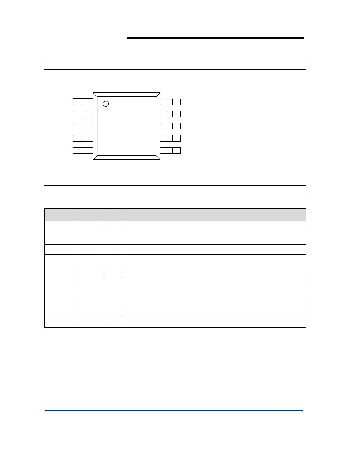
Pin Assignment
AP6015
High Efficiency Step-Down Low Power DC-DC Converter
( Top View )
PVCC
VCC
GND
FB/Vout
1
2
3
4
PG
56
MSOP-10L
10
9
8
7
PGND
LX
EN
NC
CC
Pin Descriptions
Pin Name Pin NO. I/O Description
PVCC 1 I
VCC 2
GND 3 Ground
PG 4 O
FB 5 I Feedback pin for the fixed output voltage option.
Supply voltage input
Supply bypass pin. A 1μF coupling c apacitor s hould be conn ected as cl ose
as possible t o t hi s pi n.
Power good comparator output. A pull-up resistor should be connected
between PG and V
.
O
CC 6 I Compensation pin
NC 7 NC
EN 8 I Enable.Pin, H: Enable. L:shutdown
LX 9 I/O Connect the inductor to this pin.
PGND 10 Power ground
AP6015 Rev. 3 2 of 18 FEBRUARY 2009
No connect
www.diodes.com © Diodes Incorporated
Page 3
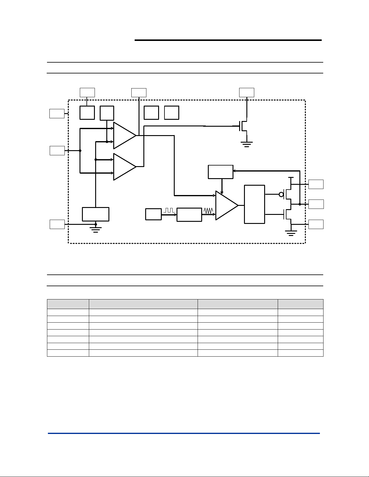
)
Block Diagram
VCC
AP6015
High Efficiency Step-Down Low Power DC-DC Converter
CC
CC
PG
PG
EN
CE
UVLO
SSSS
TS Bias
Open drain
-
ER-AMP
+
FB
FB
Vref=0.8V
-
PG_COM
+
BANDGAP
Osc
Vramp
GND
Notes: 3. The adjustable output voltage version does not use the internal feedback resistor divider.
The FB pin is directly connected to the error amplifier.
Current
Protection
+
PWM-COM-
-
Buffer
PVCC
PVCC
LX
PGND
PGND
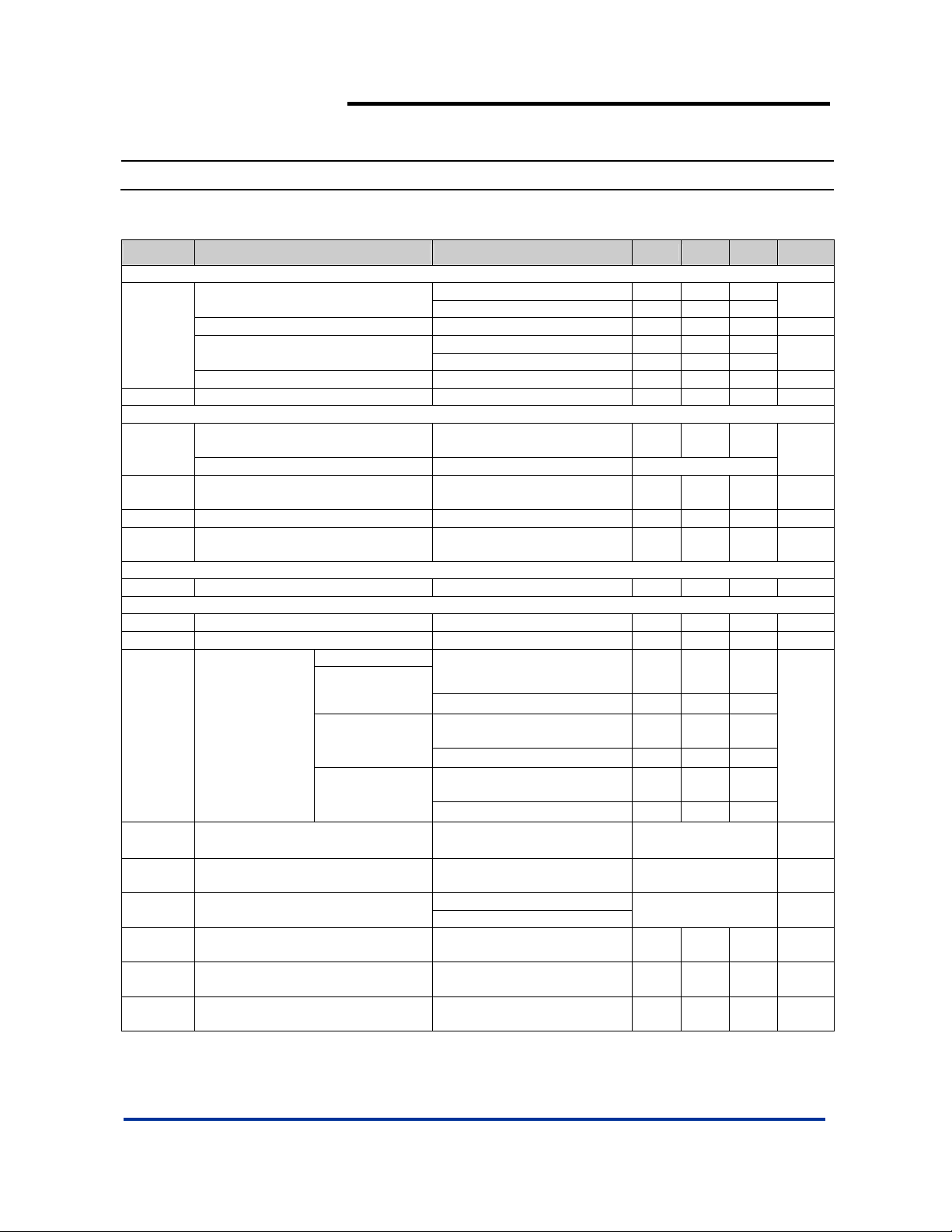
Absolute Maximum Ratings
Symbol Parameter Rating Unit
ESD HBM Human Body Model ESD Protection 2.5 KV
ESD MM Machine Model ESD Protection 300 V
PVCC, VCC Supply Voltage -0.3 to +5.5 V
Voltages on pins EN, CC, PG, FB, LX -0.3 to VIN +0.3 V
T
Maximum Junction Temperature Range +150
J(MAX
TST Storage temperature range -65 to +150
TOP Operating Junction Temperature Range -40 to +125
Stresses beyond those listed under “absolute maximum ratings” may cause permanent damage to the device. These are stress rati ngs only and functional
operation of the device at these or any other conditions beyond those indicated under “recommended operating conditions” is not impli ed. E xposure to
absolute-maximum-rated conditions for extended periods ma affect device reliability.
o
C
o
C
o
C
AP6015 Rev. 3 3 of 18 FEBRUARY 2009
www.diodes.com © Diodes Incorporated
Page 4
AP6015
High Efficiency Step-Down Low Power DC-DC Converter
Recommended Operating Conditions (T
:-40~85°C)
A
Symbol Parameter Rating Unit
TA Operating Ambient Temperature Range -40 to +85
o
C
VIN Supply Voltage 2.0 to 5.5 V
VO Output voltage range for adjustable output voltage version 0.8 to VI V
L Inductor (see Note 4) 3.3 μH
Ci Input capacitor (see Note 4) 10 μF
Co Output capacitor (see Note 4) VO ≥ 1.8V 10 μF
Notes: 4. Refer to application section for further information.
Electrical Characteristics (T
=25°C)
A
Over recommended operating free-air temperature range, VI=3.6V, VO=2.5V, IO=300mA, EN=VIN. (unless otherwise noted)
Symbol Parameter Conditions Min Typ. Max Unit
Supply current
I
= 0mA to 800mA 2.5 - 5.5
O
-20 to 85
o
C
IO= 0mA to 500mA 2 - 5.5
VIN Input Voltage range
-40 to 85 oC
I
= 0mA to 600mA 2.5 5.5
O
V
IO= 0mA to 400mA 2 - Iccq Operating quiescent current IO= 0mA - 150 - μA
I
Standby current EN= GND - 0.1 1 μA
STBY
Enable
≤ 3V 1.5 - -
V
VIH
EN high-level input voltage
IN
VIN> 3V 2.5 - -
VIL EN low-level input voltage - - 0.7 V
IL EN input leakage current EN= GND or VIN - 0.01 0.1 μA
V
Under-voltage-lockout-threshold 1.2 1.6 1.95 V
(UVLO)
V
AP6015 Rev. 3 4 of 18 FEBRUARY 2009
www.diodes.com © Diodes Incorporated
Page 5
(
)
(
)
(FB)
T
AP6015
High Efficiency Step-Down Low Power DC-DC Converter
Electrical Characteristics (Continued)
Over recommended operating free-air temperature range, VI=3.6V, VO=2.5V, IO=300 mA, EN=VIN. (unless otherwise noted)
Symbol Parameter Conditions Min Typ. Max Unit
Power switch and current limit
=3.6V; I=200mA 200 280 410
V
I=VGS
VI=VGS=2V; I=200mA - 480 V
=3.6V; IO=200mA 200 280 410
I=VGS
VI=VGS=2V; IO=200mA - 500 -
R
DS(on)
P-channel MOSFET on-resistance
P-channel leakage current VDS=5.5V - - 1 μA
N-channel MOSFET on-resistance
N-channel leakage current VDS=5.5V - - 1 μA
I
P-channel current limit 2.5V≤VI≤5.5V 1200 - 1600 mA
LIM
Power good output (see Note 5)
V
Power good threshold Feedback voltage falling
(PG)
88%
92%
V
O
VO
94%
VO
Power good hysteresis 2.5% VO
VOL PG output low voltage
I
PG output leakage current V
LKG
Minimum supply voltage for valid
power good signal
(FB)
I
=10μA
sink
=VO nominal 0.01 1 μA
1.2 - - V
- - 0.3 V
=0.8×VO nominal;
V
Oscillator
FS Oscillator frequency 800 1000 1200 KHz
Output
VO Adjustable output voltage range 0.8 5.5 V
V
Reference voltage 0.784 0.8 0.816 V
REF
AP6015-Adj
AP6015-1.8V
Fixed output
VO
voltage
(see Note 6)
AP6015-2.5V
AP6015-3.3V
Line regulation
Load regulation
η Efficiency
Start-up time
θ
θ
Notes: 5. Power good is not valid for the first 100μs after EN goes high. Please refer to the application section for more information.
double sided FR-4 PCB
Thermal Resistance
JA
Junction-to-Ambient
hermal Resistance
JC
Junction-to-Case
6. The output voltage accuracy includes line and load regulation over the full temperature range.
7. Test condition for MSOP-10L: Device mounted on 2oz copper, minimum recommended pad layout on top & bottom layer with thermal vias,
=2.5V to 5.5V;
V
I
0mA ≤ I
≤ 800mA
O
10mA ≤ IO ≤ 800mA
=2.7V to 5.5V;
V
I
0mA ≤ I
≤ 800mA
O
10mA ≤ IO ≤ 800mA
=3.6V to 5.5V;
V
I
0mA ≤ I
≤ 800mA
O
10mA ≤ IO ≤ 800mA
= VO +0.5 V ( min.2V )
V
I
to 6.0V; I
=10mA
O
VI=5.0V;
I
=10mA to 800mA
O
=5V; VO=3.3V; IO=300mA
V
I
VI=3.6V; VO=2.5V; IO=200mA
IO=0mA, time from
active EN to V
O
-3%
-3%
-3%
-3%
-3%
-3%
- 4%
- 3%
- 4%
- 3%
- 4%
- 3%
0.3 %/V
0.8 %
94 %
0.4 1 4 ms
MSOP-10L (Note 7) 161
MSOP-10L (Note 7) 39
mΩ
mΩ
o
C/W
o
C/W
V
V
AP6015 Rev. 3 5 of 18 FEBRUARY 2009
www.diodes.com © Diodes Incorporated
Page 6
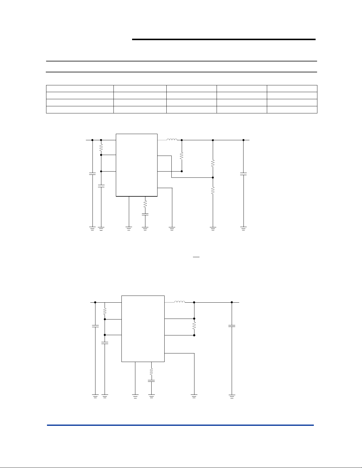
High Efficiency Step-Down Low Power DC-DC Converter
Typical Application Circuit
For best transient response we suggest that R
V
< 3.0V, V
IN
V
≥ 3.0V, V
IN
V
≥ 3.0V, V
IN
OUT
OUT
OUT
(1) ADJ Output
< 2.5V 200KΩ 33PF
< 2.5V
≥ 2.5V
R
C
CC
68KΩ 100PF
82KΩ 100PF
, C
and L1 values as below.
CC
CC
L1-WURTH C1, C2 (MLCC)
CC
AP6015
1.8µH 10µF
1.8µH 10µF
3.3µH 10µF
VI3.0 V to 5.5 V
C1
10µF
(2) FIXED Output
Typical Application
5 V
V
I
C1
10uF
L1
9
5
4
10
CC
R3
680K
Power Good
R1
C2
10µF
R2
because of stability reasons.
R
1
VV
REFO
)1(
+×=
R
2
100 Ohm
C3
1µF
1
2
8
PVCC
VCC
EN
GND
LX
FB
AP6015
PG
PGND
CC
63
Rcc
C
100pF
R2: Suggest to be 39K~100K
Typical Application Circuit for Adjustable Output Voltage Option
L1
LX
FB
PG
9
5
R3
4
680K
Power Good
1.8/ 2.5/ 3.3V/ 800mA
V
O
C2
10uF
100 Ohm
1
2
8
PVCC
VCC
AP6015
EN
2.5 V/800 mA
V
O
C3
1uF
GND CC
63
PGND
Rcc
C
100pF
10
CC
Standard 5 V to 1.8/ 2.5/ 3.3V/ 800mA Conversion; High Efficiency
AP6015 Rev. 3 6 of 18 FEBRUARY 2009
www.diodes.com © Diodes Incorporated
Page 7

High Efficiency Step-Down Low Power DC-DC Converter
Typical Operating Characteristics
AP6015
Input Voltage vs. Supply Current
250
200
150
100
Supply Current (uA)
50
0
22.533.644.555.5
Input Voltage (V)
Vout=0.8V
Vout=1.8V
Figure 1
Stand-by Current vs. Input Voltage
0.1
0.08
Supply Current vs. Temperature
250
200
150
100
Supply Current (uA)
50
0
(Vcc=3.6V Vout=2.5V)
-40 -25 0 25 50 85
Temperature (℃)
Figure 2
Stand-by C u rrent vs. Temperature
(Vcc=3.6V)
1.2
1
0.06
0.04
Stand-by Current (uA)
0.02
0
22.533.644.555.5
Input Voltage (V)
Figure 3
0.8
0.6
0.4
Stand-by Current (uA)
0.2
0
-40-250 255085
Temperature (℃)
Figure 4
AP6015 Rev. 3 7 of 18 FEBRUARY 2009
www.diodes.com © Diodes Incorporated
Page 8

)
High Efficiency Step-Down Low Power DC-DC Converter
Typical Operating Characteristics (Continued)
AP6015
Line Regulation
(Vout=2.5V Iout=10mA)
2.55
2.54
2.53
2.52
2.51
2.5
2.49
2.48
Output Voltage (V)
2.47
2.46
2.45
3.0V 3.6 4 4.5 5 5.5
Input Voltage (V)
Figure 5
Frequency vs. Temperature
(Vcc=3.6V Vout=2.5V)
1050
1000
Load Regulation
2.55
2.54
2.53
2.52
2.51
2.5
2.49
2.48
Output Voltage (V)
2.47
2.46
2.45
10 100 200 400 600 800
(Vcc=5.0V Vout=2.5V)
Ou tpu t Current (mA)
Figure 6
UVLO vs. Temperature
1.8
1.72
950
900
850
Frequency (KHz
800
750
-40 -25 0 25 50 85
Temperat ure (℃)
Figure 7
1.64
1.56
UVLO (V)
1.48
1.4
-40 -25 0 25 50 85
Temperature (
)
℃
Figure 8
AP6015 Rev. 3 8 of 18 FEBRUARY 2009
www.diodes.com © Diodes Incorporated
Page 9

)
)
High Efficiency Step-Down Low Power DC-DC Converter
Typical Operating Characteristics (Continued)
AP6015
Efficiency vs. Load Current
(Vcc=3.6V Vout=1.8V)
100
90
80
70
60
50
40
Efficiency (%
30
20
10
0
0 100 200 300 400 500 600 700 800
Load Current (mA)
Figure 9
Efficiency vs. Load Current
(Vcc=5.0V Vout=2.5V)
100
90
80
70
60
50
40
Efficiency (%)
30
20
10
0
0 100 200 300 400 500 600 700 800
Load Current (mA)
Figure 11
Efficiency vs. Load Current
(Vcc=3.6V Vout=2.5V)
100
90
80
70
60
50
40
Efficiency (%)
30
20
10
0
0 100 200 300 400 500 600 700 800
Load Current (mA)
Figure 10
Efficiency vs. Load Current
(Vcc=5.0V Vout=3.3V)
100
90
80
70
60
50
40
Efficiency (%
30
20
10
0
0 100 200 300 400 500 600 700 800
Load Current (mA)
Figure 12
AP6015 Rev. 3 9 of 18 FEBRUARY 2009
www.diodes.com © Diodes Incorporated
Page 10

High Efficiency Step-Down Low Power DC-DC Converter
Typical Operating Characteristics (Continued)
AP6015
Dropout Voltage vs. Load Current
(Vout=2.5V)
400
350
300
250
200
150
100
Dropout Voltage (mV)
50
0
0 100 200 300 400 500 600 700 800
Load Current (mA)
Figure 13 Figure 14
Output Ripple Output Ripple
Dropout Voltage vs. Load Current
(Vout=3.3V)
400
350
300
250
200
150
100
Dropout Voltage (mV)
50
0
0 100 200 300 400 500 600 700 800
Load Current (mA)
Figure 15
Figure 16
AP6015 Rev. 3 10 of 18 FEBRUARY 2009
www.diodes.com © Diodes Incorporated
Page 11

High Efficiency Step-Down Low Power DC-DC Converter
Typical Operating Characteristics (Continued)
Load Transient Response Load Transient Response
Figure 17 Figure 18
Load Transient Response Load Transient Response
AP6015
Figure 19
AP6015 Rev. 3 11 of 18 FEBRUARY 2009
www.diodes.com © Diodes Incorporated
Figure 20
Page 12

AP6015
High Efficiency Step-Down Low Power DC-DC Converter
Application Information
Enable (EN)
When EN is on logic low, the AP6015 goes into shutdown mode. In shutdown, all other functions are turned
off. The supply current is reduced to 1uA (Typ.).
Soft Start
As the enable pin goes high, the soft-start function generates an internal voltage ramp. This causes the
start-up current to slowly raise preventing output voltage overshoot and high inrush currents. The soft-start
duration is typical 1mSec.
AP6015 START-UP TIME
Under Voltage Lock Out (UVLO)
The UVLO prevents the converter from t urning on when the voltage on V
0V
0V
AP6015 Rev. 3 12 of 18 FEBRUARY 2009
www.diodes.com © Diodes Incorporated
is less than typically 1.6V.
CC
3.6V
Vcc
1.6V
UVLO
2.5V
Vout
Page 13

)
High Efficiency Step-Down Low Power DC-DC Converter
Application Information (Continued)
Power Good (PG)
AP6015
The PG comparator has an open drain output capable of sinking typically 10mA. The PG is only active when
the AP6015 is enable (EN=high). When the AP6015 is disable (EN=low), the PG pin is high impedance.
If the PG pin is connected to the output of the AP6015 with a pull-up resistor, no initial spike occurs and
precautions have to be taken during start-up.
The PG pin becomes active high when the output voltage exceeds typically 92% of its nominal value. Leave
the PG pin unconnected when not used.
PG Sink Current vs. ExteranI Voltage
25
20
15
10
PG Sink Current (mA
5
0
2 2.5 3 3.6 4 4.5 5 5.5
Extern al Vol t age (V)
AP6015 Rev. 3 13 of 18 FEBRUARY 2009
www.diodes.com © Diodes Incorporated
Page 14

AP6015
High Efficiency Step-Down Low Power DC-DC Converter
Application Information (Continued)
Inductor Selection
In order to avoid saturation of the inductor, the inductor should be rated at least for the maximum output
current plus the inductor ripple current which is calculated as:
V
O
−
VI
×=Δ
OL
Where:
f= Switching frequency (1MHz typical)
L = Inductor value
△I
= Peak-to-peak inductor ripple current
L
I
(max) = Maximum inductor current
L
Vcc=3.6V Vout=2.5V f=1MHz L=3.3uH
Î△I
≒230mA
L
)(1
V
CC
fL
×
II
MAXOMAXL
I
Δ
L
+=
)()(
2
Vcc=3.6V Vout=2.5V f=1MHz L=1.8uH
Î△IL≒360mA
AP6015 Rev. 3 14 of 18 FEBRUARY 2009
www.diodes.com © Diodes Incorporated
Page 15

AP6015
High Efficiency Step-Down Low Power DC-DC Converter
Application Information (Continued)
Input Capacitor Selection
Though there is no special requirement for the ESR (Equivalent Series Resistance) of the input capacitor, due
attention should be paid to the tolerance and temperature coefficient of the capacitor used. A 10uF or larger
capacitance is required between the PVCC and the GND pins. The input capacitor should be placed as
close as possible to the PVCC pin in order to achieve good overall system performance.
Output Capacitor Selection
Ripple at the voltage output pin is caused by the charge-and-discharge of the output capacitor. For the best
performance, a low ESR output capacitor should be used. The equation below demonstrates how the size of
the ripple can be calculated.
V
O
−
VV
×=Δ
OO
Where:
△Vo= Output voltage ripple
)(1
V
CC
×
×
1
(
8
fCfL
××
O
IESR
×Δ=+
L
1
()
8
+
fC
××
O
ESR
)
L = Inductor value
f = Switching frequency (1MHz typical)
△I
= Peak-to-peak inductor ripple current
L
AP6015 Rev. 3 15 of 18 FEBRUARY 2009
www.diodes.com © Diodes Incorporated
Page 16

AP6015
High Efficiency Step-Down Low Power DC-DC Converter
Application Information (Continued)
Layout Considerations
A good board layout practice can significantly improve the stability of the application circuit and reduce the
system noise. The feedback path must be as short as possible. The input capacitor and bypass capacitor
must be placed close to the PVCC and the VCC pins for optimal performance. It is recommended that the
ground planes for System Ground / Power Ground / Analog Ground are isolated from each others, while they
should all be joined together at a common point. An example drawing of a circuit with good ground noise
performance is shown below.
L1
V
C1
10µF
1
I
C3
1µF
100 Ohm
10
2
PVCC
VCC
AP6015
EN
PGND
GND CC
63
LX
FB
PG
Rcc
C
CC
100 pF
9
5
48
R3
680K
R1
Power Good
R2
V
C2
10 uF
O
The external induc tor m ust be pl aced as clos e as pos sible t o the s witc hing no de, i. e. th e LX pin. The co pper
traces on the pcb, where high peak switching current may flow through, should be kept ‘wide’ and ‘short’.
This results in low inductance and capacitance in the current path, hence ground shift problem is avoided and
system stability stay within bound.
AP6015 Rev. 3 16 of 18 FEBRUARY 2009
www.diodes.com © Diodes Incorporated
Page 17

High Efficiency Step-Down Low Power DC-DC Converter
Marking Information
( Top View )
10
9876
Logo
Part Number
6015XX
XX : 18 for 1.8V
25 for 2.5V
33 for 3.3V
Blank for ADJ
245
1
MSOP-10L
Package Information (All Dimensions in mm)
(1) Package type: MSOP-10L
W X
Y
3
AP6015
A~Z : Green
Y : Year : 0~9
W
: Week : A~Z : 1~26 week;
a~z : 27~52 week; z represents
52 and 53 week
0.10
0.1/0.2
C
1
0.17/0.27
2.95/3.05
0.5Typ.
1
4.8/5.0
2.95/3.05
10x-1.4
Land Pattern Recommendation
0.75/0.95
1.10Max.
C
0.05/0.15
Seting plane
0.4/0.7
10x-0.30
8x-0.50
4.4
1
(Unit:mm)
0.25
Gauge plane
8°
/
°
0
"A"
DETAIL "A"
AP6015 Rev. 3 17 of 18 FEBRUARY 2009
www.diodes.com © Diodes Incorporated
Page 18

AP6015
High Efficiency Step-Down Low Power DC-DC Converter
IMPORTANT NOTICE
Diodes Incorporated and its subsidiaries reserve the right to make modifications, enhancements, improvements, corrections or other changes without further
notice to any product herein. Diodes Incorporated does not assume any liability arising out of the application or use of any product described herein; neither
does it convey any license under its patent rights, nor the rights of others. The user of products in such applications shall assume all risks of such use and will
agree to hold Diodes Incorporated and all the companies whose products are represented on our website, harmless against all damages.
LIFE SUPPORT
Diodes Incorporated products are not authorized for use as critical components in life support devices or systems without the expressed written approval of the
President of Diodes Incorporated.
AP6015 Rev. 3 18 of 18 FEBRUARY 2009
www.diodes.com © Diodes Incorporated
 Loading...