

Page 1
AP5002
PWM CONTROL 2A STEP-DOWN CONVERTER
Features
• Input voltage: 3.6V to 20V
• Output voltage: 0.8V to V
• Duty ratio: up to 100% PWM control
• Oscillation frequency: 500KHz typical
• Soft-start Current Limit, Enable function
• Thermal Shutdown function
• Built-in internal SW P-channel MOS
• Low ESR output capacitor (MLCC, multi-layer ceramic
capacitor) support
• Efficiency 90%
• SOP-8L: Available in “Green” Molding Compound
(No Br, Sb)
• Lead Free Finish / RoHS Compliant (Note 1)
CC
Applications
• PC Motherboard
• LCD Monitor
• Graphic Card
• DVD-Video Player
• Telecom Equipment
• ADSL Modem
• Printer and other Peripheral Equipment
• Microprocessor core supply
• Networking power supply
General Description
AP5002 consists of step-down switching regulator with
PWM control. These devices include a reference voltage source,
oscillation circuit, error amplifier, internal PMOS.
AP5002 provides low-ripple power, high efficiency, and excellent
transient characteristics. The PWM control circuit is able to vary
the duty ratio linearly up to 100%. This converter also contains
an error amplifier circuit as well as a soft-start circuit that prevents
overshoot at startup. An enable function, an over current protect
function and a short circuit protect function are built inside, and
when OCP or SCP happens, the operation frequency will be
reduced from 500KHz to 50KHz. Also, an internal compensation
block is built in to minimum external component count.
With the addition of an internal P-channel Power MOS, a coil,
capacitors, and a diode connected externally, these ICs can
function as step-down switching regulators. They serve as ideal
power supply units for portable devices when coupled with the
SOP–8L mini-package, providing such outstanding features as
low current consumption. Since this converter can accommodate
an input voltage up to 22V, it is also suitable for the operation via
an AC adapter.
Ordering Information
AP5002 S G - 13
Package
S : SOP-8L
Device
AP5002SG-13 S SOP-8L 2500/Tape & Reel -13
Notes: 1. EU Directive 2002/95/EC (RoHS). All applicable RoHS exemptions applied. Please visit our website at
http://www.diodes.com/products/lead_free.html
2. Pad layout as shown on Diodes Inc. suggested pad layout document AP02001, which can be found on our website at
http://www.diodes.com/datasheets/ap02001.pdf
AP5002 Rev. 8 1 of 10 FEBRUARY 2009
Package
Code
Packaging
(Note 2)
.
.
www.diodes.com © Diodes Incorporated
Green
G : Green
Packing
13 : Tape & Reel
13” Tape and Reel
Quantity Part Number Suffix
Page 2
(
AP5002
PWM CONTROL 2A STEP-DOWN CONVERTER
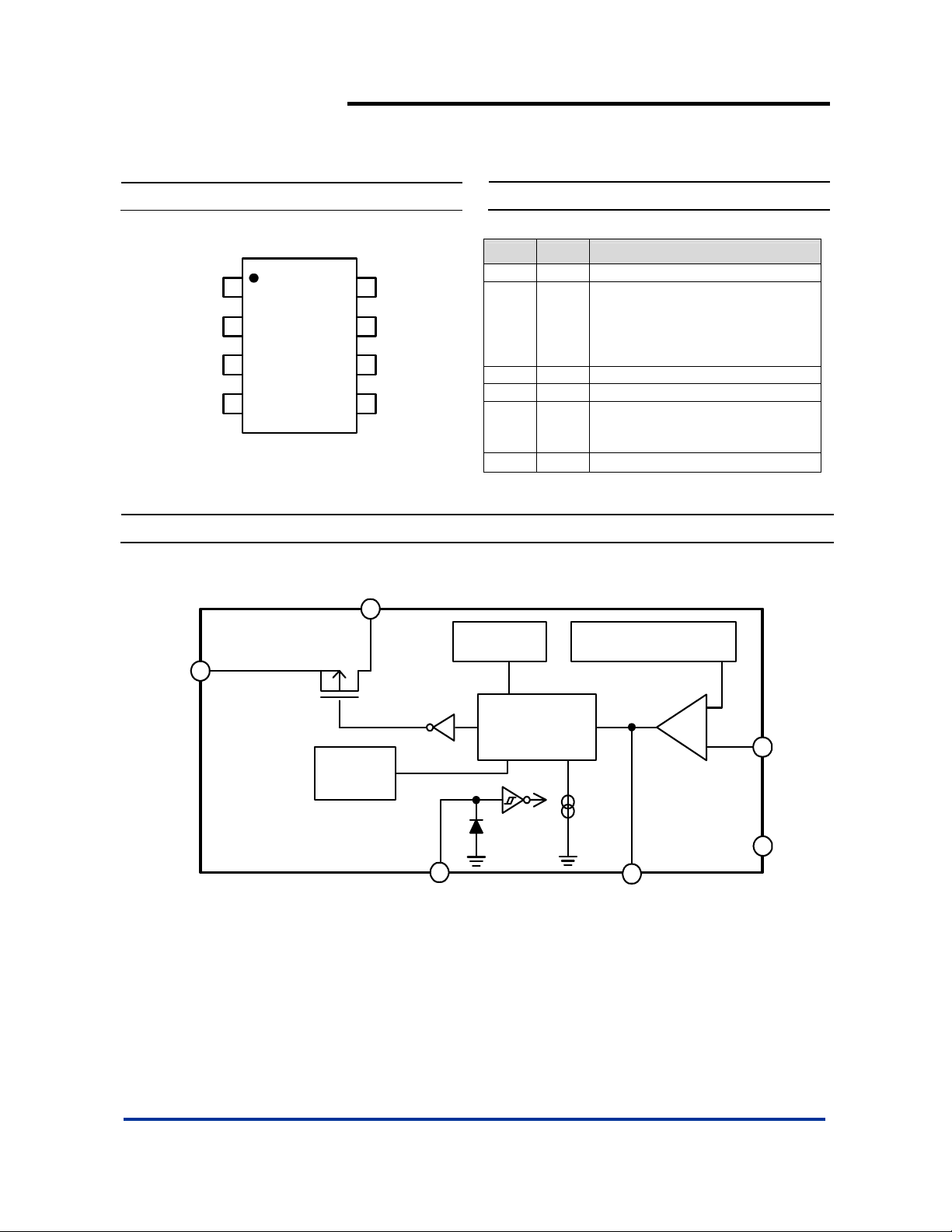
Pin Assignments
( Top View )
1
FB
2
EN
Comp
CC
V
AP5002
3
4
SOP-8L
Block Diagram
Vcc
8
7
6
5
Vss
Vss
Output
Output
Output
Pin Descriptions
Name Pin Description
FB 1 Feedback pin
Power-off pin
H: Normal operation
EN 2
Comp 3 Compensation pin
VCC 4 IC power supply pin
Output
VSS
Oscillation
Circuit
(Step-down operation)
L: Step-down operation stopped
All circuits deactivated)
Switch Pin. Connect external
5、6
inductor/diode here. Minimize trace
area at this pin to reduce EMI.
7、8
GND Pin
Reference Voltage Source
+
FB
-
Vss
Thermal
Shutdown
EN
PWM-Switched
Control Circuit
V
EN
100uA
Comp
AP5002 Rev. 8 2 of 10 FEBRUARY 2009
www.diodes.com © Diodes Incorporated
Page 3
AP5002
PWM CONTROL 2A STEP-DOWN CONVERTER
Absolute Maximum Ratings
Symbol Parameter Rating Unit
ESD HBM Human Body Model ES D Protection
5
ESD MM Machine Model ESD Protection 200 V
VCC VCC Pin Voltage VSS - 0.3 to VSS + 22 V
VFB Feedback Pin Voltage VSS - 0.3 to VCC V
VEN EN Pin Voltage VSS - 0.3 to VIN V
V
Switch Pin Voltage VSS- 0.3 to VIN V
OUTPUT
PD Power Dissipation 1000 mW
TJ Operating Junction Temperature Range -20 to +125
T
Storage Temperature Range -65 to +150
ST
Caution: The absolute maximum ratings are rated values exceeding which the product could suffer physical damage. These values must therefore not be
exceeded under any conditions.
Recommended Operating Conditions
Symbol Parameter Min Max Unit
VIN Input Voltage 3.6 20 V
I
Output Current 0 2 A
OUT
TA Operating Ambient Temperature -20 85 oC
AP5002 Rev. 8 3 of 10 FEBRUARY 2009
www.diodes.com © Diodes Incorporated
KV
o
C
o
C
Page 4

T
AP5002
PWM CONTROL 2A STEP-DOWN CONVERTER
Electrical Characteristics (VIN = 12V, T
= 25°C, unless otherwise specified)
A
Symbol Parameter Conditions Min Typ. Max Unit
VFB Feedback Voltage I
IFB Feedback Bias Current I
I
Quiescent Current VFB= 1.2 force drive off - 3 5 mA
CCQ
= 0.1A 0.784 0.8 0.816 V
OUT
= 0.1A - 0.1 0. 5 µA
OUT
ISW Switch Current -- 3.5 - - A
ISD Shutdown Supply Current VEN = 0V - 10 - µA
∆V
OUT
/V
∆V
/V
Line Regulation V
OUT
OUT
Load Regulation I
OUT
f
Oscillation Frequency Measure waveform at SW pin 400 500 600 KHz
OSC
VSH
EN Pin Input Voltage
VSL Evaluate oscillation stop at SW pin - - 0.8
ISH
EN Pin Input Leakage
Current
ISL Ven = 0.8V -10 - 10 µA
= 4V~20V, I
IN
= 0.1 to 2A - 0.5 1 %
OUT
Evaluate oscillation at SW pin 2. 0 - -
= 0.2A - 1 2 %
OUT
V
Ven = 2V -10 - 10 µA
TSS Soft-Start Time -- - 3 - ms
= 5V, V
V
R
Internal MOSFET Rdson
DSON
Notes: 3. Test condition: Device mounted on 2oz copper, minimum recommended pad layout, FR-4 PCB.
Thermal shutdown 140
Minimum Duty Cycle
Thermal Resistance
θ
JA
Junction-to-Ambient
θ
hermal Resistance
JC
Junction-to-Case
IN
V
= 12V, V
IN
6.5 %
SOP-8L (Note 3) 124
SOP-8L (Note 3) 25
= 0V - 110 150
FB
= 0V - 70 100
FB
mΩ
o
o
C/W
o
C/W
C
AP5002 Rev. 8 4 of 10 FEBRUARY 2009
www.diodes.com © Diodes Incorporated
Page 5

Typical Application Circuit
AP5002
PWM CONTROL 2A STEP-DOWN CONVERTER
VIN+12V
Notes: 4. V
VIN+12V
U1
C2
22uF
C3
0.1uF
R5
100K
C6
0.1uF
ON/OFF
1
FB
2
EN
3
COMP
4 5
VCC Output
AP5002
R4
0.8~2K
VSS
VSS
Output
C7
0.1uF
8
7
6
Compensation Capacitor Selection(MLCC)
VIN VOUT R4 C7
12V 5/ 3.3/ 2.5/ 1.8/ 1.5V 0.8~2K 0.1µF
5V 3.3/ 2.5/ 1.8/ 1.5V 0.8~2K 27nF
C2
470uF
OUT
C3
0.1uF
= V
U1
FB
1
ON/OFF
R5
100K
C6
0.1uF
R1
)
FB
(1 +×
R2
2
3
4
R4
4.7~6.8K
EN
COMP
VCC
AP5002
VSS
VSS
Output
Output
C7
33nF
8
7
6
5
L1-(WURTH S05100104)
10uH
1 2
D1
Dii 723
B340A
L1-(WURTH S05100104)
10uH
1
D1
Dii 723
B340A
VOUT = 3.3V
C1
3.8K
1.2K
R1
R2
330pF
C8
0.1uF
C4
22uF
C1
330pF
330pF
VOUT = 3.3V
2
R1
3.8K
R2
1.2K
C1
330pF
C8
0.1uF
C4
470uF
AP5002 Rev. 8 5 of 10 FEBRUARY 2009
www.diodes.com © Diodes Incorporated
Page 6

PWM CONTROL 2A STEP-DOWN CONVERTER
Typical Performance Characteristics
AP5002 Vin vs. Frequency
570
560
550
540
530
Frequency(KHZ)
520
510
(Vout=3.3V; Iout=0.2A)
0 5 10 15 20 25
Vin(V)
AP5002
AP5002 Tem p eratur e vs. Frequen cy
575
560
545
530
515
Frequency(KHZ)
500
485
-20 0 20 40 60 80 100 120
(Vout=3.3V; Iout=0.2A)
Temperature(℃)
AP5002 V in vs. FB
0.808
0.806
0.804
VFB(V)
0.802
0.8
(Vout=3.3V; Iout=0.2A)
0 5 10 15 20 25
Vin(V)
AP5002 Effici en cy
100
90
Vout=5V
80
70
60
50
40
30
Efficiency(%)
20
10
0
0 0.5 1 1.5 2
Vout=3.3V
Iout(A )
AP5002 Temperature vs. FB
(Vout=3.3V; Iou t=0.2A)
0.82
0.81
0.8
VFB (V)
0.79
0.78
-2030 80130
Temperature(℃)
AP5002 Rev. 8 6 of 10 FEBRUARY 2009
www.diodes.com © Diodes Incorporated
Page 7

PWM CONTROL 2A STEP-DOWN CONVERTER
Typical Performance Characteristics (Continued)
AP5002 Load Regu lation
3.35
AP5002 Line Re gulation
3.35
AP5002
3.34
3.33
Vout(V)
3.32
3.31
3.3
00.511.52
AP5002 V i n vs. I
5
4
3
(mA)
CCQ
2
I
1
0
0 5 10 15 20
Iout( A)
(Vou t=3. 3V)
CCQ
Vin(V)
3.34
3.33
Vout(V)
3.32
3.31
3.3
0 5 10 15 20 25
AP5002 Temperature vs. I
Vin(V)
CCQ
(Vout=3.3V)
5
4.5
4
3.5
3
(mA)
2.5
CCQ
I
2
1.5
1
0.5
0
-20 0 20 40 60 80 100 120
Temperature(℃)
AP5002 Rev. 8 7 of 10 FEBRUARY 2009
www.diodes.com © Diodes Incorporated
Page 8

V
A
PWM CONTROL 2A STEP-DOWN CONVERTER
Typical Performance Characteristics (Continued)
AP5002
(Vin=12V; Vout=5V; Iout=0.2A)
out Ripple
(Vin=12V; Vout=5V; Iout=2A)
AP5002
P5002 Vout Ripple
Test Circuit
A
Enable function test Feedback function test
+
-
22u
1500p
A
Oscillation
+
-
6.8K
+
-
V
1.2K
COMP
EN
open
OUTPUT OUTPUT
COMP
EN
VCC
EN
VSS
OUTPUT
VSS
FB
COMP
open
FBVCC
6.8K
FBVCC
VSS
Operati on function test
AP5002 Rev. 8 8 of 10 FEBRUARY 2009
www.diodes.com © Diodes Incorporated
Page 9

R
Δ
=
AP5002
PWM CONTROL 2A STEP-DOWN CONVERTER
Functional Description
PWM Control
The AP5002 consists of DC/DC converters that employ a
pulse-width modulation (PWM) system.
In converters of the AP5002, the pulse width varies in a range up
to 100%, according to the load current. The ripple voltage
produced by the switch ing can ea sily be re moved t hrough a filter
because the switching frequency remains constant. Therefore,
these converters provide a low-ripple power over broad ranges of
input voltage and load current.
Current Limiting
R
DS(ON)
The current limit threshold is set by the internal circuit.
Setting the Output Voltage
Application cir cuit item shows the basic applic ation circuit with
adjustable output version. The external resistor sets the output
voltage according to the following equation:
V
(V)
OUT
5 6.4 1.2
3.3 3.8 1.2
2.5 2.6 1.2
1.8 3.3 2.6
1.5 3.3 3.7
1.2 3.3 6.5
1 3.3 13
Inductor Selection
For most designs, the operates with inductors of 10µH to
22µH. The inductor value can be derived from the following
equation:
()
=
L
Where is inductor Ripple Current. Large value inductors lower
ripple current and small value inductors result in high ripple
currents. Choose inductor ripple current approximately 15% of the
maximum load current 2A, ∆IL=0.3A. The DC current rating of the
inductor should be at least equal to the maximum load current
plus half the ripple current to prevent core saturation (2A+0.15A).
Input Capacitor Selection
EL CAP
This capacitor should be located close to the IC using short leads
and the voltage rating should be approximately 1.5 times the
maximum input volta ge. The RMS current rati ng requirement for
the input capacitor of a buck regulator is approximately 1⁄2 the
DC load current. A low ESR input capacitor sized for maximum
RMS current must be used. A 470µF low ESR capacitor for most
applications is sufficient.
MLCC CAP
A 22µF MLCC capacitor for most applications is sufficient.
Output Capacitor Selection
EL CAP
The output capacitor is required to filter the output voltage and
provides regulator loop stability. The important capacitor
parameters are the 100KHz Equivalent Series Resistance (ESR),
the RMS ripples current rating, voltage rating and capacitance
−
R1 (KΩ) R2 (KΩ)
TVV
ONOUTIN
×Δ×
fI2
oscL
AP5002 Rev. 8 9 of 10 FEBRUARY 2009
www.diodes.com © Diodes Incorporated
value. For the output capacitor, the ESR value is the most
important parameter . The output ripple can be calculated fro m
the following formula.
ES
IV
×
The bulk capacitor’s ESR will determine the output ripple voltage
and the initial voltage drop after a high slew-rate transient.
An aluminum electrolytic capacitor's ESR value is related to the
capacitance and its voltage rating. In most case, higher voltage
electrolytic capacitors have lower ESR values. Most of the time,
capacitors with much higher voltage ratings may be needed to
provide the low ESR values required for low output ripple v oltage .
MLCC CAP
A 22µF MLCC capacitor for most applications is sufficient.
PCB Layout Guide
If you need low T
SW pins(5& 6) and VSS pins(7& 8)on the SOP-8L package are
internally connecte d to die pad, Th e PCB layout s hould all ow for
maximum possible copper area at the SW pins.
1. Connect C3 to VCC and VSS pin as closely as possible to get
good power filter effect.
2. Connect R4 to VCC and OCSET pin as closely as possible.
3. Connect ground side of the C2 & D1 as closely as possible.
Typical PC Board Layout
Top Side Layout Guide
Use vias to conduct the heat into the backside of
PCB layer. The PCB heat sink copper area should be
solder-painted without masked. This approa ches a
“best case” pad heat sink.
Bottom Side Layout Guide
& TJ or large PD(Power Dissipation), The dual
C
LRIPPLE
Page 10

Marking Information
AP5002
PWM CONTROL 2A STEP-DOWN CONVERTER
( Top View )
8
5
Logo
Part Number
AP5002
YY
WW X
X
41
Package Information (All Dimensions in mm)
0.254
0.62/0.82
7°~9°
Gauge Plane
Seating Plane
7°~9°
1.27typ
4.85/4.95
0.3/0.5
3.85/3.95
5.90/6.10
0.10/0.20
Detail "A"
0.35max.
45°
0.15/0.25
1.30/1.50
1.75max.
G : Green
: Year : 08, 09,10~
YY
WW : Week : 01~52; 52
represents 52 and 53 week
: Internal Code
X
Detail "A"
0°/8°
8x-0.60
5.4
6x-1.27
8x-1.55
Land Pattern Recommendation
(Unit: mm)
IMPORTANT NOTICE
Diodes Incorporated and its subsidiaries reserve the right to make modifications, enhancements, improvements, corrections or other changes without further
notice to any product herein. Diodes Incorporated does not assume any liability arising out of the application or use of any product described herein; neither
does it convey any license under its patent rights, nor the rights of others. The user of products in such applications shall assume all risks of such use and will
agree to hold Diodes Incorporated and all the companies whose products are represented on our website, harmless against all damages.
LIFE SUPPORT
Diodes Incorporated products are not authorized for use as critical components in life support devices or systems without the expressed written approval of the
President of Diodes Incorporated.
AP5002 Rev. 8 10 of 10 FEBRUARY 2009
www.diodes.com © Diodes Incorporated
 Loading...