

Page 1
AP4312
Document number: DS36797 Rev. 1 - 2
1 of 11
www.diodes.com
January 2014
© Diodes Incorporated
AP4312
A Product Line of
Diodes Incorporated
Description
The AP4312 is a highly integrated solution for a constant
voltage/constant current mode SMPS application.
The AP4312 contains one 1.21V voltage reference, one low voltage
reference used in current sensing circuit and two operational
amplifiers. The 1.21V voltage reference, combined with one
operational amplifier, makes of an ideal voltage controller for use in
adapters and battery chargers. The low voltage reference, combined
with another operational amplifier, makes of an ideal current limiter for
output low side current sensing.
The AP4312 is fully compatible with AP4306 in functionality and
electrical characteristics except its lower reference voltage for current
control loop, thus higher power efficiency in SMPS applications such
as low power charger can be realized with AP4312 compared to
AP4306.
The AP4312 is available in SOT26 package.
Features
Constant Voltage and Constant Current Control
Precision Internal Voltage Reference
Low External Component Count
Easy Compensation
Low Supply Current: 180A
Current Control Loop Reference: 70mV
Operating Supply Voltage: 1.7V to 18V
Totally Lead-free & Fully RoHS Compliant (Note 1 & 2)
Halogen and Antimony Free. “Green” Device (Note 3)
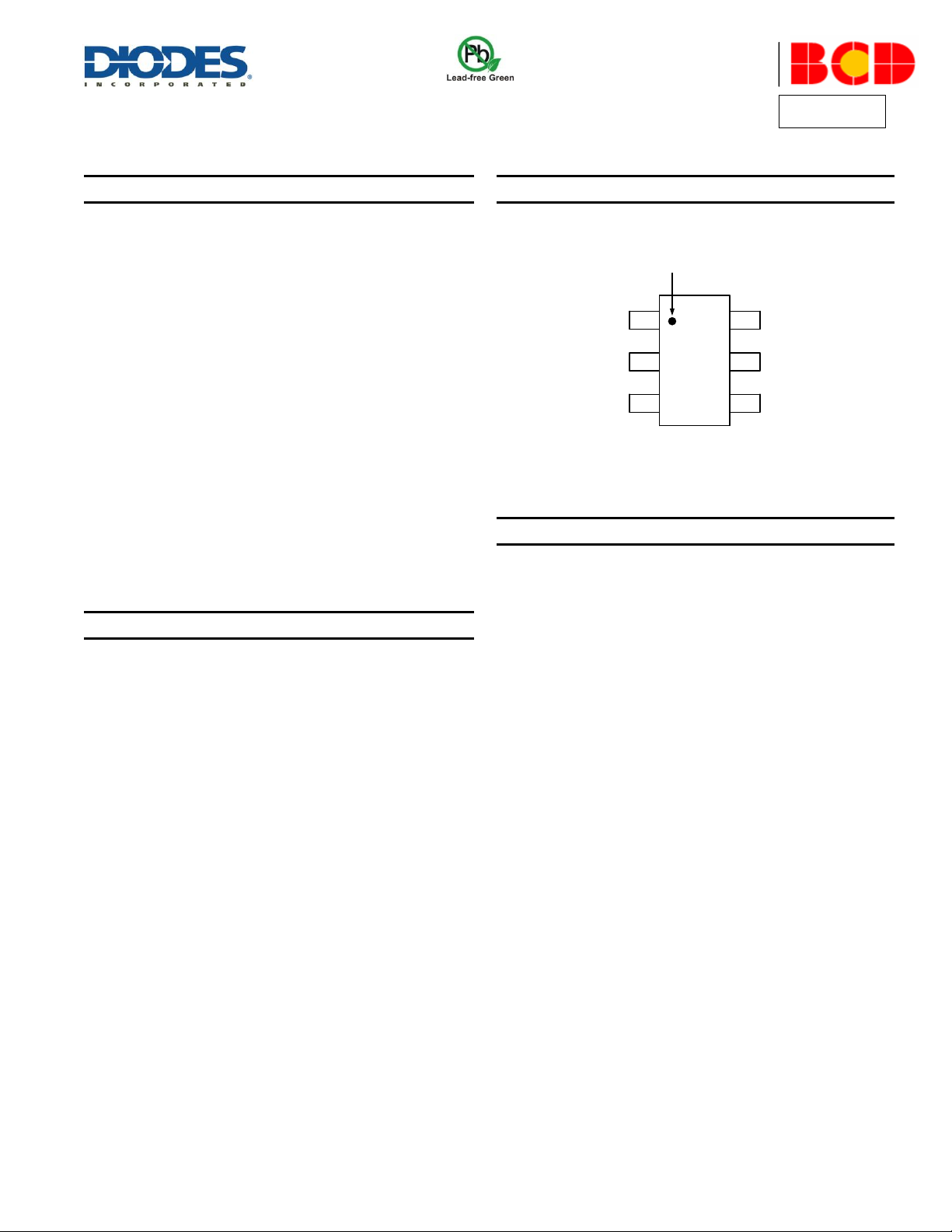
Pin Assignments
(Top View)
1
2
3 4
5
Pin 1 Mark
6
V
SENSE
GND
V
CTRL
I
CTRL
V
OUT
V
CC
SOT26 (K6 Package)
Applications
Adapters
Battery Chargers
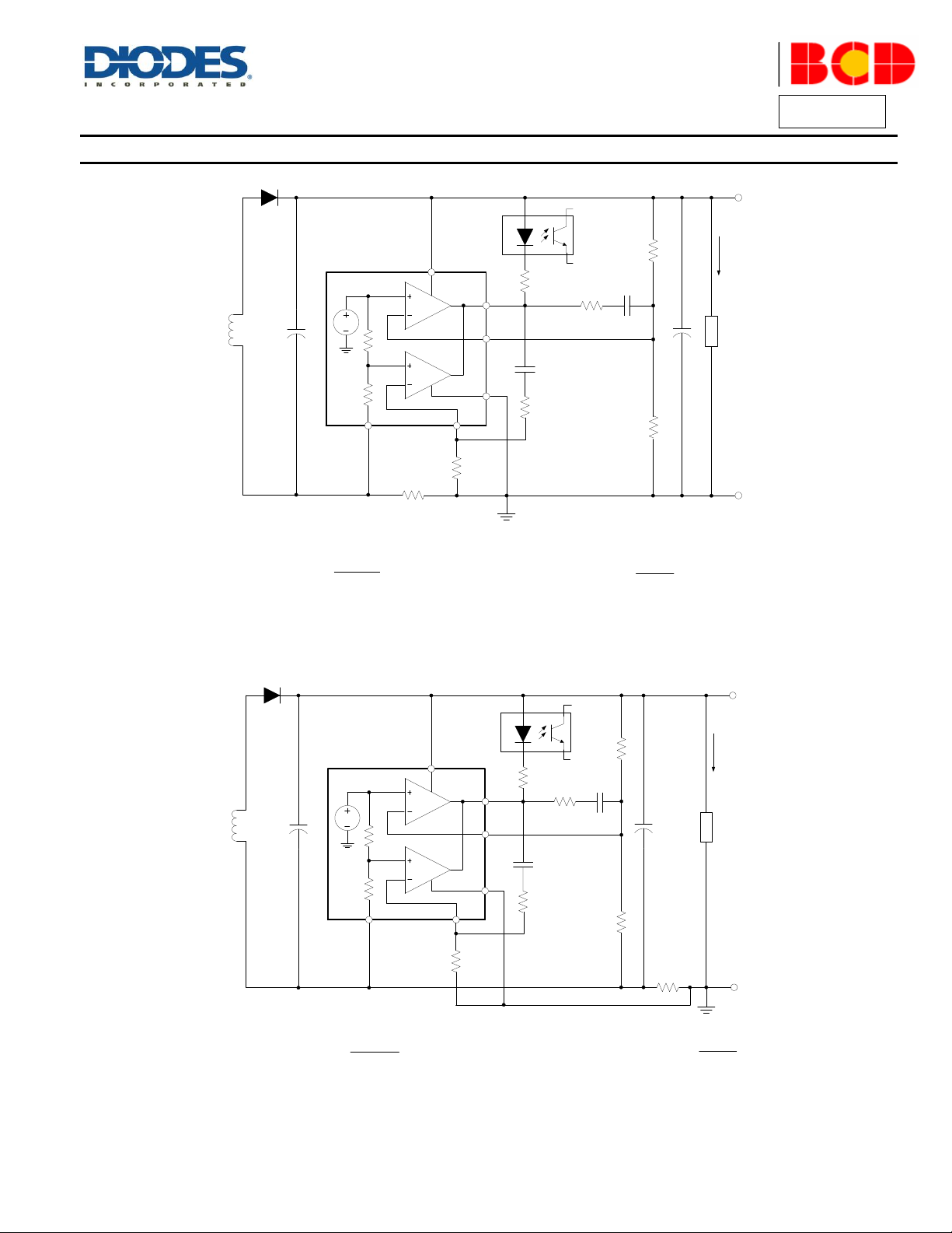
CONSTANT VOLTAGE AND CONSTANT CURRENT CONTROLLER
Notes: 1. No purposely added lead. Fully EU Directive 2002/95/EC (RoHS) & 2011/65/EU (RoHS 2) compliant.
2. See http://www.diodes.com/quality/lead_free.html for more information about Diodes Incorporated’s definitions of Halogen- and Antimony-free, "Green"
and Lead-free.
3. Halogen- and Antimony-free "Green” products are defined as those which contain <900ppm bromine, <900ppm chlorine (<1500ppm total Br + Cl) and
<1000ppm antimony compounds.
Page 2
AP4312
Document number: DS36797 Rev. 1 - 2
2 of 11
www.diodes.com
January 2014
© Diodes Incorporated
AP4312
A Product Line of
Diodes Incorporated
1.210V
V
CC
V
OUT
GND
V
SENSE
I
CTRL
R
SS
R4
To
primary
R2
R1
V
OUT
+
V
OUT
-
Load
C1
R3
C3
R5
R6
500
V
CTRL
AP4312
+
+
I
L
)(
1
21
)]([
SSLSSLREF
UT
O
RI
R
RR
RIVV
SS
SENSE
R
V
itCurrentLim
1.210V
V
CC
V
OUT
GND
V
SENSE
I
CTRL
R
SS
R4
To
primary
R2
R1
V
OUT
+
V
OUT
-
Load
C1
R3
C3
R5
R6
500
V
CTRL
AP4312
+
+
I
L
121R
RR
VV
REFOUT
SS
SENSE
R
V
itCurrentLim
Typical Applications Circuit
Typical Application 1
Typical Application 2
Page 3
AP4312
Document number: DS36797 Rev. 1 - 2
3 of 11
www.diodes.com
January 2014
© Diodes Incorporated
AP4312
A Product Line of
Diodes Incorporated
Pin Number
Pin Name
Function
1
V
CTRL
Input pin of the voltage control loop
2
GND
Ground 3 V
OUT
Output pin. Sinking current only
4
I
CTRL
Input pin of the current control loop
5
V
SENSE
Input pin of the current control loop
6
VCC
Power Supply
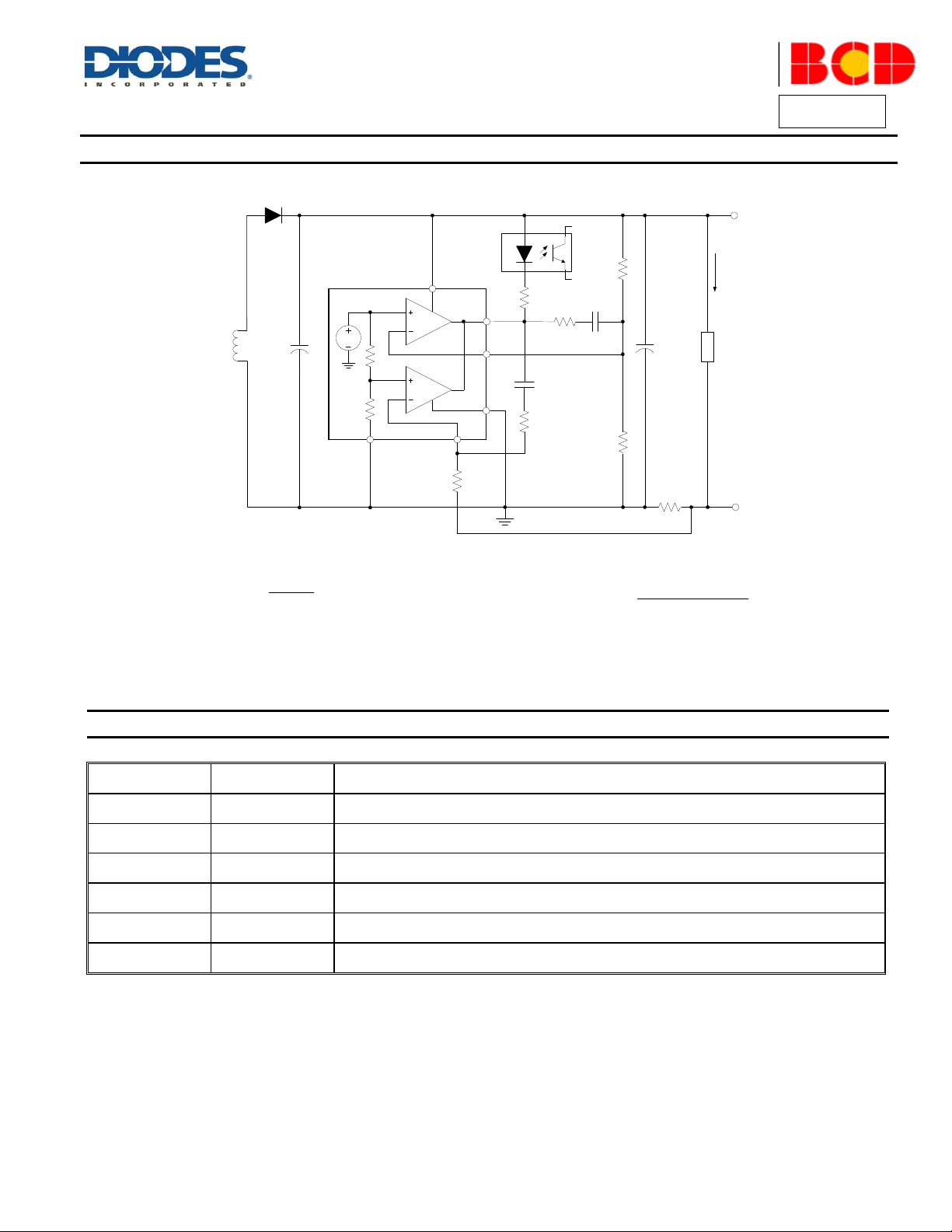
)(
1
21
SSLREFOUT
RI
R
RR
VV
SSREFSENSE
REFSENSE
RVV
VV
itCurrentLim
1.210V
V
CC
V
OUT
GND
V
SENSE
I
CTRL
R
SS
R4
To
primary
R2
R1
V
OUT
+
V
OUT
-
Load
C1
R3
C3
R5
R6
500
V
CTRL
AP4312
+
+
I
L
Typical Applications Circuit (Cont.)
Typical Application 3
Pin Descriptions
Page 4
AP4312
Document number: DS36797 Rev. 1 - 2
4 of 11
www.diodes.com
January 2014
© Diodes Incorporated
AP4312
A Product Line of
Diodes Incorporated
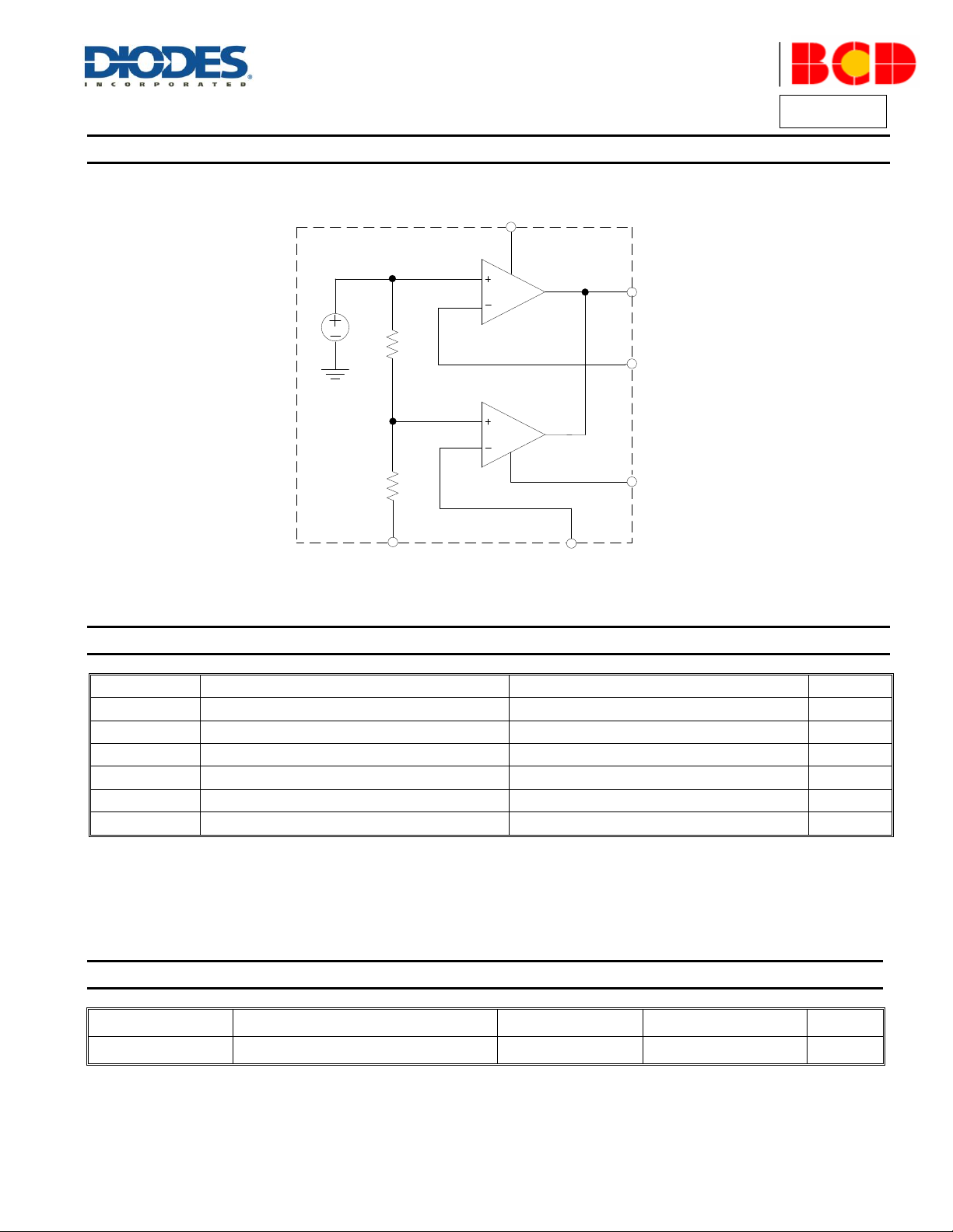
V
CC
V
OUT
V
CTRL
GND
V
SENSE
I
CTRL
4
5
2
1
3
6
1.210V
Symbol
Parameter
Rating
Unit
VCC
Power Supply Voltage
20
V
VIN
Input Voltage
-0.3 to VCC
V
TJ
Junction Temperature
+150
C
T
STG
Storage Temperature
-65 to +150
C
T
LEAD
Lead Temperature (Soldering, 5sec)
+260
C
θ
JA
Thermal Resistance (Junction to Ambient)
250
C/W
Symbol
Parameter
Min
Max
Unit
VCC
Power Supply Voltage
1.7
18
V
Functional Block Diagram
Absolute Maximum Ratings (Note 4)
Note 4: Stresses greater than those listed under “Absolute Maximum Ratings” may cause permanent damage to the device. These are stress ratings only, and
functional operation of the device at these or any other conditions beyond those indicated under “Recommended Operating Conditions” is not implied.
Exposure to “Absolute Maximum Ratings” for extended periods may affect device reliability.
Recommended Operating Conditions
Page 5
AP4312
Document number: DS36797 Rev. 1 - 2
5 of 11
www.diodes.com
January 2014
© Diodes Incorporated
AP4312
A Product Line of
Diodes Incorporated
Symbol
Parameters
Conditions
Min
Typ
Max
Unit
TOTAL CURRENT CONSUMPTION
I
CC
Total Supply Current Not Including the
Output Sinking Current
TA=+25C
–
180
–
μA
-40C <TA<+105C
– – 300
VOLTAGE CONTROL LOOP
Gmv
Transconductance of Voltage Control
Loop Op-Amp
(Sink Current Only)
TA=+25C
1
3.5
–
mA/mV
-40C <TA<+105C
–
2.5
–
V
REF
Voltage Control Loop Reference
TA=+25C
1.204
1.21
1.216
V
-40C <TA<+105C
1.186
1.234
I
IBV
Input Bias Current (V
CTRL
)
TA=+25C
–
50
–
nA
-40C <TA<+105C
–
100
–
CURRENT CONTROL LOOP
Gmi
Transconductance of Current Control
Loop Op-Amp
(Sink Current Only)
TA=+25C
1.5 7 –
mA/mV
-40C <TA<+105C
1.5 7 –
V
SENSE
Current Control Loop Reference
TA=+25C
67.9
70
72.1
mV
-40C <TA<+105C
66
74
I
IBI
Current Out of Pin I
CTRL
at V
SENSE
TA=+25C
–
18
–
μA
-40C <TA<+105C
–
35
–
OUTPUT STAGE
V
OL
Low Output Voltage Level
TA=+25C, I
SINK
=2mA
–
100
–
mV
-40C <TA<+105C, I
SINK
=2mA
–
100
–
I
OS
Output Short Circuit Current.
Output to V
CC.
Sink Current Only
TA=+25C
–
27
50
mA
-40C <TA<+105C
–
35
–
Symbol
Parameter
Value
Unit
θ
JC
Thermal Resistance (Junction to Case)
84
C/W
Electrical Characteristics (@V
=5V, TA=+25C, unless otherwise specified.)
CC
Thermal Impedance
Page 6
AP4312
Document number: DS36797 Rev. 1 - 2
6 of 11
www.diodes.com
January 2014
© Diodes Incorporated
AP4312
A Product Line of
Diodes Incorporated
-20 0 20 40 60 80 100 120
1.190
1.195
1.200
1.205
1.210
1.215
1.220
1.225
1.230
VCC=1.7V
VCC=5V
VCC=18V
V
REF
(V)
Ambient Temperature ( oC )
-40 -20 0 20 40 60 80 100 120 140
66
67
68
69
70
71
72
73
74
V
SENSE
(mV)
Ambient Temperature (oC)
VCC=1.7V
VCC=5V
VCC=18V
-20 0 20 40 60 80 100 120
0
10
20
30
40
50
Ambient Temperature ( oC )
I
IBV
(nA)
VCC=1.7V
VCC=5V
VCC=18V
-20 0 20 40 60 80 100 120
10
12
14
16
18
20
22
24
Ambient Temperature ( oC )
I
IBI
(A)
VCC=1.7V
VCC=5V
VCC=18V
-20 0 20 40 60 80 100 120
0
1
2
3
4
5
6
7
8
Ambient Temperature ( oC )
Gmv (mA/mV)
VCC=1.7V
VCC=5V
VCC=18V
-20 0 20 40 60 80 100 120
0
1
2
3
4
5
6
7
8
9
10
11
12
13
14
15
16
17
18
19
20
Ambient Temperature ( oC )
Gmi (mA/mV)
VCC=1.7V
VCC=5V
VCC=18V
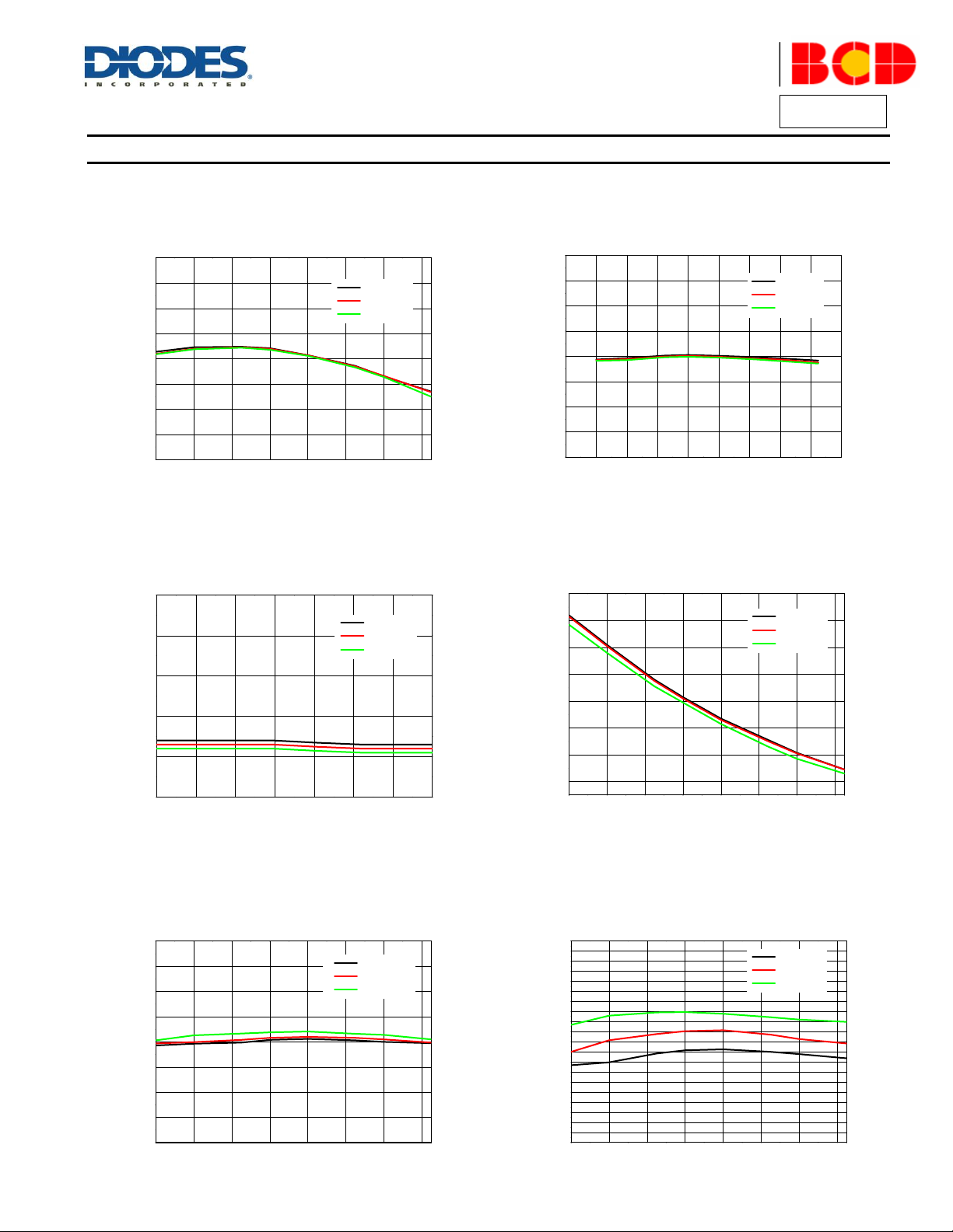
Performance Characteristics
Voltage Control Loop Reference Current Control Loop Reference
vs. Ambient Temperature vs. Ambient Temperature
Input Bias Current (V
vs. Ambient Temperature vs. Ambient Temperature
Transconductance of Voltage Control Loop Transconductance of Current Control Loop
Op-Amp vs. Ambient Temperature Op-Amp vs. Ambient Temperature
) Current Out of Pin I
CTRL
CTRL
at V
SENSE
Page 7
AP4312
Document number: DS36797 Rev. 1 - 2
7 of 11
www.diodes.com
January 2014
© Diodes Incorporated
AP4312
A Product Line of
Diodes Incorporated
-20 0 20 40 60 80 100 120
0
10
20
30
40
50
Ambient Temperature ( oC )
V
OLV
(mV)
VCC=1.7V
VCC=5V
VCC=18V
-20 0 20 40 60 80 100 120
0
10
20
30
40
50
Ambient Temperature ( oC )
V
OLC
(mV)
VCC=1.7V
VCC=5V
VCC=18V
-20 0 20 40 60 80 100 120
0
10
20
30
40
50
60
70
Ambient Temperature ( oC )
I
OSV
(mA)
VCC=1.7V
VCC=5V
VCC=18V
-20 0 20 40 60 80 100 120
0
10
20
30
40
50
60
70
Ambient Temperature ( oC )
I
OSC
(mA)
VCC=1.7V
VCC=5V
VCC=18V
-20 0 20 40 60 80 100 120
0
50
100
150
200
250
300
Ambient Temperature ( oC )
I
CC
(A)
VCC=1.7V
VCC=5V
VCC=18V
0 5 10 15 20 25 30 35
0
100
200
300
400
500
600
700
800
V
OL
(mV)
Sink Current (mA)
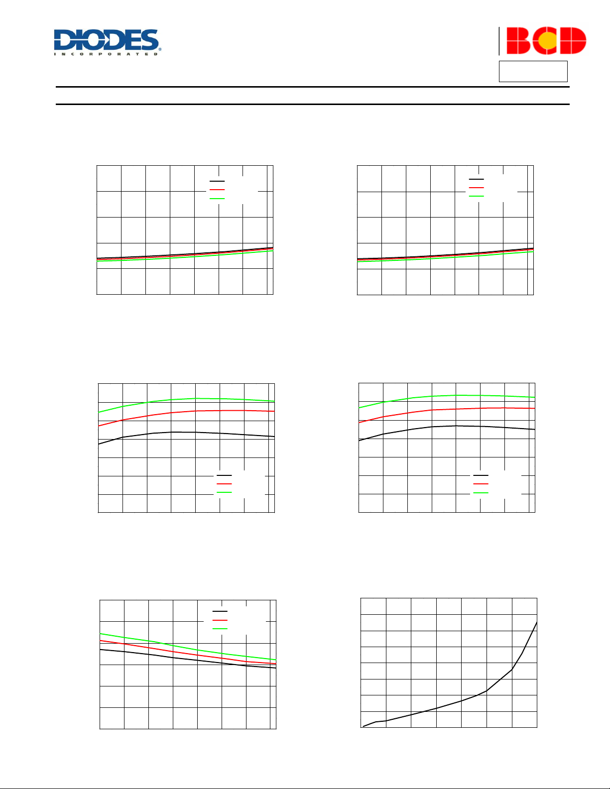
Performance Characteristics (Cont.)
Low Output Level of Voltage Control Loop Low Output Level of Current Control Loop
Op-Amp vs. Ambient Temperature Op-Amp vs. Ambient Temperature
Output Short Circuit Current of Voltage Control Output Short Circuit Current of Current Control
Loop Op-Amp vs. Ambient Temperature Loop Op-Amp vs. Ambient Temperature
Total Supply Current Not Including the Low Output Voltage Level vs. Sink Current
Output Sinking Current vs. Ambient Temperature
Page 8

AP4312
Document number: DS36797 Rev. 1 - 2
8 of 11
www.diodes.com
January 2014
© Diodes Incorporated
AP4312
A Product Line of
Diodes Incorporated
AP4312 XX XX - G1
Packing
Package
TR : Tape & Reel
K6 : SOT26
G1 : Green
Product Name
RoHS/Green
Package
Part Number
Marking ID
Packing
SOT26
AP4312K6TR-G1
GKD
3000/Tape & Reel
: Logo
XXX: Marking ID (See ordering information)
Ordering Information
Diodes IC’s Pb-free products with "G1" suffix in the part number, are RoHS compliant and green.
Marking Information
Page 9
AP4312
Document number: DS36797 Rev. 1 - 2
9 of 11
www.diodes.com
January 2014
© Diodes Incorporated
AP4312
A Product Line of
Diodes Incorporated
2.820(0.111)
3.100(0.122)
2.650(0.104)
3.000(0.118)
1.500(0.059)
1.700(0.067)
0.950(0.037)TYP
1.800(0.071)
2.000(0.079)
0.300(0.012)
0.500(0.020)
0.700(0.028)REF
0.100(0.004)
0.200(0.008)
0°
8°
0.200(0.008)
0.300(0.012)
0.600(0.024)
0.000(0.000)
0.150(0.006)
0.900(0.035)
1.300(0.051)
1.450(0.057)
MAX
1 2 3
4
5
6
Pin 1 Mark
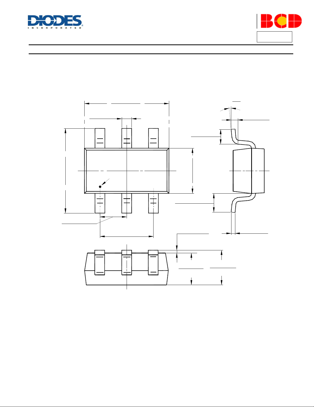
Package Outline Dimensions (All dimensions in mm(inch).)
(1) Package Type: SOT26
Page 10

AP4312
Document number: DS36797 Rev. 1 - 2
10 of 11
www.diodes.com
January 2014
© Diodes Incorporated
AP4312
A Product Line of
Diodes Incorporated
E E
G
Z
Y
X
Dimensions
Z
(mm)/(inch)
G
(mm)/(inch)
X
(mm)/(inch)
Y
(mm)/(inch)
E
(mm)/(inch)
Value
3.600/0.142
1.600/0.063
0.700/0.028
1.000/0.039
0.950/0.037
Suggested Pad Layout
(1) Package Type: SOT26
Page 11
AP4312
Document number: DS36797 Rev. 1 - 2
11 of 11
www.diodes.com
January 2014
© Diodes Incorporated
AP4312
A Product Line of
Diodes Incorporated
DIODES INCORPORATED MAKES NO WARRANTY OF ANY KIND, EXPRESS OR IMPLIED, WITH REGARDS TO THIS DOCUMENT,
INCLUDING, BUT NOT LIMITED TO, THE IMPLIED WARRANTIES OF MERCHANTABILITY AND FITNESS FOR A PARTICULAR PURPOSE
(AND THEIR EQUIVALENTS UNDER THE LAWS OF ANY JURISDICTION).
Diodes Incorporated and its subsidiaries reserve the right to make modifications, enhancements, improvements, corrections or other changes
without further notice to this document and any product described herein. Diodes Incorporated does not assume any liability arising out of the
application or use of this document or any product described herein; neither does Diodes Incorporated convey any license under its patent or
trademark rights, nor the rights of others. Any Customer or user of this document or products described herein in such applications shall assume
all risks of such use and will agree to hold Diodes Incorporated and all the companies whose products are represented on Diodes Incorporated
website, harmless against all damages.
Diodes Incorporated does not warrant or accept any liability whatsoever in respect of any products purchased through unauthorized sales channel.
Should Customers purchase or use Diodes Incorporated products for any unintended or unauthorized application, Customers shall indemnify and
hold Diodes Incorporated and its representatives harmless against all claims, damages, expenses, and attorney fees arising out of, directly or
indirectly, any claim of personal injury or death associated with such unintended or unauthorized application.
Products described herein may be covered by one or more United States, international or foreign patents pending. Product names and markings
noted herein may also be covered by one or more United States, international or foreign trademarks.
This document is written in English but may be translated into multiple languages for reference. Only the English version of this document is the
final and determinative format released by Diodes Incorporated.
Diodes Incorporated products are specifically not authorized for use as critical components in life support devices or systems without the express
written approval of the Chief Executive Officer of Diodes Incorporated. As used herein:
A. Life support devices or systems are devices or systems which:
1. are intended to implant into the body, or
2. support or sustain life and whose failure to perform when properly used in accordance with instructions for use provided in the
labeling can be reasonably expected to result in significant injury to the user.
B. A critical component is any component in a life support device or system whose failure to perform can be reasonably expected to cause the
failure of the life support device or to affect its safety or effectiveness.
Customers represent that they have all necessary expertise in the safety and regulatory ramifications of their life support devices or systems, and
acknowledge and agree that they are solely responsible for all legal, regulatory and safety-related requirements concerning their products and any
use of Diodes Incorporated products in such safety-critical, life support devices or systems, notwithstanding any devices- or systems-related
information or support that may be provided by Diodes Incorporated. Further, Customers must fully indemnify Diodes Incorporated and its
representatives against any damages arising out of the use of Diodes Incorporated products in such safety-critical, life support devices or systems.
Copyright © 2013, Diodes Incorporated
www.diodes.com
IMPORTANT NOTICE
LIFE SUPPORT
 Loading...