

Page 1
AP4310E
Document number: DS36787 Rev. 2 - 2
1 of 9
www.diodes.com
December 2013
© Diodes Incorporated
AP4310E
A Product Line of
Diodes Incorporated
Description
The AP4310E is a monolithic IC specifically designed to regulate the
output current and voltage levels of switching battery chargers and
power supplies
The device contains two Op Amps and a 2.5V precision shunt voltage
reference. Op Amp 1 is designed for voltage control with its noninverting input internally connected to the output of the shunt
regulator. Op Amp 2 is for current control with both inputs
uncommitted. The IC offers the power converter designer a control
solution that features increased precision with a corresponding
reduction in system complexity and cost. AP4310E has more
stringent reference voltage tolerance and offset.
The AP4310E is available in standard package of SO-8.
Applications
Battery Charger
Switching Power Supply
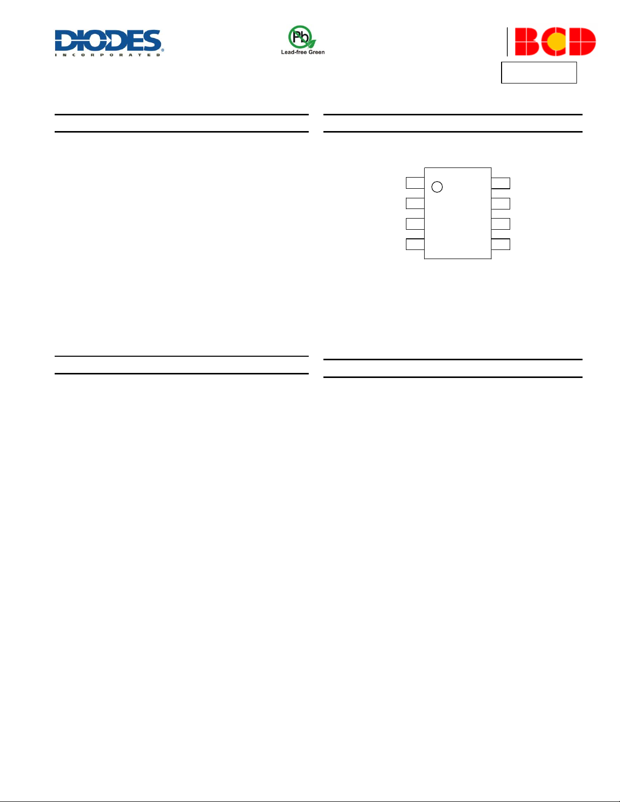
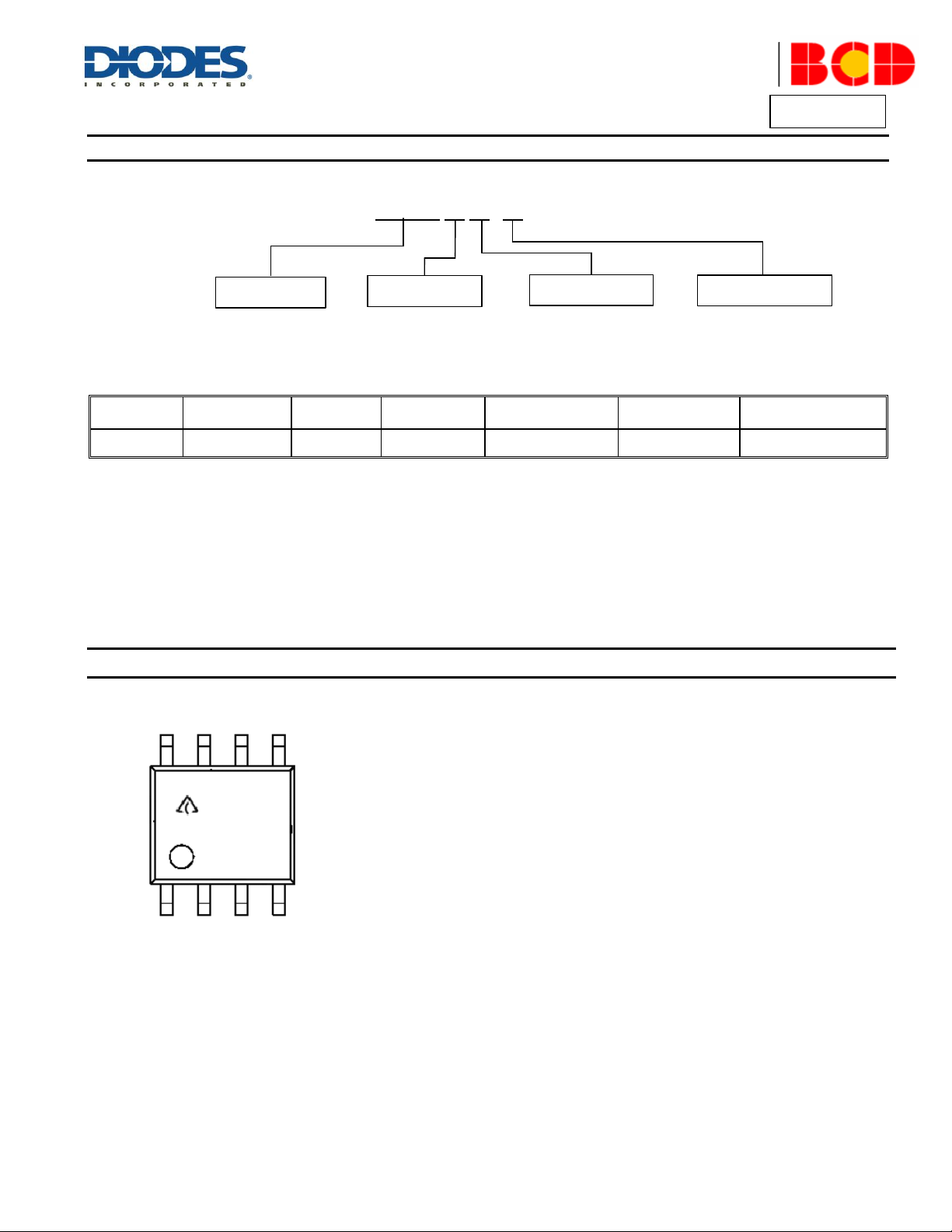
Pin Assignments
(Top View)
1
2
3
4
8
7
6
5
OUTPUT 1
INPUT 1-
INPUT 1+/VKA
GND
INPUT 2-
INPUT 2+
OUTPUT 2
VCC
SO-8 (M Package)
Features
OP Amp
Input Offset Voltage: 0.5mV
Supply Current: 75A per OP Amp at 5.0V Supply Voltage
Unity Gain Bandwidth:1MHz
Output Voltage Swing: 0 to VCC-1.5V
Power Supply Range: 3 to 36V
Voltage Reference
Fixed Output Voltage Reference: 2.5V
Reference Voltage Tolerance: ±0.4%
Sink Current Capability: 0.05 to 80mA
Typical Output Impedance: 0.2Ω
Totally Lead-free & Fully RoHS Compliant (Note1 & 2)
Halogen and Antimony Free. “Green” Device (Note 3)
Notes: 1. No purposely added lead. Fully EU Directive 2002/95/EC (RoHS) & 2011/65/EU (RoHS 2) compliant.
2. See http://www.diodes.com/quality/lead_free.html for more information about Diodes Incorporated’s definitions of Halogen- and Antimony-free, "Green"
and Lead-free.
3. Halogen- and Antimony-free "Green” products are defined as those which contain <900ppm bromine, <900ppm chlorine (<1500ppm total Br + Cl) and
<1000ppm antimony compounds.
DUAL OP AMP AND VOLTAGE REFERENCE
Page 2
AP4310E
Document number: DS36787 Rev. 2 - 2
2 of 9
www.diodes.com
December 2013
© Diodes Incorporated
AP4310E
A Product Line of
Diodes Incorporated
AC
Line
SMPS
R2
Current
Sense
R7
R8
Battery Pack
R4
R3
R5
R6
R1
Opto
Isolator
+
-
Op Amp 2
+
-
Op Amp 1
AP4310E
OUTPUT 1
INPUT 1-
INPUT 1+/VKA
GND
VCC
OUTPUT 2
INPUT 2-
INPUT 2+
-
+
-
+
1
2
3
4
8
7
6
5
Op
Amp 1
Op
Amp 2
Typical Applications Circuit
Functional Block Diagram
Application of AP4310E in a Constant Current and Constant Voltage Charger
Page 3
AP4310E
Document number: DS36787 Rev. 2 - 2
3 of 9
www.diodes.com
December 2013
© Diodes Incorporated
AP4310E
A Product Line of
Diodes Incorporated
Symbol
Parameter
Rating
Unit
VCC
Power Supply Voltage (VCC to GND)
40
V
VIN
Op Amp1 and 2 Input Voltage Range (Pins 2, 5, 6)
-0.3 to VCC+0.3
V
VID
Op Amp 2 Input Differential Voltage (Pins 5, 6)
40
V
IK
Voltage Reference Cathode Current (Pin 3)
100
mA
PD
Power Dissipation (TA=+25°C )
500
mW
TJ
Operating Junction Temperature
+150
C
T
STG
Storage Temperature Range
-65 to +150
C
T
LEAD
Lead Temperature (Soldering 10sec)
+260
C
Parameter
Min
Max
Unit
Supply Voltage
3
36
V
Ambient Temperature
-40
+105
C
Parameters
Conditions
Min
Typ
Max
Unit
Total Supply Current, excluding Current in
Voltage Reference
VCC=5V, no load, -40°C≤TA≤+105°C
–
0.15
0.25
mA
VCC=30V, no load, -40°C≤TA ≤+105°C
–
0.20
0.30
Voltage Reference Section
Reference Voltage
IK=10mA
TA=+25°C
2.49
2.50
2.51
V
-40°C≤TA ≤+105°C
2.48
2.50
2.52
Reference Voltage Deviation over Full
Temperature Range
IK=10mA, TA=-40°C to +105°C
–
5
24
mV
Minimum Cathode Current for Regulation
–
–
0.01
0.05
mA
Dynamic Impedance
IK=1mA to 80mA, f<1kHz
–
0.2
0.5
Ω
Op Amp 1 Section (VCC=5V, VO=1.4V, TA=+25°C, unless otherwise noted.)
Input Offset Voltage
TA=+25°C
–
0.5
3
mV
TA=-40°C to +105°C
–
–
5
Input Offset Voltage Temperature Drift
TA=-40°C to +105°C
–
7 – μV/°C
Input Bias Current (Inverting Input Only)
TA=+25°C
–
20
150
nA
Large Signal Voltage Gain
VCC=15V, RL=2kΩVO=1.4V to 11.4V
85
100 – dB
Power Supply Rejection Ratio
VCC=5V to 30V
70
90 – dB
Absolute Maximum Ratings (Note 4)
Note 4: Stresses greater than those listed under “Absolute Maximum Ratings” may cause permanent damage to the device. These are str ess ratings only, and
functional operation of the device at these or any other conditions beyond those indicated under “Recommended Operating Conditions” is not implied.
Exposure to “Absolute Maximum Ratings” for extended periods may affect device reliability.
Recommended Operating Conditions (Note 5)
Note 5: Qualified for SMD on the underside of a PCB by processing the PCB through a wave soldering operation.
Electrical Characteristics (@V
=5V, TA=+25C, unless otherwise specified.)
CC
Page 4

AP4310E
Document number: DS36787 Rev. 2 - 2
4 of 9
www.diodes.com
December 2013
© Diodes Incorporated
AP4310E
A Product Line of
Diodes Incorporated
Parameters
Conditions
Min
Typ
Max
Unit
Output Current
Source
V
CC
= 15V, VID=1VVO = 2V
20
40
–
mA
Sink
V
CC
= 15V, V
ID
= -1VVO = 2V
8
20
–
Output Voltage Swing (High)
V
CC
= 30V, RL = 10kΩV
ID
= 1V
27
28 – V
Output Voltage Swing (Low)
V
CC
= 30V, RL = 10kΩV
ID
= -1V
–
17
100
mV
Slew Rate
V
CC
= 18V, RL = 2kΩAV = 1,
V
IN
= 0.5V to 2V, CL = 100pF
0.2
0.5 – V/μs
Unity Gain Bandwidth
V
CC
= 30V, RL = 2kΩCL = 100pF
0.7
1.0 – MHz
Op Amp 2 Section (VCC= 5V, VO=1.4V, TA =+25°C, unless otherwise noted.)
Input Offset Voltage (Note 6)
TA = +25°C, V
CC
= 5V or 20V
–
0.5
2
mV
TA = -40°C to +105°C, V
CC
= 5V or 20V
– – 3
Input Offset Voltage Temperature Drift
TA = -40°C to +105°C
– 7 –
μV/°C
Input Offset Current
TA = +25°C
– 2 30
nA
Input Bias Current
TA = +25°C
–
20
150
nA
Input Voltage Range
V
CC
= 0 to 36V
0
–
VCC-1.5
V
Common Mode Rejection Ratio
TA = +25°C, V
CM
= 0 to 3.5V
70
85 – dB
Large Signal Voltage Gain
V
CC
= 15V, RL = 2kΩVO = 1.4V to 11.4V
85
100 – dB
Power Supply Rejection Ratio
V
CC
= 5V to 30V
70
90 – dB
Output Current
Source
V
CC
= 15V, V
ID
= 1VVO = 2V
20
40
–
mA
Sink
V
CC
= 15V, V
ID
= -1VVO = 2V
8
20
–
Output Voltage Swing (High)
V
CC
= 30V, RL = 10kΩV
ID
= 1V
27
28 – V
Output Voltage Swing (Low)
V
CC
= 30V, RL = 10kΩV
ID
= -1V
–
17
100
mV
Slew Rate
V
CC
= 18V, RL = 2kΩAV = 1,
V
IN
= 0.5V to 2V, CL = 100pF
0.2
0.5 – V/μs
Unity Gain Bandwidth
V
CC
= 30V, RL = 2kΩCL = 100pF
0.7
1.0 – MHz
Electrical Characteristics (Cont.) (@V
=5V, TA=+25C, unless otherwise specified.)
CC
Note 6: The full temperature feature is guaranteed by design.
Page 5
AP4310E
Document number: DS36787 Rev. 2 - 2
5 of 9
www.diodes.com
December 2013
© Diodes Incorporated
AP4310E
A Product Line of
Diodes Incorporated
-40 -20 0 20 40 60 80 100 120
2.480
2.485
2.490
2.495
2.500
2.505
2.510
Reference Voltage (V)
Ambient Temperature (oC)
-2 -1 0 1 2 3
-100
-50
0
50
100
150
Cathode Current (mA)
Cathode Voltage (V)
VKA=V
REF
TA=250C
-40 -20 0 20 40 60 80 100 120
0
5
10
15
20
25
30
Input Bias Current (nA)
Ambient Temperature (oC)
0 2 4 6 8 10 12 14 16 18 20
60
70
80
90
100
110
Voltage Gain(dB)
Supply Voltage (V)
RL=2K
RL=20K
Performance Characteristics
Reference Voltage vs. Ambient Temperature Cathode Current vs. Cathode Voltage
Input Bias Current vs. Ambient Temperature Op Amp Voltage Gain
Page 6
AP4310E
Document number: DS36787 Rev. 2 - 2
6 of 9
www.diodes.com
December 2013
© Diodes Incorporated
AP4310E
A Product Line of
Diodes Incorporated
AP4310E XX XX - G1
Packing
Package
TR : Tape & Reel
M: SO-8
G1 : Green
RoHS/Green
Product Name
Package
Temperature
Range
Reference
Voltage
Voltage
Tolerance
Part Number
Marking ID
Packing Type
SO-8
-40 to +105°C
2.5V
±0.4%
AP4310EMTR-G1
AP4310EM-G1
4000/Tape & Reel
First and Second Lines: Logo and Marking ID
(See Ordering Information)
Third Line: Date Code
Y: Year
WW: Work Week of Molding
A: Assembly House Code
XX: 7th and 8th Digits of Batch No.
AP4310
EM-G1
YWWAXX
Ordering Information
Diodes IC’s Pb-free products with "G1" suffix in the part number, are RoHS compliant and green.
Marking Information
Page 7
AP4310E
Document number: DS36787 Rev. 2 - 2
7 of 9
www.diodes.com
December 2013
© Diodes Incorporated
AP4310E
A Product Line of
Diodes Incorporated
0
°
8
°
1
°
7
°
R
0
.
1
5
0
(
0
.
0
0
6
)
R0.150(0.006)
1.000(0.039)
0.300(0.012)
0.510(0.020)
1.350(0.053)
1.750(0.069)
0.100(0.004)
0.300(0.012)
3.800(0.150)
4.000(0.157)
7
°
7
°
20:
1
D
1.270(0.050)
TYP
0.150(0.006)
0.250(0.010)
8
°
D
5.800(0.228)
6.200(0.244)
0.600(0.024)
0.725(0.029)
0.320(0.013)
8
°
0.450(0.017)
0.820(0.032)
4.700(0.185)
5.100(0.201)
Note: Eject hole, oriented hole and mold mark is optional
.
Option 1
Option 1
Option 2
0.
350
(0.014)
TYP
TYP
TYP
9
°
~
9
°
~
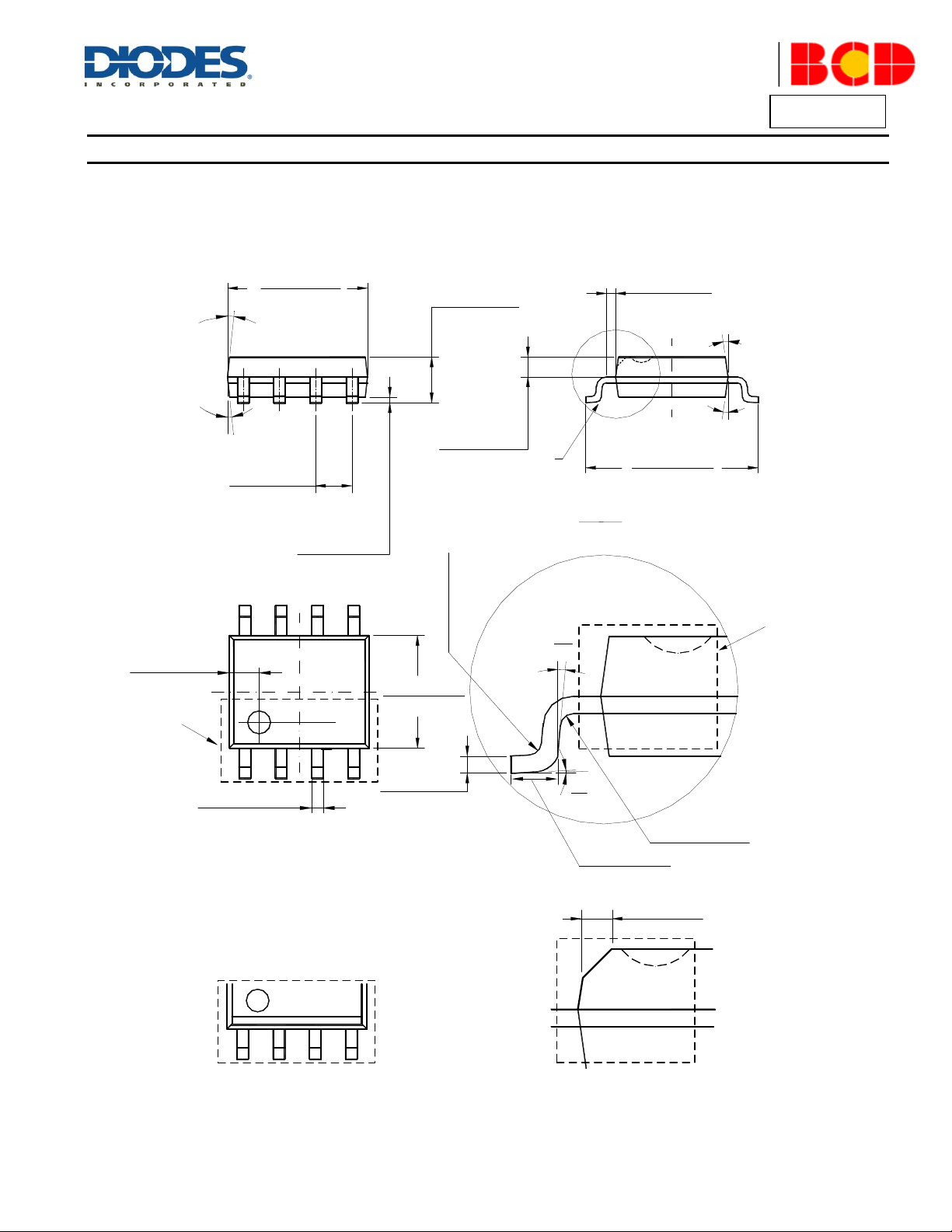
Package Outline Dimensions (All dimensions in mm (inch).)
(1) Package Type: SO-8
Page 8
AP4310E
Document number: DS36787 Rev. 2 - 2
8 of 9
www.diodes.com
December 2013
© Diodes Incorporated
AP4310E
A Product Line of
Diodes Incorporated
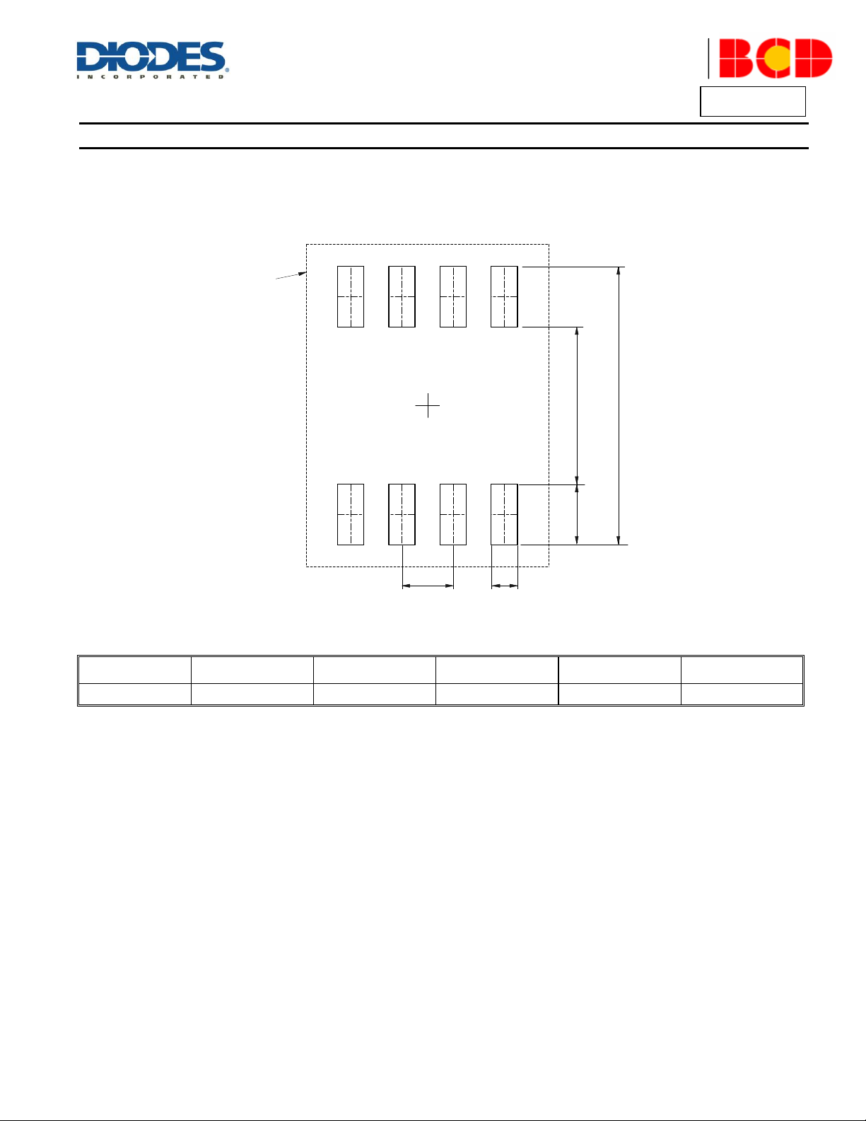
Grid
placement
courtyard
ZG
Y
E X
Dimensions
Z
(mm)/(inch)
G
(mm)/(inch)
X
(mm)/(inch)
Y
(mm)/(inch)
E
(mm)/(inch)
Value
6.900/0.272
3.900/0.154
0.650/0.026
1.500/0.059
1.270/0.050
Suggested Pad Layout
(1) Package Type: SO-8
Page 9

AP4310E
Document number: DS36787 Rev. 2 - 2
9 of 9
www.diodes.com
December 2013
© Diodes Incorporated
AP4310E
A Product Line of
Diodes Incorporated
DIODES INCORPORATED MAKES NO WARRANTY OF ANY KIND, EXPRESS OR IMPLIED, WITH REGARDS TO THIS DOCUMENT,
INCLUDING, BUT NOT LIMITED TO, THE IMPLIED WARRANTIES OF MERCHANTABILITY AND FITNESS FOR A PARTICULAR PURPOSE
(AND THEIR EQUIVALENTS UNDER THE LAWS OF ANY JURISDICTION).
Diodes Incorporated and its subsidiaries reserve the right to make modifications, enhancements, improvements, corrections or other changes
without further notice to this document and any product described herein. Diodes Incorporated does not assume any liability arising out of the
application or use of this document or any product described herein; neither does Diodes Incorporated convey any license under its patent or
trademark rights, nor the rights of others. Any Customer or user of this document or products described herein in such applications shall assume
all risks of such use and will agree to hold Diodes Incorporated and all the companies whose products are represented on Diodes Incorporated
website, harmless against all damages.
Diodes Incorporated does not warrant or accept any liability whatsoever in respect of any products purchased through unauthorized sales channel.
Should Customers purchase or use Diodes Incorporated products for any unintended or unauthorized application, Customers shall indemnify and
hold Diodes Incorporated and its representatives harmless against all claims, damages, expenses, and attorney fees arising out of, directly or
indirectly, any claim of personal injury or death associated with such unintended or unauthorized application.
Products described herein may be covered by one or more United States, international or foreign patents pending. Product names and markings
noted herein may also be covered by one or more United States, international or foreign trademarks.
This document is written in English but may be translated into multiple languages for reference. Only the English version of this document is the
final and determinative format released by Diodes Incorporated.
Diodes Incorporated products are specifically not authorized for use as critical components in life support devices or systems without the express
written approval of the Chief Executive Officer of Diodes Incorporated. As used herein:
A. Life support devices or systems are devices or systems which:
1. are intended to implant into the body, or
2. support or sustain life and whose failure to perform when properly used in accordance with instructions for use provided in the
labeling can be reasonably expected to result in significant injury to the user.
B. A critical component is any component in a life support device or system whose failure to perform can be reasonably expected to cause the
failure of the life support device or to affect its safety or effectiveness.
Customers represent that they have all necessary expertise in the safety and regulatory ramifications of their life support devices or systems, and
acknowledge and agree that they are solely responsible for all legal, regulatory and safety-related requirements concerning their products and any
use of Diodes Incorporated products in such safety-critical, life support devices or systems, notwithstanding any devices- or systems-related
information or support that may be provided by Diodes Incorporated. Further, Customers must fully indemnify Diodes Incorporated and its
representatives against any damages arising out of the use of Diodes Incorporated products in such safety-critical, life support devices or systems.
Copyright © 2013, Diodes Incorporated
www.diodes.com
IMPORTANT NOTICE
LIFE SUPPORT
 Loading...