

Diodes AP3983R, APR3415B User Manual

10W Cost-Effective Charge AP3983R + APR3415B
EV1 Evaluation Board User Guide
Contents
Chapter 1. Summary ................................................................................................................. 2
1.1 General Description .......................................................................................................................... 2
1.2 Key Features .................................................................................................................................... 2
1.3 Applications ...................................................................................................................................... 2
1.4 Main Power Specifications (CV & CC Mode) ................................................................................... 2
1.5 Evaluation Board Picture: ................................................................................................................. 2
Chapter 2. Power Supply Specification .................................................................................. 3
2.1 Specification and Test Results ......................................................................................................... 3
2.1 Transformer Specification ................................................................................................................. 4
Chapter 3. Schematic ............................................................................................................... 5
3.1 Evaluation Board Schematic ............................................................................................................ 5
3.2 Bill of Material (BOM) ....................................................................................................................... 6
Chapter 4. The Evaluation Board (EVB) Connections ........................................................... 7
4.1 Evaluation Board PCB Layout .......................................................................................................... 7
4.2 Quick Start Guide Before Connection .............................................................................................. 7
Chapter 5. Testing the Evaluation Board ................................................................................ 8
5.1 Input & Output Characteristics ............................................................................... 8
5.1.1 Input Standby Power .................................................................................................. 8
5.1.2 Input Power Efficiency at Different Loading ............................................................... 8
5.1.3 OCP Current set point with at different AC line ......................................................... 9
5.1.4 PSU Output Characteristics: ...................................................................................... 9
5.2 Key Performance Waveforms: ............................................................................... 9
5.2.1 System start - up time ................................................................................................ 9
The system voltage stress on U2 D-S .............................................................................. 10
5.2.3 System Output Ripple performance ......................................................................... 10
5.2.4 System Dynamic Response performance with Vout @ 0A-2A ................................ 11
5.3 Thermal Test data at room Temperature after running 1 hr ............................... 12
5.4.1 System EMI L - Line Scan Data @115Vac ............................................................ 12
5.4.2 System EMI N - Line Scan Data @ 115Vac ........................................................... 13
5.4.3 System EMI L - Line Scan Data @ 230Vac ............................................................ 13
5.4.4 System EMI N-Line Scan Data @230Vac ............................................................. 14
AP3983R+ARP3415B Charger EV1 Page 1 of 15 3/1/2018
Rev 1.0 www.diodes.com

EV1 Evaluation Board User Guide
90 ~264VAC input range
Primary side regulation without an Opto-coupler.
Co-package PSR controller with 700V MOS die in
SO-7 Package
Multi-Mode PFM method operations, the switching
frequency between 24Khz and 80Khz.
With Valley-on detection for switching at Valley-on
region to improve power converting efficiency & EMI
performance.
Burst mode operation and low start-up operating
quiescent current to achieve 75mW low standby
power.
Three-mode operation to provide accurate constant
voltage (CV) regulation & constant current (CC)
performance.
Soft start during startup process and built-in Jittering
Frequency function to improve EMI emission.
Internal Auto Recovery OCP, OVP, OLP, OTP Power
Protection, cycle by cycle current limit, also with DC
polarity protection
Built–in Cable Compensation mode.
Brown out Protection.
1.2.2 APR3415B
Synchronous rectification of DCM Operation
Co-package 50V 17mΩ Rdson MOS die with SR
Controller in SO-8 package
Eliminate resonant ring interference
Fast detection of supply voltage
Minimum supporting components
Parameter
Value
Input Voltage
90 to 264VAC
Input standby power
75mW
Main output Vo / Io
5V – 2.0A
Efficiency
~ 85%
Total Output Power
10W
Protections
OCP, OVP, OLP,OTP
XYZ Dimension
29 x 32 x 15 mm
ROHS Compliance
Yes
Chapter 1. Summary
1.1 General Description
Based on Primary Side Regulation (PSR) Flyback
topology, the 10W Charger EV1 Evaluation board is
designed as an MP-form-factor, cost-effective, optimal
efficiency, charger reference design to facilitate further
customization by users. AP3983R PSR Switcher, copackaged a 700V N-MOSFE and a PSR control die, along
with APR3415B Synchronous Rectification (SR) Switcher,
co-packaged a MOS die with an SR controller, enable
high-efficiency and small size form-factor 10W charger
designs. The overall efficiency of the evaluation board
can meet DOE VI and CoC Tier 2 energy efficiency
requirements.
1.2 Key Features
1.2.1 AP3983R
1.5 Evaluation Board Picture:
1.3 Applications
Switching AC-DC Adaptors & Chargers
Home Appliances system powers
Auxiliary Vcc power supply for large power systems
1.4 Main Power Specifications (CV & CC Mode)
AP3983R+ARP3415B Charger EV1 Page 2 of 15 3/1/2018
Rev 1.0 www.diodes.com
Figure 1: Top View
Figure 2: Bottom View
10W Cost-Effective Charge AP3983R + APR3415B
EV1 Evaluation Board User Guide
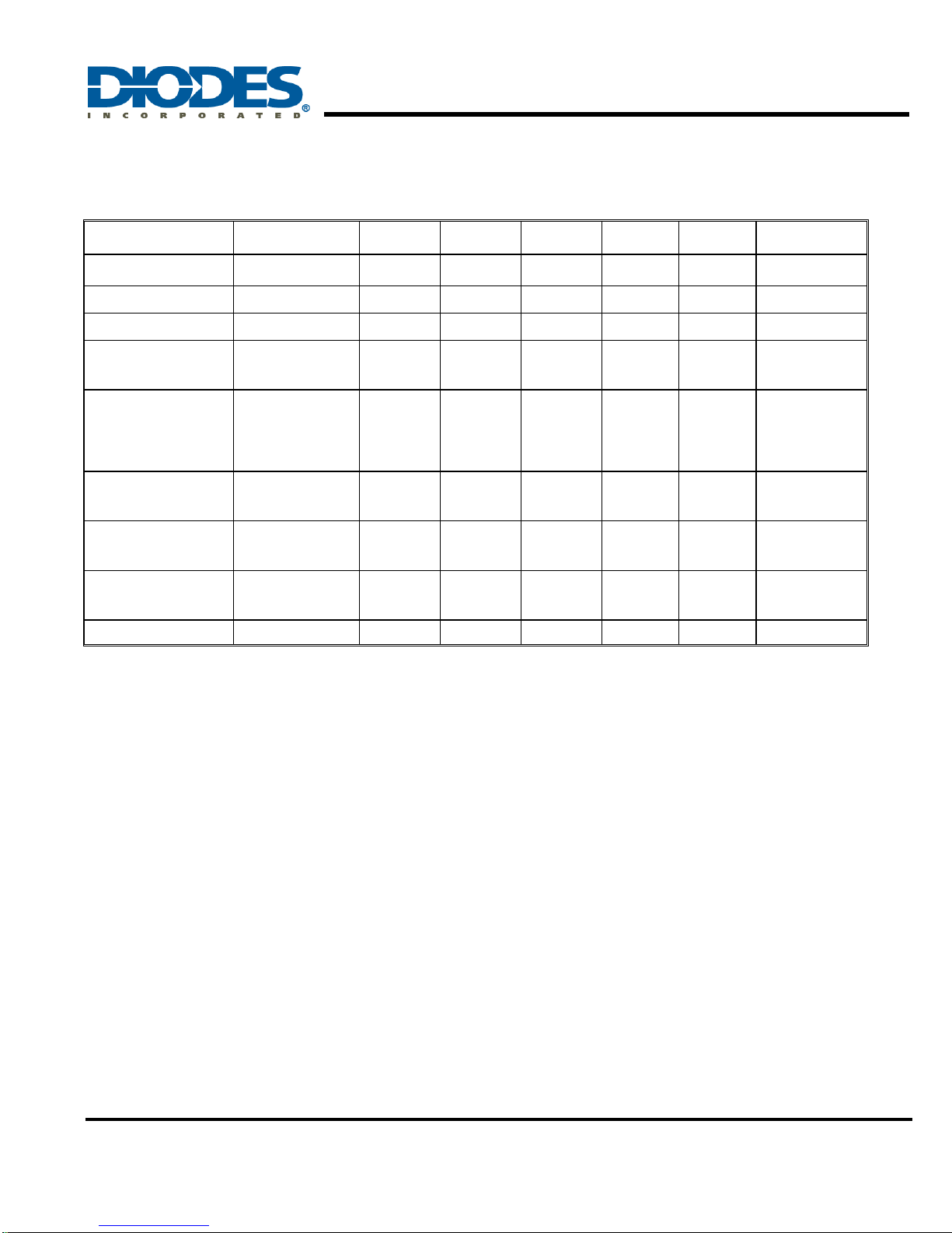
Parameter
Test conditions
Min
Nom
Max
Eff /DOE
Level VI
Eff /CoC
V5 Tier2
Test
Summary
V
ACIN
Input Voltage
-
90 V
RMS
115/230
264 V
RMS
- - -
F
LINE
Frequency
-
47Hz
50/60
64Hz - -
-
IIN Input Current
- - -
0.23 A
RMS
- - Pass
No load Pin
At 230Vac/50Hz,
@ 5V,
Pin < 75mW
- - 75mW - -
Pass,
230Vac:
46mW
5VDC / 2A
@115Vac/230Vac
Average efficiency
Board end
-
5V/2A
-
78.7%
Pass,
115Vac:
84.65%
230Vac:
84.39%
Thermal
Performance
5V-2A
@ 90Vac
AP3983R
IC =86.4C
@85Vac
AP3983R
IC=88.0C
@264Vac
Pass
EMI Scan Data
5V-2A
@115Vac L & N
Under
Limit line
< -6db
Pass
5V-2A
@230Vac L & N
Under
Limit line
< -6db
Pass
Chapter 2. Power Supply Specification
2.1 Specification and Test Results
DoE VI Eff ≥ 0.0834xLn(Po)-0.0014xPo+0.609 <Vo<6V
DoE VI Eff ≥ 0.071xLn(Po)-0.0014xPo+0.67 Vo>6V
AP3983R+ARP3415B Charger EV1 Page 3 of 15 3/1/2018
Rev 1.0 www.diodes.com

10W Cost-Effective Charge AP3983R + APR3415B
EV1 Evaluation Board User Guide
EE16C (Ae = 19mm^2)
NO Winding
NAME
TERMINAL NO.
WINDING
START
FINISH
WIRE
TURNS
Layers
1
Np1 5 6
Φ 0.21mm
60Ts
3
2
Na 2 1
Φ 0.19mm x 2
11 Ts
1
3
Shield
1(GND)
NC
Φ 0.19mm x 1
8T
1
4
Ns
3(+)
4
Φ 0.7W x 1
4 Ts
1
Primary Inductance
Pin 5-6,all other windings open, measured at
1kHz, 0.4VRMS
1.05mH ± 7 %
Primary Leakage
Inductance
Pin 5-6, all other windings shorted, measured at
10kHz, 0.4VRMS
80 uH (Max.)
2.1 Transformer Specification
AP3983R (90 VAC ~ 265VAC one outputs 10W Transformer Spec.)
1) C o r e a n d Bobbin:
EE16C, 2+2+2 pin
2) Transformer Parameters
1. Primary Inductance (Pin5-Pin6), all other windings are open Lp =1.05mH
± 7
% @1KHz
AP3983R+ARP3415B Charger EV1 Page 4 of 15 3/1/2018
Rev 1.0 www.diodes.com
10W Cost-Effective Charge AP3983R + APR3415B
EV1 Evaluation Board User Guide
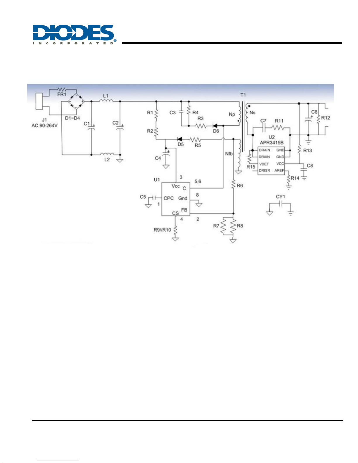
Chapter 3. Schematic
3.1 Evaluation Board Schematic
Figure 3: Evaluation Board Schematic
AP3983R+ARP3415B Charger EV1 Page 5 of 15 3/1/2018
Rev 1.0 www.diodes.com
 Loading...