

Page 1
Data Sheet
SIXTEEN-CHANNEL, 75mA CURRENT SINK WITH CURRENT MATCH AP3616
General Description
The AP3616 is an sixteen-channel constant current
sink with current match used for LED driver. It uses an
external resistor to set the current for sixteen LED
strings with an accuracy of ±1.5%. The full scale LED
current can be adjusted from 20mA to 75mA for each
channel. The LED lightness can be adjusted by PWM
dimming function.
The device can keep working normally without any
damage when LEDs are short or open. It features under
voltage lockout protection and over temperature protection.
The AP3616 has three interface terminals (FB, SYN
and FBX pins). The FB and SYN pins allow the device
to work with a DC/DC converter to drive LED arrays
for good performance. And the FBX pin enables the
device to be connected in parallel.
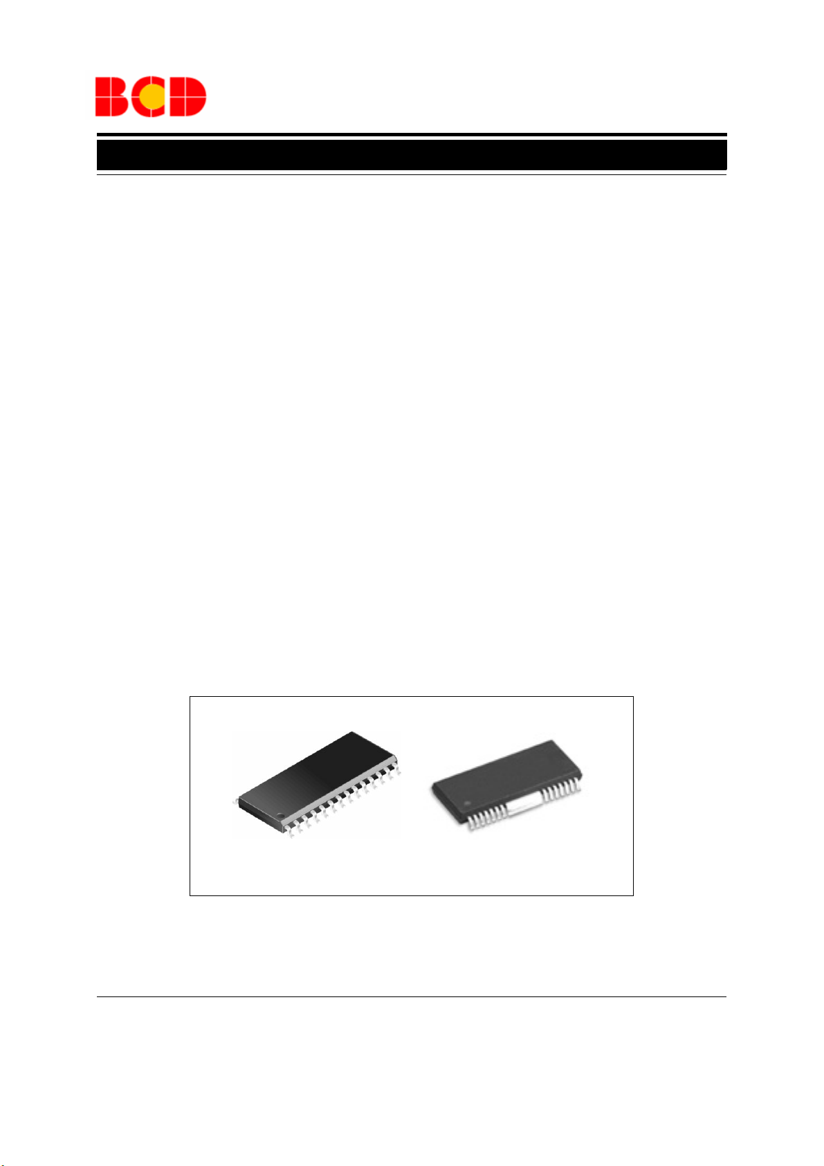
The AP3616 is available in SOIC-28 and HSOP-28
packages.
Features
· Input Voltage Range: 4.2V to 27V
· Maximum Output Current: Typical 1.2A (75mA
per Channel)
· Current Match Accuracy (Typical): ±1.5%
· PWM / Linear Dimming Control
· Open LED Self-check and Protection
· Flexible Short LED Protection
· Under Voltage Lockout Protection
· Over Temperature Protection
· FBX and SYN Pins Enable Parallel Application
· Over Voltage Protection
Applications
· LCD Display Modules
· LCD Monitor
· LCD TV
SOIC-28 HSOP-28
Figure 1. Package Types of AP3616
BCD Semiconductor Manufacturing LimitedJul. 2012 Rev. 1. 2
1
Page 2
Data Sheet
SIXTEEN-CHANNEL, 75mA CURRENT SINK WITH CURRENT MATCH AP3616
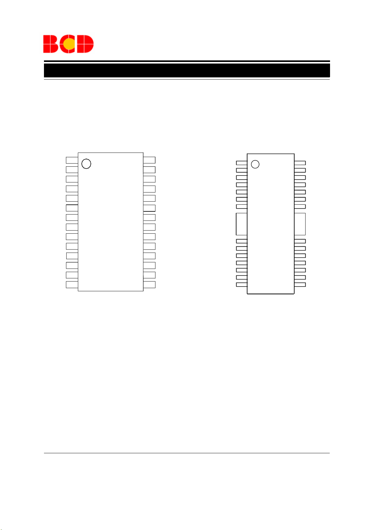
Pin Configuration
CH1
CH2
CH3
CH4
CH5
CH6
CH7
CH8
FLAG
FB
FBX
EN
VIN
GND
10
11
12
13
14
M Package
(SOIC-28)
1
2
3
4
5
6
7
8
9
28
27
26
25
24
23
22
21
20
19
18
17
16
15
CH9
CH10
CH11
CH12
CH13
CH14
CH15
CH16
OVP
SCP
SYN
SYNF
DIM
ISET
CH1
CH2
CH3
CH4
CH5
CH6
CH7
CH8
CH9
CH10
CH11
CH12
CH13
CH14
M28 Package
(HSOP-28)
1
2
3
4
5
6
7
8
9
10
11
12
13
14
28
27
26
25
24
23
22
21
20
19
18
17
16
15
CH16
OVP
SCP
SYN
SYNF
DIM
ISET
GND
VIN
EN
FBX
FB
FLAG
CH15
Figure 2. Pin Configuration of AP3616 (Top View)
BCD Semiconductor Manufacturing LimitedJul. 2012 Rev. 1. 2
2
Page 3

Data Sheet
SIXTEEN-CHANNEL, 75mA CURRENT SINK WITH CURRENT MATCH AP3616
Pin Description
Pin Number
Pin Name Function
SOIC-28 HSOP-28
1 to 8
28 to 21
916FLAG
10 17 FB
11 18 FBX
12 19 EN Enable pin. Logic high enables the IC and logic low disables the IC
13 20 VIN Input voltage pin
14 21 GND Ground pin
15 22 ISET
16 23 DIM
17 24 SYNF
1 to 8
9 to 15 & 28
CH1 to CH8
CH9 to CH16
White LED cathode connection pins. If not used, leave them unconnected
Error flag pin. When LED load goes to error (short or open ), the flag
open drain output will close
Feedback pin. This pin is an interface terminal, which samples the
voltage of each channel, and outputs the lowest voltage of the string
to DC/DC converter
This pin is an interface terminal. Connect it to FB pin can achieve
parallel application. If not used, leave it unconnected
LED current setting pin. An external resistor is connected to this pin.
Current on each channel can be expressed by I
=1.194*1560/R
NEL
Dimming control pin. Adding a PWM signal or DC signal to this pin
to control LED dimming. Connect it to high voltage level if not used
Synchronous PWM frequency setting pin. A nF level of capacitor
should be connected to this pin to set PWM frequency at about 80Hz
to 25kHz
ISET
CHAN-
18 25 SYN
19 26 SCP
20 27 OVP
PWM dimming synchronous pin, this pin outputs DC transformed
PWM signal to synchronize parallel AP3616 and power converter, if
not used, leave it unconnected
LED short trigger voltage setting pin. This pin is used to set the LED
short circuit protection voltage level
This pin is used to trigger OVP condition. OVP triggering voltage
should be lower than the OVP voltage of its cascade chip, such as ,
AP3039A in Figure 19
BCD Semiconductor Manufacturing LimitedJul. 2012 Rev. 1. 2
3
Page 4
Data Sheet
SIXTEEN-CHANNEL, 75mA CURRENT SINK WITH CURRENT MATCH AP3616
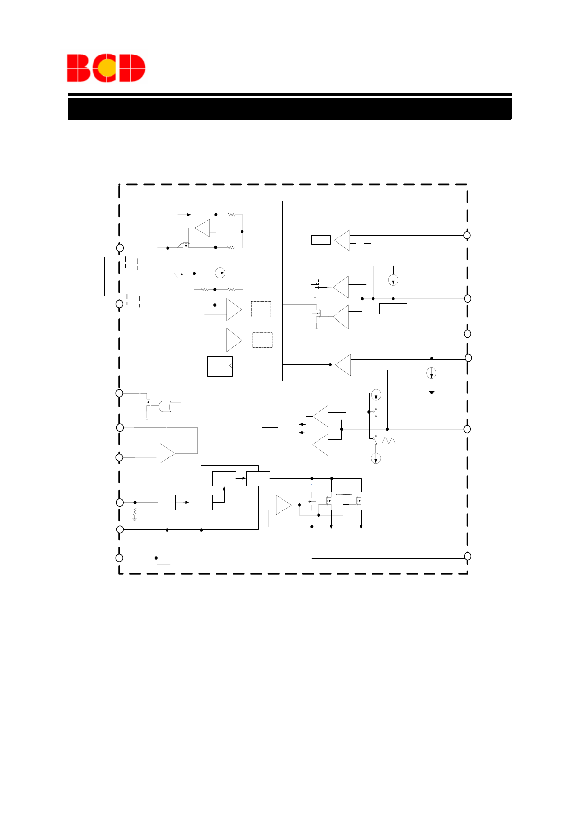
Functional Block Diagram
CH1_I
CH1
CH16
FLAG
FB
FBX
EN
(
1
1
8
8
28
9
21
15
&
28
9(16)
10(17)
11(18)
12(19)
(
VCH 16 to 1
REF
VDD
SCP
200mV
V
DS1=VDD
Open LED
Short LED
LOW
SEL
EN
Bandgap
VDS1
x3120
AMP
x7
PGND
x1
µ
2 A
AGND
x1
AGND
COMP
Short
Detectio n
COMP
Open
Detectio n
OVP_EN
SCP
V
1.194V
REF
COMP
V
=5V
DD
_
VDD
+
COMP
0.26V
V
REF
SCP Open
Detect ion
+
_
COMP
20(27)
OVP
19(26)
SCP
18(25)
SYN
16(23)
Latch
Block
UVLO
PWM
COMP
µ
13 A
+_2.2V
_
SET
RS
Q_BAR
RESET
V
REF
VDD
Regula tor
AMP
COMP
+
0.5V
COMP
µ
13 A
x4
x1
x4
17(24)
DIM
SYNF
13(20)
VIN
14(21)
GND
A(B)
A for SOIC-28
B fro HSOP-28
CH_I
AGND
PGND
Figure 3. Functional Block Diagram of AP3616
4
1 to 16
REF
15(22)
ISET
BCD Semiconductor Manufacturing LimitedJul. 2012 Rev. 1. 2
Page 5
Data Sheet
SIXTEEN-CHANNEL, 75mA CURRENT SINK WITH CURRENT MATCH AP3616
Ordering Information
AP3616 -
Circuit Type
Package
M: SOIC-28
G1: Green
Blank: Tube
M28:HSOP-28
Package Temperature Range Part Number Marking ID Packing Type
SOIC-28
HSOP-28 AP3616M28-G1 AP3616M28-G1
-40 to 85
o
C
AP3616M-G1 AP3616M-G1 Tube
Tube
BCD Semiconductor's Pb-free products, as designated with "G1" suffix in the part number, are RoHS compliant and green.
Absolute Maximum Ratings (Note 1)
Parameter Symbol Value Unit
Input Voltage V
FLAG Pin Voltage V
EN Pin Voltage V
Voltage on Each Channel V
IN
FLAG
EN
CHX
Voltage on Other Seperate Pins -0.3 to 6 V
Thermal Resistance (Junction to
Ambient, No Heat Sink)
Operating Junction Temperature T
Lead Temperature (Soldering, 10sec)
SOIC-28
HSOP-28 59
T
θ
STG
JA
J
ESD (Human Body Model) 2000 V
ESD (Machine Model) 200 V
30 V
30 V
30 V
-0.3 to 60 V
72
o
o
150
-65 to 150
C/W
C/W
o
C
o
C
Note 1: Stresses greater than those listed under "Absolute Maximum Ratings" may cause permanent damage to the device.
These are stress ratings only, and functional operation of the device at these or any other conditions beyond those indicated
under "Recommended Operating Conditions" is not implied. Exposure to "Absolute Maximum Ratings" for extended periods
may affect device reliability.
Jul. 2012 Rev. 1. 2
BCD Semiconductor Manufacturing Limited
5
Page 6

Data Sheet
SIXTEEN-CHANNEL, 75mA CURRENT SINK WITH CURRENT MATCH AP3616
Recommended Operating Conditions
Parameter Symbol Min Max Unit
V
Input Voltage
CC
4.2 27 V
Recommended PWM Dimming Frequency f
Full Scale Setting Current per Channel
=0.5V
V
CHX
V
=0.8V 20 60
CHX
=1.2V 20 75
V
CHX
Operating Temperature Range
PWM
I
CHX
T
A
0.08 25 kHz
20 40
mA
-40 85
o
C
Electrical Characteristics
VIN=24V, VEN=5V, TA=25
ture range (T
=-40
A
Parameter Symbol Conditions Min Typ Max Unit
VCC SECTION
Quiescent Current I
Shutdown Supply Current I
Under Voltage Lockout Threshold V
Under Voltage Lockout Hysteresis V
CHANNEL SECTION
o
C, unless otherwise specified. Boldface type apply over the full operating tempera-
o
C to 85oC).
Q
STBY
UVLO
UVLO_HYS
ISET, SYN and FB
24mA
Pin Floating
VEN=0V, ISET,SYN
0.1 1 µA
and FB Pin Floating
VIN Falling Edge 3.65 3.9 4.15 V
300 mV
Maximum Output Current per Channel I
Current Sink Saturation Voltage per
Channel
Current Matching Accuracy between Any
Two Channels
CHX_MAXVCHX
V
CHX_SATICHX
I
CH_MATCHING
Output Current Load Regulation V
Output Current Line Regulation (Note 2) V
Note 2: Guaranteed by design (GBD).
=0.8V, R
=0 75 mA
ISET
=60mA
I
=60mA,
CHX
=0.8V
V
CH
=0.5V to 2.8V 4 %
CHX
=4.2V to 2.8V 2 %/V
CHX
BCD Semiconductor Manufacturing LimitedJul. 2012 Rev. 1. 2
6
0.6 V
3%
Page 7

Data Sheet
SIXTEEN-CHANNEL, 75mA CURRENT SINK WITH CURRENT MATCH AP3616
Electrical Characteristics (Continued)
VIN=24V, VEN=5V, TA=25
ture range (T
A
=-40
Parameter Symbol Conditions Min Typ Max Unit
DIMMING SECTION
o
C, unless otherwise specified. Boldface type apply over the full operating tempera-
o
C to 85oC).
PWM High Level Threshold Voltage V
PWM Low Level Threshold Voltage V
Linear Dimming Level V
LED SHORT PROTECTION SECTION
SCP Current I
CURRENT SINK SECTION
ISET Reference Voltage V
I
CHX/ISET
Current Multiplication Ratio k R
ENABLE SECTION
EN Pin High Level Threshold V
EN Pin Low Level Threshold V
OVP SECTION
Threshold Voltage V
THRESHOLD
FLAG SECTION
Saturation Voltage V
SYN SECTION
IH_PWM
IL_PWM
L_DIM
SCP
ISET
IH_EN
IL_EN
SAT
2.5 V
0.5 2.2 V
10.5 12.5 14.5 µA
R
=30k, CH1 to
ISET
1.170 1.194 1.218 V
CH16 Floating
ISET
=30k, V
=1V 1615
CHX
2.0 V
1.130 1.194 1.250 V
I
=2mA 0.3 V
SINK
0.3 V
0.8 V
PWM Frequency f
SYNF High Level Output Voltage V
SYNF Low Level Output Voltage V
FB SECTION
Feedback Output Current I
TOTAL DEVICE
Thermal Shutdown Temperature T
Thermal Shutdown Hysteresis T
Jul. 2012 Rev. 1. 2
PWM
OUT_H
OUT_L
FB
OTSD
HYS
0.08 25 kHz
2.4 V
0.4 V
VFB Drop to 97% 13 17 µA
CHX Pin Left Foating 160
20
BCD Semiconductor Manufacturing Limited
7
o
C
o
C
Page 8

Data Sheet
SIXTEEN-CHANNEL, 75mA CURRENT SINK WITH CURRENT MATCH AP3616
Typical Performance Characteristics
VIN=24V, VEN=5V, R
=30kΩ,, TA=25
ISET
o
C, unless otherwise specified.
200
180
160
140
120
100
80
60
40
Maximum Channel Current (mA)
20
0
0.2 0.4 0.6 0.8 1.0 1.2 1.4 1.6
Channel Voltage (V)
Figure 4. Maximum Channel Current vs. Channel Voltage
Figure 5. Feedback Voltage vs. Feedback Current
70
60
50
40
30
20
Current per Channel (mA)
10
0
0.4 0.6 0.8 1.0 1.2 1.4 1.6 1.8 2.0 2.2
Linear Dimming Voltage (V)
0.56
0.54
0.52
0.50
0.48
0.46
0.44
Feedback Voltage (V)
0.42
0.40
4 6 8 10 12 14 16 18 20
Feedback Current (µA)
65
60
55
50
45
40
35
30
25
20
15
10
Current per Channel (mA)
5
0
-5
0 102030405060708090100
f=100Hz
f=20kHz
Duty Cycle (%)
Figure 6. Channel Current vs. Linear Dimming Voltage
Figure 7. Current per Channel vs. Duty Cycle
(PWM Dimming)
BCD Semiconductor Manufacturing LimitedJul. 2012 Rev. 1. 2
8
Page 9

Data Sheet
SIXTEEN-CHANNEL, 75mA CURRENT SINK WITH CURRENT MATCH AP3616
Typical Performance Characteristics (Continued)
VIN=24V, VEN=5V, R
=30kΩ,, TA=25
ISET
o
C, unless otherwise specified.
65
64
63
62
61
60
59
58
Channel Current (mA)
57
56
55
-50 -25 0 25 50 75 100 125 150
Temperature ( oC)
Figure 8. Channel Current vs. Temperature
0.8
0.7
0.6
0.5
0.4
0.3
0.2
Saturation Voltage (V)
0.1
0.0
-50 -25 0 25 50 75 100 125 150
Temperature (oC)
1.4
1.3
1.2
1.1
1.0
0.9
ISET Reference Voltage (V)
0.8
-50 -25 0 25 50 75 100 125 150
Temperature (oC)
Figure 9. ISET Reference Voltage vs. Temperature
2.2
2.1
2.0
1.9
1.8
1.7
1.6
1.5
1.4
1.3
Quiescent Current (mA)
1.2
1.1
1.0
3 6 9 12 15 18 21 24 27
Input Voltage (V)
Figure 10. Saturation Voltage vs. Temperature Figure 11. Quiescent Current vs. Input Voltage
Jul. 2012 Rev. 1. 2
BCD Semiconductor Manufacturing Limited
9
Page 10

Data Sheet
SIXTEEN-CHANNEL, 75mA CURRENT SINK WITH CURRENT MATCH AP3616
Typical Performance Characteristics (Continued)
VIN=24V, VEN=5V, R
=30kΩ,, TA=25
ISET
o
C, unless otherwise specified.
63.6
63.4
63.2
63.0
62.8
62.6
62.4
62.2
62.0
61.8
61.6
61.4
61.2
61.0
60.8
Current per Channel (mA)
60.6
60.4
60.2
60.0
0 2 4 6 8 10 12 14 16
Channel
TA=-40oC
TA=125oC
TA=25oC
V
5V/div
V
SYN
5V/div
V
GATE
10V/div
I
50mA/div
DIM
CH
Time 4ms/div
Figure 12. Current per Channel vs. Channel Figure 13. PWM Dimming (f=100Hz, Duty Cycle=50%)
V
SYNF
V
5V/div
V
SYN
5V/div
V
GATE
10V/div
I
CH
50mA/div
DIM
Time 20µs/div
1V/div
V
SYN
5V/div
V
GATE
10V/div
I
CH
100mA/div
Time 80 0µs/div
Figure 14. PWM Dimming (f=20kHz, Duty Cycle=50%) Figure 15. Linear Dimming (V
BCD Semiconductor Manufacturing LimitedJul. 2012 Rev. 1. 2
10
DIM
=1.4V)
Page 11

Data Sheet
SIXTEEN-CHANNEL, 75mA CURRENT SINK WITH CURRENT MATCH AP3616
Typical Performance Characteristics (Continued)
VIN=24V, VEN=5V, R
=30kΩ,, TA=25
ISET
o
C, unless otherwise specified.
V
OVP
1V/div
I
50mA/div
V
1V/div
V
FLAG
5V/div
CH
FB
Time 400 µs/div
V
SCP
1V/div
I
100mA/div
V
5V/div
V
FLAG
5V/div
CH
CH
Time 4µs/div
Figure 16. LED Open Protection Figure 17. LED Short Protection
V
GATE
5V/div
I
CH
50mA/div
Time 2s/div
Figure 18. OTP and Recovery
Jul. 2012 Rev. 1. 2
11
BCD Semiconductor Manufacturing Limited
Page 12

Data Sheet
+
SIXTEEN-CHANNEL, 75mA CURRENT SINK WITH CURRENT MATCH AP3616
Function Description
1. LED Current Setting
The maximum LED current per channel can be
adjusted up to 75mA via ISET pin. When ≥ 75mA
current is needed in application, two or more channels
can be paralleled to provide larger drive current. Connect a resistor R
set the reference current I
determined by the following equation.
)(
=
mAI
LED
2. Dimming Control
The AP3616 provides two dimming methods: external
PWM signal or DC voltage input. Applying a PWM
signal to DIM pin to adjust the LED current, that
means, the LED current of all enabled channels can be
adjusted at the same time and the LED brightness can
be adjusted from 1%*I
During the high level period of PWM signal, the LED
is turned on and 100% of the current flows through
LED, while during the low level period of the PWM
signal, the LED is turned off and almost no current
flows through the LED, thus changing the average
current through LED and finally adjusting LED
brightness. The external PWM signal frequency
applied to PWM pin is allowed to be 80Hz or higher.
3.Over Voltage Protection
between ISET pin and GND to
ISET
. The LED current is
SET
⋅
Vk
ISET
Ω
CHX_MAX
=
)(
to 100%*I
194.10156
×
Ω
kRkR
ISETISET
)(
CHX_MAX
The AP3616 integrates an OVP circuit. The OVP pin
is connected to the center tap of voltage-divider (R
and R
and GND (Figure 19). If the voltage on OVP pin
exceeds 1.194V, which may results from open loop or
excessive output voltage, the AP3616 will start LED
open protection.
4. LED Short-circuit Protection
The AP3616 integrates an LED short-circuit
protection circuit. During normal operation, any shortcircuited LED will cause the corresponding LED pin
voltage to rise. If any LED pin voltage exceeds 8
times of the voltage at SCP pin, the corresponding
LED current sink will be latched off, while the
remaining string(s) keep normal operation. Toggle the
VIN and/or EN to reset the latch. An internal current
.
source was connected to this pin, a resistor connected
here is used to set the shorting LED trigger voltage.
5. LED Open-circuit Protection
The AP3616 integrates an LED Open-Circuit Protection circuit. When any LED string is open, V
boost up until the voltage at OVP pin reaches an
approximate 1.194V threshold. The IC will automatically ignore the open string(s) whose CHX pin voltage
is less than 100mV.
) that placed between high voltage output
OV4
×
V
OVP
=
R
OV4OV3
OV4
V194.1)R(R
OUT
OV3
will
BCD Semiconductor Manufacturing LimitedJul. 2012 Rev. 1. 2
12
Page 13

Data Sheet
SIXTEEN-CHANNEL, 75mA CURRENT SINK WITH CURRENT MATCH AP3616
Typical Application
R2
C1
(Optional)
(Optional)
+24V
C
µ
22 F/50V
IN1
+24V (VCC)
L
µ
C
C
IN2
IN3
UVLO_1
20k
R
1
UVLO
OVP1
2
R1
EN
Ω
51
2.7k
UVLO_2
R
OV
3
EN
4
VIN
5
VCC
6
OUT
V
78
C
µ
GND
0.47 F/25V
47 H/4A
C
ss
100k
22nF/16V
C
C
R
C
3.9k
10nF/16V
R10
R
T
(Optional)
C4
R
G
Ω
2
14
SS
13
COMP
12
FB
11
SHDN
10
GND
AP3039A
9
CS
RT
U1
Single Chip Application (12S16P)
R3
(Optional)
MBRD360
60V/3A
FQD13N06L
60V/11A
D
10 F/100V
V
OUT
R
R
OV1
200k 150k
OVP1 OVP2
OV2
OV3
R
OV4
4.3k
C
C
OUT1
µ
OUT2
µ
10 F/100V
R
4.3k
LED Arrays
12x16
R10
PWM
SYN
CH1
R6
30k
CH2
AP3616
FB
VIN
ISET
GND
SCP
C3
R7
6.8nF
130k
µ
R
R
(Optional)
300m
CS2
CS1
300m
Ω
Ω
R4
100k
R5 62k
V
=24V
CC
C2
µ
0.1 F/50V
CH16
DIM
FBX
OVP
EN
FLAG
SYNF
R8
Ω
51
R9
1k
OVP2
EN
+5V
PWM / Linear
Dimming
Ω
51
µ
1 F
(Optional)
+24V
C
µ
22 F/50V
IN1
+24V (VCC)
R2
C1
(Optional)
(Optional)
R11_1
(Optional)
C4
(Optional)
R3
MBRD360
60V/3A
FQD13N06L
60V/11A
R
R
CS2
CS1
(Optional)
300m
300m
Ω
R4
100k
D
C
µ
10 F/100V
Ω
V
CC
OUT1
R5 62k
=24V
C2
µ
0.1 F/50V
V
OUT
C
OUT2
µ
10 F/100V
R
OV2
4.3k
R
OV1
200k
OVP1 OVP2
SYN
FB
U2
VIN
R6_1
30k
R
150k
ISET
OV3
R
OV4
4.3k
CH1
AP3616
GND
R7_1
130k
SCP
6.8nF
C3_1
CH2
SYNF
R8_1
Ω
51
EN
L
µ
C
C
IN2
IN3
UVLO_1
20k
R
1
UVLO
OVP1
2
R1
EN
Ω
51
OV
3
EN
4
VIN
5
VCC
2.7k
6
OUT
V
78
UVLO_2
C
µ
GND
R
0.47 F/25V
47 H/4A
C
ss
22nF/16V
14
SS
C
C
R
C
13
COMP
3.9k
10nF/16V
12
FB
11
SHDN
10
GND
AP3039A
9
CS
R
T
RT
100k
U1
R
G
2Ω
EN
R9_1
LED Arrays
12x32
PWM
SYN
CH1
CH16
DIM
FBX
VCC=24V
OVP
FLAG
C2
µ
0.1 F/50V
OVP2
1k
+5V
CH2
AP3616
FB
U3
VIN
ISET
GND
SCP
SYNF
C3
R7
R6
6.8nF
130k
30k
R10
OVP2
PWM / Linear
Dimming
Ω
51
µ
1 F
(Optional)
CH16
DIM
FBX
OVP
EN
FLAG
R8
R9
Ω
51
1k
+5V
Multi Chips Application (12S32P)
Figure 19. Typical Applications of AP3616
Jul. 2012 Rev. 1. 2
BCD Semiconductor Manufacturing Limited
13
Page 14

Data Sheet
SIXTEEN-CHANNEL, 75mA CURRENT SINK WITH CURRENT MATCH AP3616
Mechanical Dimensions
SOIC-28
17.700(0.697)
18.100(0.713)
10.210(0.402)
10.610(0.418)
1.270(0.050)
BSC
7.400(0.291)
0.400(0.016)
1.270(0.050)
Unit: mm(inch)
0.204(0.008)
0.330(0.013)
°
0
°
8
7.700(0.303)
0.330(0.013)
0.510(0.020)
2.290(0.090)
2.500(0.098)
Note: Eject hole, oriented hole and mold mark is optional.
0.100(0.004)
0.300(0.012)
2.350(0.093)
2.650(0.104)
BCD Semiconductor Manufacturing LimitedJul. 2012 Rev. 1. 2
14
Page 15

Data Sheet
SIXTEEN-CHANNEL, 75mA CURRENT SINK WITH CURRENT MATCH AP3616
Mechanical Dimensions (Continued)
10.000(0.394)
10.650(0.419)
7.400(0.291)
7.600(0.300)
0.230(0.009)
0.470(0.019)
HSOP-28
17.890(0.704)
18.190(0.716)
5.050(0.199)
5.250(0.207)
0.800(0.031)
0.100(0.004)
0.300(0.012)
0.400(0.016)
1.270(0.050)
TYP
Unit: mm(inch)
0.204(0.008)
0.360(0.014)
o
o
8
0
~
2.180(0.086)
2.330(0.092)
Note: Eject hole, oriented hole and mold mark is optional.
2.280(0.090)
2.630(0.104)
BCD Semiconductor Manufacturing LimitedJul. 2012 Rev. 1. 2
15
Page 16

BCD Semiconductor Manufacturing Limited
IMPORTANT NOTICE
IMPORTANT NOTICE
BCD Semiconductor Manufacturing Limited reserves the right to make changes without further notice to any products or specifi-
BCD Semiconductor Manufacturing Limited reserves the right to make changes without further notice to any products or specifi-
cations herein. BCD Semiconductor Manufacturing Limited does not assume any responsibility for use of any its products for any
cations herein. BCD Semiconductor Manufacturing Limited does not assume any responsibility for use of any its products for any
particular purpose, nor does BCD Semiconductor Manufacturing Limited assume any liability arising out of the application or use
particular purpose, nor does BCD Semiconductor Manufacturing Limited assume any liability arising out of the application or use
of any its products or circuits. BCD Semiconductor Manufacturing Limited does not convey any license under its patent rights or
of any its products or circuits. BCD Semiconductor Manufacturing Limited does not convey any license under its patent rights or
other rights nor the rights of others.
other rights nor the rights of others.
http://www.bcdsemi.com
MAIN SITE
MAIN SITE
- Headquarters
BCD Semiconductor Manufacturing Limited
BCD Semiconductor Manufactur ing Limited
- Wafer Fab
No. 1600, Zi Xing Road, Shanghai ZiZhu Science-based Industrial Park, 200241, China
Shanghai SIM-BCD Semiconductor Manufacturing Limited
Tel: +86-21-24162266, Fax: +86-21-24162277
800, Yi Shan Road, Shanghai 200233, China
Tel: +86-21-6485 1491, Fax: +86-21-5450 0008
REGIONAL SALES OFFICE
Shenzhen Office
REGIONAL SALES OFFICE
Shanghai SIM-BCD Semiconductor Manufacturing Co., Ltd., Shenzhen Office
Shenzhen Office
Unit A Room 1203, Skyworth Bldg., Gaoxin Ave.1.S., Nanshan District, Shenzhen,
Shanghai SIM-BCD Semiconductor Manufacturing Co., Ltd. Shenzhen Office
China
Advanced Analog Circuits (Shanghai) Corporation Shenzhen Office
Tel: +86-755-8826 7951
Room E, 5F, Noble Center, No.1006, 3rd Fuzhong Road, Futian District, Shenzhen 518026, China
Fax: +86-755-8826 7865
Tel: +86-755-8826 7951
Fax: +86-755-8826 7865
- Wafer Fab
BCD Semiconductor Manufacturing Limited
Shanghai SIM-BCD Semiconductor Manufacturing Co., Ltd.
- IC Design Group
800 Yi Shan Road, Shanghai 200233, China
Advanced Analog Circuits (Shanghai) Corporation
Tel: +86-21-6485 1491, Fax: +86-21-5450 0008
8F, Zone B, 900, Yi Shan Road, Shanghai 200233, China
Tel: +86-21-6495 9539, Fax: +86-21-6485 9673
Taiwan Office
BCD Semiconductor (Taiwan) Company Limited
Taiwan Office
4F, 298-1, Rui Guang Road, Nei-Hu District, Taipei,
BCD Semiconductor (Taiwan) Company Limited
Tai wan
4F, 298-1, Rui Guang Road, Nei-Hu District, Taipei,
Tel: +886-2-2656 2808
Taiwan
Fax: +886-2-2656 2806
Tel: +886-2-2656 2808
Fax: +886-2-2656 2806
USA Office
BCD Semiconductor Corp.
USA Office
30920 Huntwood Ave. Hayward,
BCD Semiconductor Corporation
CA 94544, USA
30920 Huntwood Ave. Hayward,
Tel : +1-510-324-2988
CA 94544, U.S.A
Fax: +1-510-324-2788
Tel : +1-510-324-2988
Fax: +1-510-324-2788
 Loading...