Data Sheet
100mA REGULATED CHARGE PUMP AP3602A/B
General Description
The AP3602A/B are regulated step-up DC/DC
converters based on charge pump technique. These ICs
have the ability to supply 100mA constant output
current or 250mA peak output current for 100ms from
3.0V to 5V input (2.7V to 4.5 V for AP3602B), so they
can be used as white LEDs driver or flash LED driver.
The AP3602A/B have very low power dissipation and
high efficiency in typical applications. Other features
include over-temperature protection, low temperature
coefficient and etc. to meet some special requirements
of hand-held battery powered devices.
Only 3 external capacitors are required in applications,
which helps to save space and lower cost. These chips
also have a disable terminal to turn on or turn off the
chip to ease the use.
The AP3602A/B are available in SOT-23-6 package.
Features
· Low Quiescent Current: 13μA Typical
· Regulated Output Voltage Precision: 4%
· High Output Current:
100mA when V
50mA when V
· High Frequency: up to 1.2 MHz
· Low Shutdown Supply Current: <1
· High Output Peak Current: 250mA for 100ms
· Over Temperature Protection
· Operating Temperature Range: -40
IN
≥2.7V
IN
≥3.0V
μA
o
C to 85oC
Applications
· Mobile Phone Backlight Driver
· Camera Flash LED Driver
· MP3, MP4
· Handheld Device
· Portable Communication Device
SOT-23-6
Figure 1. Package Type of AP3602A/B
Dec. 2012 Rev. 2. 0 BCD Semiconductor Manufacturing Limited
1

Data Sheet
1
2
34
5
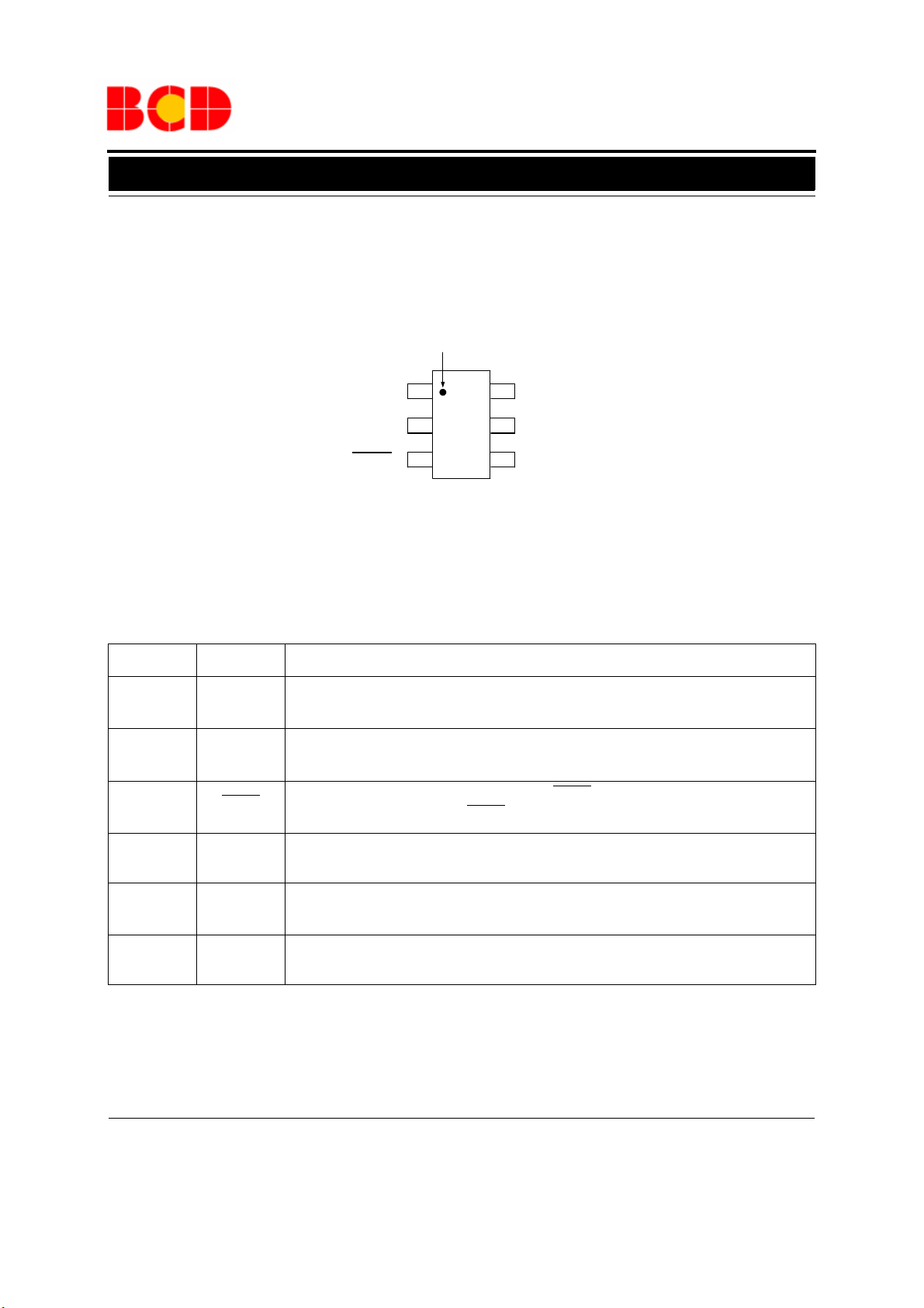
Pin 1 Mark
6
100mA REGULATED CHARGE PUMP AP3602A/B
Pin Configuration
K Package
(SOT-23-6)
V
OUT
GND
SHDN
C+
V
C-
IN
Figure 2. Pin Configuration of AP3602A/B (Top View)
Pin Description
Pin Number Pin Name Function
1
V
OUT
2 GND
3 SHDN
Regulated Output Voltage. V
capacitor which is placed as close to the pin as possible for best performance
Ground. GND should be tied to a ground plane for best performance. The C
should be placed as close to this pin as possible
Active Low Shutdown Input. A low signal on SHDN disables the AP3602A/B, while a high
signal enables the AP3602A/B. SHDN
should be bypassed with a 1μF to 22μF low ESR ceramic
OUT
pin must not be allowed to float
OUT
and C
IN
4C-
5
6C+
Dec. 2012 Rev. 2. 0 BCD Semiconductor Manufacturing Limited
Flying Capacitor Negative Terminal. The flying capacitor should be placed as close to this pin
as possible
IN
which is placed as close to the pin as possible for best performance
Input Supply Voltage. V
V
should be bypassed with a 1μF to 22μF low ESR ceramic capacitor
IN
Flying Capacitor Positive Terminal. The flying capacitor should be placed as close to this pin
as possible
2

Data Sheet
3
5
4
2
1
1.25V
OSC
6
S3
S4
S1
S2
COMP
EN
R1
R2
CONTROL
+
-
OTP
100mA REGULATED CHARGE PUMP AP3602A/B
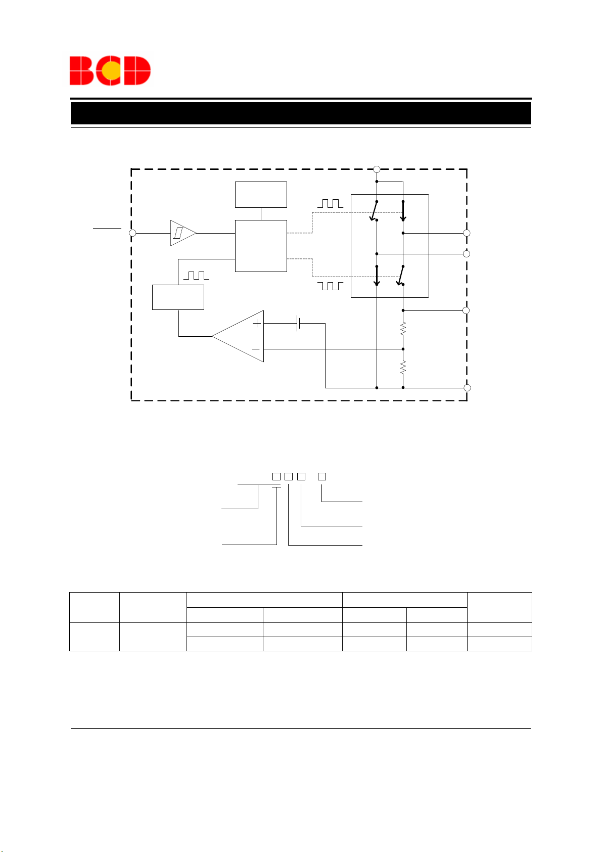
Functional Block Diagram
V
IN
SHDN
Ordering Information
Circuit Type
Output Voltage
A: 5V
B: 4.5V
Figure 3. Functional Block Diagram of AP3602A/B
AP3602
-
E1: RoHS
G1: Green
TR: Tape and Reel
Package
K: SOT-23-6
C+
C-
V
OUT
GND
Package
SOT-23-6
BCD Semiconductor's products as designated with "E1" suffix in the part number are RoHS compliant. Products with "G1" suffix are available in green packages.
Temperature
Range
-40 to 85
AP3602AKTR-E1 AP3602AKTR-G1 E7T G7T Tape & Reel
o
C
AP3602BKTR-E1 AP3602BKTR-G1 E8T G8T Tape & Reel
Part Number Marking ID
RoHS Green RoHS Green
Packing Type
Dec. 2012 Rev. 2. 0 BCD Semiconductor Manufacturing Limited
3

Data Sheet
100mA REGULATED CHARGE PUMP AP3602A/B
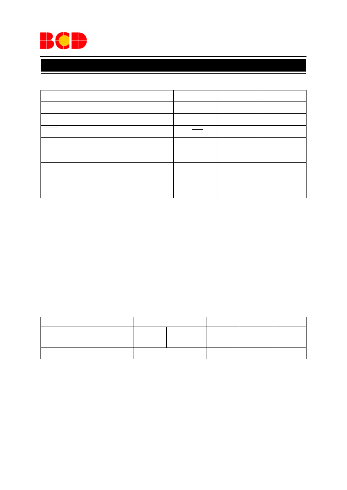
Absolute Maximum Ratings (Note 1)
Parameter Symbol Value Unit
Input Voltage V
Output Voltage V
SHDN
Pin Voltage V
Thermal Resistance (Junction to Ambient, no Heat sink) R
Operating Junction Temperature T
Storage Temperature Range T
Lead Temperature (Soldering, 10sec) T
IN
O
SHDN
θJA
J
STG
LEAD
7V
7V
7V
300
150
-65 to 150
260
o
C/W
o
o
o
C
C
C
ESD (Human Body Model) 2000 V
Note 1: Stresses greater than those listed under "Absolute Maximum Ratings" may cause permanent damage to
the device. These are stress ratings only, and functional operation of the device at these or any other conditions
beyond those indicated under "Recommended Operating Conditions" is not implied. Exposure to "Absolute Maximum Ratings" for extended periods may affect device reliability.
Recommended Operating Conditions
Parameter Symbol Min Max Unit
Input Voltage
V
IN
Operating Temperature T
Dec. 2012 Rev. 2. 0 BCD Semiconductor Manufacturing Limited
AP3602A 2.7 5
AP3602B 2.7 4.5
A
-40 85
4
V
o
C

Data Sheet
100mA REGULATED CHARGE PUMP AP3602A/B
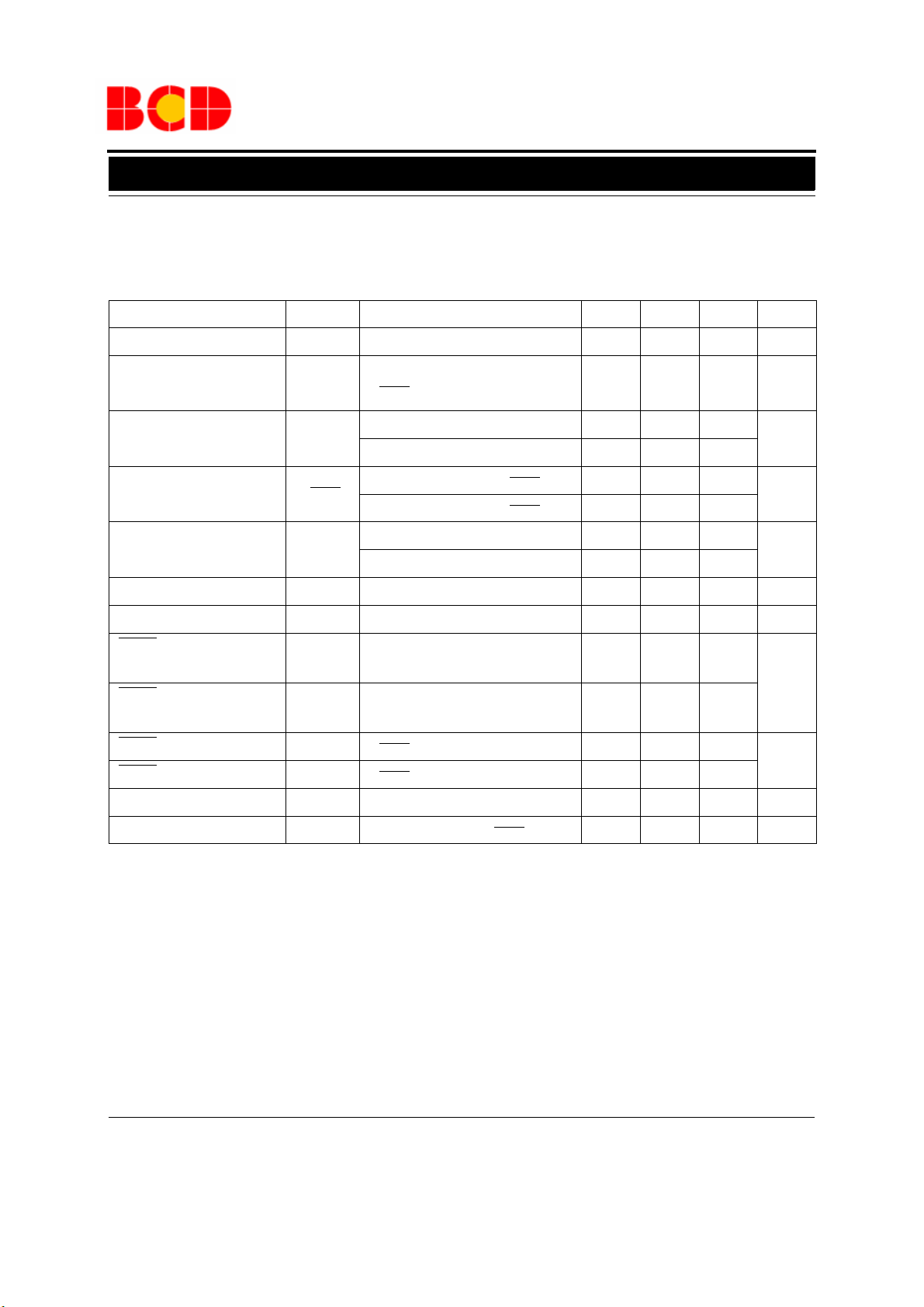
Electrical Characteristics
(C
FLY
=1μF, CIN=C
=10μF, TA=25
OUT
o
C, unless otherwise specified.)
For AP3602A
Parameter Symbol Conditions Min Typ Max Unit
Input Voltage V
Quiescent Current
Output Voltage
Shutdown Supply Current
Ripple Voltage
I
V
RIPPLE
Efficiency
Frequency f
SHDN
Input Threshold
High
SHDN
Input Threshold
Low
Input Current High I
SHDN
Input Current Low I
SHDN
V
Turn-on Time t
OUT
Short-Circuit Current I
IN
I
Q
V
O
SHDN
η
OSC
V
IH
V
IL
IH
IL
ON
SC
VO=5V 2.7 V
VIN=2.7V to 5.0V, IO=0mA,
=VIN, Not Switching
V
SHDN
2.7V<VIN<5V, I
3.0V<V
IN
2.7V<VIN<3.6V, IO=0, V
3.6V<V
IN
≤50mA
O
<5V, I
≤100mA
O
<5.0V, IO=0, V
SHDN
SHDN
4.8 5.0 5.2
4.8 5.0 5.2
=0V 0.01 1
=0V 2.5
13 30 μA
VIN=2.7V, IO=50mA 25
O
V
V
μA
mV
VIN=3V, IO=100mA 30
VIN=2.7V, IO=50mA 92 %
Oscillator free running 1.2 MHz
1.4
V
0.3
V
=V
V
SHDN
SHDN
IN
=GND -1 1
VIN=3V, IO=0mA 0.2
VIN=3V, VO=GND, V
=3V 300 mA
SHDN
-1 1
μA
ms
PP
Dec. 2012 Rev. 2. 0 BCD Semiconductor Manufacturing Limited
5

Data Sheet
100mA REGULATED CHARGE PUMP AP3602A/B
Electrical Characteristics (Continued)
(C
FLY
=1μF, CIN=C
=10μF, TA=25
OUT
o
C, unless otherwise specified.)
For AP3602B
Parameter Symbol Conditions Min Typ Max Unit
Input Voltage V
Quiescent Current
Output Voltage
Shutdown Supply Current
Ripple Voltage
I
V
RIPPLE
Efficiency
Frequency f
SHDN
Input Threshold
High
SHDN
Input Threshold
Low
Input Current High I
SHDN
Input Current Low I
SHDN
V
Turn-on Time t
OUT
Short-Circuit Current I
IN
I
Q
V
O
SHDN
η
OSC
V
IH
V
IL
IH
IL
ON
SC
VO=4.5V 2.7 V
VIN=2.7V to 4.5V, IO=0mA,
=VIN, Not Switching
V
SHDN
13 30 μA
2.7V<VIN<4.5V, IO<50mA 4.32 4.5 4.68
3.0V<V
2.7V<VIN<3.6V, IO=0, V
3.6V<V
<4.5V, IO<100mA 4.32 4.5 4.68
IN
=0V 0.01 1
SHDN
<4.5V, IO=0, V
IN
=0V 2.5
SHDN
VIN=2.7V, IO=50mA 25
O
V
V
μA
mV
VIN=3V, IO=100mA 30
VIN=2.7V, IO=50mA 83 %
Oscillator free running 1.2 MHz
1.4
V
0.3
V
=V
V
SHDN
SHDN
IN
=0V -1 1
VIN=3V, IO=0mA 0.2
VIN=3V, VO=GND, V
=3V 300 mA
SHDN
-1 1
μA
ms
PP
Dec. 2012 Rev. 2. 0 BCD Semiconductor Manufacturing Limited
6
 Loading...