Diodes AP3586A, AP3586B, AP3586C User Manual

Single Phase Synchronous Buck PWM Controller AP3586A/B/C
Data sheet
General Description
The AP3586A/B/C is a compact synchronous
-rectified buck controller specifically designed to
operate from 5V or 12V supply voltage and deliver
high-quality output voltage as low as 0.6V
(AP3586A) or 0.8V (AP3586B/C). This device
operates at fixed 300kHz (AP3586A/B) or 200kHz
(AP3586C) frequency and provides an optimal level
of integration to reduce size and cost of the power
supply.
This controller integrates internal MOSFET drivers
that support 12V+12V bootstrapped voltage for highefficiency power conversion. The bootstrap diode is
built-in to simplify the circuit design and minimize
external part count.
This controller provides single feedback loop,
voltage-mode control with fast transient response.
The error amplifier features a 10MHz gain-bandwidth
product and 6V/µs slew rate which enables high
converter bandwidth for fast transient performance.
Other features include internal soft-start, under
voltage protection, over current protection and
shutdown function. With afore-mentioned functions,
this part provides customers a compact, high
efficiency, well-protected and cost-effective
solutions.
The AP3586A/B/C is available in SOIC-8 and
PSOP-8 packages.
Figure 1. Package Types of AP3586A/B/C
SOIC-8/PSOP-8
Features
• Supply Voltage: 5V/12V
• V
• 0.6V/0.8V to 82% of V
• Internal Reference: 0.6V/0.8V
• Simple Single-loop Control
• Voltage-mode PWM Control
• Duty Cycle: 0% to 82%
• Fast Transient Response
• 10MHz High-bandwidth Error Amplifier with
• Fixed Oscillator Frequency: 300kHz/200kHz
• Lossless, Programmable Over Current Protection
• Start-up into Pre-biased Load
• Built-in Thermal Shutdown
• Built-in Soft-start
• Over Current Protection
• Over Voltage Protection
• Under Voltage Protection
• Integrated Boot Diode
Input Range: 3.3V to 12V
IN
IN
6V/µs Slew Rate
(Uses Lower MOSFET R
Output Range
)
DS(ON)
Applications
• Subsystem Power Supplies
• PCI, AGP, Graphics Cards, Digital TV
• SSTL-2 and DDR/2/3 SDRAM Bus Termination
Supply
• Cable Modems, Set Top Boxes, and DSL
Modems
• Industrial Power Supplies and General Purpose
Supplies
Mar. 2012 Rev. 1. 1 BCD Semiconductor Manufacturing Limited
1

Data sheet
Single Phase Synchronous Buck PWM Controller AP3586A/B/C
Pin Configuration
M Package
(SOIC-8)
MP Package
(PSOP-8)
1
2
3
4
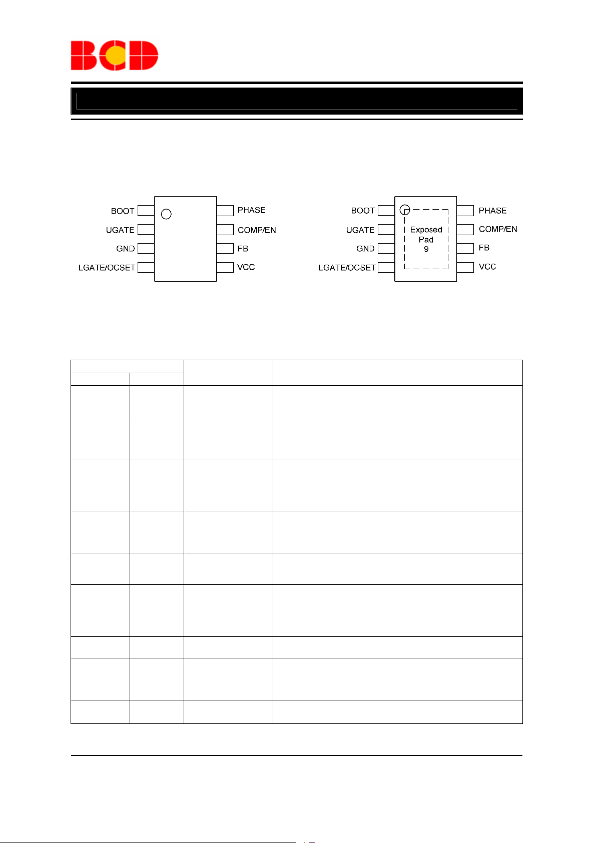
Figure 2. Pin Configuration of AP3586A/B/C (Top View)
8
7
6
5
Pin Description
Pin Number
SOIC-8 PSOP-8
1 1 BOOT
2 2 UGATE
3 3 GND
4 4 LGATE/OCSET
5 5 VCC
6 6 FB
7 7 COMP/EN
8 8 PHASE
9 Exposed Pad
Pin Name Function
1
2
3
4
8
7
6
5
Bootstrap pin. Connect a bootstrap capacitor from this pin to
PHASE for creating a BOOT voltage suitable to drive a standard
N-Channel MOSFET.
Upper-gate drive pin. Connect this pin to the upper MOSFET gate
providing the gate drive. This pin is monitored by the adaptive
shoot-through protection circuitry to determine when the upper
MOSFET has turned off.
Ground for the IC. All voltage levels are measured with respect to
this pin. Connect this pin directly to the low side MOSFET source
and ground plane with the lowest impedance. The exposed pad
must be soldered to a large PCB and connected to GND for
maximum power dissipation.
Low-side Gate Driver Output and Over-Current Setting Input.
This pin is the gate driver for low-side MOSFET. It is also used to
set the maximum inductor current. Refer to the section in
“Function Description” for detail.
Bias supply pin. Provides a 5V or 12V bias supply for the chip
from this pin. The pin should be bypassed with a capacitor to
GND.
Feedback pin. This pin is the inverting input of the internal error
amplifier. Use FB pin, in combination with the COMP pin, to
compensate the voltage control feedback loop of the converter. A
resistor divider from output to GND is used to set the output
voltage.
Compensation and disable pin. This pin is the output of the Error
Amplifier. Pull COMP pin low will shut down the IC.
This pin connects to the source of the upper MOSFET and the
drain of the lower MOSFET. This pin is also monitored by the
adaptive shoot-through protection circuitry to determine when the
upper MOSFET has turned off.
Exposed Pad as ground pin.
Mar. 2012 Rev. 1. 1 BCD Semiconductor Manufacturing Limited
2

Data sheet
Single Phase Synchronous Buck PWM Controller AP3586A/B/C
Functional Block Diagram
5
1
2
8
4
/0.6V
6
7
/EN
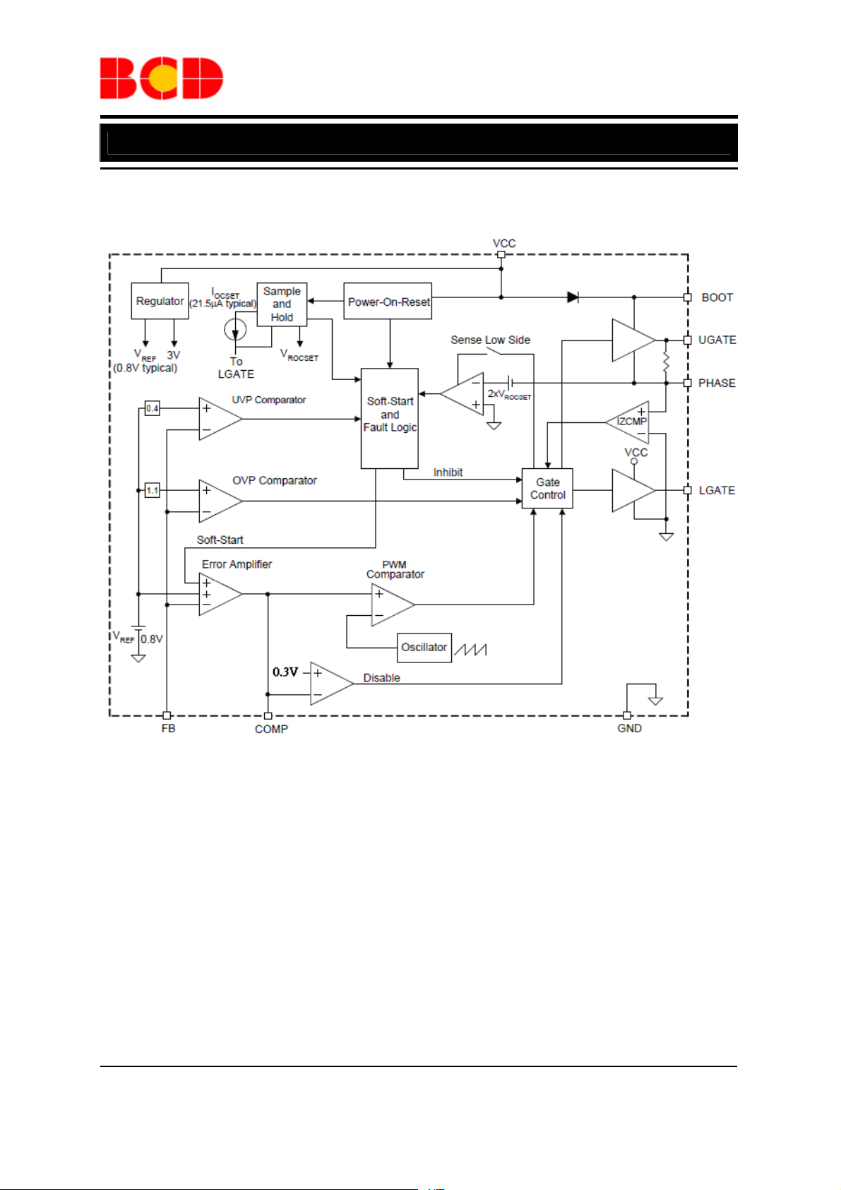
Figure 3. Functional Block Diagram of AP3586A/B/C
3
/OCSET
Mar. 2012 Rev. 1. 1 BCD Semiconductor Manufacturing Limited
3

Data sheet
Single Phase Synchronous Buck PWM Controller AP3586A/B/C
Ordering Information
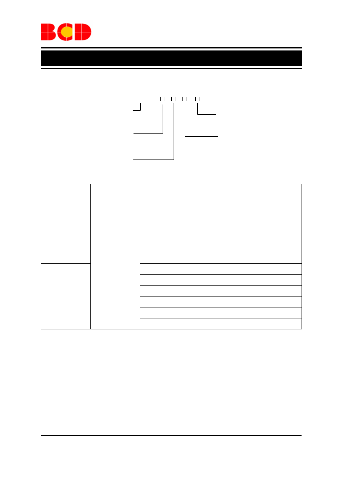
AP3586 -
G1: Green
Blank: Tube
TR: Tape & Reel
Package
Circuit Type
A: AP3586A
B: AP3586B
C: AP3586C
Package
M: SOIC-8
MP: PSOP-8
Temperature
Range
Part Number Marking ID Packing Type
AP3586AM-G1 3586AM-G1 Tube
AP3586AMTR-G1 3586AM-G1 Tape & Reel
SOIC-8
-40 to 85°C
PSOP-8
AP3586BM-G1 3586BM-G1 Tube
AP3586BMTR-G1 3586BM-G1 Tape & Reel
AP3586CM-G1 3586CM-G1 Tube
AP3586CMTR-G1 3586CM-G1 Tape & Reel
AP3586AMP-G1 3586AMP-G1 Tube
AP3586AMPTR-G1 3586AMP-G1 Tape & Reel
AP3586BMP-G1 3586BMP-G1 Tube
AP3586BMPTR-G1 3586BMP-G1 Tape & Reel
AP3586CMP-G1 3586CMP-G1 Tube
AP3586CMPTR-G1 3586CMP-G1 Tape & Reel
BCD Semiconductor's Pb-free products, as designated with "G1" suffix in the part number, are RoHS compliant
and green.
Mar. 2012 Rev. 1. 1 BCD Semiconductor Manufacturing Limited
4

Data sheet
Single Phase Synchronous Buck PWM Controller AP3586A/B/C
Absolute Maximum Ratings (Note 1)
Parameter Symbol Value Unit
Supply Input Voltage
BOOT Voltage
UGATE to PHASE Voltage V
PHASE, LGATE to GND Voltage
Other Pin Voltage -0.3 to 6 V
Power Dissipation PD TBD mW
Thermal Resistance
Operating Junction Temperature TJ -40 to 125 ºC
Storage Temperature T
Lead Temperature (Soldering, 10 sec) T
ESD (Human Body Model) (Note 2) 2000 V
ESD (Machine Model) (Note 2) 200 V
VCC
V
BOOT
-0.3 to 15 V
UGATE
,
V
PHASE
V
LGATE
θ
JA
-65 to 150 ºC
STG
260 ºC
LEAD
-0.3 to 15 V
-0.3 to V
-1 to 15 V
+15 V
PHASE
50 ºC/W
Note 1: Stresses greater than those listed under “Absolute Maximum Ratings” may cause permanent damage to
the device. These are stress ratings only, and functional operation of the device at these or any other conditions
beyond those indicated under “Recommended Operating Conditions” is not implied. Exposure to “Absolute
Maximum Ratings” for extended periods may affect device reliability.
Note 2: Devices are ESD sensitive. Handling precaution is recommended.
Recommended Operating Conditions
Parameter Symbol Min Max Unit
Supply Input Voltage VCC 5 12 V
Operating Ambient Temperature TA -40 85
°C
Mar. 2012 Rev. 1. 1 BCD Semiconductor Manufacturing Limited
5

Data sheet
Single Phase Synchronous Buck PWM Controller AP3586A/B/C
Electrical Characteristics
VCC=12V, TA=25°C, unless otherwise specified.
Parameter Symbol Conditions Min Typ Max Unit
SUPPLY INPUT
Supply Current
Quiescent Supply Current
ICC
I
CC_Q
Power Input Voltage VIN 3.0 13.2 V
POWER ON RESET
VCC Rising Threshold V
VCC Threshold Hysteresis V
POR
POR_HYS
UGATE and LGATE Pins
Open; Switching
V
No Switching
FB=VREF
+0.1V,
VCC Rising
5 mA
4 mA
4.0 4.2 4.4 V
500 mV
OSCILLA TOR
Oscillator Frequency
f
OSC
For AP3586A/B 270 300 330 kHz
For AP3586C 180 200 220 kHz
∆V
Ramp Amplitude
OSC
1.4 V
P-P
ERROR AMPLIFIER
G
Open Loop DC Gain
Gain-bandwidth Product
Slew Rate SR 3 6
Transconductance 800 1100
Output Source Current
Output Sink Current
DC_OL
GBW
55 70 dB
10 MHz
V/µs
µA/V
FB<VREF
FB>VREF
80 120
80 120
µA
µA
V
V
PWM CONTROLLER GATE DRIVERS
Upper Gate Source
Current
Upper Gate Sink Current I
Upper Gate Sink
Resistance
Lower Gate Source
Current
Lower Gate Sink Current I
Lower Gate Sink
Resistance
PHASE Falling to LGATE
Rising Delay
LGATE Falling to UGATE
Rising Delay
V
I
UG_SRC
UG_SNK
R
UGATE
I
LG_SRC
LG_SNK
R
LGATE
V
BOOT-VPHASE
V
BOOT-VUGATE
V
BOOT-VPHASE
V
BOOT-VUGATE
=12V,
=6V
=12V,
=6V
50mA Source Current
VCC-V
V
LGATE
LGATE
=6V
=6V
50mA Source Current
<1.2V to V
PHASE
V
<1.2V to
LGATE
(V
UGATE-VPHASE
LGATE
)>1.2V
-1.0 A
1.5 A
2 4 Ω
-1 A
1.5 A
1 2 Ω
>1.2V 50 ns
50 ns
Mar. 2012 Rev. 1. 1 BCD Semiconductor Manufacturing Limited
6
 Loading...