

Page 1

Single Phase Synchronous Buck PWM Controller With Reference Input AP3583/A
Data Sheet
General Description
The AP3583/A is a simple single-phase synchronous
buck controller. It operates from 5V or 12V supply
voltage and delivers high quality output voltage as
low as 0.6V. This device operates at fixed 200kHz
(AP3583) or 300kHz (AP3583A) frequency and
provides an optimum compromise between efficiency,
external component size and cost.
With integrated linear regulator bootstrap diode, and
N-Channel MOSFET gate drives, the AP3583/A can
reduce external component count and board space
requirements.
The AP3583/A supports both tracking mode and
stand-alone mode operation. The output voltage is
tightly regulated to the external reference voltage
from 0.4V to 3V at tracking mode or internal 0.6V
reference at stand-alone mode.
Other features include internal soft-start, under
voltage protection, over current protection and
shutdown function. With aforementioned functions,
this part provides customers a compact, high
efficiency, well-protected and cost-effective
solutions.
The AP3583/A is available in PSOP-8 package.
Figure 1. Package Type of AP3583/A
Features
• Supply Voltage: 5V/12V
• V
• 0.6V to 80% of V
• Internal Reference: 0.6V
• Support Tracking Mode and Stand-alone Mode
• Simple Single-loop Control
• Voltage-mode PWM Control
• Duty Cycle: 0% to 80%
• Fast Transient Response
• Fixed Oscillator Frequency: 200/300kHz
• Lossless, Programmable Over Current Protection
• Start-up into Pre-biased Output
• Built-in Thermal Shutdown
• Built-in Soft-start
• Over Current/Voltage Protection
• Under Voltage Protection
• Integrated Boot Diode
Input Range: 3.0V to 13.2V
IN
Output Range
IN
(Uses Lower MOSFET R
DS(ON)
)
Applications
• Power Supplies for Microprocessors/Peripherals
PCs, Embedded Controllers, Memory Supplies
•
• DSP and Core Communications Processor
Supplies
• Subsystem Power Supplies
• PCI, AGP, Graphics Cards and Digital TV
• SSTL-2 and DDR/2/3 SDRAM Bus Termination
Supply
• Cable Modems, Set Top Boxes, and DSL
• Modems
• Industrial Power Supplies and General Purpose
Supplies
• 5V/12V Input DC-DC Regulators
• Low-voltage Distributed Power Supplies
PSOP-8
Dec. 2011 Rev. 1. 1 BCD Semiconductor Manufacturing Limited
1
Page 2
p
Data Sheet
Single Phase Synchronous Buck PWM Controller With Reference Input AP3583/A
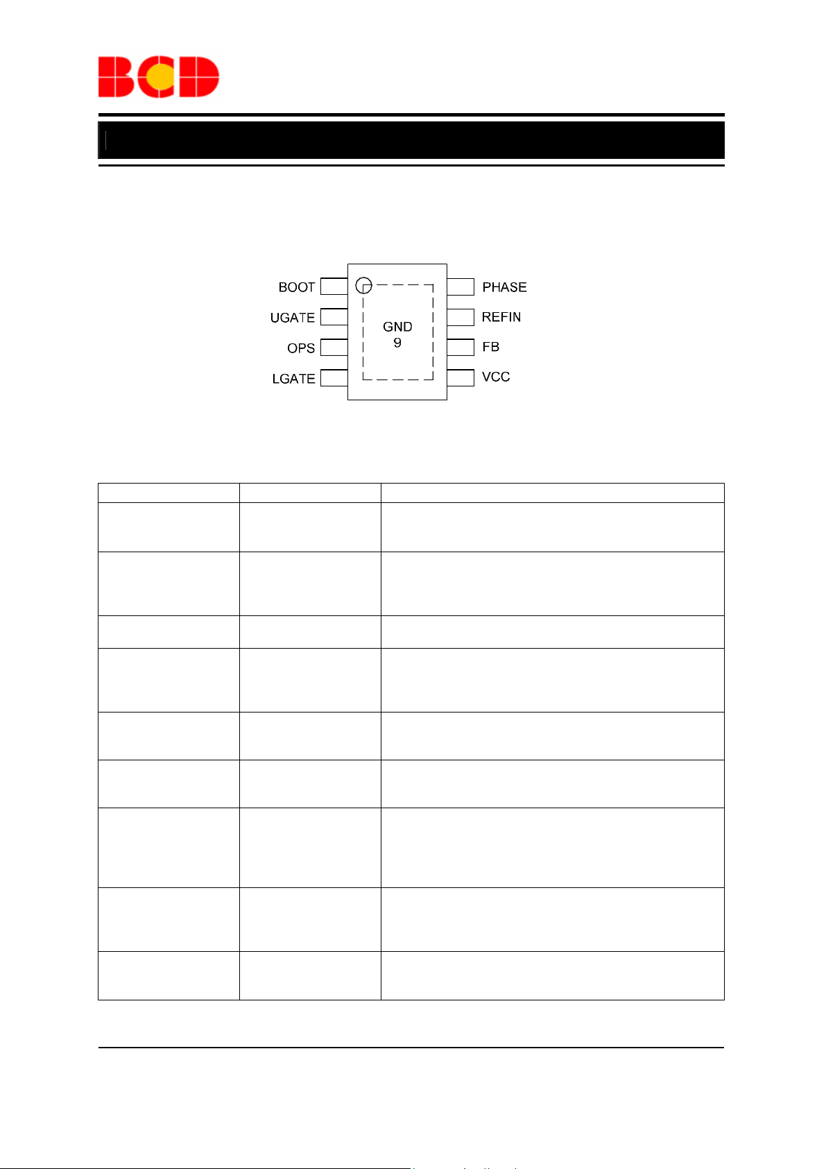
Pin Configuration
MP Package
(PSOP-8)
1
2
3
4
Figure 2. Pin Configuration of AP3583/A (Top View)
8
7
6
5
Pin Description
Pin Number Pin Name Function
Bootstrap pin. Connect a bootstrap capacitor (Typically from 0.1
1 BOOT
2 UGATE
3 OPS
4 LGATE
5 VCC
6 FB
7 REFIN
8 PHASE
9 GND
to 0.47µF) from this pin to PHASE pin to create a BOOT voltage
suitable to drive a standard N-Channel MOSFET
Upper-gate drive pin. Connect this pin to the upper MOSFET gate
roviding the gate drive. This pin is monitored by the adaptive
shoot-through protection circuitry to determine when the upper
MOSFET has been turned off
Over-current setting pin. Connecting a resistor (R
OPS and GND to set the over-current trigger point
Lower-gate drive pin. Connect LGATE to the lower MOSFET
gate providing the gate drive for the lower MOSFET. This pin is
monitored by the adaptive shoot-through protection circuitry to
determine when the lower MOSFET has been turned off
Bias supply pin. Provides a 5V or 12V bias supply for the chip
from this pin. The pin should be bypassed with a capacitor to
GND
Feedback pin. This pin is the inverting input of the internal error
amplifier. A resistor divider from output to GND is used to set the
output voltage
External reference input pin. This pin receives a voltage with
range from 0.4V to 3.0V as the reference voltage at the
non-inverting input of the error amplifier. Pull this pin lower than
0.3V to disable the controller, and the V
low. Let this pin open for internal 0.6V reference use
PHASE pin. This pin connects to the source of the upper
MOSFET and the drain of the lower MOSFET. This pin is also
monitored by the adaptive shoot-through protection circuitry to
determine when the upper MOSFET is turned off
Exposed pad as ground pin. Represents the signal and power
ground for the IC. Tie this pin to ground island/plane through the
lowest impedance connection available
) between
OCSET
UGATE
and V
LGATE
will go
Dec. 2011 Rev. 1. 1 BCD Semiconductor Manufacturing Limited
2
Page 3
Data Sheet
Single Phase Synchronous Buck PWM Controller With Reference Input AP3583/A
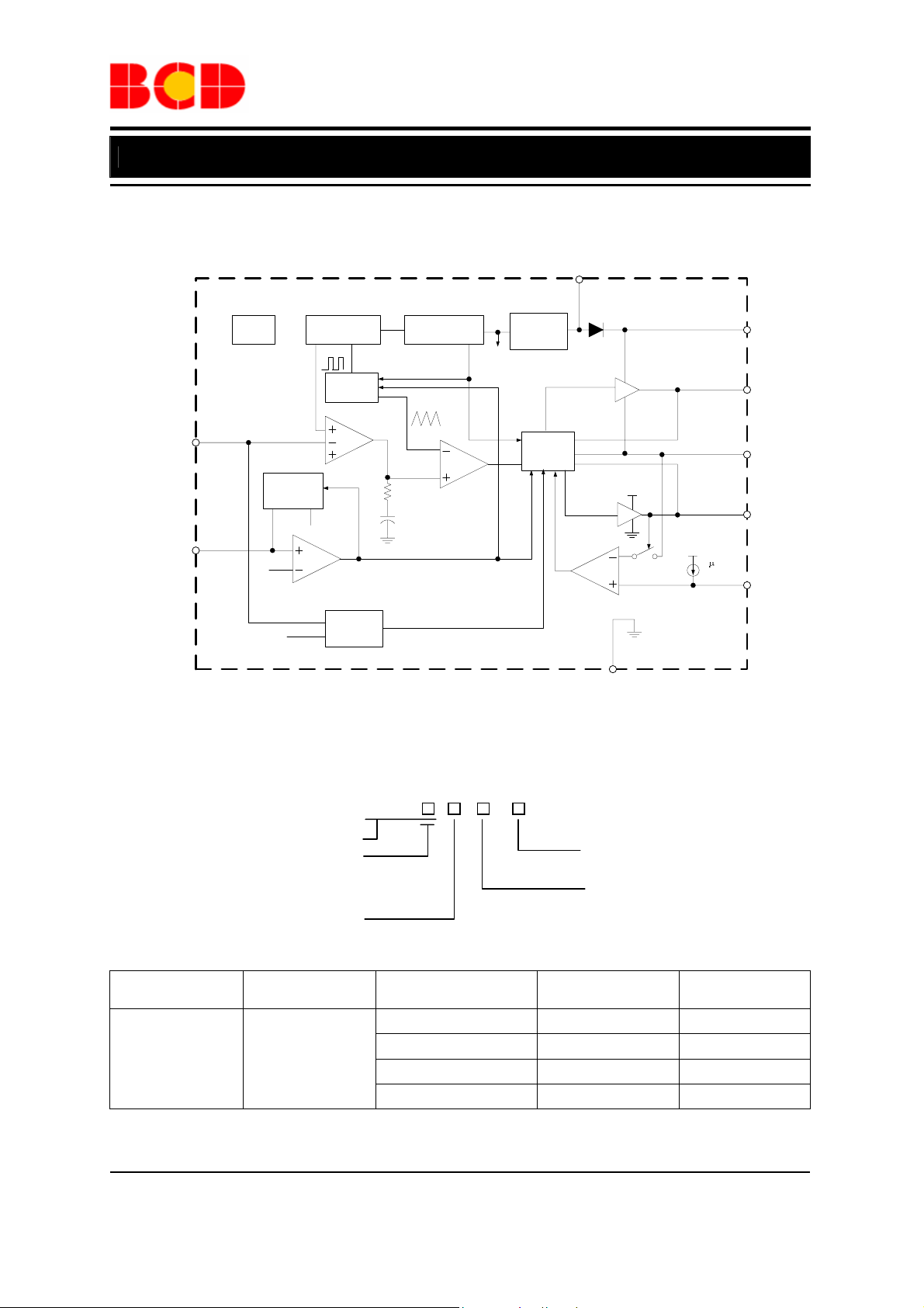
Functional Block Diagram
VCC
5
1
BOOT
2
UGATE
8
PHASE
4
LGATE
A
40
3
OPS
4V INT
PWM
INTERNAL
REGULATOR
GATE
CONTROL
LOGIC
OCP
COMPARATOR
VCC
9
FB
REFIN
OTP
6
REFERENCE
SELECTION
7
0.3V
137.5%V
SOFT-START
OSCILLATOR
ERROR
AMPLIFIER
0.6V
ENABLE
REF
OVP
POWER-ON RESET
(POR)
PWM
COMPARATOR
GND
Figure 3. Functional Block Diagram of AP3583/A
Ordering Information
AP3583 -
Circuit Type
Blank: AP3583
A: AP3583A
Package
MP: PSOP-8
Package
Temperature
Range
Part Number Marking ID Packing Type
AP3583MP-G1 3583MP-G1 Tube
PSOP-8 -40 to 85°C
AP3583MPTR-G1 3583MP-G1 Tape & Reel
AP3583AMP-G1 3583AMP-G1 Tube
AP3583AMPTR-G1 3583AMP-G1 Tape & Reel
BCD Semiconductor's Pb-free products, as designated with "G1" suffix in the part number, are RoHS compliant
and green.
Dec. 2011 Rev. 1. 1 BCD Semiconductor Manufacturing Limited
3
G1: Green
Blank: Tube
TR: Tape & Reel
Page 4
Data Sheet
Single Phase Synchronous Buck PWM Controller With Reference Input AP3583/A
Absolute Maximum Ratings (Note 1)
Parameter Symbol Value Unit
Supply Voltage VCC -0.3 to 15 V
BOOT Voltage V
Voltage from UGATE to PHASE
Voltage from PHASE, LGATE Pin to GND
Voltage on Other Separate Pin
Thermal Resistance
Operating Junction Temperature
Storage Temperature
Lead Temperature (Soldering, 10 sec)
ESD (Human Body Model) (Note 2) 2000 V
ESD (Machine Model) (Note 2) 200 V
-0.3 to V
BOOT
V
UGATE
V
,
PHASE
V
LGATE
θ
JA
T
J
T
STG
T
LEAD
+15 V
PHASE
-0.3 to 15 V
-1 to 15 V
-0.3 to 6 V
50 ºC/W
-40 to 125 ºC
-65 to 150 ºC
260 ºC
Note 1: Stresses greater than those listed under “Absolute Maximum Ratings” may cause permanent damage to
the device. These are stress ratings only, and functional operation of the device at these or any other conditions
beyond those indicated under “Recommended Operating Conditions” is not implied. Exposure to “Absolute
Maximum Ratings” for extended periods may affect device reliability.
Note 2: Devices are ESD sensitive. Handling precaution recommended.
Recommended Operating Conditions
Parameter Symbol Min Max Unit
Supply Input Voltage VCC 4.5 13.2 V
Operating Junction Temperature TJ -40 125
Operating Ambient Temperature TA -40 85
°C
°C
Dec. 2011 Rev. 1. 1 BCD Semiconductor Manufacturing Limited
4
Page 5

Data Sheet
Single Phase Synchronous Buck PWM Controller With Reference Input AP3583/A
Electrical Characteristics
VCC=12V, TA=25°C, unless otherwise specified.
Parameter Symbol Conditions Min Typ Max Unit
SUPPLY INPUT
Supply Voltage VCC 4.5 13.2 V
UGATE1and1LGATE
Supply Current ICC
Quiescent Supply Current I
CC_Q
Power Input Voltage VIN 3.0 13.2 V
POWER ON RESET
VCC Rising Threshold V
VCC Threshold Hysteresis V
POR
POR_HYS
OSCILLATOR
Oscillator Frequency f
Ramp Amplitude ∆V
OSC
OSC
PWM CONTROLLER GATE DRIVERS
Upper Gate Source Current I
Upper Gate Sink Current I
Upper Gate Sink Resistance R
Lower Gate Source Current I
Lower Gate Sink Current I
Lower Gate Sink Resistance R
PHASE Falling to LGATE
Rising Delay
LGATE Falling to UGATE
Rising Delay
UG_SRC
UG_SNK
UGATE
LG_SRC
LG_SNK
LGATE
Minimum Duty Cycle 0 %
Maximum Duty Cycle 75 80 85 %
REFERENCE VOLTAGE
Feedback Voltage VFB Stand-alone Mode 0.591 0.6 0.609 V
Pin1Open;
V
CC
V
FB=VREF
No Switching
=12V,1Switching
+0.1V,
3 mA
2 mA
VCC Rising 4.0 4.2 4.4 V
300 mV
AP3583 180 200 220
AP3583A 270 300 330
kHz
VCC=12V 1.0 V
V
BOOT-VPHASE
V
BOOT-VUGATE
V
BOOT-VPHASE
V
BOOT-VUGATE
50mA Sink Current
V
BOOT-VPHASE
VCC-V
V
LGATE
=6V 1.5 A
LGATE
=12V,
V
CC
50mA Source Current
V
<1.2V to
PHASE
V
>1.2V
LGATE
<1.2V to
V
LGATE
(V
UGATE-VPHASE
=12V,
=6V
=12V,
=6V
=12V
-1 A
1.5 A
1.6 3.2
Ω
=6V -1 A
1 2
Ω
50 ns
)>1.2V
50 ns
Dec. 2011 Rev. 1. 1 BCD Semiconductor Manufacturing Limited
5
Page 6

Data Sheet
Single Phase Synchronous Buck PWM Controller With Reference Input AP3583/A
Electrical Characteristics (Continued)
VCC=12V, T
=25℃, unless otherwise specified.
A
Parameter Symbol Conditions Min Typ Max Unit
Output Voltage Accuracy
REFIN Enable Threshold V
REFIN
PROTECTION
Under Voltage Protection V
Over Current Source I
FB_UVP
OPS
Soft-start Interval tSS
Thermal Shutdown T
Thermal Shutdown Hysteresis T
OTSD
HYS
│V
FB-VREFIN
=0.4V to 1.0V,
Tracking Mode
│V
FB-VREFIN
V
REFIN
Tracking Mode
0.3 0.35 V
30 40 50
AP3583,1Stand-alone
Mode
AP3583A,1Stand-alone
Mode
160 ºC
20 ºC
│,1V
REFIN
15 mV
│/V
=1.0V to 3.0V,
REFIN
,
1.5 %
0.3 0.4 0.5 V
µA
2.6
ms
2.0
Typical Performance Characteristics
0.4
0.3
0.2
0.1
0.0
-0.1
Output Voltage Variation (%)
-0.2
-0.3
4567891011121314
Input Voltage (V)
V
OUT
=1.2V, I
1.0
0.5
0.0
-0.5
-1.0
=10A
OUT
-1.5
-2.0
-2.5
-3.0
Output Voltage Variation (%)
-3.5
-4.0
0 2 4 6 8 10 12 14 16 18 20 22
Output Current (A)
VIN=12V, V
OUT
=1.2V
Figure 4. Line Regulation Figure 5. Load Regulation
Dec. 2011 Rev. 1. 1 BCD Semiconductor Manufacturing Limited
6
Page 7

Data Sheet
Single Phase Synchronous Buck PWM Controller With Reference Input AP3583/A
Typical Performance Characteristics (Continued)
330
320
310
300
290
280
270
260
Switching Frequency (kHz)
250
240
-50 -25 0 25 50 75 100 125 150
Temperature (oC)
For AP3583A
360
350
340
330
320
310
300
290
280
270
Switching Frequency (kHz)
260
250
240
4567891011121314
For AP3583A
Input Voltage (V)
Figure 6. Switching Frequency vs. Temperature Figure 7. Switching Frequency vs. Input Voltage
0.700
0.675
0.650
0.625
0.600
0.575
0.550
Feedback Voltage (V)
0.525
0.500
-50 -25 0 25 50 75 100 125 150
Temperature (oC)
0.605
0.604
0.603
0.602
0.601
0.600
0.599
0.598
Feedback Voltage (V)
0.597
0.596
0.595
4567891011121314
Input Voltage (V)
Figure 8. Feedback Voltage vs. Temperature Figure 9. Feedback Voltage vs. Input Voltage
Dec. 2011 Rev. 1. 1 BCD Semiconductor Manufacturing Limited
7
Page 8

µ
Data Sheet
Single Phase Synchronous Buck PWM Controller With Reference Input AP3583/A
Typical Performance Characteristics (Continued)
VIN
10V/div
V
OUT
0.5V/div
10A/div
(V
0.5V/div
10A/div
V
LGATE
5V/div
I
L
V
REFIN
5V/div
V
OUT
V
PHASE
10V/div
I
L
Figure 12. Enable Waveform
(VIN=12V, V
Time 1ms/div
Figure 10. Power-on Waveform Figure 11. Power-off Waveform
=12V, V
IN
OUT
=1.2V, I
=0A) (VIN=12V, V
OUT
Time 1ms/div
=0A) (VIN=12V, V
OUT
OUT
=1.2V, I
V
IN
10V/div
V
OUT
0.5V/div
V
LGATE
5V/div
I
5A/div
V
REFIN
5V/div
V
OUT
0.5V/div
V
PHASE
10V/div
10A/div
L
Time 200ms/div
OUT
=1.2V, I
=0A)
OUT
I
L
Time 40
Figure 13. Disable Waveform
OUT
s/div
=1.2V, I
OUT
=20A)
Dec. 2011 Rev. 1. 1 BCD Semiconductor Manufacturing Limited
8
Page 9

Data Sheet
Single Phase Synchronous Buck PWM Controller With Reference Input AP3583/A
Typical Performance Characteristics (Continued)
V
OUT
2V/div
V
REFIN
2V/div
V
LGATE
10V/div
0.5V/div
10V/div
V
IN
5V/div
V
OUT
V
LGATE
I
10A/div
L
Time 10ms/div
Time 1ms/div
Figure 14. REFIN Operation
(VIN=12V, V
OUT
=1.2V, I
Figure 15. Power Input Detection
=5A) (VIN=12V, V
OUT
OUT
=1.2V, I
OUT
=0A)
V
UGATE-PHASE
2V/div
V
UGATE-PHASE
2V/div
V
V
PHASE
2V/div
V
UGATE
5V/div
V
LGATE
2V/div
Figure 16. UGATE Turn-off Waveforms Figure 17. UGATE Turn-on Waveforms
(VIN=12V, V
Time 40ns/div
=1.2V, I
OUT
=20A) (VIN=12V, V
OUT
LGATE
2V/div
V
UGATE
5V/div
V
PHASE
2V/div
Time 40ns/div
OUT
=1.2V, I
OUT
=20A)
Dec. 2011 Rev. 1. 1 BCD Semiconductor Manufacturing Limited
9
Page 10

Data Sheet
Single Phase Synchronous Buck PWM Controller With Reference Input AP3583/A
Typical Performance Characteristics (Continued)
V
V
PHASE
5V/div
PHASE
5V/div
V
(AC)
OUT
200mV/div
V
(AC)
OUT
200mV/div
I
OUT
5A/div
Time 10µs/div
I
OUT
10A/div
Time 10µs/div
Figure 18. Load Transient Response Figure 19. Load Transient Response
(V
=12V, V
IN
OUT
=1.2V, I
=0 to 10A; 4A/µs) (VIN=12V, V
OUT
OUT
=1.2V, I
=0 to 20A; 4A/µs)
OUT
V
OUT
0.5V/div
V
PHASE
10V/div
10A/div
IL
Time 20ms/div
V
FB
1V/div
V
UGATE
20V/div
V
LGATE
10V/div
I
10A/div
L
Time 80µs/div
Figure 20. Over Current Protection Figure 21. Over Voltage Protection
(VIN=12V, V
=1.2V to 0V, I
OUT
=0A) (VIN=12V, V
OUT
OUT
=1.2V, I
OUT
=0A)
Dec. 2011 Rev. 1. 1 BCD Semiconductor Manufacturing Limited
10
Page 11

Data Sheet
Single Phase Synchronous Buck PWM Controller With Reference Input AP3583/A
T ypical Application
Figure 22. Typical Application Circuit of AP3583/A
Dec. 2011 Rev. 1. 1 BCD Semiconductor Manufacturing Limited
11
Page 12

Data Sheet
Single Phase Synchronous Buck PWM Controller With Reference Input AP3583/A
Mechanical Dimensions
PSOP-8 Unit: mm(inch)
3.202(0.126)
3.402(0.134)
Dec. 2011 Rev. 1. 1 BCD Semiconductor Manufacturing Limited
12
Page 13

BCD Semiconductor Manufacturing Limited
IMPORTANT NOTICE
IMPORTANT NOTICE
BCD Semiconductor Manufacturing Limited reserves the right to make changes without further notice to any products or specifi-
BCD Semiconductor Manufacturing Limited reserves the right to make changes without further notice to any products or specifi-
cations herein. BCD Semiconductor Manufacturing Limited does not assume any responsibility for use of any its products for any
cations herein. BCD Semiconductor Manufacturing Limited does not assume any responsibility for use of any its products for any
particular purpose, nor does BCD Semiconductor Manufacturing Limited assume any liability arising out of the application or use
particular purpose, nor does BCD Semiconductor Manufacturing Limited assume any liability arising out of the application or use
of any its products or circuits. BCD Semiconductor Manufacturing Limited does not convey any license under its patent rights or
of any its products or circuits. BCD Semiconductor Manufacturing Limited does not convey any license under its patent rights or
other rights nor the rights of others.
other rights nor the rights of others.
http://www.bcdsemi.com
MAIN SITE
MAIN SITE
- Headquarters
BCD Semiconductor Manufacturing Limited
BCD Semiconductor Manufactur ing Limited
- Wafer Fab
No. 1600, Zi Xing Road, Shanghai ZiZhu Science-based Industrial Park, 200241, China
Shanghai SIM-BCD Semiconductor Manufacturing Limited
Tel: +86-21-24162266, Fax: +86-21-24162277
800, Yi Shan Road, Shanghai 200233, China
Tel: +86-21-6485 1491, Fax: +86-21-5450 0008
REGIONAL SALES OFFICE
Shenzhen Office
REGIONAL SALES OFFICE
Shanghai SIM-BCD Semiconductor Manufacturing Co., Ltd., Shenzhen Office
Shenzhen Office
Unit A Room 1203, Skyworth Bldg., Gaoxin Ave.1.S., Nanshan District, Shenzhen,
Shanghai SIM-BCD Semiconductor Manufacturing Co., Ltd. Shenzhen Office
China
Advanced Analog Circuits (Shanghai) Corporation Shenzhen Office
Tel: +86-755-8826 7951
Room E, 5F, Noble Center, No.1006, 3rd Fuzhong Road, Futian District, Shenzhen 518026, China
Fax: +86-755-8826 7865
Tel: +86-755-8826 7951
Fax: +86-755-8826 7865
- Wafer Fab
BCD Semiconductor Manufacturing Limited
Shanghai SIM-BCD Semiconductor Manufacturing Co., Ltd.
- IC Design Group
800 Yi Shan Road, Shanghai 200233, China
Advanced Analog Circuits (Shanghai) Corporation
Tel: +86-21-6485 1491, Fax: +86-21-5450 0008
8F, Zone B, 900, Yi Shan Road, Shanghai 200233, China
Tel: +86-21-6495 9539, Fax: +86-21-6485 9673
Taiwan Office
BCD Semiconductor (Taiwan) Company Limited
Taiwan Office
4F, 298-1, Rui Guang Road, Nei-Hu District, Taipei,
BCD Semiconductor (Taiwan) Company Limited
Tai wan
4F, 298-1, Rui Guang Road, Nei-Hu District, Taipei,
Tel: +886-2-2656 2808
Taiwan
Fax: +886-2-2656 2806
Tel: +886-2-2656 2808
Fax: +886-2-2656 2806
USA Office
BCD Semiconductor Corp.
USA Office
30920 Huntwood Ave. Hayward,
BCD Semiconductor Corporation
CA 94544, USA
30920 Huntwood Ave. Hayward,
Tel : +1-510-324-2988
CA 94544, U.S.A
Fax: +1-510-324-2788
Tel : +1-510-324-2988
Fax: +1-510-324-2788
 Loading...