Diodes AP3581A, AP3581B, AP3581C User Manual

Single Phase Synchronous Buck PWM Controller AP3581A/B/C
Data Sheet
General Description
The1AP3581A/B/C1is1a1compact1synchronous-rect
ified buck controller specifically designed to operate
from 5V/12V supply and deliver high-quality output
voltage as low as 0.6V (AP3581A) or 0.8V
(AP3581B/C). The AP3581A/B/C operates at fixed
frequency of 300kHz (AP3581A/B) or 200kHz
(AP3581C) and provides an optimal level of
integration to reduce size and cost of the power
supply.
This controller integrates internal MOSFET drivers
that support 12V+12V bootstrapped voltage for highefficiency power conversion. The bootstrap diode is
built-in to simplify the circuit design and minimize
external part count.
This controller provides single feedback loop,
voltage-mode control with fast transient response.
The error amplifier features a 10MHz gain-bandwidth
product and 6V/µs slew rate which enables high
converter bandwidth for fast transient performance.
Other features include internal soft-start, under
voltage protection, over current protection and
shutdown function. With afore-mentioned functions,
this part provides customers a compact, high
efficiency, well-protected and cost-effective
solutions.
The AP3581A/B/C is available in PSOP-8 package.
Figure 1. Package Type of AP3581A/B/C
Features
• Supply Voltage: 5V/12V
• V
• 0.6V/0.8V to 80% of V
• Internal Reference: 0.6V/0.8V
• Simple Single-loop Control
• Voltage-mode PWM Control
• Duty Cycle: 0% to 80%
• Fast Transient Response
• 10MHz High-bandwidth Error Amplifier with
• Fixed Oscillator Frequency: 300kHz/200kHz
• Lossless, Programmable Over Current Protection
• Start-up into Pre-biased Output
• Built-in Thermal Shutdown
• Built-in Soft-start
• Over Current/Voltage Protection
• Under Voltage Protection
• Integrated Boot Diode
Input Range: 3.0V to 13.2V
IN
IN
6V/µs Slew Rate
(Uses Lower MOSFET R
Output Range
)
DS(ON)
Applications
• Power Supplies for Microprocessors/Peripherals
PCs, Embedded Controllers, Memory Supplies
•
• DSP and Core Communications Processor
Supplies
• Subsystem Power Supplies
• PCI, AGP, Graphics Cards, Digital TV
• SSTL-2 and DDR/2/3 SDRAM Bus Termination
Supply
• Cable Modems, Set Top Boxes, and DSL
Modems
• Industrial Power Supplies and General Purpose
Supplies
• 5V/12V Input DC-DC Regulators
• Low-voltage Distributed Power Supplies
PSOP-8
Oct. 2011 Rev. 1. 0 BCD Semiconductor Manufacturing Limited
1

p
Data Sheet
Single Phase Synchronous Buck PWM Controller AP3581A/B/C
Pin Configuration
MP Package
(PSOP-8)
1
2
3
4
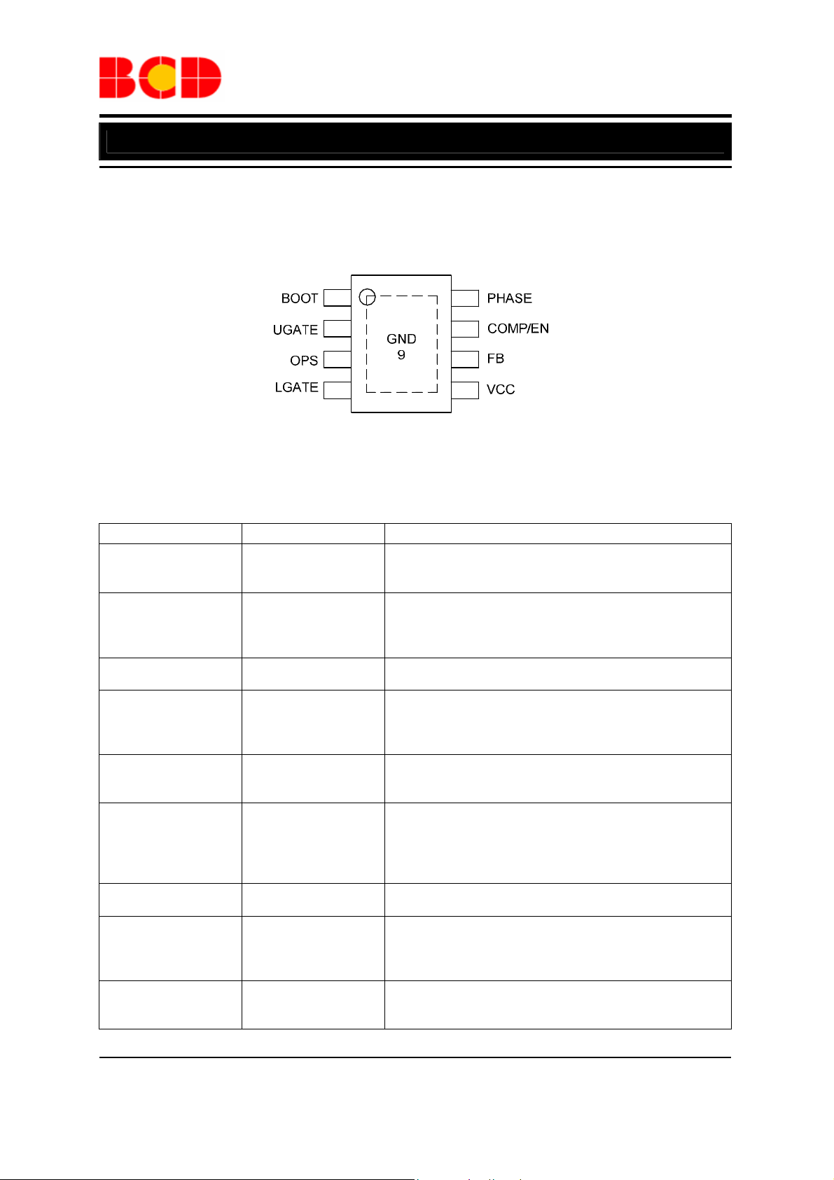
Figure 2. Pin Configuration of AP3581A/B/C (Top View)
8
7
6
5
Pin Description
Pin Number Pin Name Function
Bootstrap pin. Connect a bootstrap capacitor (Typically from
1 BOOT
2 UGATE
3 OPS
4 LGATE
5 VCC
6 FB
7 COMP/EN
8 PHASE
9 GND
0.1µF to 0.47µF) from this pin to PHASE pin to create a BOOT
voltage suitable to drive a standard N-Channel MOSFET
Upper-gate drive pin. Connect this pin to the upper MOSFET gate
roviding the gate drive. This pin is monitored by the adaptive
shoot-through protection circuitry to determine when the upper
MOSFET has been turned off
Over-current setting pin. Connecting a resistor (R
OPS and GND to set the over-current trigger point
Lower-gate drive pin. Connect LGATE to the lower MOSFET
gate providing the gate drive for the lower MOSFET. This pin is
monitored by the adaptive shoot-through protection circuitry to
determine when the lower MOSFET has turned off
Bias supply pin. Provides a 5V or 12V bias supply for the chip
from this pin. The pin should be bypassed with a capacitor to
GND
Feedback pin. This pin is the inverting input of the internal error
amplifier. Use FB pin, in combination with the COMP pin, to
compensate the voltage control feedback loop of the converter. A
resistor divider from output to GND is used to set the output
voltage
Compensation and disable pin, this pin is the output of the error
amplifier. Pull COMP pin low will shut down the IC
PHASE pin. This pin connects to the source of the upper
MOSFET and the drain of the lower MOSFET. This pin is also
monitored by the adaptive shoot-through protection circuitry to
determine when the upper MOSFET has turned off
Exposed pad as ground pin. Represents the signal and power
ground for the IC. Tie this pin to the ground island/plane through
the lowest impedance connection available
) between
OCSET
Oct. 2011 Rev. 1. 0 BCD Semiconductor Manufacturing Limited
2

Data Sheet
Single Phase Synchronous Buck PWM Controller AP3581A/B/C
Functional Block Diagram
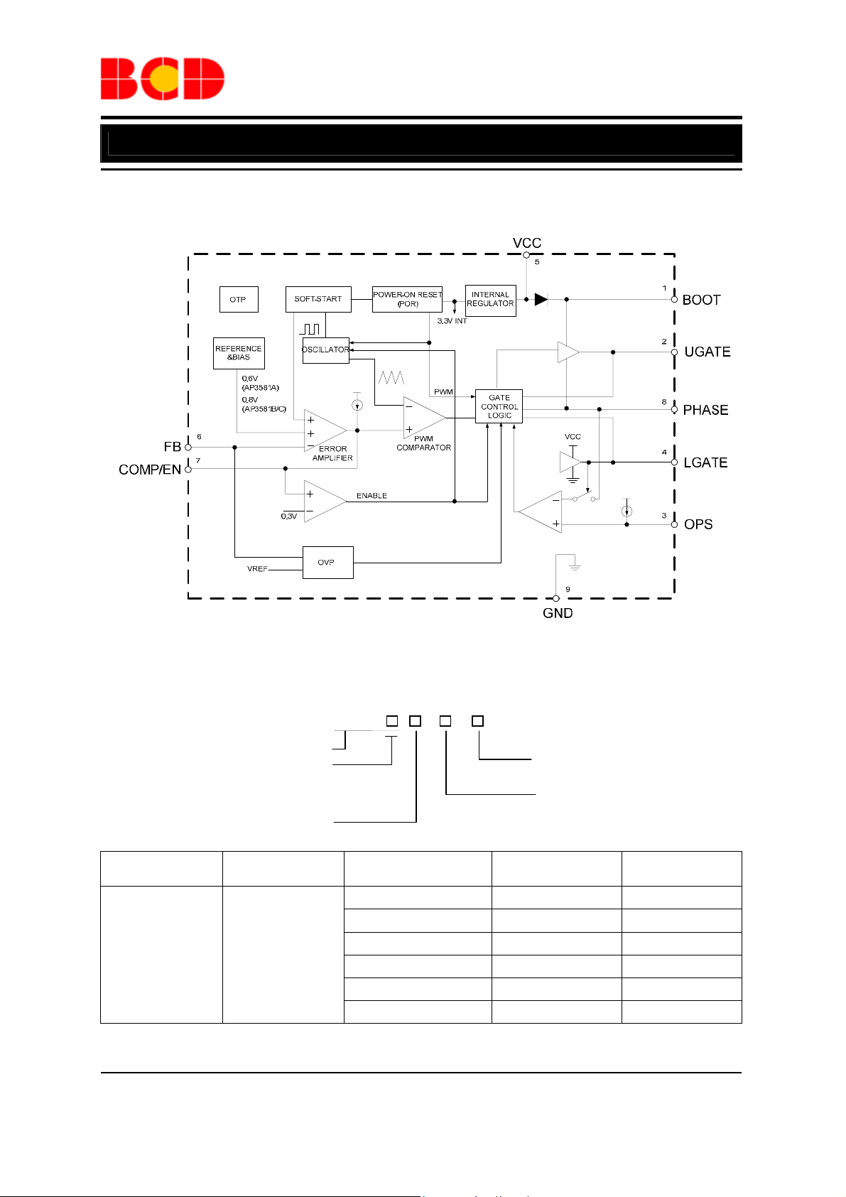
Figure 3. Functional Block Diagram of AP3581A/B/C
Ordering Information
AP3581 A A -
Circuit Type
A:AP3581A
B:AP3581B
C:AP3581C
Package
Package
PSOP-8 -40 to 85°C
BCD Semiconductor's Pb-free products, as designated with "G1" suffix in the part number, are RoHS compliant
and green.
Oct. 2011 Rev. 1. 0 BCD Semiconductor Manufacturing Limited
MP: PSOP-8
Temperature
Range
Part Number Marking ID Packing Type
AP3581AMP-G1 3581AMP-G1 Tube
AP3581AMPTR-G1 3581AMP-G1 Tape & Reel
AP3581BMP-G1 3581BMP-G1 Tube
AP3581BMPTR-G1 3581BMP-G1 Tape & Reel
AP3581CMP-G1 3581CMP-G1 Tube
AP3581CMPTR-G1 3581CMP-G1 Tape & Reel
G1: Green
Blank: Tube
TR: Tape & Reel
3

Data Sheet
Single Phase Synchronous Buck PWM Controller AP3581A/B/C
Absolute Maximum Ratings (Note 1)
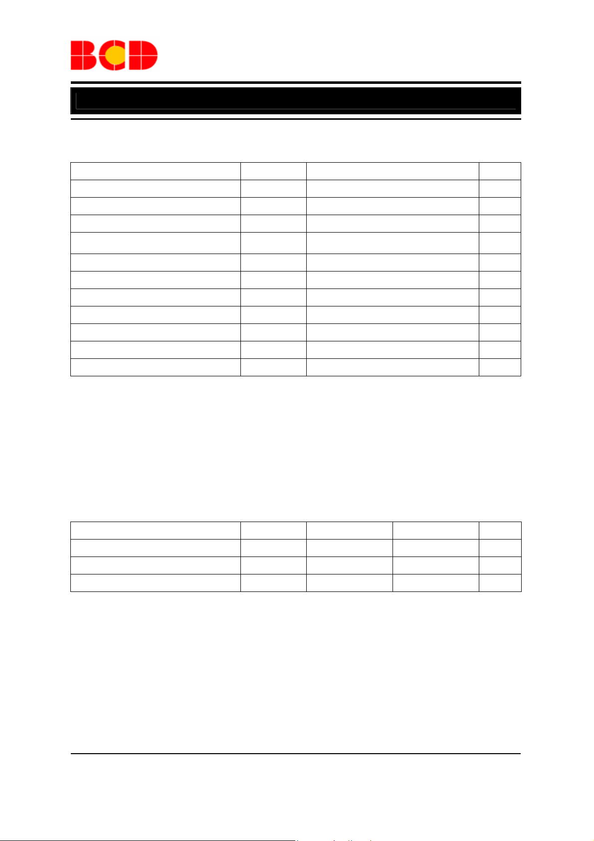
Parameter Symbol Value Unit
Supply Voltage VCC -0.3 to 15 V
BOOT Voltage V
Voltage from UGATE to PHASE
Voltage from PHASE, LGATE Pin to GND
Voltage on Other Separate Pin
Thermal Resistance
Operating Junction Temperature
Storage Temperature
Lead Temperature (Soldering, 10 sec)
ESD (Human Body Model) (Note 2) 2000 V
ESD (Machine Model) (Note 2) 200 V
-0.3 to V
BOOT
V
UGATE
V
,
PHASE
V
LGATE
θ
JA
T
J
T
STG
T
LEAD
+15 V
PHASE
-0.3 to 15 V
-1 to 15 V
-0.3 to 6 V
50 ºC/W
-40 to 125 ºC
-65 to 150 ºC
260 ºC
Note 1: Stresses greater than those listed under “Absolute Maximum Ratings” may cause permanent damage to
the device. These are stress ratings only, and functional operation of the device at these or any other conditions
beyond those indicated under “Recommended Operating Conditions” is not implied. Exposure to “Absolute
Maximum Ratings” for extended periods may affect device reliability.
Note 2: Devices are ESD sensitive. Handling precaution recommended.
Recommended Operating Conditions
Parameter Symbol Min Max Unit
Supply Input Voltage VCC 4.5 13.2 V
Operating Junction Temperature Range TJ -40 125
Operating Ambient Temperature TA -40 85
°C
°C
Oct. 2011 Rev. 1. 0 BCD Semiconductor Manufacturing Limited
4
 Loading...