Diodes AP3036-A User Manual

WHITE LED STEP-UP CONVERTER AP3036/A
Preliminary Datasheet
General Description
The AP3036/A is an inductor-based DC/DC
converter designed to drive up to eight white LEDs in
series for backlight. Only one feedback resistor is
needed to control the LED current and obtain
required brightness.
A constant frequency 1.0MHz PWM control scheme
is employed in this IC, which means tiny external
components can be used. Specifically, 1mm tall
inductor and 0.22µF output capacitor for a typical
application is sufficient. Additionally, the Schottky
diode in boost circuit is integrated on this chip. The
AP3036/A also provides a disable pin to ease its use
for different systems.
The output over-voltage protection is implemented in
AP3036/A. When any LED is broken or in other
abnormal conditions, the output voltage will be
clamped.
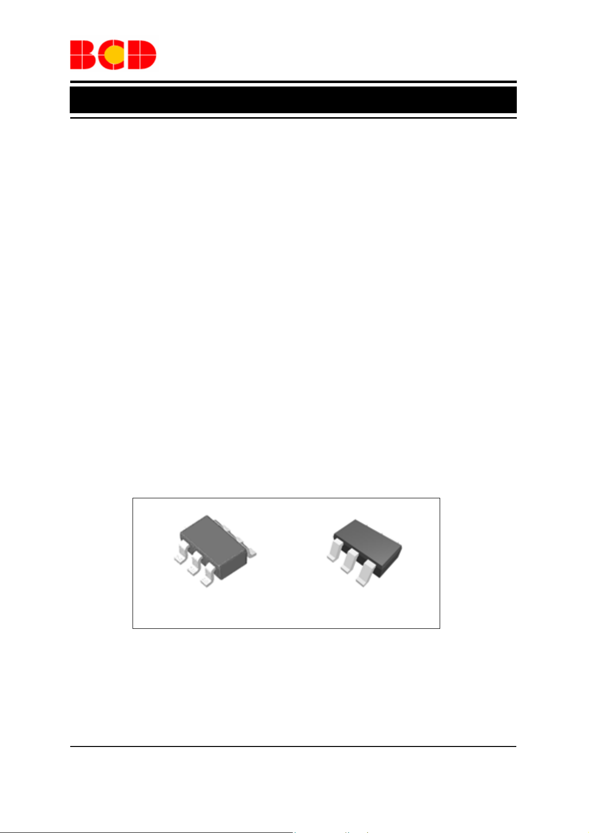
The AP3036/A is available in standard SOT-23-6 and
TSOT-23-6 packages.
Features
Inherently Uniform LED Current
•
• High Efficiency up to 84%
• No Need for External Schottky Diode
• Output Over-voltage Protection (OVP)
• Fixed 1.0MHz Switching Frequency
• Uses Tiny 1mm Tall Inductor
• Requires Only 0.22µF Output Capaci t or
• High Frequency Dimming Control
Applications
• Cellular Phones
• Digital Cameras
• LCD Modules
• GPS Receivers
• PDAs, Handheld Computers
SOT-23-6 TSOT-23-6
Figure 1. Package Types of AP3036/A
Jul. 2012 Rev. 1.3. BCD Semiconductor Manufacturing Limited
1

Preliminary Datasheet
WHITE LED STEP-UP CONVERTER AP3036/A
Pin Configuration
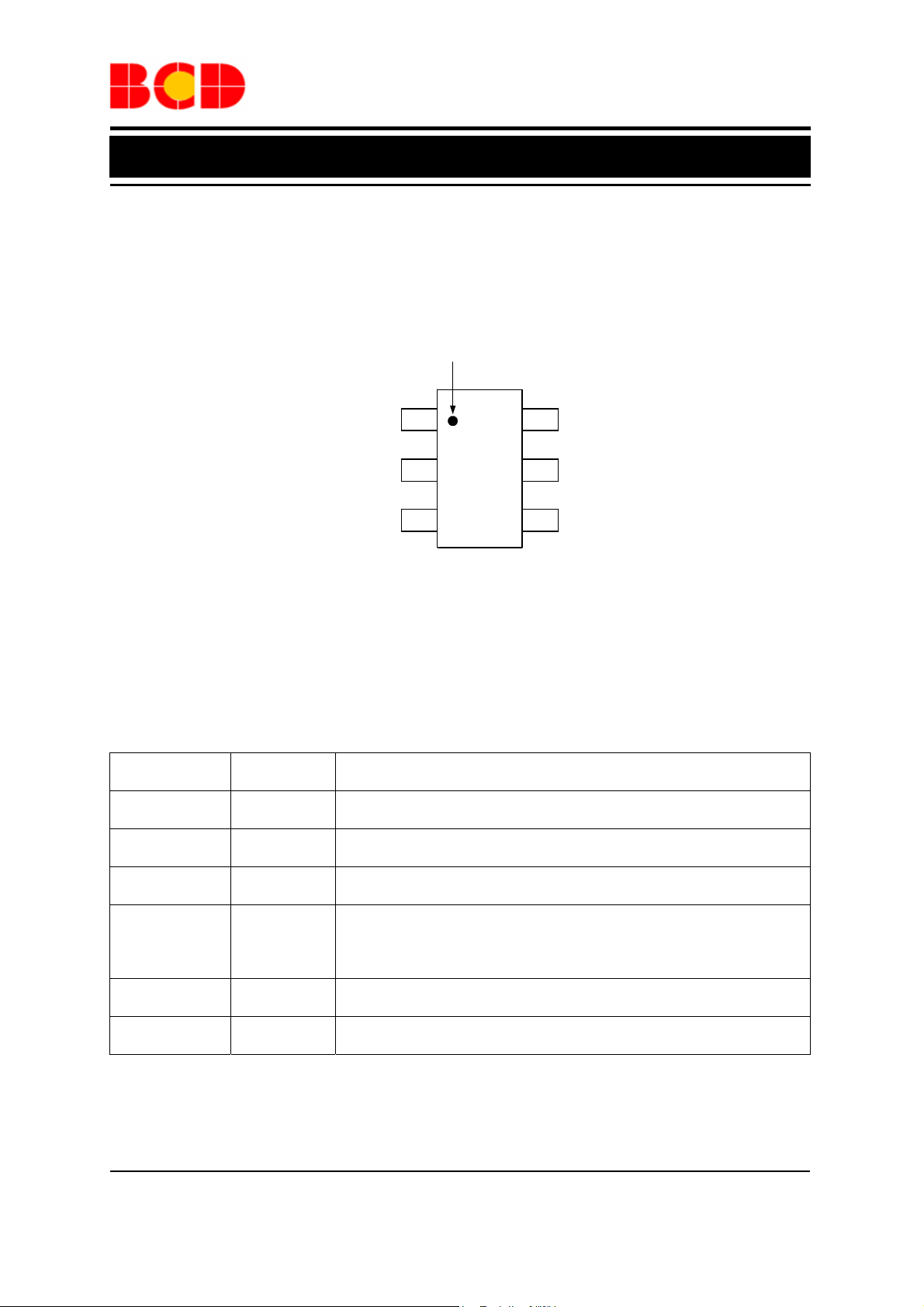
K/KT Package
(SOT-23-6/TSOT-23-6)
GND
Figure 2. Pin Configuration of AP3036/A (Top View)
Pin 1 Dot by Marking
SW
FB
1
2
34
VIN
6
5
VOUT
CTRL
Pin Description
Pin Number Pin Name Function
1 SW
2 GND
3 FB
4 CTRL
5 VOUT
6 VIN
Switch pin. Connect external inductor
Ground
Voltage feedback pin. The reference voltage is 200mV for AP3036
and 250mV for AP3036A
Shutdown and dimming pin. Connect to 1.8V or higher to enable
device; Connect to 0.4V or less to disable device; Connect to a PWM
signal to achieve LEDs brightness dimming
Output pin. Connect to the cathode of internal Schottky diode
Input supply pin. Must be connected to a local bypass capacitor
Jul. 2012 Rev. 1.3. BCD Semiconductor Manufacturing Limited
2

Preliminary Datasheet
WHITE LED STEP-UP CONVERTER AP3036/A
Functional Block Diagram
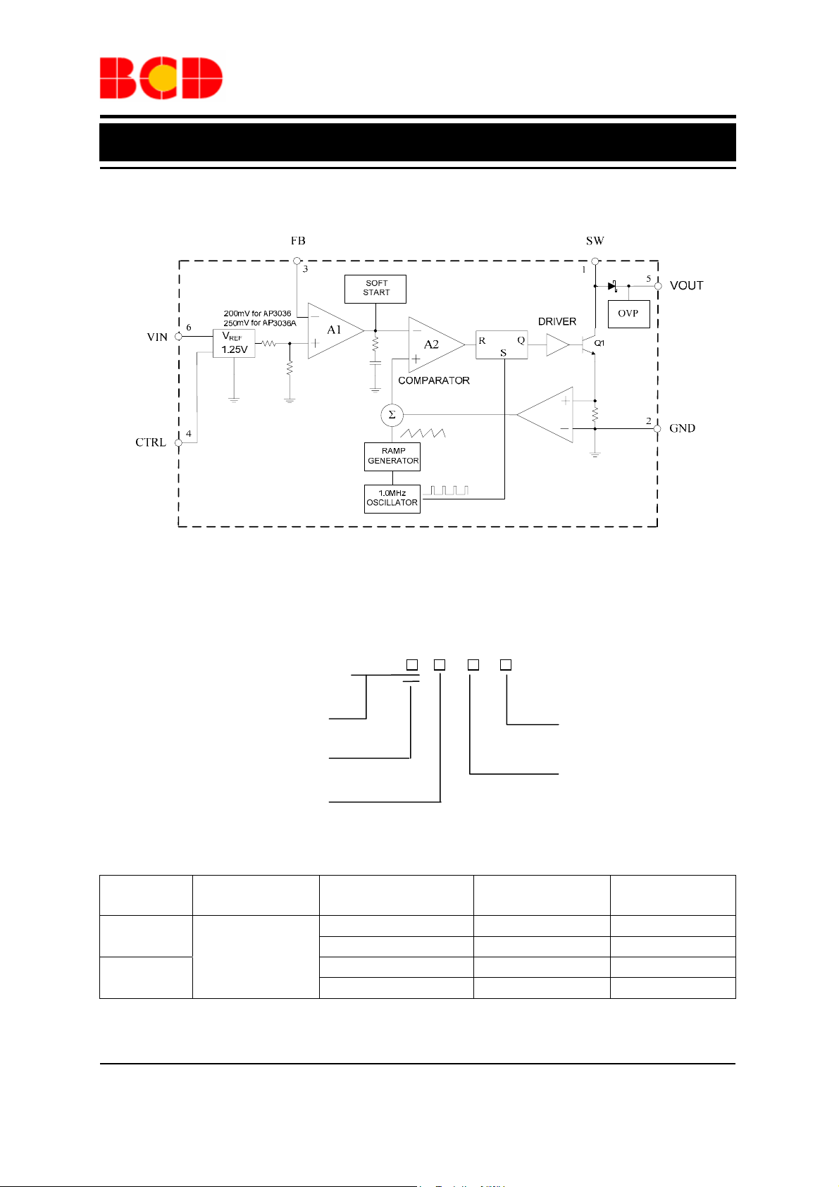
Figure 3. Functional Block Diagram of AP3036/A
Ordering Information
AP3036 -
Circuit Type
Blank: AP3036
A: AP3036A TR: Tape & Reel
Package
K: SOT-23-6
KT: TSOT-23-6
Package
SOT-23-6
TSOT-23-6
Temperature
Range
-40 to 85°C
Part Number Marking ID Packing Type
AP3036KTR-G1 GHI Tape & Reel
AP3036AKTR-G1 GJE Tape & Reel
AP3036KTTR-G1 L2C Tape & Reel
AP3036AKTTR-G1 L3C Tape & Reel
BCD Semiconductor's Pb-free products, as designated with "G1" suffix in the part number, are RoHS compliant
and green.
Jul. 2012 Rev. 1.3. BCD Semiconductor Manufacturing Limited
3
G1: Green

Preliminary Datasheet
WHITE LED STEP-UP CONVERTER AP3036/A
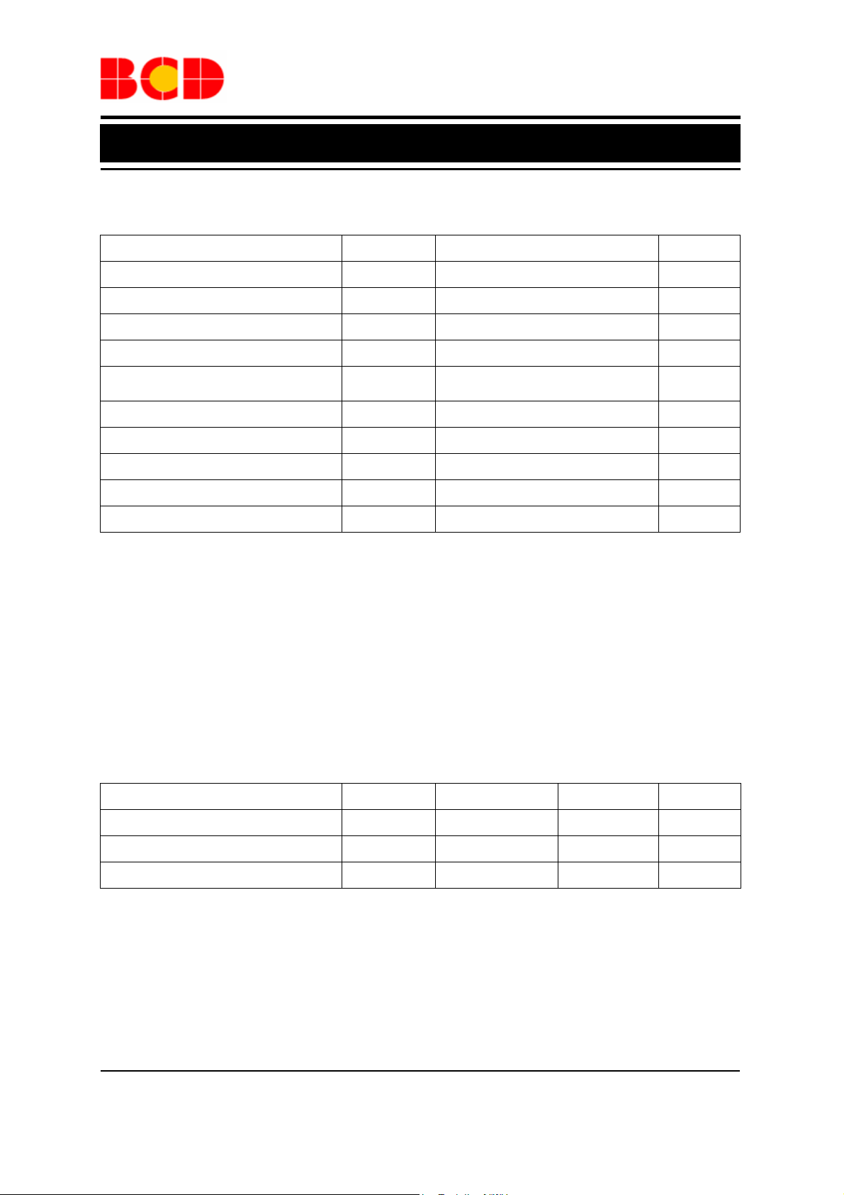
Absolute Maximum Ratings (Note 1)
Parameter Symbol Value Unit
Input Voltage VIN 20 V
SW Pin Voltage VSW 38 V
Feedback Voltage VFB 20 V
CTRL Pin Voltage V
Thermal Resistance (Junction to
Ambient, No Heat Sink)
Operating Junction Temperature TJ 150
Storage Temperature Range T
Lead T em perature (Soldering, 10sec) T
ESD (Machine Model) 250 V
ESD (Human Body Model) 2000 V
20 V
CTRL
θ
JA
-65 to 150
STG
260
LEAD
265
°C/W
°C
°C
°C
Note 1: Stresses greater than those listed under “Absolute Maximu m Ratings” may cause permanent damage to
the device. These are stress ratings only, and functional operation of the device at these or any other conditions
beyond those indicated under “Recommended Operating Conditions” is not implied. Exposure to “Absolute
Maximum Ratings” for extended periods may affect device reliability.
Recommended Operating Conditions
Parameter Symbol Min Max Unit
Operating T em perature Range TOP -40 85
Input Voltage VIN 2.5 16 V
CTRL Pin Voltage V
16 V
CTRL
°C
Jul. 2012 Rev. 1.3. BCD Semiconductor Manufacturing Limited
4

Preliminary Datasheet
WHITE LED STEP-UP CONVERTER AP3036/A
Electrical Characteristics
V
=3V, V
IN
Parameter Symbol Conditions Min Typ Max Unit
Minimum Operating Voltage VIN (Min) 2.5
Maximum Operating Voltage VIN (Max) 16
=3V, TA=25°C, unless otherwise specified.
CTRL
V
Feedback Voltage VFB
AP3036
AP3036A 235 250 265
I
=20mA, 4 LEDs
OUT
188 200 212
mV
FB Pin Bias Current IFB 35 100 nA
Quiescent Current IQ
Shutdown Quiescent Current I
SHDN
V
VFB=VIN, No
Switching
=0V 45 75
CTRL
1.6 3.1 3.9 mA
µA
Switching Frequency f 1.0 MHz
Maximum Duty Cycle D
Switch Current Limit (Note 2) I
Switch VCE Saturation Voltage V
Switch Leakage Current VSW=5V 0.01 5
90 93 %
MAX
D=40% or 80% 550 mA
LIMIT
I
CESAT
=250mA 360 mV
SW
µA
High 1.8
CTRL Pin Voltage V
CTRL
V
Low 0.4
CTRL Pin Bias Current I
CTRL
100
µA
OVP Voltage VOV 30 V
Schottky Forward Drop V
Schottky Leakage Current
Soft Start Time t 100
Thermal Resistance
(Junction to Case)
I
DROP
θ
JC
=150mA 0.7 V
D
(Reverse
V
R
Voltage)=23V
VR(Reverse
Voltage)=27V
0.1 4
µA
150
µs
SOT-23-6 60
°C/W
TSOT-23-6 60
Note 2: The switch current limit is related to duty cycle. Please refer to Figure 16 for detail.
Jul. 2012 Rev. 1.3. BCD Semiconductor Manufacturing Limited
5
 Loading...