

Page 1

Ultra Low Output Voltage Linear N-FET Controller AP2160
Preliminary Datasheet
General Description
The AP2160 is an ultra low output voltage N-FET
linear regulator controller. The output voltage can be
adjusted down to 0.5V. A Power-On-Reset (POR)
circuit monitors supply voltage to prevent wrong
operations. A POK pin indicates the output status. It
can control other converters for power sequence. The
AP2160 can be enabled by other power systems.
The AP2160 integrates a 0.5V reference voltage with
1% accuracy to provide tight regulation to the output
voltage. The regulator also features enable control,
open drain power good signal, under-voltage
protection and soft start.
The AP2160 is available in 6-pin SOT-23-6 standard
package.
Features
0.5V Reference Voltage with 1% Accuracy
•
• Adjustable Output Voltage down to 0.5V
• Low ESR Output Capacitor (MLCC and
POSCAP) Applicable
• Enable Control for the Output Voltage and Low
Shutdown Current
• Under-voltage Short Circuit Protection
• Fast Transient Response
• Power Good Monitoring and Signaling for the
Output
• Drive N-Channel MOSFETs
Applications
• Notebook PC Computers
• Desktop Computers
• Battery Powered Devices
• Portable Instruments
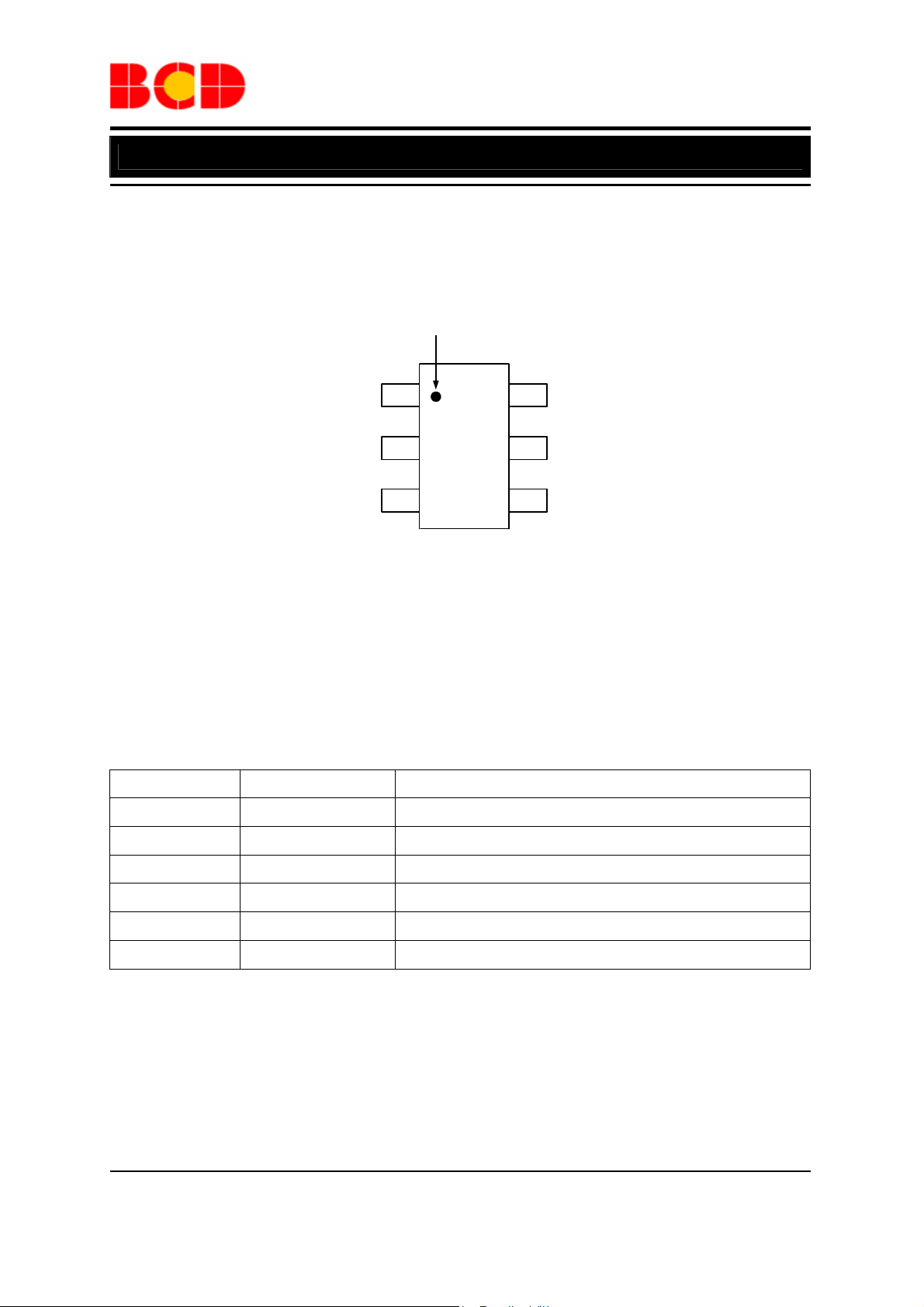
Figure 1. Package Type of AP2160
SOT-23-6
Jan. 2012 Rev. 1. 0 BCD Semiconductor Manufacturing Limited
1
Page 2
Preliminary Datasheet
Ultra Low Output Voltage Linear N-FET Controller AP2160
Pin Configuration
K Package
(SOT-23-6)
VCC DRV
GND FB
POK EN
Figure 2. Pin Configuration of AP2160 (Top View)
Pin 1 Mark
1
2
34
6
5
Pin Description
Pin Number Pin Name Function
1 VCC Input voltage
2 GND Common ground pin
3 POK Power OK output pin
4 EN H: Normal operation; L: Shutdown
5 FB Output voltage feedback pin
6 DRV Gate drive to N-FET
Jan. 2012 Rev. 1. 0 BCD Semiconductor Manufacturing Limited
2
Page 3
Preliminary Datasheet
Ultra Low Output Voltage Linear N-FET Controller AP2160
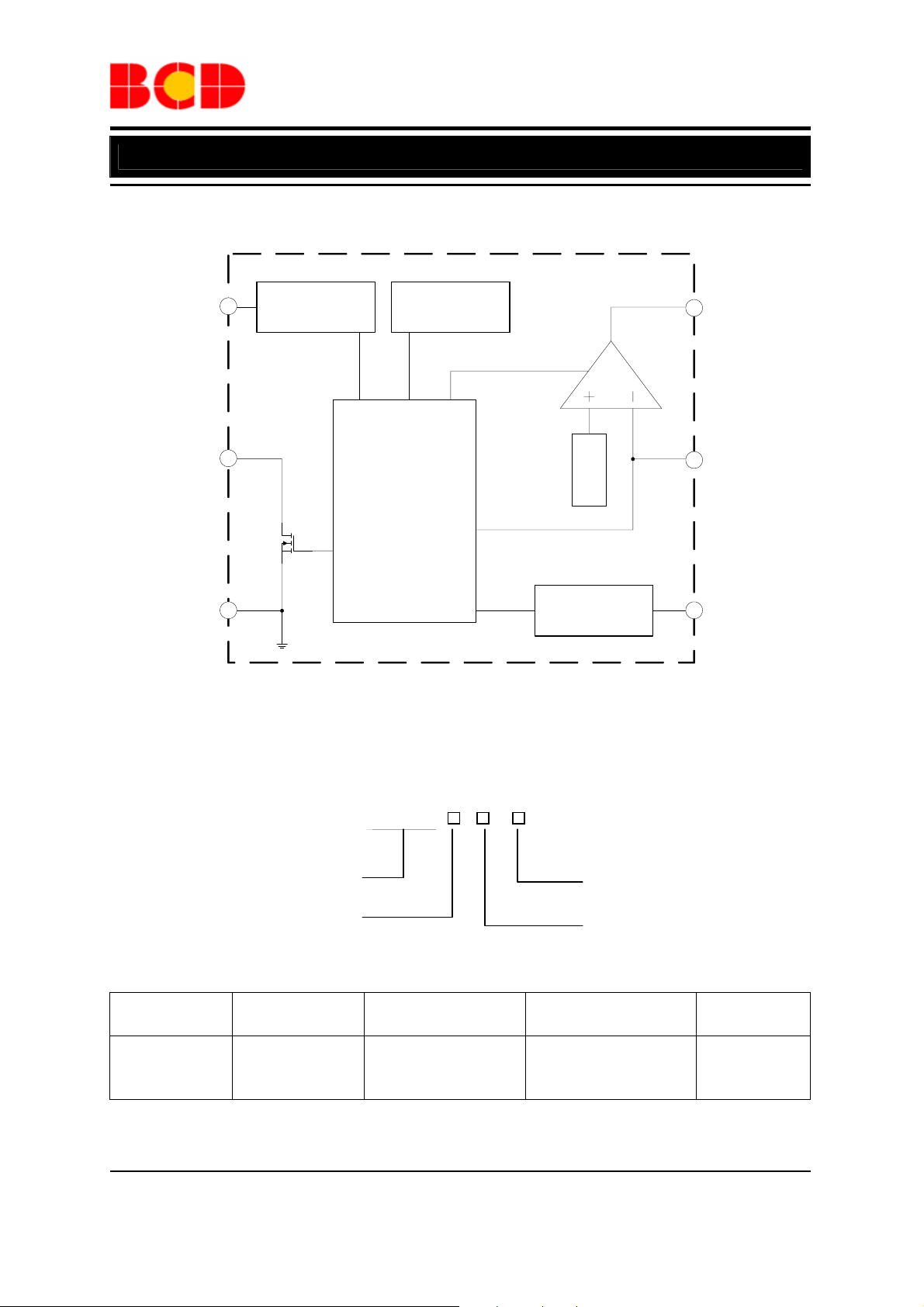
Functional Block Diagram
1
POK
GND
Power On ResetVCC
3
Control Logic Unit
2
Figure 3. Functional Block Diagram of AP2160
Thermal
Protection
Band Gap
Enable Control
6
DRV
5
FB
4
EN
Ordering Information
AP2160 -
Circuit Type G1: Green
Package TR: Tape & Reel
K: SOT-23-6
Package
SOT-23-6
Temperature
Range
-40 to 85°C
Part Number Marking ID
AP2160KTR-G1 GJC Tape & Reel
BCD Semiconductor's Pb-free products, as designated with "G1" suffix in the part number, are RoHS compliant
and green.
Jan. 2012 Rev. 1. 0 BCD Semiconductor Manufacturing Limited
3
Packing
Type
Page 4

Preliminary Datasheet
Ultra Low Output Voltage Linear N-FET Controller AP2160
Absolute Maximum Ratings (Note 1)
Parameter Symbol Value Unit
VCC to GND VCC -0.3 to 7 V
DRV to GND V
POK to GND V
FB to GND VFB -0.3 to VCC+0.3 V
EN to GND VEN -0.3 to VCC+0.3 V
Operating Junction Temperature TJ 150 ºC
Power Dissipation (25ºC) PD 0.4 W
Operating T em perature Range T
Storage Temperature Range T
Lead Temperature (Soldering, 10
Seconds)
ESD (Machine Model)
ESD (Human Body Model)
Note 1: Stresses greater than those listed under “Absolute Maximum Ratings” may cause permanent damage to
the device. These are stress ratings only, and functional operation of the device at these or any other conditions
beyond those indicated under “Recommended Operating Conditions” is not implied. Exposure to “Absolute
Maximum Ratings” for extended periods may affect device reliability.
-0.3 to VCC+0.3 V
DRV
-0.3 to VCC+0.3 V
POK
-40 to 85 ºC
OPR
-65 to 150 ºC
STG
T
LEAD
260 ºC
200 V
2000 V
Recommended Operating Conditions
Parameter Symbol Min Max Unit
Supply Voltage (between VCC and GND) VCC 4.5 5.5 V
System Input Voltage (between VIN and GND) VIN 0.5 5.5 V
Ambient Operating Temperature Range TA -40 85
°C
Jan. 2012 Rev. 1. 0 BCD Semiconductor Manufacturing Limited
4
Page 5

Preliminary Datasheet
Ultra Low Output Voltage Linear N-FET Controller AP2160
Electrical Characteristics
V
=1.5V, V
IN
Parameter Symbol Conditions Min Typ Max Units
Supply Voltage Range VCC 4.5 5.5 V
Input Voltage UVLO
Threshold
Input Voltage UVLO
Hysteresis
Supply Current ICC VEN=VCC=5V 0.42 0.6 mA
=1.05V, VEN=VCC, TA=25°C, CIN=4.7µF, C
OUT
VFB=0.48V, VCC rising 3.70 V
V
UVLO
VFB=0.48V, VCC falling 0.25 V
V
HYST
=22µF, unless otherwise specified.
OUT
Shutdown Current ISD VEN=0V -1 1
µΑ
Feedback Voltage VFB VEN=VCC=5V 0.495 0.5 0.505 V
Feedback Pin Input
Current
EN Pin Logic High
Threshold Voltage
EN Pin Input Current IEN I
Output Voltage UVLO
Threshold
DRV Output Current
VFB=0.5V -100 100 nA
I
FB
V
VCC=5V, VEN rising 1.3
EN-H
V
V
VCC=5V, VEN falling 0.5
EN-L
V
TH(UV)
I
DRV(SS)
I
DRV(SRC)
=0mA, VIN=5V -1 1
OUT
V
Falling 0.2 0.25 0.3 V
FB
Sourcing, VFB=0V 20
Sourcing, VFB=0.48V 2.2
µΑ
µΑ
mA
I
DRV(SINK)
DRV Pin Output Voltage V
POK Threshold Voltage
for Power not OK
V
Sinking, VFB=0.52V 9.0
VFB=0.48V,
DRV
PNOK
V
FB
V
EN=VCC
VFB falling 84% 88% 91% VFB
V
EN=VCC
=5V
=0.52V,
=5V
4.9 5.0
0.8 1.15 1.5
V
POK Low Voltage POK sinks 1mA 200 250 mV
POK Delay Time t
Thermal Shutdown
Temperature
Thermal Shutdown
Hysteresis
0.8 2 10 ms
DELAY
150
T
SD
40
°C
°C
Jan. 2012 Rev. 1. 0 BCD Semiconductor Manufacturing Limited
5
Page 6

Preliminary Datasheet
Ultra Low Output Voltage Linear N-FET Controller AP2160
Typical Performance Characteristics
0.504
0.502
0.500
0.498
Feedback Voltage (V)
0.496
-40-200 20406080100120
Ambient Temperature (oC)
Figure 4. Feedback Voltage vs. Ambient Temperature Figure 5. Supply Current vs. Ambient T emperature
500
480
460
440
420
Supply Current (µA)
400
380
-40 -20 0 20 40 60 80 100 120
Ambient Temperature (oC)
1.0600
1.0595
1.0590
1.0585
Output Voltage (V)
1.0580
0.0 0.5 1.0 1.5 2.0 2.5 3.0
Load Current (A)
70
60
50
40
30
20
Ripple Rejection (dB)
10
0
Output Voltage: 1.05V
Load Current: 300mA
100 1000 10000 100000
Figure 6. Output Voltage vs. Load Current Figure 7. Ripple Rejection vs. Frequency
Frequence (Hz)
Jan. 2012 Rev. 1. 0 BCD Semiconductor Manufacturing Limited
6
Page 7

Preliminary Datasheet
Ultra Low Output Voltage Linear N-FET Controller AP2160
Function Description
1. Power-On-Reset
A Power-On-Reset (POR) circuit monitors input
voltages at VCC pin to prevent wrong logic controls.
The POR function initiates a soft-start process after
the supply voltages exceed input voltage UVLO
threshold during powering on. The POR function also
pulls low the POK pin regardless of the output
voltage when the VCC voltage falls below the input
voltage UVLO threshold minus input voltage UVLO
hysteresis.
2. Output Voltage
An error amplifier working with a temperature
compensated 0.5V reference and an output NMOS
regulates output to the preset voltage. The error
amplifier designed with high bandwidth and DC gain
Regulation
provides very fast transient response and excellent
load regulation.
3. Under-Voltage Protection
AP2160 monitors the voltage on FB pin after
soft-start process finishing. Therefore the UVP is
disabled during soft-start. When the voltage on FB
pin falls below the output voltage UVLO Threshold,
the UVP circuit shuts down the output immediately.
(UVP)
4. Thermal Shutdown
A thermal shutdown circuit limits the junction
temperature of AP2160. When the junction
temperature exceeds 150°C, a thermal sensor turns
off the output NMOS, allowing the device to cool
down. The regulator regulates the output again
through initiation of a new soft-start cycle after the
junction temperature drops by 40°C.
Jan. 2012 Rev. 1. 0 BCD Semiconductor Manufacturing Limited
7
Page 8

Preliminary Datasheet
Ultra Low Output Voltage Linear N-FET Controller AP2160
Typical Application
Figure 8. Typical Application Circuit of AP2160
Jan. 2012 Rev. 1. 0 BCD Semiconductor Manufacturing Limited
8
Page 9

Preliminary Datasheet
Ultra Low Output Voltage Linear N-FET Controller AP2160
Mechanical Dimensions
SOT-23-6 Unit: mm(inch)
0°
8°
0.200(0.008)
2.650(0.104)
2.950(0.116)
2.820(0.111)
3.020(0.119)
0.300(0.012)
0.400(0.016)
6
Pin 1 Mark
123
5
4
0.300(0.012)
0.600(0.024)
1.500(0.059)
1.700(0.067)
0.700(0.028)REF
0.950(0.037)TYP
1.800(0.071)
2.000(0.079)
0.000(0.000)
0.150(0.006)
0.900(0.035)
1.300(0.051)
1.450(0.057)
MAX
0.100(0.004)
0.200(0.008)
Jan. 2012 Rev. 1. 0 BCD Semiconductor Manufacturing Limited
9
Page 10

BCD Semiconductor Manufacturing Limited
IMPORTANT NOTICE
IMPORTANT NOTICE
BCD Semiconductor Manufacturing Limited reserves the right to make changes without further notice to any products or specifi-
BCD Semiconductor Manufacturing Limited reserves the right to make changes without further notice to any products or specifi-
cations herein. BCD Semiconductor Manufacturing Limited does not assume any responsibility for use of any its products for any
cations herein. BCD Semiconductor Manufacturing Limited does not assume any responsibility for use of any its products for any
particular purpose, nor does BCD Semiconductor Manufacturing Limited assume any liability arising out of the application or use
particular purpose, nor does BCD Semiconductor Manufacturing Limited assume any liability arising out of the application or use
of any its products or circuits. BCD Semiconductor Manufacturing Limited does not convey any license under its patent rights or
of any its products or circuits. BCD Semiconductor Manufacturing Limited does not convey any license under its patent rights or
other rights nor the rights of others.
other rights nor the rights of others.
http://www.bcdsemi.com
MAIN SITE
MAIN SITE
- Headquarters
BCD Semiconductor Manufacturing Limited
BCD Semiconductor Manufactur ing Limited
- Wafer Fab
No. 1600, Zi Xing Road, Shanghai ZiZhu Science-based Industrial Park, 200241, China
Shanghai SIM-BCD Semiconductor Manufacturing Limited
Tel: +86-21-24162266, Fax: +86-21-24162277
800, Yi Shan Road, Shanghai 200233, China
Tel: +86-21-6485 1491, Fax: +86-21-5450 0008
REGIONAL SALES OFFICE
Shenzhen Office
REGIONAL SALES OFFICE
Shanghai SIM-BCD Semiconductor Manufacturing Co., Ltd., Shenzhen Office
Shenzhen Office
Unit A Room 1203, Skyworth Bldg., Gaoxin Ave.1.S., Nanshan District, Shenzhen,
Shanghai SIM-BCD Semiconductor Manufacturing Co., Ltd. Shenzhen Office
China
Advanced Analog Circuits (Shanghai) Corporation Shenzhen Office
Tel: +86-755-8826 7951
Room E, 5F, Noble Center, No.1006, 3rd Fuzhong Road, Futian District, Shenzhen 518026, China
Fax: +86-755-8826 7865
Tel: +86-755-8826 7951
Fax: +86-755-8826 7865
- Wafer Fab
BCD Semiconductor Manufacturing Limited
Shanghai SIM-BCD Semiconductor Manufacturing Co., Ltd.
- IC Design Group
800 Yi Shan Road, Shanghai 200233, China
Advanced Analog Circuits (Shanghai) Corporation
Tel: +86-21-6485 1491, Fax: +86-21-5450 0008
8F, Zone B, 900, Yi Shan Road, Shanghai 200233, China
Tel: +86-21-6495 9539, Fax: +86-21-6485 9673
Taiwan Office
BCD Semiconductor (Taiwan) Company Limited
Taiwan Office
4F, 298-1, Rui Guang Road, Nei-Hu District, Taipei,
BCD Semiconductor (Taiwan) Company Limited
Tai wan
4F, 298-1, Rui Guang Road, Nei-Hu District, Taipei,
Tel: +886-2-2656 2808
Taiwan
Fax: +886-2-2656 2806
Tel: +886-2-2656 2808
Fax: +886-2-2656 2806
USA Office
BCD Semiconductor Corp.
USA Office
30920 Huntwood Ave. Hayward,
BCD Semiconductor Corporation
CA 94544, USA
30920 Huntwood Ave. Hayward,
Tel : +1-510-324-2988
CA 94544, U.S.A
Fax: +1-510-324-2788
Tel : +1-510-324-2988
Fax: +1-510-324-2788
 Loading...