Diodes AP2132A User Manual

Peak 3A CMOS LDO Regulator with Enable and Power Good AP2132A
Data Sheet
General Description
The AP2132A series are positive voltage regulator
ICs fabricated by CMOS process. The ICs consist of
a voltage reference, an error amplifier, a power
transistor, a resistor network for setting output
voltage, a current limit circuit for current protection,
and a chip enable circuit.
The AP2132A have features of large current, low
dropout voltage, high output voltage accuracy and
low input voltage. The AP2132A provide a power
good (PG) signal to indicate if the voltage level of
V
reaches 92% of its rating value. And it operates
OUT
with a V
output voltage programmable as low as 0.6V.
The AP2132A are available in 1.2V, 1.5V, 1.8V, 2.5V
fixed output voltage versions and adjustable output
voltage version. The fixed versions integrate the
adjust resistors. It is also available in an adjustable
version, which can set the output voltage with
external resistor. If the pin of adjustable output
voltage is to ground, it will switch to fixed output
voltage.
The AP2132A series are available in PSOP-8
package.
as low as 1.4V and V
IN
voltage 5V with
CTRL
Features
Adjustable Output: 0.6V to 3.0V
•
• Low Dropout Voltage: 300mV at I
V
=1.2V
OUT
• Over Current and Over Temperature Protection
• Enable Pin
• PSOP-8 Package with Thermal Pad
• Maximum Output Current: 3A (Peak)
• High Output Voltage Accuracy: 2%
• V
• Excellent Line/Load Regulation
Power Good Signal
OUT
OUT
Applications
• Notebook
Figure 1. Package Type of AP2132A
PSOP-8
=2A,
Mar. 2012 Rev 1.0 BCD Semiconductor Manufacturing Limited
1

Data Sheet
Peak 3A CMOS LDO Regulator with Enable and Power Good AP2132A
Pin Configuration
MP Package
(PSOP-8)
8
PG
EN
1
2
GND
ADJ
7
3
VIN
VCTRL
4
Figure 2. Pin Configuration of AP2132A (Top View)
Pin Description
Pin
Number
1 PG Assert high once V
2 EN Enable input
3 VIN Input voltage
4 VCTRL Input voltage for controlling circuit
5 NC Not connected
6 VOUT
7 ADJ
8 GND Ground
Pin Name Function
OUT
Regulated output voltage
Adjust output: when connected to ground, the output voltage is set by internal
resistors; when external feedback resistors are connected, the output voltage
will be V
=0.6V×(R1+R2)/R2
OUT
VOUT
6
5
NC
reaches 92% of its rating voltage
Mar. 2012 Rev 1.0 BCD Semiconductor Manufacturing Limited
2

Data Sheet
Peak 3A CMOS LDO Regulator with Enable and Power Good AP2132A
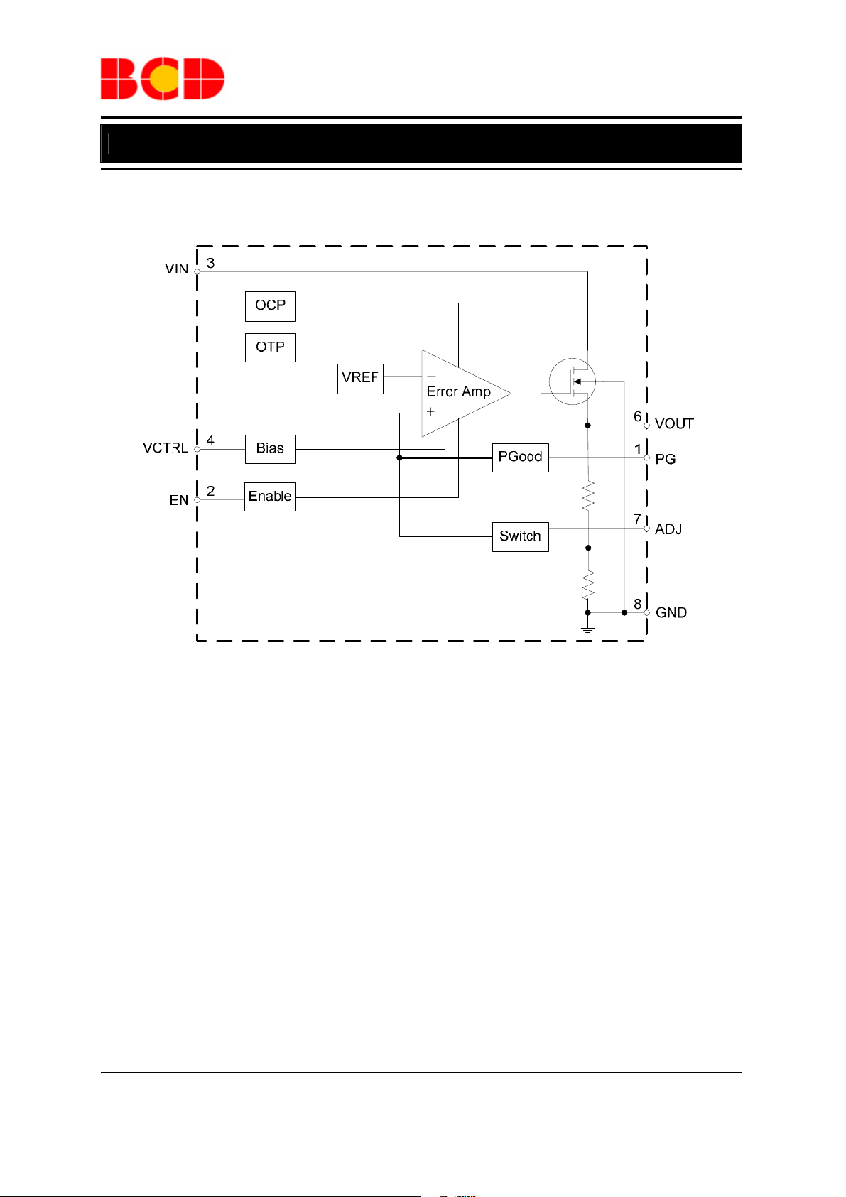
Functional Block Diagram
Figure 3. Functional Block Diagram of AP2132A
Mar. 2012 Rev 1.0 BCD Semiconductor Manufacturing Limited
3

p
Data Sheet
Peak 3A CMOS LDO Regulator with Enable and Power Good AP2132A
Ordering Information
AP2132A -
Circuit Type G1: Green
Package Blank: Tube
MP: PSOP-8
TR: Tape & Reel
1.2: Fixed Output 1.2V
1.5: Fixed Output 1.5V
1.8: Fixed Output 1.8V
2.5: Fixed Out
ut 2.5V
Package
PSOP-8
Temperature
Range
-40ºC to 85ºC
Version
Description
Each fixed
output
version
integrates
ADJ version
Part Number Marking ID
AP2132AMP-1.2G1 2132A-1.2G1 Tube
AP2132AMP-1.2TRG1 2132A-1.2G1
AP2132AMP-1.5G1 2132A-1.5G1 Tube
AP2132AMP-1.5TRG1 2132A-1.5G1
AP2132AMP-1.8G1 2132A-1.8G1 Tube
AP2132AMP-1.8TRG1 2132A-1.8G1
AP2132AMP-2.5G1 2132A-2.5G1 Tube
AP2132AMP-2.5TRG1 2132A-2.5G1
Packing
Type
Tape &
Reel
Tape &
Reel
Tape &
Reel
Tape &
Reel
BCD Semiconductor's Pb-free products, as designated with "G1" suffix in the part number, are RoHS compliant
and Green.
Mar. 2012 Rev 1.0 BCD Semiconductor Manufacturing Limited
4
 Loading...