

Page 1
A
A
f
Description
Product Line o
Diodes Incorporated
P2127
300mA HIGH SPEED, EXTREMELY LOW NOISE CMOS LDO REGULATOR
Features
The AP2127 Series are positive voltage regulator ICs fabricated by
CMOS process.
The AP2127 Series have features of low dropout voltage, low noise,
high output voltage accuracy, and low current consumption which
make them ideal for use in various battery-powered devices.
AP2127 has 1.0V, 1.2V, 1.5V, 1.8V, 2.5V, 2.8V, 3.0V, 3.3V, 4.2V,
4.75V, 5.2V fixed voltage versions and 0.8V to 5.5V adjustable
voltage versions.
AP2127 Series are available in SOT-23 (for fixed versions only),
SOT-23-3 (for fixed versions only), SOT-23-5, SOT-89 (for fixed
versions only) and DFN-2x2-6 packages.
Applications
• Datacom
• Notebook Computers
• Mother Board
Notes: 1. No purposely added lead. Fully EU Directive 2002/95/EC (RoHS) & 2011/65/EU (RoHS 2) compliant.
2. See http://www.diodes.com/quality/lead_free.html for more information about Diodes Incorporated’s definitions of Halogen- and Antimony-free, "Green"
and Lead-free.
3. Halogen- and Antimony-free "Green” products are defined as those which contain <900ppm bromine, <900ppm chlorine (<1500ppm total Br + Cl) and
<1000ppm antimony compounds.
• Wide Operating Voltage: 2.5V to 6V
• High Output Voltage Accuracy: ±2%
• High Ripple Rejection:
68dB @ f = 1kHz, 54dB @ f = 10kHz
• Low Standby Current: 0.1μA
• Low Dropout Voltage: 170mV @ 300mA for V
and C
OUT
OUT
= 5.2V
RMS
@V
OUT
DS(ON)
= 0.8V
= 60Ω
@ 300mA for V
• Low Quiescent Current: 60μA Typical
• Low Output Noise: 60μV
• Short Current Limit: 50mA
• Over Temperature Protection
• Compatible with Low ESR Ceramic Capacitor:
1μF for C
• Excellent Line/Load Regulation
• Soft Start Time: 50μs
• Auto Discharge Resistance: R
• Totally Lead-Free & Fully RoHS Compliant (Notes 1 & 2)
• Halogen and Antimony Free. “Green” Device (Note 3)
IN
= 3.3V, 140mV
OUT
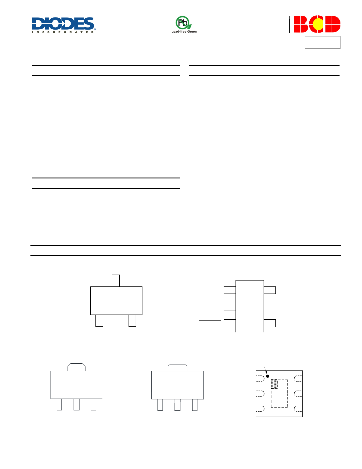
Pin Assignments
(Top View) (Top View)
V
IN
3
1
V
IN
V
5
OUT
GND
2
(SOT-23/SOT-23-3/ N/N3 Package) (SOT-23-5/ K Package)
(Top View) (Top View) (Top View)
1
GND
2
V
OUT
Shutdown
3
P in 1 Mark
1
EN
4
NC/ADJ
123
V
GND
(SOT-89 Option 1/ R Package) (SOT-89 Option 2/ R Package) (DFN-2x2-6/ DN Package)
V
IN
OUT
AP2127
Document number: DS36478 Rev. 3 - 2
1
2
GND
V
www.diodes.com
IN
1 of 27
3
V
OUT
GND
2
34
V
IN
6
5
NC
NC
V
OUT
January 2014
© Diodes Incorporated
Page 2
A
A
f
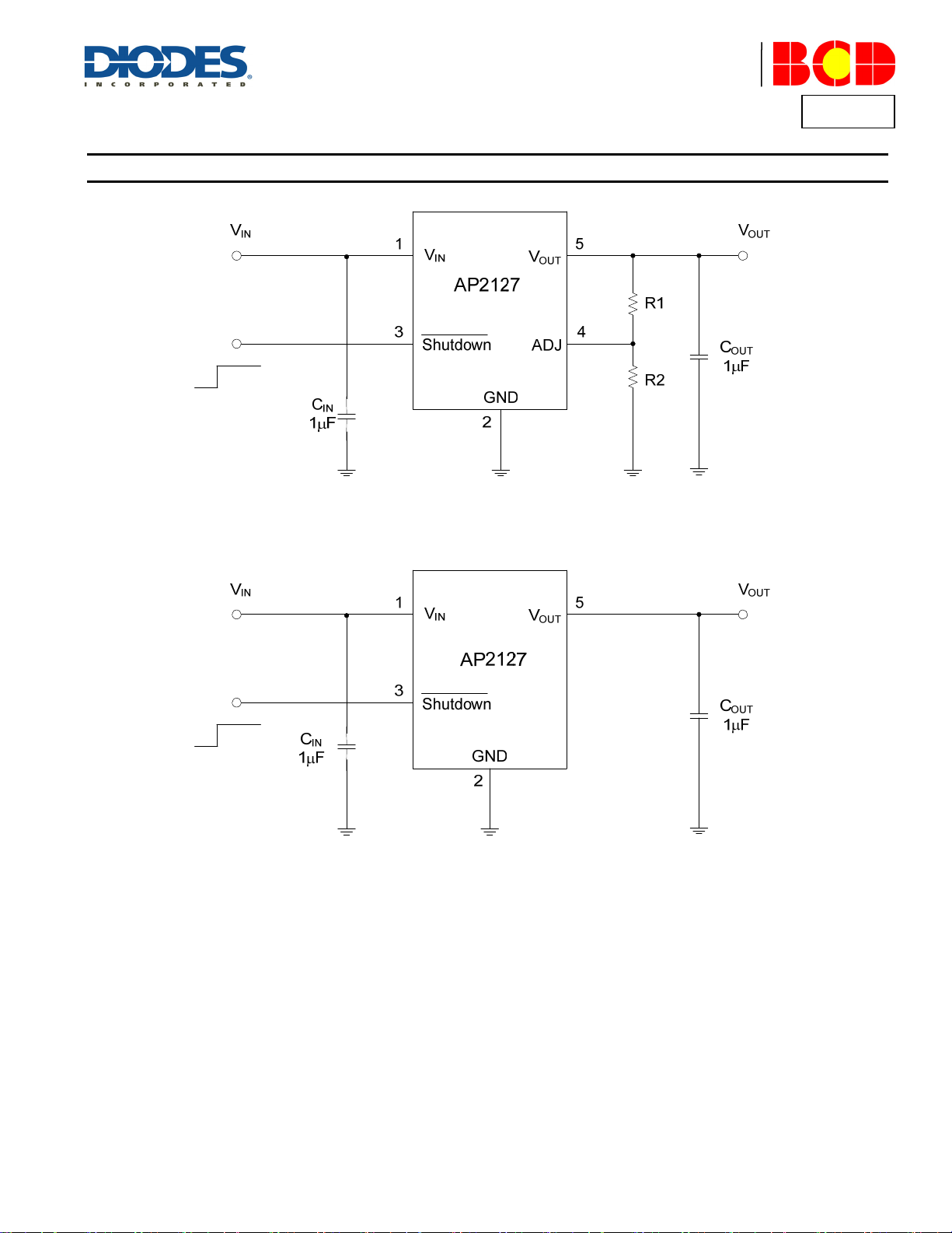
Typical Applications Circuit
Product Line o
Diodes Incorporated
P2127
= 0.8(1+R1/R2)V
V
OUT
For 1.0V to 5.2V Fixed Voltage Versions
AP2127
Document number: DS36478 Rev. 3 - 2
2 of 27
www.diodes.com
January 2014
© Diodes Incorporated
Page 3
A
A
f
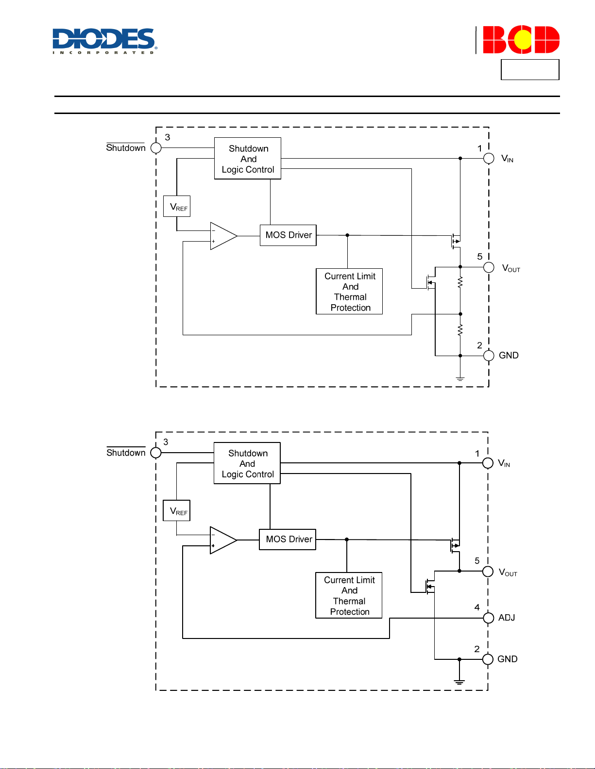
Functional Block Diagram
Product Line o
Diodes Incorporated
P2127
Fixed Version (SOT-23-5 Package)
AP2127
Document number: DS36478 Rev. 3 - 2
Adjustable Version (SOT-23-5 Package)
3 of 27
www.diodes.com
January 2014
© Diodes Incorporated
Page 4
A
A
f
Product Line o
Diodes Incorporated
P2127
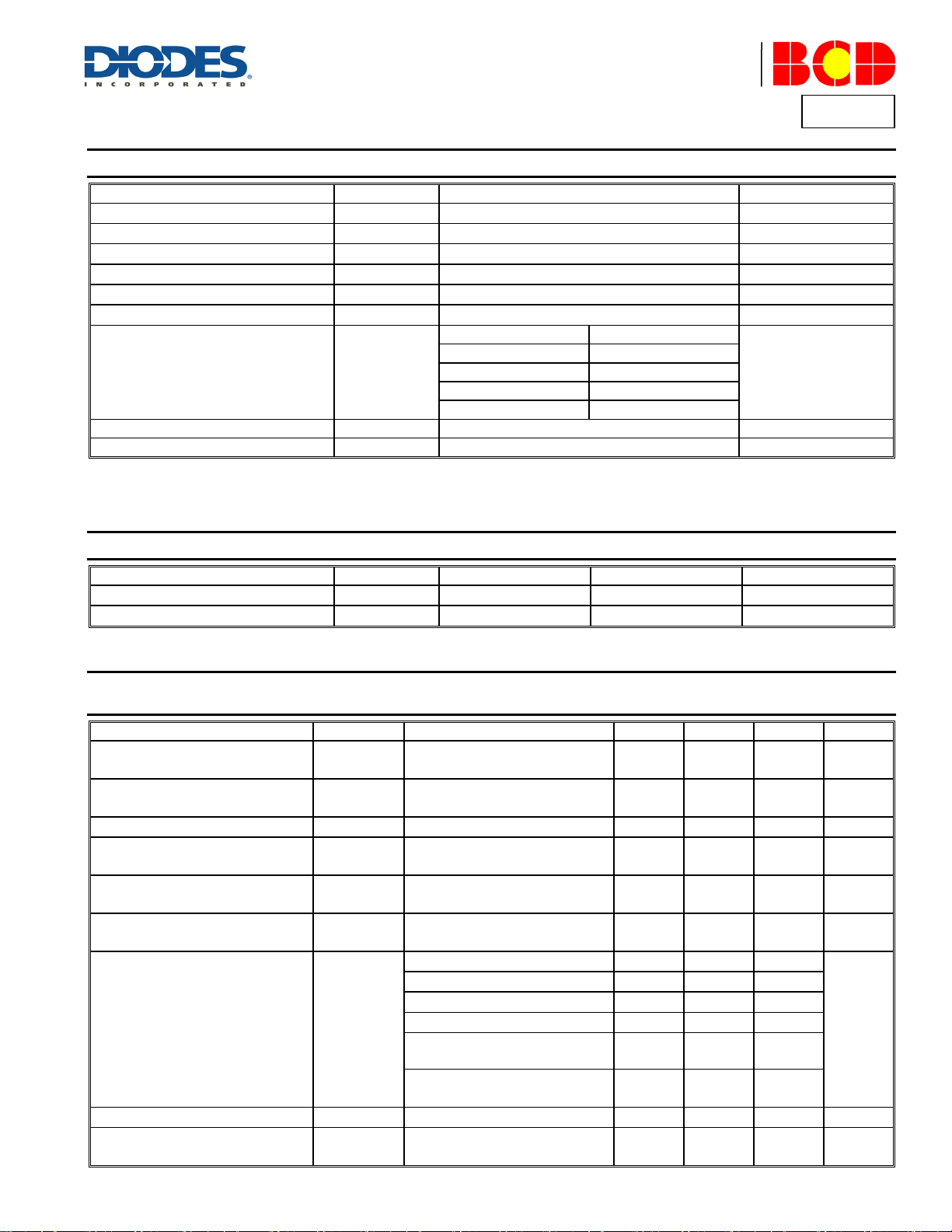
Absolute Maximum Ratings (Note 4) (@T
Parameter Symbol Value Unit
Input Voltage
Shutdown Input Voltage
Output Current
Junction Temperature
Storage Temperature Range
Lead Temperature (Soldering, 10sec)
Thermal Resistance
(Junction to Ambient)
ESD (Human Body Model) ESD 6000 V
ESD (Machine Model) ESD 200 V
Note: 4. Stresses greater than those listed under "Absolute Maximum Ratings" may cause permanent damage to the device. These are stress ratings only, and
functional operation of the device at these or any other conditions beyond those indicated under "Recommended Operating Conditions" is not implied.
Exposure to "Absolute Maximum Ratings" for extended periods may affect device reliability.
Recommended Operating Conditions (@T
Parameter Symbol Min Max Unit
Input Voltage
Operating Ambient Temperature Range
Electrical Characteristics (V
V
= 6V @ V
IN
Reference Voltage
Output Voltage
Input Voltage
Maximum Output Current
Load Regulation
Line Regulation
Dropout Voltage
Quiescent Current IQ
Standby Current I
= 5.2V, TA = +25°C, C
OUT
Parameter Symbol Conditions Min Typ Max Unit
= 2.5V (for 0.8V to 1.8V voltage versions), V
IN
= 1μF, C
IN
V
REF
V
OUT
V
IN
I
OUT(MAX)
∆V
OUT
∆V
OUT
V
DROP
STD
OUT
= +25°C, unless otherwise specified.)
A
V
IN
V
-0.3 to VIN +0.3
CE
I
OUT
T
J
T
STG
T
LEAD
6.5 V
450 mA
+150 °C
-65 to +150 °C
+260 °C
SOT-23 180
SOT-23-3 250
θ
JA
SOT-23-5 250
°C/W
SOT-89 100
DFN-2X2-6 85
= +25°C, unless otherwise specified.)
A
V
IN
T
A
2.5 6 V
-40 +85 °C
= V
IN
+1V (for 2.5V to 4.75V voltage versions),
OUT
= 1μF, Bold typeface applies over -40°C ≤ TA ≤ +85°C unless otherwise specified.)
V
= V
IN
1mA ≤ I
V
IN
1mA ≤ I
–
V
IN
V
OUT
V
IN
1mA ≤ I
V
OUT
I
OUT
V
OUT
V
OUT
V
OUT
V
OUT
V
OUT
4.2V, I
V
OUT
I
OUT
V
IN
V
IN
V
SHUTDOWN
+1V
OUT
≤ 300mA
OUT
= V
+1V
OUT
≤ 300mA
OUT
= V
= 1V
OUT
= 0.98 x V
= V
OUT
OUT
= 1V
OUT
≤ 300mA
+ 0.5V ≤ VIN ≤6V
= 30mA
= 1.0V, I
= 1.2V, I
= 1.5V, I
= 1.8V, I
= 300mA
OUT
= 300mA
OUT
= 300mA
OUT
= 300mA
OUT
= 2.5V, 2.8V, 3.0V, 3.3V,
= 300mA
OUT
= 4.75 and 5.2V,
= 300mA
= V
= V
OUT
OUT
+1V, I
+1V
OUT
= 0mA
in off mode
0.784 0.8 0.816 V
98% x
V
OUT
–
102% x
V
OUT
2.5 – 6 V
300 400 – mA
– 4 10 mV
– 0.5 5 mV
–
–
1400 1500
1200 1300
– 900 1000
–
–
–
140 300
–
–
600 700
170 300
60 90 µA
0.1 1.0 µA
V
V
mV
AP2127
Document number: DS36478 Rev. 3 - 2
4 of 27
www.diodes.com
January 2014
© Diodes Incorporated
Page 5
A
A
f
Product Line o
Diodes Incorporated
P2127
Electrical Characteristics (V
V
= 6V @ V
IN
= 5.2V, TA = +25°C, C
OUT
= 2.5V (for 0.8V to 1.8V voltage versions), V
IN
= 1μF, C
IN
= 1μF, Bold typeface applies over -40°C ≤ TA ≤ +85°C unless otherwise specified.)
OUT
= V
IN
+1V (for 2.5V to 4.75V voltage versions),
OUT
Parameter Symbol Conditions Min Typ Max Unit
f = 100Hz – 68 – dB
f = 1kHz – 68 – dB
f = 10kHz – 54 – dB
f = 100Hz – 63 – dB
f = 1kHz – 63 – dB
P-P
f = 10kHz – 45 – dB
– ±100 – ppm/°C
– 50 – mA
– 60 –
µV
Power Supply Rejection Ration PSRR
Output Voltage Temperature
Coefficient
Short Current Limit
Soft Start Time
RMS Output Noise
∆V
OUT/VOUT
I
SHORT
V
/∆T
t
SS
NOISE
AP2127-1.0V to
4.2V, Ripple 1V
= V
V
IN
OUT
P-P
+1V
AP2127-4.75V and
5.2V, Ripple 0.5V
V
= V
IN
I
OUT
V
OUT
– – 50 – µs
T
A
V
OUT
+1V
OUT
= 30mA, -40°C ≤ TA ≤ +85°C
= 0V
= +25°C, 10Hz ≤ f ≤ 100kHz,
= 0.8V
Shutdown High Voltage – Shutdown Input Voltage High 1.5 – – V
Shutdown Low Voltage – Shutdown Input Voltage Low 0 – – V
V
Discharge MOSFET R
OUT
DS(ON)
– Shutdown Input Voltage Low – 60 – Ω
Shutdown Pull Down Resistance – – – 3 – MΩ
Thermal Shutdown – – – +165 –
Thermal Shutdown Hysteresis – – – +30 –
SOT-23 – 100 –
SOT-23-3 – 150 –
Thermal Resistance
θ
JC
SOT-23-5 – 150 –
SOT-89 – 75 –
DFN-2x2-6 – 60 –
AP2127
Document number: DS36478 Rev. 3 - 2
www.diodes.com
5 of 27
January 2014
© Diodes Incorporated
RMS
°C
°C/W
Page 6
A
A
f
Product Line o
Diodes Incorporated
P2127
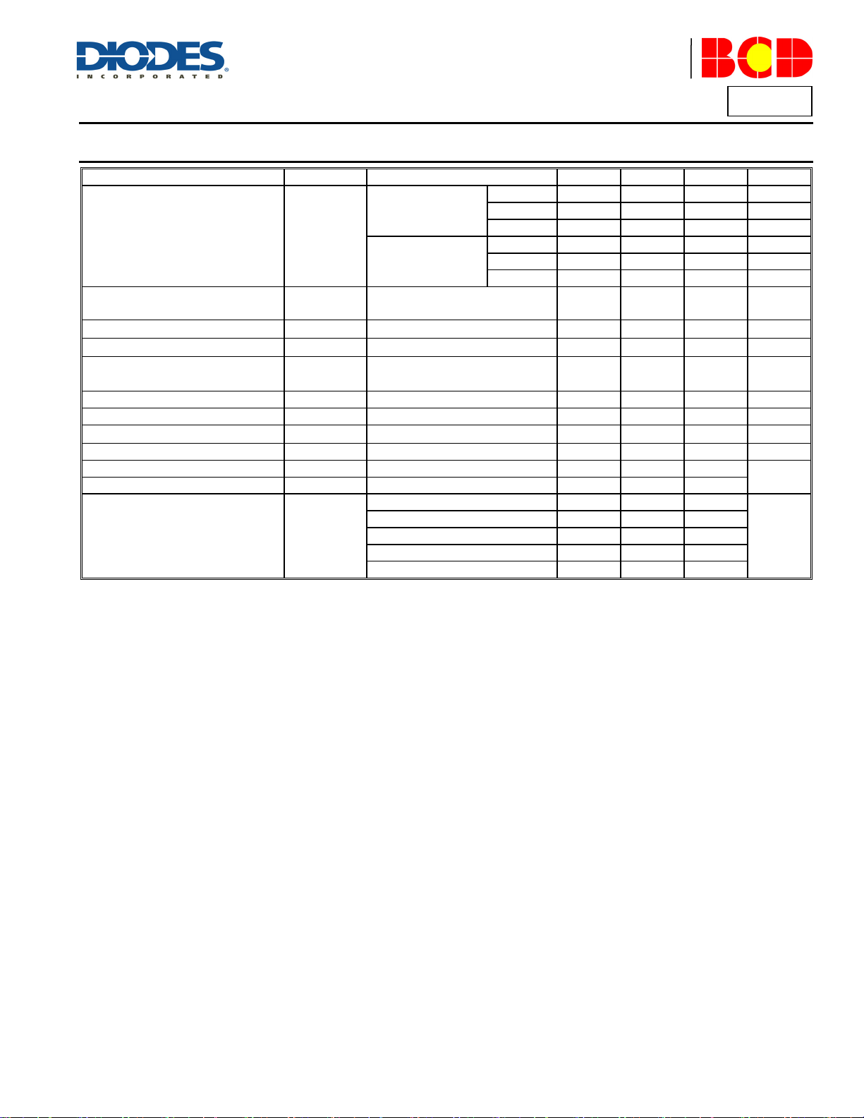
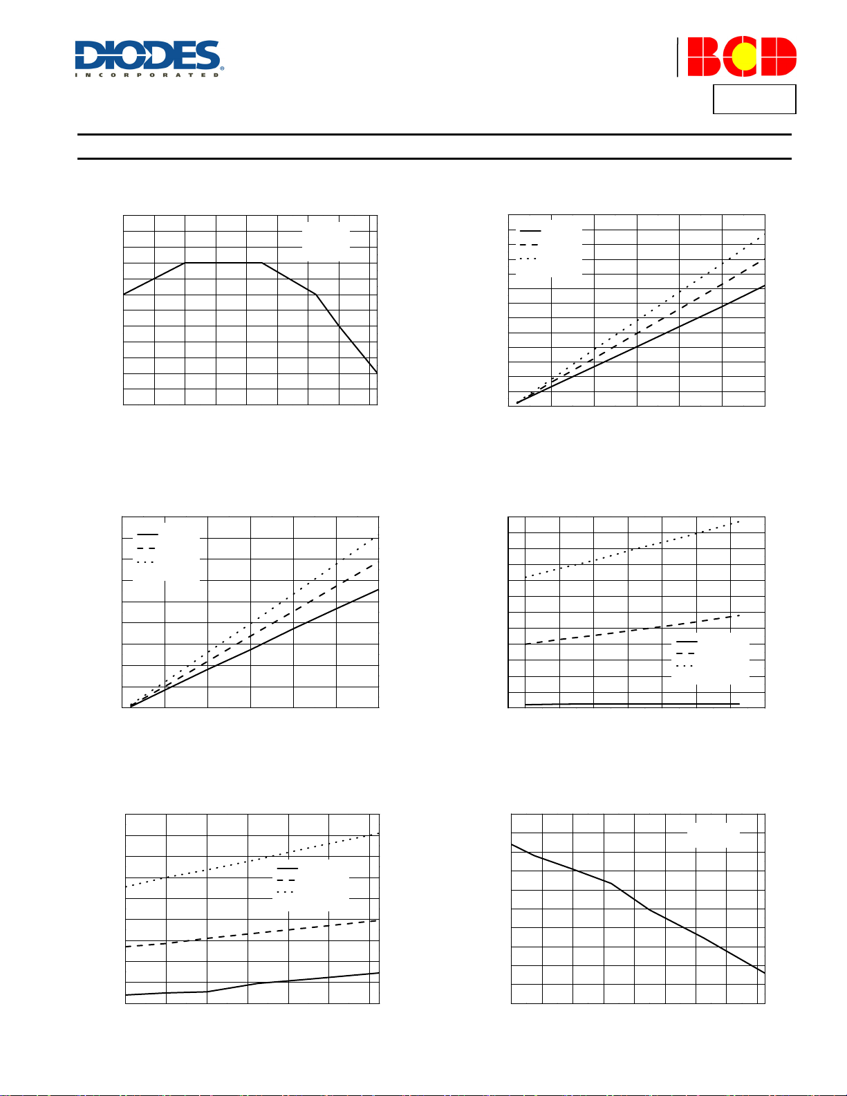
Performance Characteristics
Output Voltage vs. Case Temperature Output Voltage vs. Case Temperature
1.010
1.009
1.008
1.007
1.006
1.005
1.004
1.003
Output Voltage (V)
1.002
1.001
1.000
I
=10mA
OUT
I
=150mA
OUT
I
=300mA
OUT
V
=2.5V
IN
V
=1.0V
OUT
-40-200 20406080100120
Case Temperature (oC)
Output Voltage vs. Case Temperature Output Voltage vs. Input Voltage
5.275
5.270
5.265
5.260
5.255
5.250
5.245
5.240
Output Voltage (V)
5.235
5.230
5.225
I
=10mA
OUT
I
=150mA
OUT
I
=300mA
OUT
V
=6V, V
IN
-40 -20 0 20 40 60 80 100 120
=5.2V
OUT
Case Temperature (oC)
Output Voltage vs. Input Voltage Output Voltage vs. Input Voltage
3.5
3.0
2.5
2.0
1.5
1.0
Output Voltage (V)
0.5
0.0
0.0 0.5 1.0 1.5 2.0 2.5 3.0 3.5 4.0 4.5 5.0 5.5 6.0
Input Voltage (V)
T
=25oC, V
C
I
OUT
I
OUT
=0
=300mA
=3.3V
OUT
3.340
3.338
3.336
3.334
3.332
3.330
Output Voltage (V)
3.328
3.326
3.324
-40 -20 0 20 40 60 80 100 120
Case Temperature (oC)
1.0
0.8
0.6
0.4
Output Voltage (V)
0.2
0.0
0.0 0.5 1.0 1.5 2.0 2.5 3.0 3.5 4.0 4.5 5.0 5.5 6.0
6.0
I
=25oC, V
T
C
OUT
I
OUT
=0
=300mA
=5.2V
OUT
5.5
5.0
4.5
4.0
3.5
3.0
2.5
2.0
Output Voltage (V)
1.5
1.0
0.5
0.0
0123456
Input Voltage (V)
Input Voltage (V)
V
V
=4.3V
IN
OUT
T
V
I
OUT
I
I
=3.3V
=25oC
C
OUT
=10mA
OUT
OUT
I
OUT
I
OUT
=1.0V
=150mA
=300mA
=0
=300mA
AP2127
Document number: DS36478 Rev. 3 - 2
6 of 27
www.diodes.com
January 2014
© Diodes Incorporated
Page 7
A
A
f
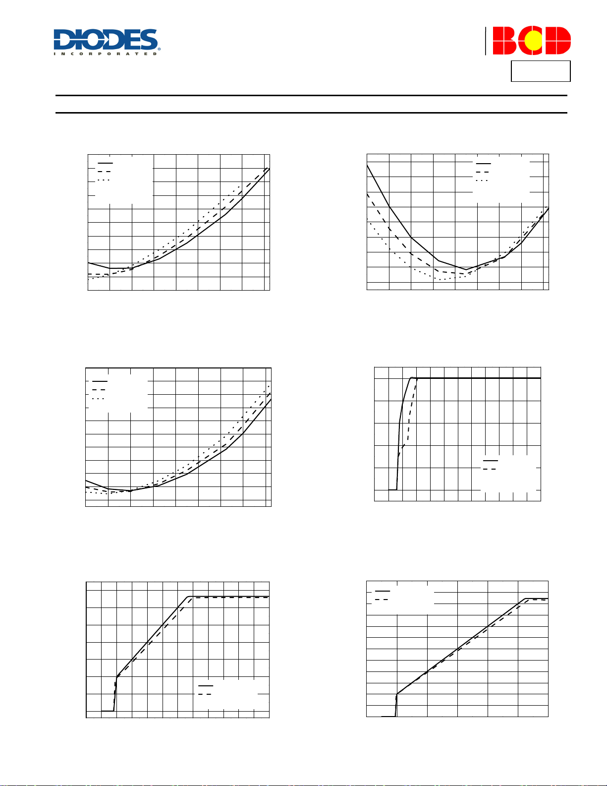
Performance Characteristics (cont.)
Output Voltage vs. Output Current Output Voltage vs. Output Current
1.0
0.8
0.6
0.4
Output Voltage (V)
0.2
0.0
0.00 0.05 0.10 0.15 0.20 0.25 0.30 0.35 0.40 0.45 0.50
Output Voltage vs. Output Current Output Voltage vs. Output Current
3.5
3.0
2.5
2.0
1.5
Output Voltage (V)
1.0
0.5
0.0
VIN=3.8V
VIN=4.3V
VIN=6V
T
=25oC, V
C
0.00 0.05 0.10 0.15 0.20 0.25 0.30 0.35 0.40 0.45 0.50 0.55 0.60
OUT
=3.3V
Quiescent Current vs. Input Voltage Quiescent Current vs. Input Voltage
80
70
60
50
40
30
20
Quiescent Current (μA)
10
0
-10
123456
AP2127
Document number: DS36478 Rev. 3 - 2
Output Current (A)
Output Current (A)
Input Voltage (V)
V
IN
V
OUT
I
OUT
V
OUT
TC=-40oC
TC=25oC
TC=85oC
=2.5V
=1.0V
TC=-40oC
TC=25oC
TC=85oC
=0
=1.0V
7 of 27
www.diodes.com
Product Line o
Diodes Incorporated
P2127
3.5
3.0
2.5
2.0
1.5
V
V
I
IN
=6V, V
IN
OUT
TC=-40oC
TC=25oC
TC=85oC
=4.3V, V
TC=-40oC
TC=25oC
TC=85oC
TC=-40oC
TC=25oC
TC=85oC
=0, V
=3.3V
OUT
=5.2V
OUT
=3.3V
OUT
January 2014
© Diodes Incorporated
Output Voltage (V)
1.0
0.5
0.0
0.00 0.05 0.10 0.15 0.20 0.25 0.30 0.35 0.40 0.45 0.50 0.55 0.60
Output Current (A)
6
5
4
3
2
Output Voltage (V)
1
0
0.0 0.1 0.2 0.3 0.4 0.5
80
70
60
50
40
30
20
Quiescent Current (μA)
10
0
0123456
Output Current (A)
Input Voltage (V)
Page 8
A
A
f
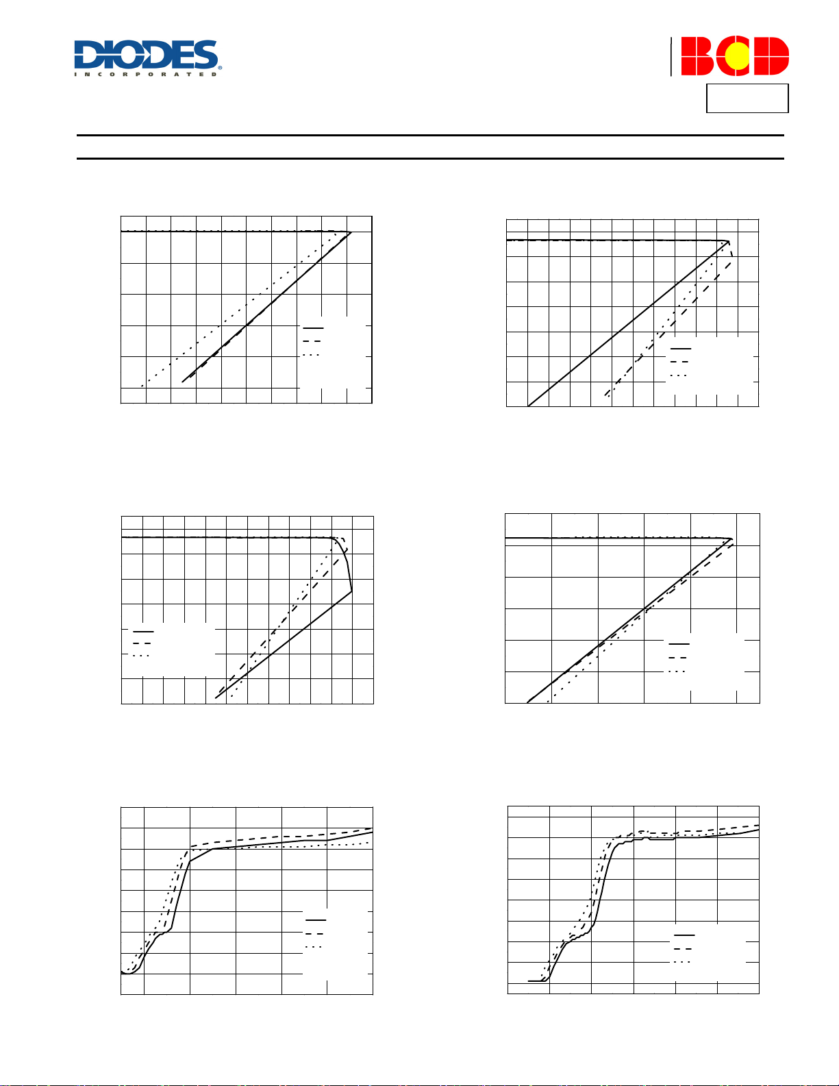
Performance Characteristics (cont.)
Quiescent Current vs. Input Voltage Quiescent Current vs. Output Current
80
70
60
50
40
30
Quiescent Current (μA)
20
10
0
0123456
Input Voltage (V)
I
OUT
TC=-40oC
TC=25oC
TC=85oC
=0, V
OUT
=5.2V
Quiescent Current vs. Output Current Quiescent Current vs. Output Current
115
110
105
100
95
90
85
80
Quiescent Current (μA)
75
70
65
0.00 0.05 0.10 0.15 0.20 0.25 0.30
V
=4.3V, V
IN
TC=-40oC
TC=25oC
TC=85oC
OUT
=3.3V
Quiescent Current vs. Case Temperature Quiescent Current vs. Case Temperature
64
62
60
58
Output Current (A)
VIN=2.5V
=0
I
OUT
V
=1.0V
OUT
56
Quiescent Current (μA)
54
52
-40-20 0 20406080100120
Case Temperature (oC)
Product Line o
Diodes Incorporated
P2127
120
TC=-40oC
110
100
Quiescent Current (μA)
110
105
100
Quiescent Current (μA)
TC=25oC
TC=85oC
V
=2.5V
IN
=1.0V
V
OUT
90
80
70
60
0.00 0.05 0.10 0.15 0.20 0.25 0.30
TC=-40oC
TC=25oC
TC=85oC
V
=6V, V
OUT
=5.2V
IN
95
90
85
80
75
70
0.00 0.05 0.10 0.15 0.20 0.25 0.30
73
72
71
70
69
Quiescent Current (μA)
68
I
=0
OUT
=4.3V
V
IN
=3.3V
V
67
OUT
-40-20 0 20406080100120
Case Temperature (oC)
Output Current (A)
Output Current (A)
AP2127
Document number: DS36478 Rev. 3 - 2
8 of 27
www.diodes.com
January 2014
© Diodes Incorporated
Page 9
A
A
f
Product Line o
Diodes Incorporated
Performance Characteristics (cont.)
Quiescent Current vs. Case Temperature Dropout Voltage vs. Output Current
80
79
78
77
76
75
74
73
72
71
Quiescent Current (μA)
70
69
68
-40-20 0 20406080100120
Case Temperature (oC)
I
=0
OUT
=6V
V
IN
V
=5.2V
OUT
0.26
0.24
0.22
0.20
0.18
0.16
0.14
0.12
0.10
0.08
Dropout Voltage (V)
0.06
0.04
0.02
0.00
TC=-40oC
TC=25oC
TC=85oC
V
=3.3V
OUT
0.00 0.05 0.10 0.15 0.2 0 0.25 0.30
Dropout Voltage vs. Output Current Dropout Voltage vs. Case Temperature
0.18
0.16
0.14
0.12
0.10
0.08
0.06
Dropout Voltage (V)
0.04
0.02
0.00
0.00 0.05 0.10 0.15 0.2 0 0.25 0.30
V
OUT
TC=-40oC
TC=25oC
TC=85oC
=5.2V
Dropout Voltage vs. Case Temperature Power Dissipation vs. Case Temperature
0.18
0.16
0.14
0.12
0.10
0.08
0.06
Dropout Voltage (V)
0.04
0.02
0.00
-40-20 0 20406080
Case Temperature (oC)
AP2127
Document number: DS36478 Rev. 3 - 2
Output Current (A)
0.24
0.22
0.20
0.18
0.16
0.14
I
=10mA
OUT
I
=150mA
OUT
I
=300mA
OUT
=5.2V
V
OUT
0.12
0.10
0.08
Dropout Voltage (V)
0.06
0.04
0.02
0.00
-40 -20 0 20 40 60 80 100
Case Temperature (oC)
2.0
1.8
1.6
1.4
1.2
1.0
0.8
0.6
Power Dissipation (W)
0.4
0.2
0.0
-40 -20 0 20 40 60 80 100 120
Case Temperature (oC)
9 of 27
www.diodes.com
Output Current (A)
I
I
I
=3.3V
V
OUT
V
OUT
No heatsink
OUT
OUT
OUT
=1.0V
=10mA
=150mA
=300mA
© Diodes Incorporated
P2127
January 2014
Page 10

A
A
f
Performance Characteristics (cont.)
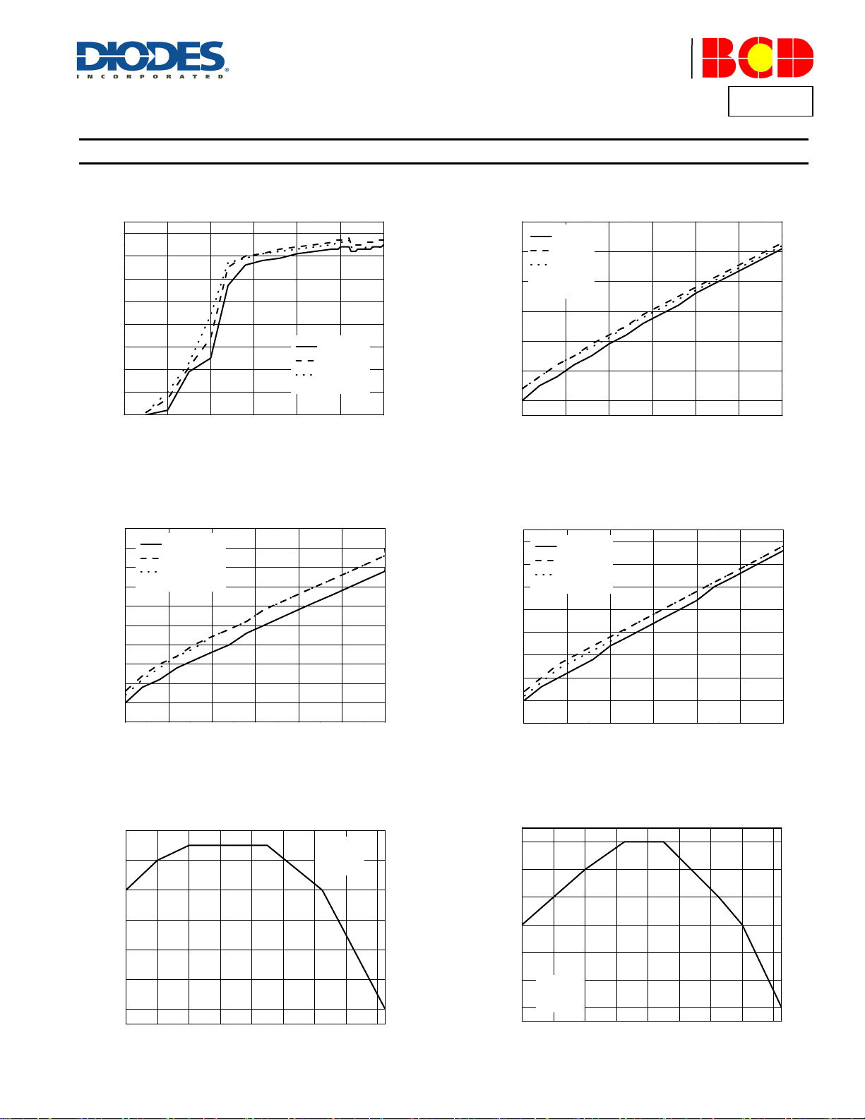
Line Transient Load Transient
(Condition: C
V
IN
IN=COUT
=2.5V to 3.3V, V
VIN
500mV/div
V
OUT
50mV/div
Load Transient Load Transient
(Condition: C
V
IN=COUT
=4.3V, V
IN
200mA/div
I
OUT
V
OUT
50mV/div
PSRR vs. Frequency PSRR vs. Frequency
(Condition: C
IN=COUT
Ripple=1V
90
80
70
60
50
40
PSRR (dB)
30
20
10
0
100 1000 10000 100000
AP2127
Document number: DS36478 Rev. 3 - 2
=1µF, I
OUT
=1µF, I
=10mA to 300mA, (Condition: CIN=C
OUT
=3.3V) VIN=6V, V
OUT
=1µF, VIN=2.5V, V
) Ripple=1VPP)
PP
I
OUT
I
OUT
V
=1V,Ripple=1V
OUT
Frequency (Hz)
=10mA, (Condition: CIN=C
OUT
=1V) VIN=2.5V, V
=10mA
=300mA
Product Line o
Diodes Incorporated
I
OUT
200mA/div
50mV/div
200mA/div
50mV/div
=1V (Condition: CIN=C
OUT
PP
10 of 27
www.diodes.com
V
OUT
I
OUT
V
OUT
70
60
50
40
PSRR (dB)
30
20
V
10
I
OUT
I
OUT
=3.3V, Ripple=1V
OUT
100 1k 10k 100k
OUT
=10mA
=300mA
=1µF, Slew Rate=20mA/µs,
OUT
=1V, I
OUT
OUT
=5.2V, I
OUT
PP
Frequency (Hz)
=10mA to 300mA)
OUT
=1µF, Slew Rate=20mA/µs,
=10mA to 300mA)
OUT
=1µF, VIN=4.3V, V
© Diodes Incorporated
P2127
=3.3V,
OUT
January 2014
Page 11

A
A
f
Performance Characteristics (Cont.)
PSRR vs. Frequency Region of Stable C
(Condition: C
Ripple=0.5V
70
60
50
40
PSRR (dB)
30
I
20
10
=10mA
OUT
I
=300mA
OUT
V
=5.2V, Ripple=0.5V
OUT
100 1k 10k 100k
Region of Stable C
Output Current (C
AP2127
Document number: DS36478 Rev. 3 - 2
IN=COUT
PP
Frequency (Hz)
=1µF, VIN=6V, V
)
PP
ESR vs.
OUT
= 4.7µF)
OUT
OUT
Product Line o
Diodes Incorporated
=5.2V, Output Current (C
11 of 27
www.diodes.com
ESR vs.
OUT
= 1µF)
OUT
P2127
January 2014
© Diodes Incorporated
Page 12

A
A
f
Product Line o
Diodes Incorporated
P2127
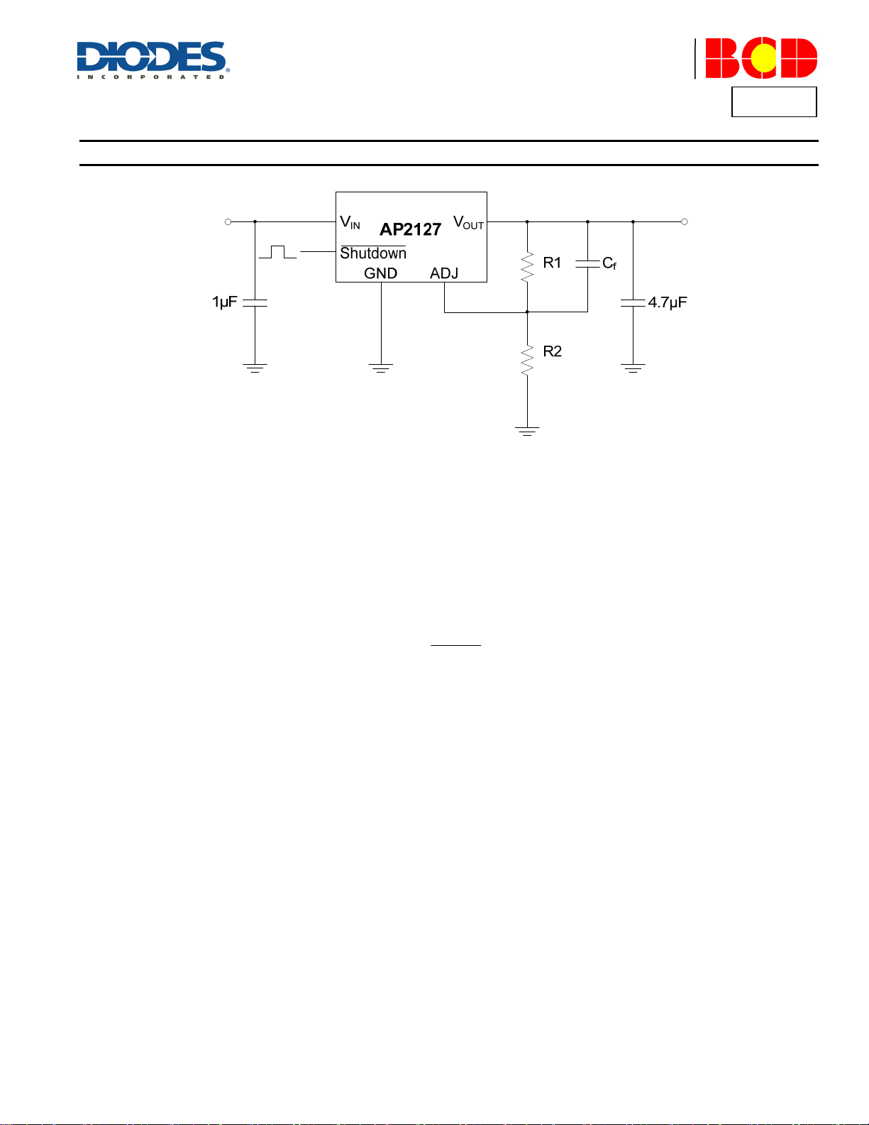
Application Notes
Input Capacitor
A 1µF ceramic capacitor is recommended to connect between VIN and GND pins to decouple input power supply glitch and noise. The amount of
the capacitance may be increased without limit. This input capacitor must be located as close as possible to the device to assure input stability
and less noise. For PCB layout, a wide copper trace is required for both V
and GND.
IN
Output Capacitor
The output capacitor is required to stabilize and help transient response for LDO. The AP2127 is stable with very small ceramic output capacitor
with a low ESR 1µF or higher of X7R or X5R MLCC capacitor, which will be sufficient at full temperature ranges. Additional capacitance helps to
reduce undershoot and overshoot during transient. Place output capacitor as close as possible to V
as possible.
and GND pins, and keep the leads as short
OUT
Adjustable Operation
For adjustable version, the output voltage is calculated by:
⎛
⎜
REFOUT
⎜
⎝
Where V
Rearranging the equation will give the following that is used for adjusting the output to a particular voltage:
For AP2127, the resistor at the low side (R
In order to improve the stability and to decrease the noise level of the adjustable version, a feed-forward capacitor is suggested to be placed
between V
The recommended value of the feed-forward capacitor for different resistor divider ratios is shown in the table below.
= 0.8V (the internal reference voltage)
REF
⎛
V
OUT
⎜
RR
21
⎜
V
REF
⎝
) can be selected from 5kΩ to 200kΩ.
2
and ADJ pins (Figure 1). It’s recommended that this feed-forward capacitor value can be calculated as:
OUT
0.7kHz ≤
Output Voltage R1 R2
1.2V 7.5kΩ 15kΩ 2.7nF
1.6V 7.5kΩ 7.5kΩ 2.7nF
1.8V 22.5kΩ 18kΩ 1nF
1.9V 7.5kΩ 5.49kΩ 2.7nF
2.5V 38.3kΩ 18kΩ 560pF
3.3V 56.2kΩ 18kΩ 390pF
4.0V 120kΩ 30.1kΩ 180pF
Table 1 Output Voltage Setting Guide
1
≤
R2π
××
⎞
R
1
⎟
+=
1VV
⎟
R
2
⎠
⎞
⎟
−= 1
⎟
⎠
15kHz
ffC1
C
ff
AP2127
Document number: DS36478 Rev. 3 - 2
12 of 27
www.diodes.com
January 2014
© Diodes Incorporated
Page 13
A
A
f
Application Notes (cont.)
Product Line o
Diodes Incorporated
P2127
Figure 1. Application Circuit with Feed-forward Capacitor
Current Limit Protection
When output current at V
prevent over-current and to protect the regulator and load from damaged due to overheating.
Short Circuit Protection
When V
pin is shorted to GND, short circuit protection will be triggered and clamp the output current to approximately 50mA.
OUT
Auto discharge with Shutdown Version
For shutdown version, an auto discharge MOSFET with R
charge of the output capacitors quickly when turning off AP2127 with Shutdown pin.
Thermal Consideration
Internal thermal protection circuitry of AP2127 is used to protect device during overload conditions. For continuous operation, ensure not to
exceed the operating junction temperature range of +125°C.
The power dissipation definition in the device is:
= (VIN - V
P
D
The maximum power dissipation depends on the thermal resistance of IC package, PCB layout and the surrounding airflow. The maximum power
dissipation can also be calculated as:
= (T
P
D(MAX)
The maximum power dissipation for SOT-23-5 package (least copper size) at T
= (125°C - 25°C) / (250°C/W) = 0.4W
P
D(MAX)
OUT
J(MAX)
) x I
OUT
- TA) / θ
pin is higher than current limit threshold, the current limit protection will be triggered and clamp the output current to
OUT
+ VIN x I
JA
of 60Ω typical is integrated between V
DS(ON)
Q
= +25°C can be calculated as:
A
and GND pins, which can discharge the
OUT
AP2127
Document number: DS36478 Rev. 3 - 2
2 of 27
www.diodes.com
January 2014
© Diodes Incorporated
Page 14

A
A
f
Ordering Information
Product Line o
Diodes Incorporated
P2127
AP2127 XX -XXXX XX
Product Name
Package
N : SOT-23
N3 : SOT-23-3
K : SOT-23-5
R : SOT-89
DN : DFN-2x2-6
Output Voltage
ADJ : Adjustable Output
1.0 : Fixed Output 1.0V
1.2 : Fixed Output 1.2V
1.5 : Fixed Output 1.5V
1.8 : Fixed Output 1.8V
Packing
TR : Tape & Reel
RoHS/Green
G1 : Green
2.5 : Fixed Output 2.5V
2.8 : Fixed Output 2.8V
3.0 : Fixed Output 3.0V
3.3 : Fixed Output 3.3V
4.2 : Fixed Output 4.2V
4.75 : Fixed Output 4.75V
5.2 : Fixed Output 5.2V
Part Number Marking ID Temperature Range Package Package
AP2127N-1.0TRG1 GU8
AP2127N-1.2TRG1 GS8 3000/Tape & Reel
AP2127N-1.5TRG1 GV8 3000/Tape & Reel
AP2127N-1.8TRG1 GW8 3000/Tape & Reel
AP2127N-2.5TRG1 GT9 3000/Tape & Reel
AP2127N-2.8TRG1 GU9 3000/Tape & Reel
AP2127N-3.0TRG1 GV9 3000/Tape & Reel
AP2127N-3.3TRG1 GW9 3000/Tape & Reel
AP2127N-4.2TRG1 GS9 3000/Tape & Reel
AP2127N-4.75TRG1 GV7 3000/Tape & Reel
AP2127N-5.2TRG1 GW7 3000/Tape & Reel
AP2127N3-1.0TRG1 GU1
AP2127N3-1.2TRG1 GU2 3000/Tape & Reel
AP2127N3-1.5TRG1 GU3 3000/Tape & Reel
AP2127N3-1.8TRG1 GU4 3000/Tape & Reel
AP2127N3-2.5TRG1 GU5 3000/Tape & Reel
AP2127N3-2.8TRG1 GV1 3000/Tape & Reel
AP2127N3-3.0TRG1 GV2 3000/Tape & Reel
AP2127N3-3.3TRG1 GV3 3000/Tape & Reel
AP2127N3-4.2TRG1 GV4 3000/Tape & Reel
AP2127N3-4.75TRG1 GV5 3000/Tape & Reel
AP2127N3-5.2TRG1 GW1 3000/Tape & Reel
AP2127K-ADJTRG1 GEH
AP2127K-1.0TRG1 GEG 3000/Tape & Reel
AP2127K-1.5TRG1 GEP 3000/Tape & Reel
AP2127K-1.8TRG1 GEQ 3000/Tape & Reel
AP2127K-2.5TRG1 GER 3000/Tape & Reel
AP2127K-2.8TRG1 GES 3000/Tape & Reel
AP2127K-3.0TRG1 GHF 3000/Tape & Reel
AP2127K-3.3TRG1 GET 3000/Tape & Reel
AP2127K-4.2TRG1 GEU 3000/Tape & Reel
AP2127K-4.75TRG1 GEZ 3000/Tape & Reel
AP2127K-5.2TRG1 GEW 3000/Tape & Reel
AP2127
Document number: DS36478 Rev. 3 - 2
-40°C to +85°C
14 of 27
www.diodes.com
SOT-23
SOT-23-3
SOT-23-5
3000/Tape & Reel
3000/Tape & Reel
3000/Tape & Reel
January 2014
© Diodes Incorporated
Page 15

A
A
f
Product Line o
Diodes Incorporated
Ordering Information (cont.)
Part Number Marking ID Temperature Range Package Package
AP2127R-1.0TRG1 G22P
AP2127R-1.2TRG1 G27P 1000/Tape & Reel
AP2127R-1.5TRG1 G28P 1000/Tape & Reel
AP2127R-1.8TRG1 G31P 1000/Tape & Reel
AP2127R-2.5TRG1 G33P 1000/Tape & Reel
AP2127R-2.8TRG1 G37P 1000/Tape & Reel
AP2127R-3.0TRG1 G41P 1000/Tape & Reel
AP2127R-3.3TRG1 G42P 1000/Tape & Reel
AP2127R-4.2TRG1 G43P 1000/Tape & Reel
AP2127R-4.75TRG1 G70P 1000/Tape & Reel
AP2127R-5.2TRG1 G78P 1000/Tape & Reel
AP2127DN-ADJTRG1 BV
AP2127DN-1.0TRG1 CA 3000/Tape & Reel
AP2127DN-1.2TRG1 CB 3000/Tape & Reel
AP2127DN-1.5TRG1 CC 3000/Tape & Reel
AP2127DN-1.8TRG1 CD 3000/Tape & Reel
AP2127DN-2.5TRG1 BP 3000/Tape & Reel
AP2127DN-2.8TRG1 BS 3000/Tape & Reel
AP2127DN-3.0TRG1 BU 3000/Tape & Reel
AP2127DN-3.3TRG1 CE 3000/Tape & Reel
AP2127DN-4.2TRG1 CF 3000/Tape & Reel
AP2127DN-4.75TRG1 CG 3000/Tape & Reel
AP2127DN-5.2TRG1 CH 3000/Tape & Reel
-40°C to +85°C
SOT-89
DFN-2x2-6
AP2127
Document number: DS36478 Rev. 3 - 2
15 of 27
www.diodes.com
1000/Tape & Reel
3000/Tape & Reel
January 2014
© Diodes Incorporated
P2127
Page 16

A
A
f
Marking Information
(1) SOT-23, SOT-23-3
(2) SOT-23-5
(3) SOT-89
(4) DFN-2x2-6
AP2127
Document number: DS36478 Rev. 3 - 2
YWWAXX
(Top View)
XXX
(Top View)
XXX
(Top View)
XXXX
(Top View)
XX
Product Line o
Diodes Incorporated
: Logo
XXX: Marking ID (See Ordering Information)
: Logo
XXX: Marking ID (See Ordering Information)
First Line: Logo and Marking ID (See Ordering Information)
Second Line: Date Code
Y: Year
WW: Work Week of Molding
A: Assembly House Code
XX: 7th and 8th Digits of Batch Number
XX: Marking ID (See Ordering Information)
16 of 27
www.diodes.com
© Diodes Incorporated
P2127
January 2014
Page 17

A
A
f
Package Outline Dimensions (All dimensions in mm.)
(1) Package Type: SOT-23
Product Line o
Diodes Incorporated
P2127
AP2127
Document number: DS36478 Rev. 3 - 2
17 of 27
www.diodes.com
January 2014
© Diodes Incorporated
Page 18

A
A
f
Package Outline Dimensions (cont.) (All dimensions in mm.)
(2) Package Type: SOT-23-3
Product Line o
Diodes Incorporated
P2127
°
°
AP2127
Document number: DS36478 Rev. 3 - 2
18 of 27
www.diodes.com
January 2014
© Diodes Incorporated
Page 19

A
A
f
Package Outline Dimensions (cont.) (All dimensions in mm.)
(3) Package Type: SOT-23-5
Product Line o
Diodes Incorporated
P2127
AP2127
Document number: DS36478 Rev. 3 - 2
19 of 27
www.diodes.com
January 2014
© Diodes Incorporated
Page 20

A
A
f
Package Outline Dimensions (cont.) (All dimensions in mm.)
(4) Package Type: SOT-89
Product Line o
Diodes Incorporated
P2127
AP2127
Document number: DS36478 Rev. 3 - 2
20 of 27
www.diodes.com
January 2014
© Diodes Incorporated
Page 21

A
A
f
Package Outline Dimensions (cont.) (All dimensions in mm.)
(5) Package Type: DFN-2x2-6
Product Line o
Diodes Incorporated
P2127
AP2127
Document number: DS36478 Rev. 3 - 2
21 of 27
www.diodes.com
January 2014
© Diodes Incorporated
Page 22

A
A
f
Suggested Pad Layout (All dimensions in mm.)
(1) Package Type: SOT-23
Product Line o
Diodes Incorporated
P2127
Dimensions
Value 2.900/0.114 1.100/0.043 0.800/0.031 0.900/0.035 0.950/0.037
Z
(mm)/(inch)
G
(mm)/(inch)
(mm)/(inch)
X
Y
(mm)/(inch)
E
(mm)/(inch)
AP2127
Document number: DS36478 Rev. 3 - 2
22 of 27
www.diodes.com
January 2014
© Diodes Incorporated
Page 23

A
A
f
Suggested Pad Layout (cont.) (All dimensions in mm.)
(2) Package Type: SOT-23-3
Product Line o
Diodes Incorporated
P2127
Dimensions
Value 3.600/0.142 1.600/0.063 0.700/0.028 1.000/0.039 0.950/0.037 1.900/0.075
(mm)/(inch) G (mm)/(inch) X (mm)/(inch) Y (mm)/(inch)
AP2127
Document number: DS36478 Rev. 3 - 2
Z
23 of 27
www.diodes.com
E1
(mm)/(inch)
E2
(mm)/(inch)
January 2014
© Diodes Incorporated
Page 24

A
A
f
Suggested Pad Layout (cont.) (All dimensions in mm.)
(3) Package Type: SOT-23-5
Product Line o
Diodes Incorporated
P2127
Dimensions
Value 3.600/0.142 1.600/0.063 0.700/0.028 1.000/0.039 0.950/0.037 1.900/0.075
Z
(mm)/(inch) G (mm)/(inch) X (mm)/(inch) Y (mm)/(inch)
E1
(mm)/(inch)
E2
(mm)/(inch)
AP2127
Document number: DS36478 Rev. 3 - 2
24 of 27
www.diodes.com
January 2014
© Diodes Incorporated
Page 25

A
A
f
Suggested Pad Layout (cont.) (All dimensions in mm.)
(4) Package Type: SOT-89
Product Line o
Diodes Incorporated
P2127
Dimensions
Value 4.600/0.181 0.550/0.022 1.850/0.073 0.800/0.031 1.300/0.051 1.475/0.058 1.500/0.059
Z
(mm)/(inch) X (mm)/(inch)
AP2127
Document number: DS36478 Rev. 3 - 2
X1
(mm)/(inch)
25 of 27
www.diodes.com
X2
(mm)/(inch) Y (mm)/(inch)
Y1
(mm)/(inch) E (mm)/(inch)
January 2014
© Diodes Incorporated
Page 26

A
A
f
Suggested Pad Layout (cont.) (All dimensions in mm.)
(5) Package Type: DFN-2x2-6
Product Line o
Diodes Incorporated
P2127
Dimensions
Value 2.400/0.094 0.300/0.012 0.500/0.020 1.600/0.063 1.000/0.039
Y
(mm)/(inch)
X1
(mm)/(inch)
Y1=E
(mm)/(inch)
X2
(mm)/(inch)
Y2
(mm)/(inch)
AP2127
Document number: DS36478 Rev. 3 - 2
26 of 27
www.diodes.com
January 2014
© Diodes Incorporated
Page 27

A
A
f
Product Line o
Diodes Incorporated
P2127
DIODES INCORPORATED MAKES NO WARRANTY OF ANY KIND, EXPRESS OR IMPLIED, WITH REGARDS TO THIS DOCUMENT,
INCLUDING, BUT NOT LIMITED TO, THE IMPLIED WARRANTIES OF MERCHANTABILITY AND FITNESS FOR A PARTICULAR PURPOSE
(AND THEIR EQUIVALENTS UNDER THE LAWS OF ANY JURISDICTION).
Diodes Incorporated and its subsidiaries reserve the right to make modifications, enhancements, improvements, corrections or other changes
without further notice to this document and any product described herein. Diodes Incorporated does not assume any liability arising out of the
application or use of this document or any product described herein; neither does Diodes Incorporated convey any license under its patent or
trademark rights, nor the rights of others. Any Customer or user of this document or products described herein in such applications shall assume
all risks of such use and will agree to hold Diodes Incorporated and all the companies whose products are represented on Diodes Incorporated
website, harmless against all damages.
Diodes Incorporated does not warrant or accept any liability whatsoever in respect of any products purchased through unauthorized sales channel.
Should Customers purchase or use Diodes Incorporated products for any unintended or unauthorized application, Customers shall indemnify and
hold Diodes Incorporated and its representatives harmless against all claims, damages, expenses, and attorney fees arising out of, directly or
indirectly, any claim of personal injury or death associated with such unintended or unauthorized application.
Products described herein may be covered by one or more United States, international or foreign patents pending. Product names and markings
noted herein may also be covered by one or more United States, international or foreign trademarks.
This document is written in English but may be translated into multiple languages for reference. Only the English version of this document is the
final and determinative format released by Diodes Incorporated.
Diodes Incorporated products are specifically not authorized for use as critical components in life support devices or systems without the express
written approval of the Chief Executive Officer of Diodes Incorporated. As used herein:
A. Life support devices or systems are devices or systems which:
1. are intended to implant into the body, or
2. support or sustain life and whose failure to perform when properly used in accordance with instructions for use provided in the
labeling can be reasonably expected to result in significant injury to the user.
B. A critical component is any component in a life support device or system whose failure to perform can be reasonably expected to cause the
failure of the life support device or to affect its safety or effectiveness.
Customers represent that they have all necessary expertise in the safety and regulatory ramifications of their life support devices or systems, and
acknowledge and agree that they are solely responsible for all legal, regulatory and safety-related requirements concerning their products and any
use of Diodes Incorporated products in such safety-critical, life support devices or systems, notwithstanding any devices- or systems-related
information or support that may be provided by Diodes Incorporated. Further, Customers must fully indemnify Diodes Incorporated and its
representatives against any damages arising out of the use of Diodes Incorporated products in such safety-critical, life support devices or systems.
Copyright © 2014, Diodes Incorporated
www.diodes.com
IMPORTANT NOTICE
LIFE SUPPORT
AP2127
Document number: DS36478 Rev. 3 - 2
27 of 27
www.diodes.com
January 2014
© Diodes Incorporated
 Loading...