Hi-Fi Personal Component System
SERVICE MANUAL
For U.S. & Canada model
MODEL
D-107
PERSONAL AUDIO SYSTEM
Some illustrations using in this service manual are slightly different from the actual set.
16-11, YUSHIMA 3-CHOME, BUNKYOU-KU, TOKYO 113-0034 JAPAN
Telephone: 03 (3837) 5321
X0133 205 NC 0112

SAFETY PRECAUTIONS
The following check should be performed for the continued protection of the customer and service technician.
LEAKAGE CURRENT CHECK
Before returning the unit to the customer, make sure you make either (1) a leakage current check or (2) a line to chassis
resistance check. If the leakage current exceeds 0.5 milliamps, or if the resistance from chassis to either side of the
power cord is less than 460 kohms, the unit is defective.
SPECIFICATIONS
Amplifier Section
Practical maximum output: Satellite: 25W + 25W (6Ω/ohms, 1kHz, T.H.D. 0.9%)
Receiver Section
Audio input/output jacks: AUX input/output jacks, Optical digital out jacks
Receive frequency bands: FM: 87.50MHz to 108.00MHz
Receive sensitivity: FM: 1.5µV/75Ω/ohms
FM stereo separation: 35 dB (1 kHz)
Subwoofer: 50W (12Ω/ohms, 100Hz, T.H.D. 0.9%)
AM: 520kHz to 1710kHz
AM: 20µV
D-107
CD Section
Wow and flutter: Below measurement limits (±0.001% W peak)
Sampling frequency: 44.1kHz
Light source: Semiconductor laser
Clock and Timer Section
Clock: Crystal oscillation synchronizing system
Timers: Everyday timer (1 setting)
Common Section
Power supply: 80W
Power consumption: (In the standby mode: 1.5W or less when the eco-mode is set, 20W normally)
Maximum external dimensions: D107: 204 (W) × 293 (H) × 157 (D) mm (Including stand)
Mass: D-107: 2.6kg (5lbs 11.7oz)
(Within one minute per month)
Once timer (1 setting)
Sleep timer (maximum 60 min.)
(8-1/32″ × 11-17/32″ × 6-3/16″)
* With stand removed 204 (W) × 267 (H) × 82 (D) mm
(8-1/32″ × 10-33/64″ × 3-15/64″)
USC-107: 162 (W) × 293 (H) × 149 (D) mm (Including stand)
(6-3/8″ × 11-17/32″ × 5-55/64″)
* With stand removed 162 (W) × 267 (H) × 72 (D) mm
(6-3/8″ × 10-33/64″ × 2-53/64″)
USW-107: 447 (W) × 210 (H) × 205 (D) mm (Including net)
(17-19/32″ × 8-17/64″ × 8-5/64″)
USC-107: 1.4kg (3lbs 1.74oz) (each)
USW-107: 7.9kg (17lbs 6.7oz)
Remote Control (RC-909)
Remote control system: Infrared pulse
Power supply: 3V DC (using two R03/AAA type batteries)
Maximum external dimensions: 48 (W) × 210 (H) × 29 (D) mm
(1-57/64″ × 8-17/64″ × 1-9/64″)
Mass: 120g (4.2oz) (including batteries)
* For improvement purposes, specifications and functions are subject to change without advanced notice.
2
DISASSEMBLY
(Follow the procedure below in reverse order when reassembling)
Note:This system has a feature to back-up various settings such as function selected, volume level, etc. By performing
disassembly or checking of the system, this back-up function can be a cause of error, and the system may not work
normally when power on after re-assembling.
To avoid this error, short-circuit both leads (+ and - terminals) of C110 on 1U-3398-1 (Main PWB) for more than 60
sec., and check that the voltage between the terminals is lowered less than 1V before re-assembling. (The back-up
function is deactivated and various settings are reset to factory settings, default values, if short-circuited.)
D-107
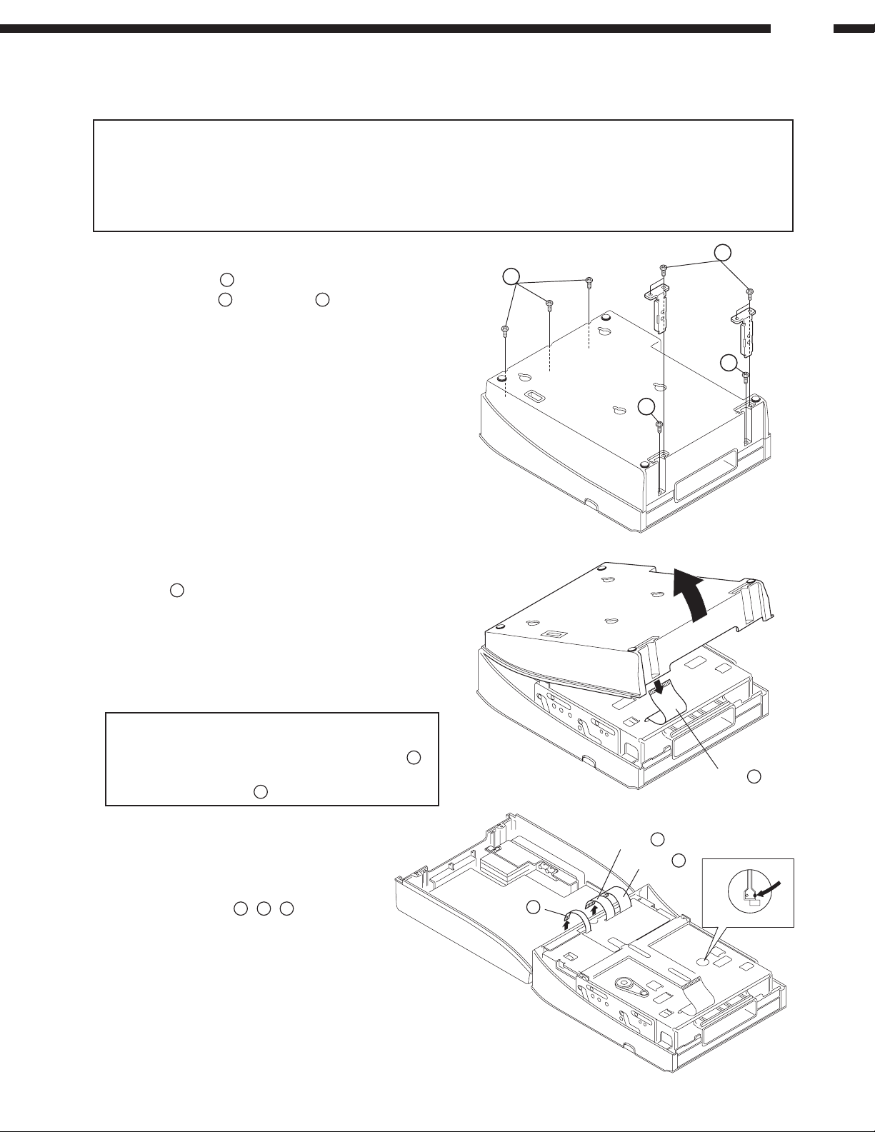
1. Rear Panel
1) Remove 4 screws 1 to detach the Stand Bracket.
2) Remove 3 screws
3) Lift up bottom end of the Rear Panel and disconnect
the cable
A
2
and 2 screws 3 on the Rear Panel.
.
1
2
3
3
4) Open the Rear Panel, and solder the Shorting Land on
the PWB to short-circuit.
Note:The Shorting Land must be short-circuited to
protect laser diode of the optical pick-up. Be sure
to short-circuit before disconnecting the cable
B
Also, remove solder on the Shorting Land after
inserting the cable
5) Disconnect 3 cables
B
.
B, C, D
.
.
A
Cable
B
Cable
C
Cable
D
Cable
3
D-107
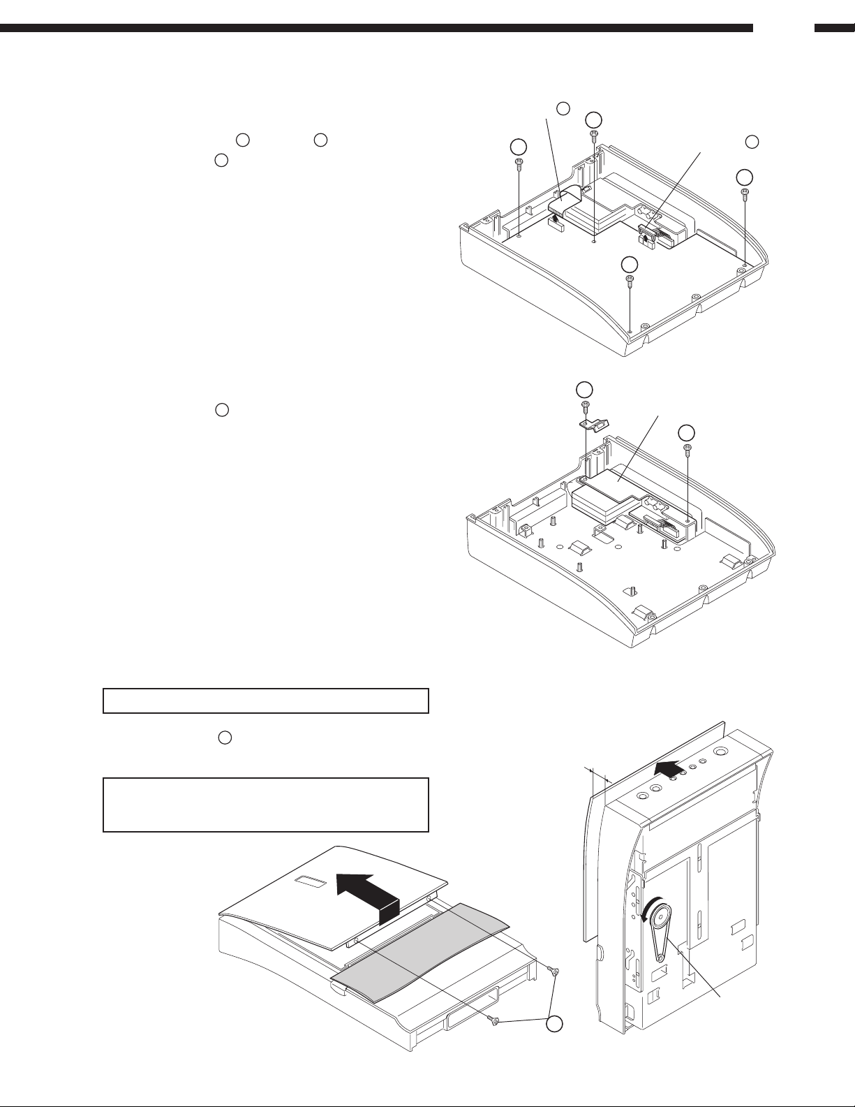
2. Main P.W.B.
1) Disconnect connector A and cable E.
2) Remove 4 screws
4
.
3. I/O P.W.B.
1) Remove 2 screws 5.
Cable
4
E
4
Connector
4
A
4
5
I/O P.W.B.
5
4. Door Panel
1) Turn the pulley counter-clockwise to open the Door
about 10mm horizontally.
Note:Be careful not to disengage or twist the belt.
6
2) Remove 2 screws
direction.
Note:In order not to scratch the silver part of the display
window, cover its surface with a thin sheet
beforehand.
, and detach by lifting in the arrow
10mm
Belt
6
4
D-107
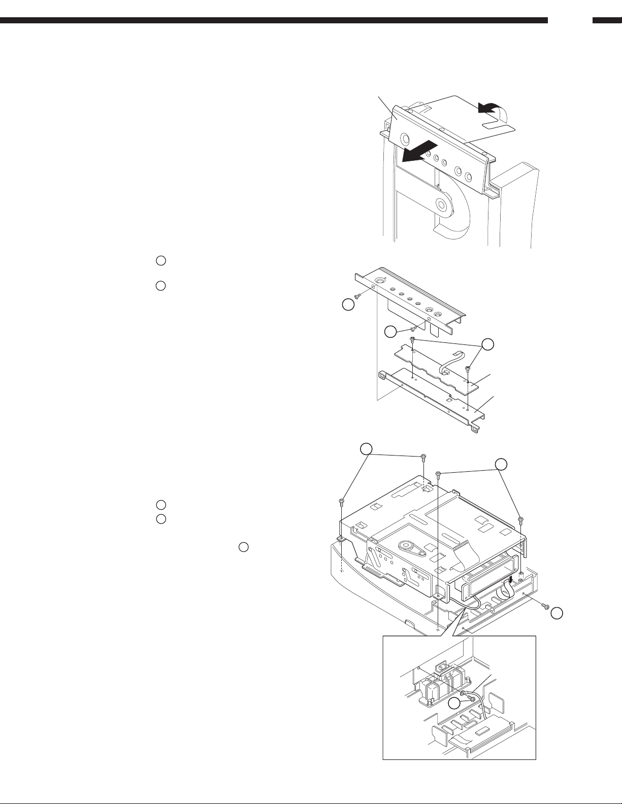
5. Top Panel
1) Open rear of the Top Panel in the arrow direction (A).
2) Pull it out horizontally as shown in the arrow direction (B).
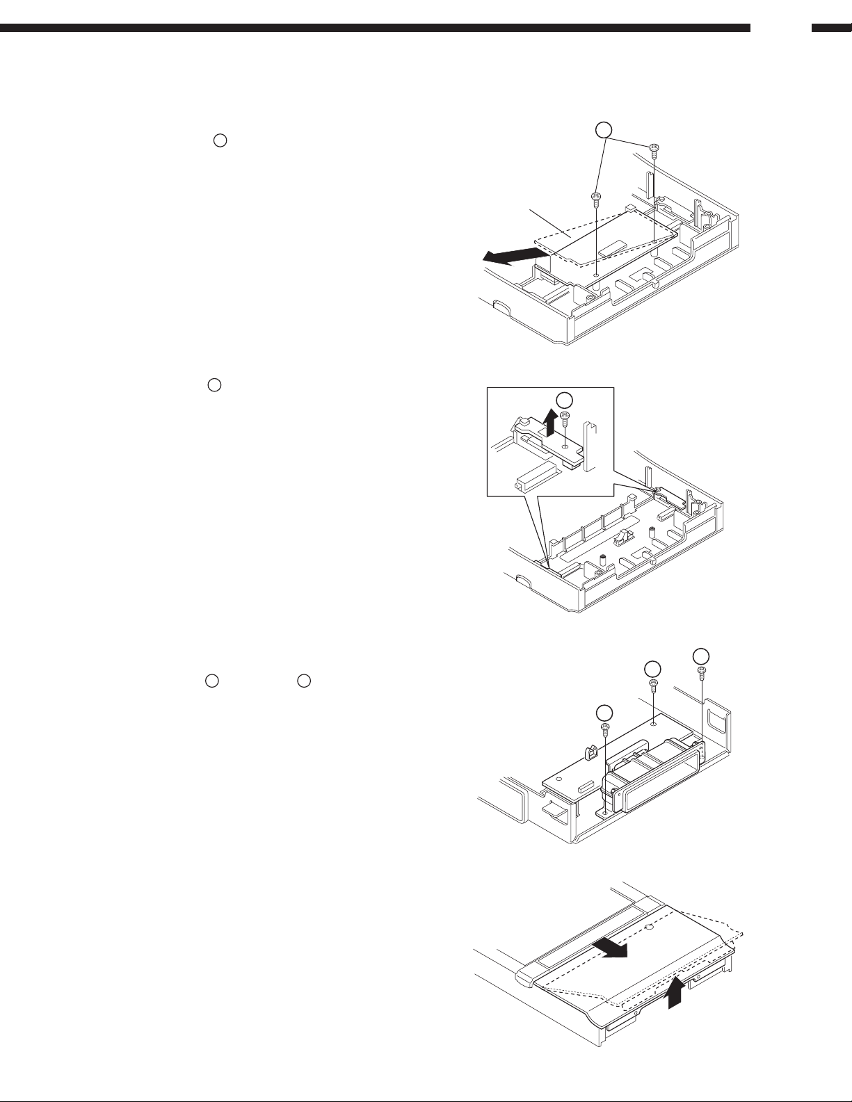
6. Control P.W.B.
1) Remove 2 screws 7 to separate the Top Panel and Tact
Knob Bracket.
2) Remove 2 screws 8.
Top Panel
7
(A)
(B)
7
8
Control P.W.B.
7. Mecha. Unit
1) Remove 4 screws 9.
2) Remove 2 screws
3) Lift up the Mecha. and disconnect the cable.
4) Open the Mecha. and remove 1 screw
.
fixing the wire.
Tact Knob Bracket
9
9
Wire
5
D-107
8. Display P.W.B.
1) Remove 2 screws .
2) Detach the P.W.B. with lifting as shown and sliding in the
arrow direction.
9. OP/CL SW P.W.B., Play P.W.B.
1) Remove 1 screw !.
2) Detach the P.W.B. by moving to the arrow direction.
(The same for the other P.W.B., right and left symmetrical.)
Display P.W.B.
!
10. Interface P.W.B.
1) Remove 1 screw " and 2 screws #, and release the wire
from its clamper.
11. Front Panel
1) Move the Front Panel to the arrow direction (A).
2) Detach the Front Panel with lifting its bottom and sliding in
the arrow direction (B).
"
#
#
(A)
(B)
6
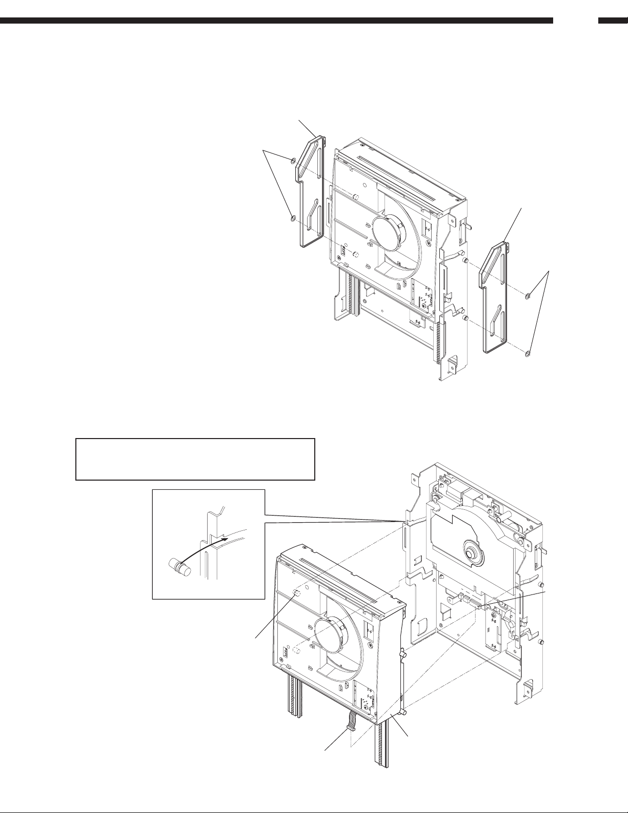
TR MECHA SUB ASS'Y DISASSEMBLY
1. Remove 4 Cut Washers and 2 Slide
Cams on both sides of the Mecha.
Slide Cam
Cut Washer
D-107
Slide Cam
Cut Washer
2. Disconnect 10P ZH-ZH Connector Cord from CX101, then
detach the Door Ass’y.
Note:When re-assembling Door Ass'y, align the groove
on Door Shaft P with the slit of Mecha Chassis
respectively.
Door Shaft P
CX101
10P ZH-ZH Conn. Cord
Door Ass'y
7
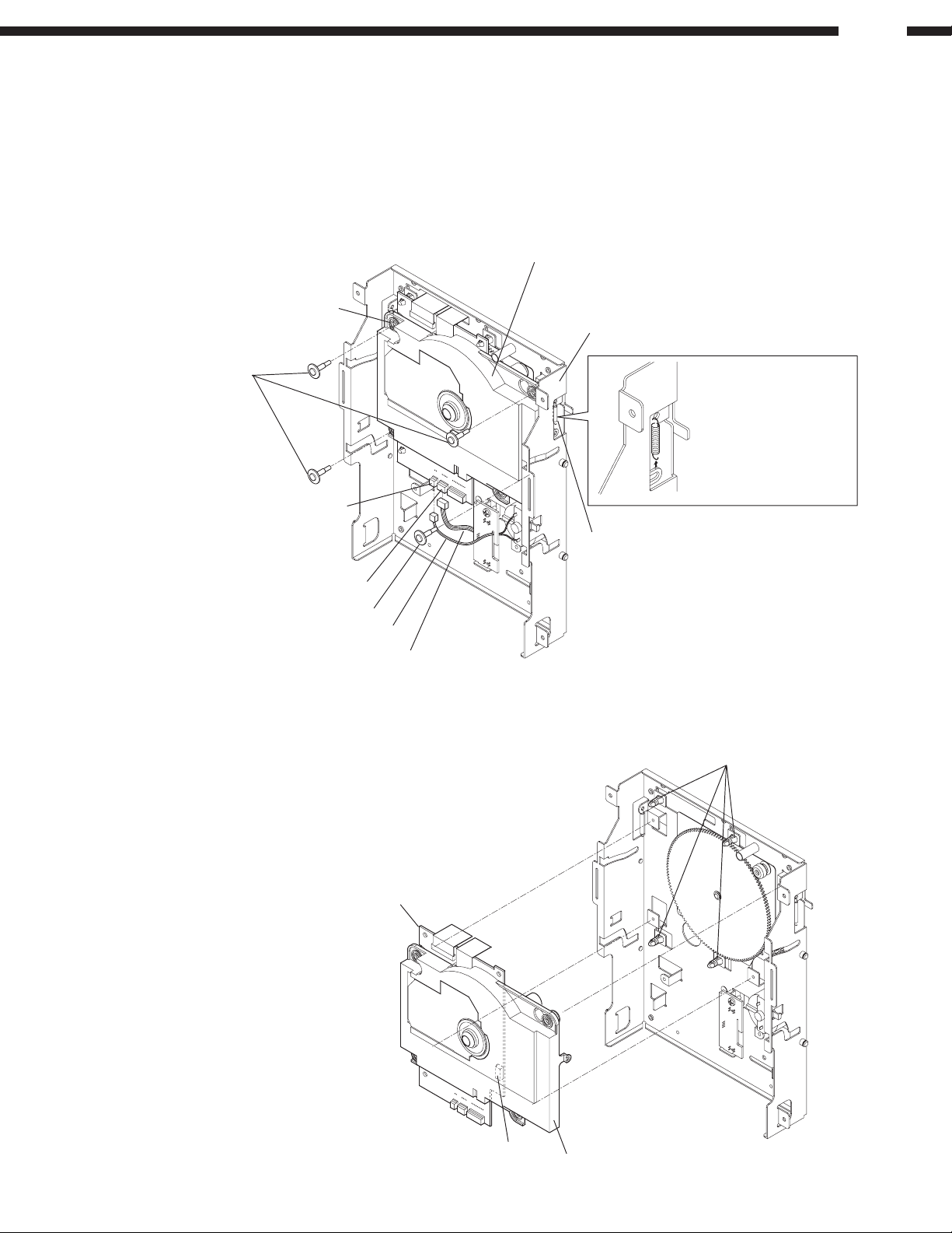
3-1. Disengage one each side of 2 TR Springs. Only TR
Holder side, don’t disengage Mecha Chassis side.
3-2. Disconnect 2P ZR Connector Cord from CX021, and
4P ZH-ZH Connector Cord from CX042.
3-3. Remove 4 pcs of Special Screw fixing the TR Holder.
TR Spring
Special Screw
D-107
TR Holder
Mecha Chassis
Disengage TR Holder
side (lower hook) only
CX021
CX042
Special Screw
2P ZR Conn. Cord
4P ZH-ZH Conn. Cord
4-1. Release 4 PWB Holders for IF Unit.
4-2. Detach IF Unit and TR Holder from the Mecha.
4-3. Disconnect 6P Wire of CD Traverse from CX064.
IF Unit
TR Spring
P.W.B. Holder (H=6.35)
CX064
TR Holder
8
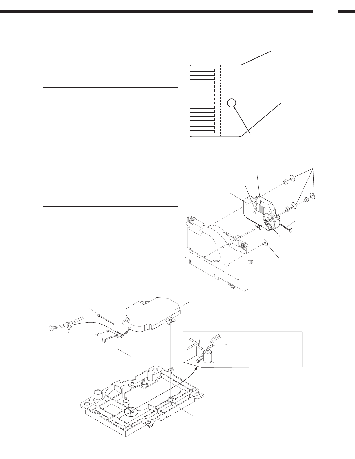
5. Short-circuit the Shorting Land on FPC of TR Mecha Sub
Ass'y by soldering on the pattern.
D-107
Note:Be sure to short-circuit while FPC is still connected
with IF Unit. Also, remove solder on the Shorting
Land after connecting it with IF Unit.
6-1. Detach FPC of TR Mecha Sub Ass'y from IF Unit, then
disconnect it from CX162.
6-2. Remove 4 pcs of 2.6×6 Screw on the back of the TR
Holder, then detach the TR Mecha Sub Ass'y.
Note:When re-assembling the TR Mecha Sub Ass'y, tie
6P wire with a wire clamper and position it between
boss and rib as shown below, then fix with 2.6×6
Screw(p)-Z.
Pick-up
SF-P200R FPC
Seen from the
pattern side
Shorting Land
2.6×6 Screw(P)-Z
FPC
FPC
TR Mecha Sub Ass'y
6P Wire
Short Patter
Wire Clamper
Uncut length: 1~2mm
2.6×6 Screw(P)-Z
TR Mecha Sub Ass’y
38±2
Rib
Arrange the wire so that the
wire clamp comes to the
TR Mecha side.
Boss
TR Holder
9
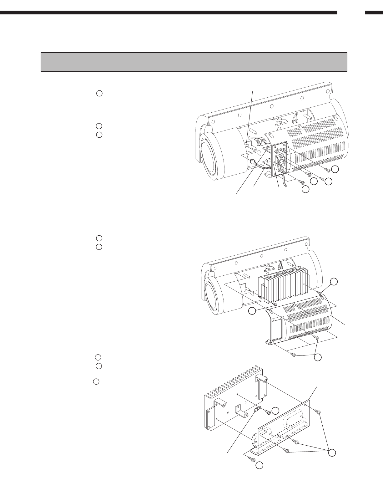
SUB WOOFER DISASSEMBLY
Caution:Be sure to check that there is no jarring sound from sub-woofer or no air-leak through joints of parts after
reassembling by playing CD source (ordinary music source) with volume indication level 30.
D-107
1. SP Terminal Unit, System Conn. Unit
1) Remove 4 screws 1 to detach the Rear Plate.
2) Disconnect 1 cable from the AC Conn. Unit and 3 cables
from the System Conn. Unit.
3) Disengage fasten terminal on SP Terminal right.
4) Remove 2 screws
5) Remove 2 screws
2
to detach the System Conn. Unit.
3
to detach the SP Terminal Unit.
2. Radiator Sub Ass'y
1) Remove 6 screws 4 to detach the Amp Cover.
5
2) Remove 4 screws
3) Lift up the Radiator Sub Ass’y and disconnect 4 cables
from the Power Amp Unit.
fixing the Radiator Sub Ass’y.
AC Conn. Unit
System Conn. Unit
Connect
Rear Plate
1
3
2
1
4) Remove 3 screws
5) Remove 4 screws
Amp Unit.
6) Remove 1 screw
6
and separate the Power Supply Unit.
7
and separate the L/R Amp Unit, SW
8
and separate the PTH Unit.
5
5
Amp Cover
4
Power Supply Unit
8
6
PTH Unit
7
10
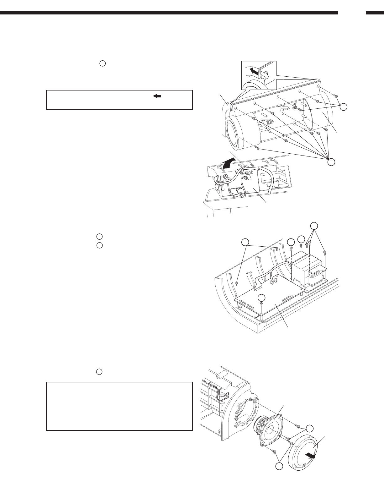
3. Back Cabinet, Front Cabinet
1) Remove 10 screws 9.
2) With holding the Back Cabinet, pull both sides of the Front
Cabinet in the arrow direction.
D-107
Note:Use a rubber hammer etc. to hit the
of the Front Cabinet if it’s hard to remove.
3) Push the Front Cabinet to the arrow direction to make a
gap between the Back Cabinet.
4) Cut the wire clamp band near the Front Cabinet, and
disconnect 4 cables on the Pre Amp Unit.
5) Disconnect 2 cables on the bottom of the Pre Amp Unit,
and separate the Back and Front Cabinet.
arrow part
4. Pre Amp Unit, Transformer
1) Remove 4 screws to detach the Pre Amp Unit.
2) Remove 4 screws
to detach the Transformer.
Front Cabinet
Wire Clamp
Band
Pre Amp Unit
9
Back Cabinet
9
5. Speaker Unit
1) Pull out the Decoration Ring in the arrow direction.
2) Remove 4 screws
Note:When disconnecting the cables from terminals of
the Speaker Unit, make it at the position where the
terminals of the Speaker Unit can be seen from the
Back Cabinet. The clamp part of the internal
speaker cables will be disengaged if separated
farther.
to detach the Speaker Unit.
Speaker Unit
Pre Amp Unit
Decoration Ring
11
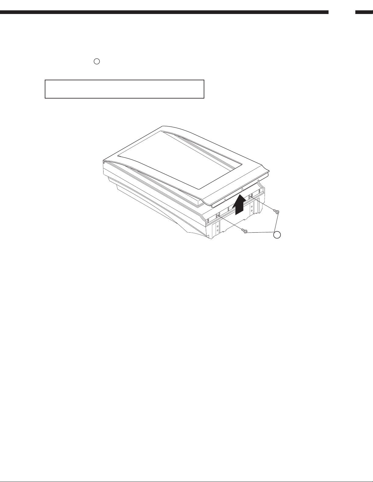
SPEAKER DISASSEMBLY
1. Front Panel
1) Remove 2 screws 1.
2) Lift up bottom end of the Front Panel as shown to release the hook.
Note: Unit change will be necessary if farther disassembling is
needed.
D-107
1
12
D-107
NOTE IN HANDLING FOR LASER PICK-UP
Caution for Handling the Laser Pick-up
The laser pick-up is assembled and precisely adjusted using a sophisticated manufacturing process in our plant. Do not
disassemble or attempt to readjust it. Please observe the following instructions carefully in handling the pick-up.
1. Handle with Care
(1) Storage
Do not store the pick-up in dusty, high-temperatured or high-humidity environments.
(2) Please take care for preventing from shock by falling down or careless handling.
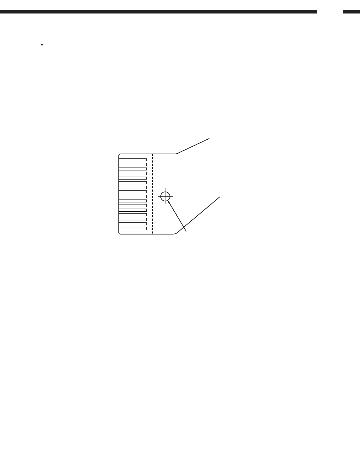
2. Protection of the LD
Short a part of the LD circuit by soldering. After connection to a circuit, remove the short solder.
Pick-up
SF-P200R FPC
Seen from the
pattern side
Shorting Land
3. Precautions when handling the CD mechanism
Handle the laser pick-up so that it is not exposed to dust.
Do not leave the laser pick-up bare. Be sure to cover it.
If dust adheres on lens of the pick-up, blow it off with a blower brush.
Do not shock the laser pick-up.
Do not watch the light of the laser pick-up.
4. Cautions on assembling and adjustment
Be sure that to the bench, jig, head of soldering (with ceramic) iron and measuring instruments are well grounded.
Workers who handle the laser pick-up must be grounded.
The finished mechanism (prior to anchoring in the set) should be protected against static electricity and dust.
The mechanism must be stored so that damaging outside forces are not received.
When carrying the finished mechanism, hold it by the chassis body.
For proper operation, storage and operating environment should not contain corrosive gases. For example H
NO2, CL2 etc. In addition storage environment should not have materials that emit corrosive gases especially from
silicic, cyanic, formailn and phenol group. In the mechanism or the set, existence of corrosive gases may cause no
rotation in motor.
2S, SO2
13
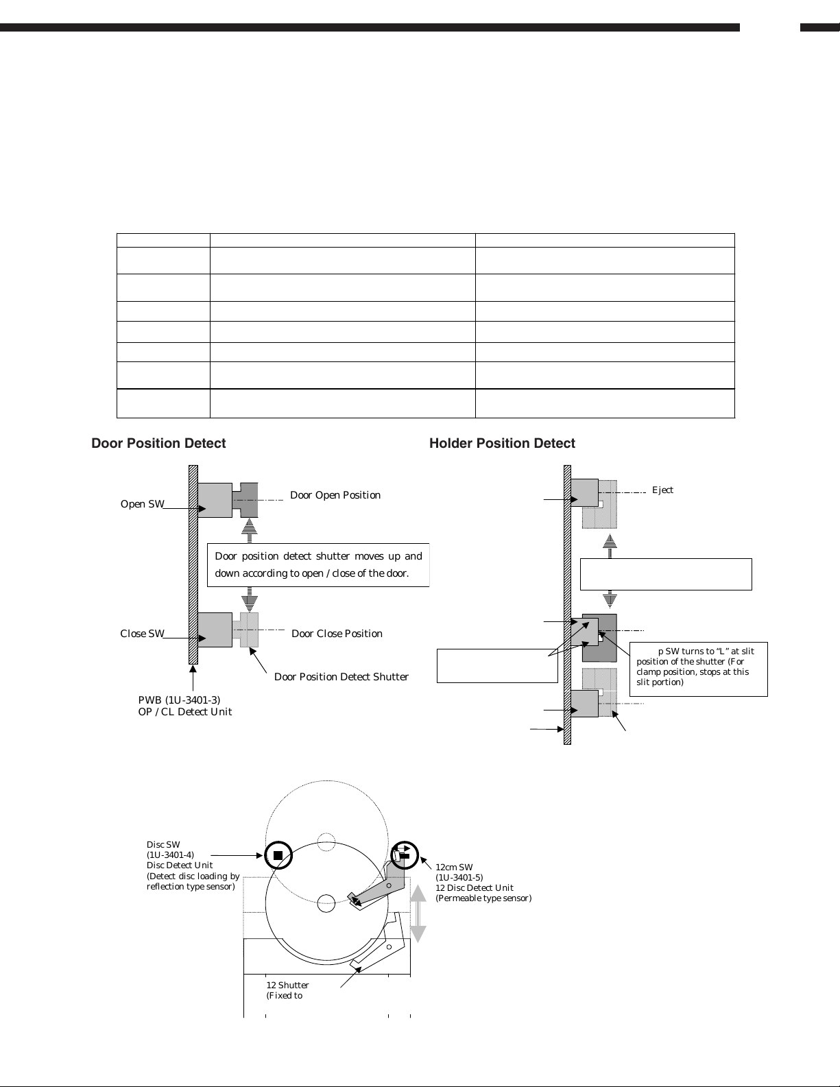
MECHANISM AND FUNCTION OF CD MECHA
Name Function Remarks
Disc SW Disc insertion detect
Monitors at holder (Door Open),
With disc : “L”, without disc : “H”
12cm SW 12cm Disc detect
Monitors at holder eject position,
12cm disc load : “L”, others : “H”
Open SW Door open position detect Door open stop position : “H”, others : “L”
Close SW Door close position detect Door close stop position : “H”, others : “L”
Out SW Holder (disc transfer part) eject position detect Eject position : “H”, others : “L”
Clamp SW Holder (disc transfer part) clamp position detect
Clamp position : “L”, Near Clamp position : “H”
Others : “L”
In SW
(Holder’s disc release position after clamping)
Retract position : “H”, others : “L”
Eject Position
Clamp Position
Out SW
Clamp SW
Holder position detect shutter moves
according to up / down of the holder.
Retract PositionIn SW
Holder Position Detect Shutter
PWB (1U-3401-2)
Disc Up / Down Unit
Near clamp position,
Clamp SW turns to “H”
Clamp SW turns to “L” at slit
position of the shutter (For
clamp position, stops at this
slit portion)
1. Traverse Mecha :
TR Mecha Sub Ass’y (GEN5327)
2. Door Open/Close Mechanism:
Driven by the door open/close motor, Open SW and Close SW are equipped for checking stop position.
3. Disc Transfer Mechanism:
Driven by the holder up-down motor, Out SW, Clamp SW, and In SW are equipped for checking stop position.
Description
Holder (disc transfer part) retract position detect
D-107
Door Position Detect Holder Position Detect
Open SW
Close SW
PWB (1U-3401-3)
OP / CL Detect Unit
Door position detect shutter moves up and
down according to open / close of the door.
Door Open Position
Door Close Position
Door Position Detect Shutter
Disc Detect
Disc SW
(1U-3401-4)
Disc Detect Unit
(Detect disc loading by
reflection type sensor)
12 Shutter
(Fixed to holder, actuates 12cm SW when pushed by 12cm
disc’s edge, immovable with 8cm disc)
12cm SW
(1U-3401-5)
Disc Detect Unit
12
(Permeable type sensor)
14
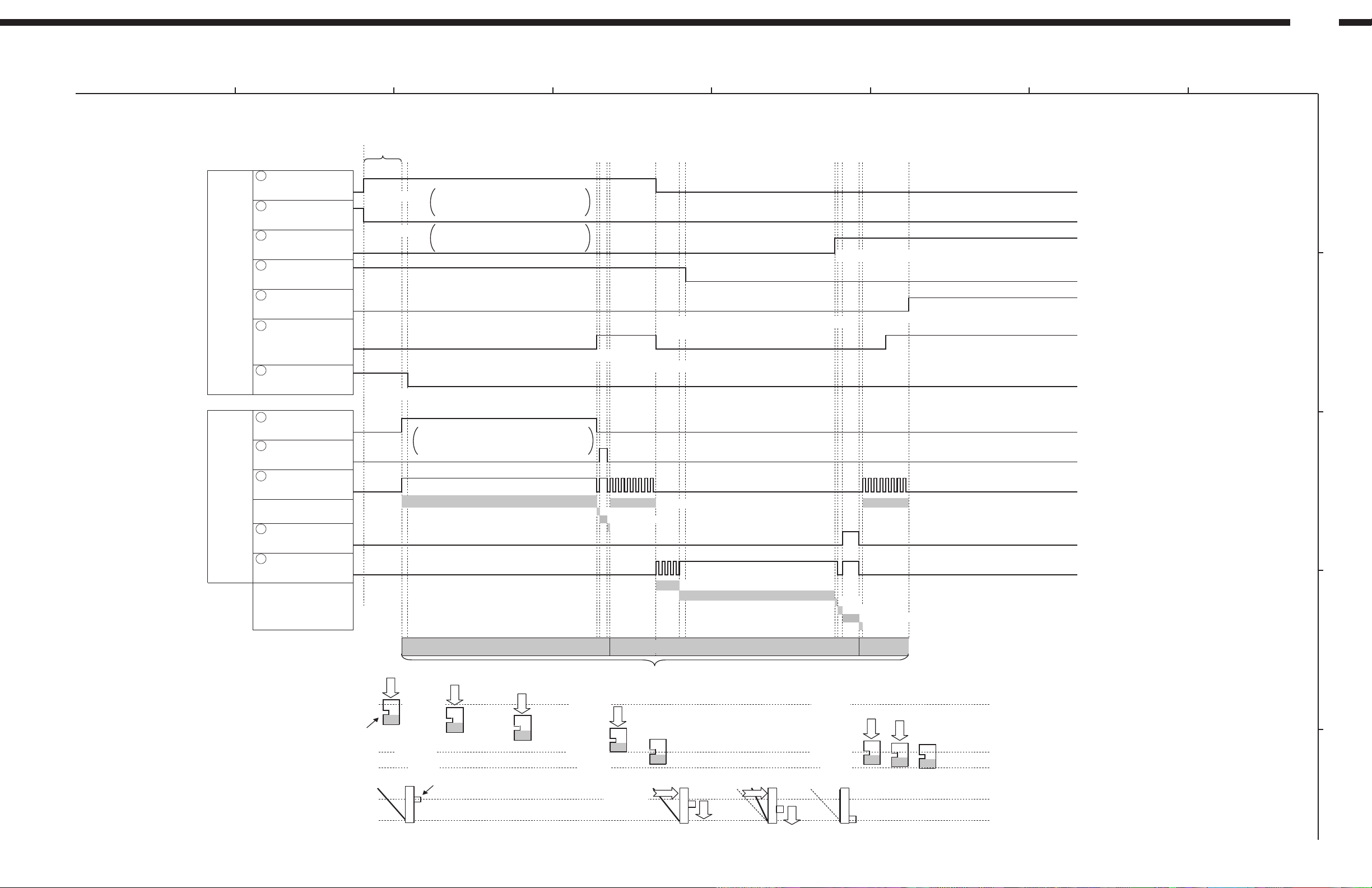
D-107
1 5678
Loader Mecha Timing Chart
Timing Chart when close
49 pin
DISC_SW
50 pin
12cm_SW
46 pin
CLOSE_SW
IC101
µcom
Input
Port
47 pin
OPEN_SW
43 pin
IN_SW
(Retract Position)
44 pin
CLAMP_SW
(Clamp Position)
45 pin
OUT_SW
(Eject Position)
Hi
Lo
Hi
Lo
Hi
Lo
Hi
Lo
Hi
Lo
Hi
Lo
Hi
Lo
1 sec.
↑ 1. Disc Detect
↑ 1. Disc Detect
↑ 2. Holder Down Start
32
Descends holder after 1sec. when
DISC_SW(H) and 12cm_SW (L)
conditions are satisfied.
Defines as 8cm disc insertion in case of
DISC_SW(H) and 12cm_SW (H), and
repeats holder up/down 10 times.
4
↓ 6. Door Close Start (pulse open 4 times + door open)
↓ 5. Holder Slowdown End (pulse decline stop)
↑ 3. Holder Down Stop
↑ 4. Holder Slowdown Start (pulse decline start)
A
↑ 7. Door Close Stop
↓ 9. Holder Retract End (pulse decline stop)
↑ 8. Holder Retract Start (pulse decline start)
B
IC101
µcom
Output
Port
33 pin
DISC_DOWN
54 pin
Holder Motor (up)
(F. IN)
53 pin
Holder Motor (down)
(R. IN)
56 pin
Door Motor (open)
(FWD)
57 pin
Door Motor (close)
(REV)
Holder
Door
Hi
Lo
Hi
Lo
Hi
Lo
Hi
Lo
Hi
Lo
OUT_SW→
Holder Position
Detect Shutter
CLAMP_SW→
IN_SW→
OPEN_SW→
DISC_DOWN signal: Voltage control terminal
of holder motor which becomes "H" when
descending holder (disc) and "L" when others.
↑ Holder Down (While CLAMP_SW: Lo)
1. Disc Down Section (open corrective period)
(Monitor timer: 6sec.)
DOWN
OUT_SW→ OUT_SW→ OUT_SW→
CLAMP_SW→ CLAMP_SW→ CLAMP_SW→
IN_SW→
DOWN
Door Position
Detect Shutter
DOWN
↑ 20msec, 20msec Pulse Decline (while CLAMP_SW: Hi)
↑ STOP
↑ BRAKE (80msec)
↑ STOP
↑ Close with 20msec, 20msec Pulse (4 times)
↑ Door Close (while CLOSE_SW: Lo)
2. Slowdown Period
(Monitor timer: 2sec.)
Close Monitor Timer: 12sec.
* When monitor time-out, it reverts to open motion
DOWN
IN_SW→
OPEN_SW→
CLOSE
3. Door Close
(Monitor timer: 5sec.)
CLOSE
DOWN
↑ STOP
IN_SW→
DOWN
↑ 10msec, 10msec Pulse Decline (while IN_SW: Lo)
↑ 50msec Wait
↑ BRAKE (200msec)
↑ STOP
4. Retract Section
(Monitor timer: 2sec.)
DOWN
DOWN
C
D
E
15
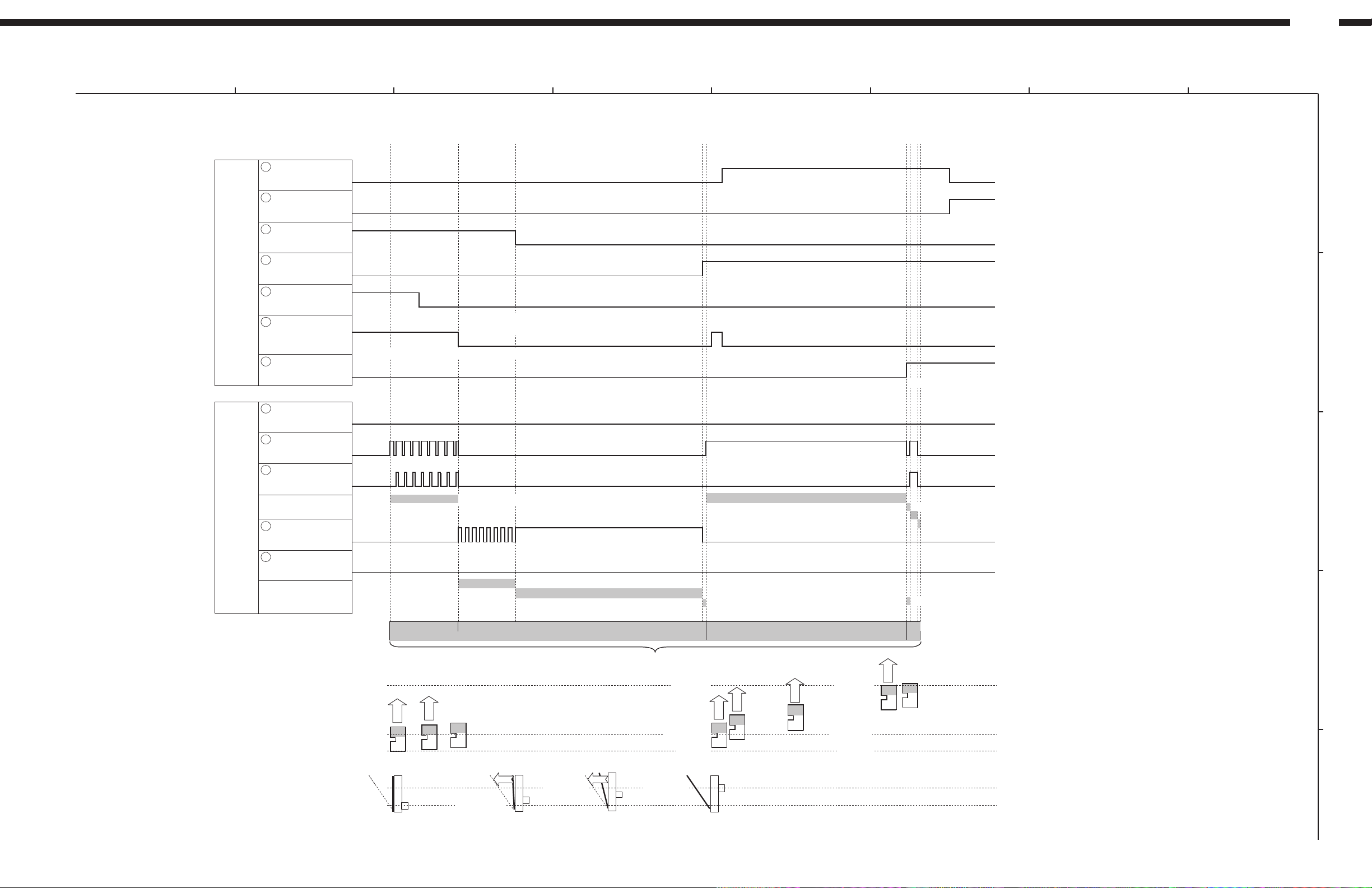
D-107
1 5678
Loader Mecha Timing Chart
Timing Chart when open
IC101
µcom
Input
Port
IC101
µcom
Output
Port
49 pin
DISC_SW
50 pin
8cm_SW
46 pin
CLOSE_SW
47 pin
OPEN_SW
43 pin
IN_SW
(Retract Position)
44 pin
CLAMP_SW
(Clamp Position)
45 pin
OUT_SW
(Eject Position)
33 pin
DISC_DOWN
54 pin
Holder Motor (up)
(F. IN)
53 pin
Holder Motor (down)
(R. IN)
56 pin
Door Motor (open)
(FWD)
57 pin
Door Motor (close)
(REV)
32
Hi
Lo
Hi
Lo
Hi
Lo
Hi
Lo
Hi
Lo
Hi
Lo
Hi
Lo
Hi
Lo
Hi
Lo
Hi
Lo
Hi
Lo
Hi
Lo
↓ Open Key Press
↑ 4. Door Open Start
↓ 3. Door Pulse Open Start (pulse open)
↓ 2. Holder Receiving End (pulse rise stop)
↑ 1. Holder Receiving Start (pulse rise start)
↑ 20msec, 10msec Pulse Rise (while CLAMP_SW: Hi)
(10msec BREAK)
↑ 20msec, 20msec Pulse Open (while CLAMP_SW: Hi, or 15 times)
↑ Door Open (while OPEN_SW: Lo)
4
↓ Unload Disc
A
↑ 5. Door Open Stop
↑ 6. Holder Up Start
B
↑ 7. Holder Up End
↑ Holder Up (while OUT_SW: Lo)
↑ STOP
↑ STOP
↑ BREAK (200ms)
↑ STOP
↑ STOP
C
Holder
Door
OUT_SW→
CLAMP_SW→
IN_SW→
OPEN_SW→
CLOSE_SW→
1.
Receiving Period
(Monitor timer: 2sec.)
UP
UP
CLOSE_SW→
2. Door Open Section
(Monitor timer: 5sec.)
OPEN
OPEN_SW→
Close Monitor Timer: 12sec.
* It stops when monitor time-out
OPEN
OPEN_SW→
OUT_SW→
CLAMP_SW→
IN_SW→
3. Disc Up Section (open corrective period)
(Monitor timer: 6sec.)
UP
UP
UP
OUT_SW→
CLAMP_SW→
IN_SW→
4. Open Finish Section
D
UP
E
16
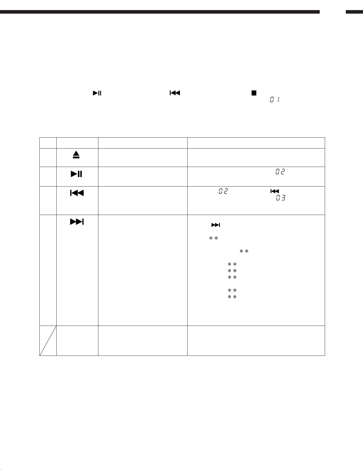
CONFIRMATION METHOD OF ADJUSTMENT
In the µcom of this system, there is a built-in function “adjustment confirmation mode” to
check various servo control easily with CD operation buttons.
Also, focus offset, tracking offset, tracking balance, focus gain, and tracking gain are all
adjusted automatically as the digital servo control is built in the system.
1. Activating Adjustment Confirmation Mode
(1) Load the test disc TCD-784 or Mozart (CO-74176) at the function CD.
(2) After pressing the button (PLAY/PAUSE) and button simultaneously, press button (STOP) within 3 sec.
(The adjustment confirmation mode is activated and the track number of the display turns to
Note: Normal control is disabled with the operation buttons when the adjustment confirmation mode is activated.
To cancel this mode, simply unplug the AC cord.
2. Function of Adjustment Confirmation Mode
.)
D-107
Step
(0)
(OPEN/CLOSE)
(1)
(PLAY/PAUSE)
(2)
(3)
Button Function
Load / unload of disc. Open/close while disc is no rotation.
Activates focus servo, and
starts disc rotation.
Activates all servo, and starts
auto-adjustment.
Displays each
auto-adjustment result.
Description
Press other button after finishing open/close mode.
Track number display turns to .
When displayed, press after 3 sec.
Track number display turns to .
After auto-adjustment, it stops.
After finishing auto-adjustment, every pressing of
the button displays each adjusted value of
auto-adjustment as follows. Check that the value
of portion falls within the range shown Table 1
on page18.
(The value of
Fdoffset h (Focus offset adjusted value)
Tdoffset
Tbal h
Fbal 0 0 h (Focus balance adjusted value)
Fogain
Trgain h (Tracking gain adjusted value)
Focus balance adjusted value is always fixed to 00h.
portion is hexadecimal)
h (Tracking offset adjusted value)
(Tracking balance adjusted value)
h (Focus gain adjusted value)
Other Button
May not operate normally.
Do not operate with other buttons other than
described above during this mode.
17
D-107
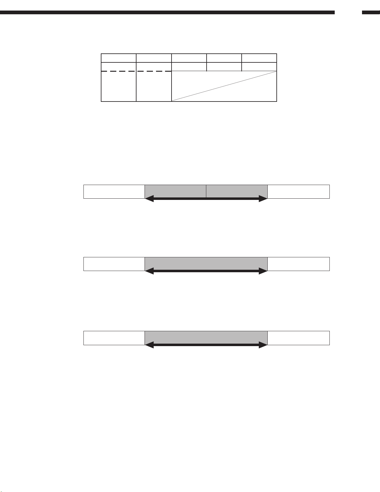
Table1 Servo Adjust Value Confirmation List
Fdoffset Tdoffset Tbal Fogain Trgain
EAh~0Eh EAh~0Eh 6Bh~9Ah 28h~56h 28h~56h
EAh~FFh EAh~FFh
or or
00h~0Eh 00h~0Eh
Fbal value indicated fourth in the item of adjusted value check will be displayed always as 00h because no adjustment is made.
When out of the range value appears, open and close the door once, then check the value again.
Value indicated are hexadecimal
(HEX)
Summary of Adjustment Range
Adjustment and confirmation range of Fdoffset, Tdoffset
Adjustment range: 9Ah ~ 66h
Confirmation range: EAh ~ 0Eh
9Ah EAh FFh
Adjustment and confirmation range of Tbal
Adjustment range: 00h ~ FFh
Confirmation range: 6Bh ~ 9Ah
00h 6Bh
Adjustment and confirmation range of Fogain, Trgain
Adjustment range: 14h ~ 7Fh
Confirmation range: 28h ~ 56h
14h 28h
00h 0Eh
9Ah
56h
66h
FFh
7Fh
18
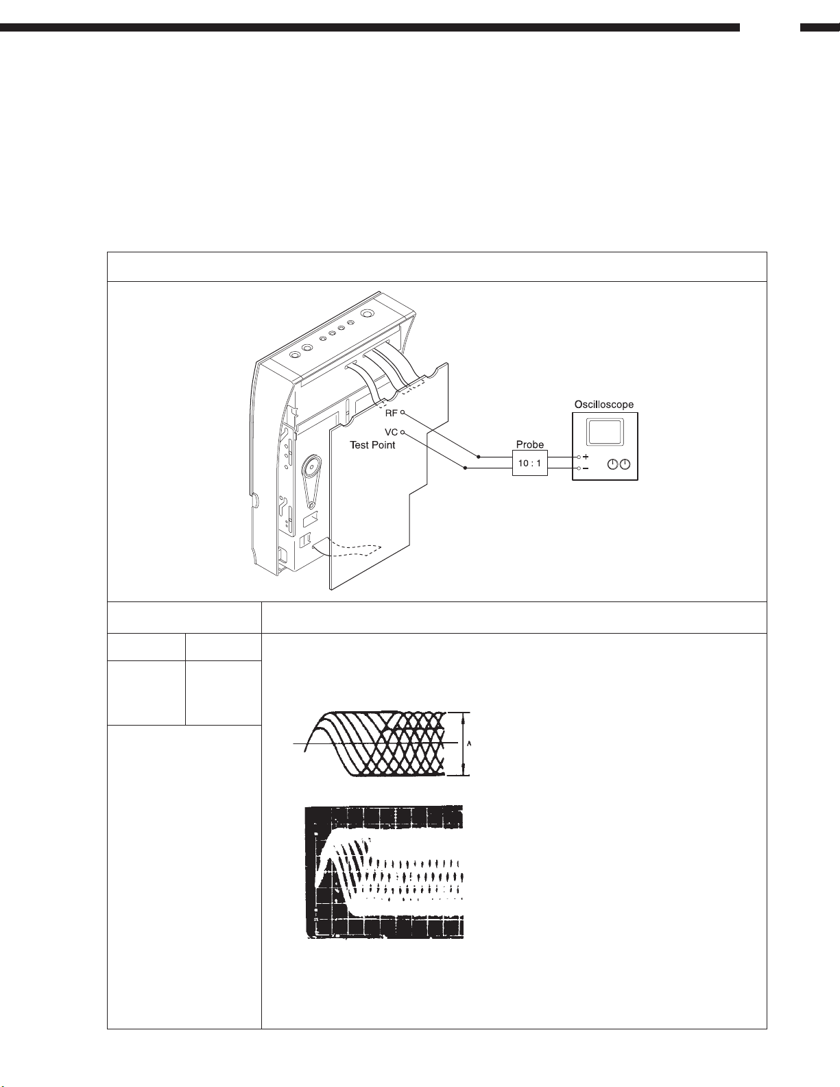
3. How to Check HF Level
(1) Measuring instruments required
a) Oscilloscope
b) Test disc: TCD-784 (A-BEX) or Mozart (CO-74176)
(2) Attaching connection wire for checking HF level
a) Disassemble 1U-3398-1 (Main PWB) → Refer to “DISASSEMBLY” on page 3, 4.
b) Solder wires to RF and VC test points for connecting the probe of oscilloscope.
(Length of the wires should be less than 20 cm) → Refer to 1U-3398-1 drawing on page 32.
c) Assemble 1U-3398-1, see the diagram below.
Wiring Diagram
D-107
Oscilloscope
VH
50mV/div
or
20mV/div
0.2µs/div
or
0.5µs/div
Check Item
1. Playback the test disc.
2. Check HF level on the oscilloscope.
A=0.7V~1.3V
Eye-pattern
3. Check that the wave-form is not deformed
(The center 2 shapes must be discernible.)
19
)
BLOCK DIAGRAMS
D-107
1
32
4
5678
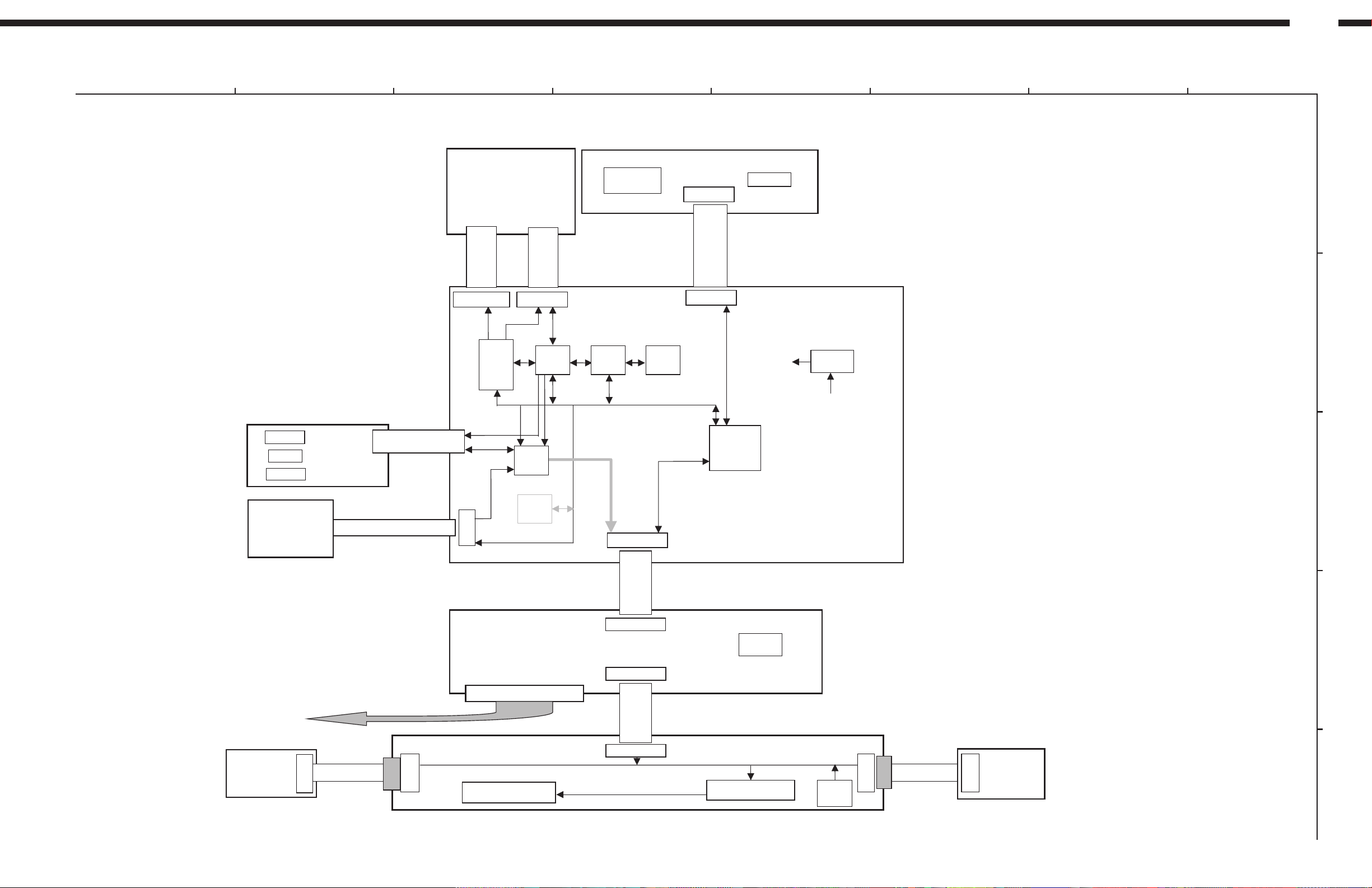
UD-107 BLOCK & WIRING DIAGRAM
FG350
(Mecha side inserted)
21P FFC (P=1)
CX161 CX211
IC201
IC202
MOTOR
DRIVER
(Mecha side inserted)
16P FFC (P=1)
IC204
DSP
POWER ON/
STANDBY LED
MAIN UNIT
IC203
MP3
1U-3398-7
CONTROL UNIT
1U-3398-8
IC208
DRAM
CY051
5P FFC (P=1)
CX051
TACT SW
IC204
IC203
IC208
IC207
Reg. +3.3V
VVV
+5V-D1
A
B
OPT.OUT
AUX IN
AUX OUT
TUNER PACK
USW-107
1U-3398-5
OP/CL SW UNIT
1U-3398-4
AUDIO I/O UNIT
CW031
3P KR-DS(WHT)
11P TWGP
15P FFC (P=1.25)
CX031
CX151
IC305
EQ&VR
IC302
RDS
20P DISM
FL701 (VFD)
CX291
CY291
1U-3398-3
INTERFACE UNIT
CY131
13P FFC (P=1)29P FFC (P=1)
CX131
1U-3398-2
DISPLAY UNIT
IC101
µ
COM
IC501
Reg. +6V
IC701 VFD DRIVER
IC703
REMOCON
SENSOR
CX032
3P KR-DS (RED)
CW032
1U-3398-6
PLAY SW UNIT
C
D
E
20
D-107
1 5678
32
4
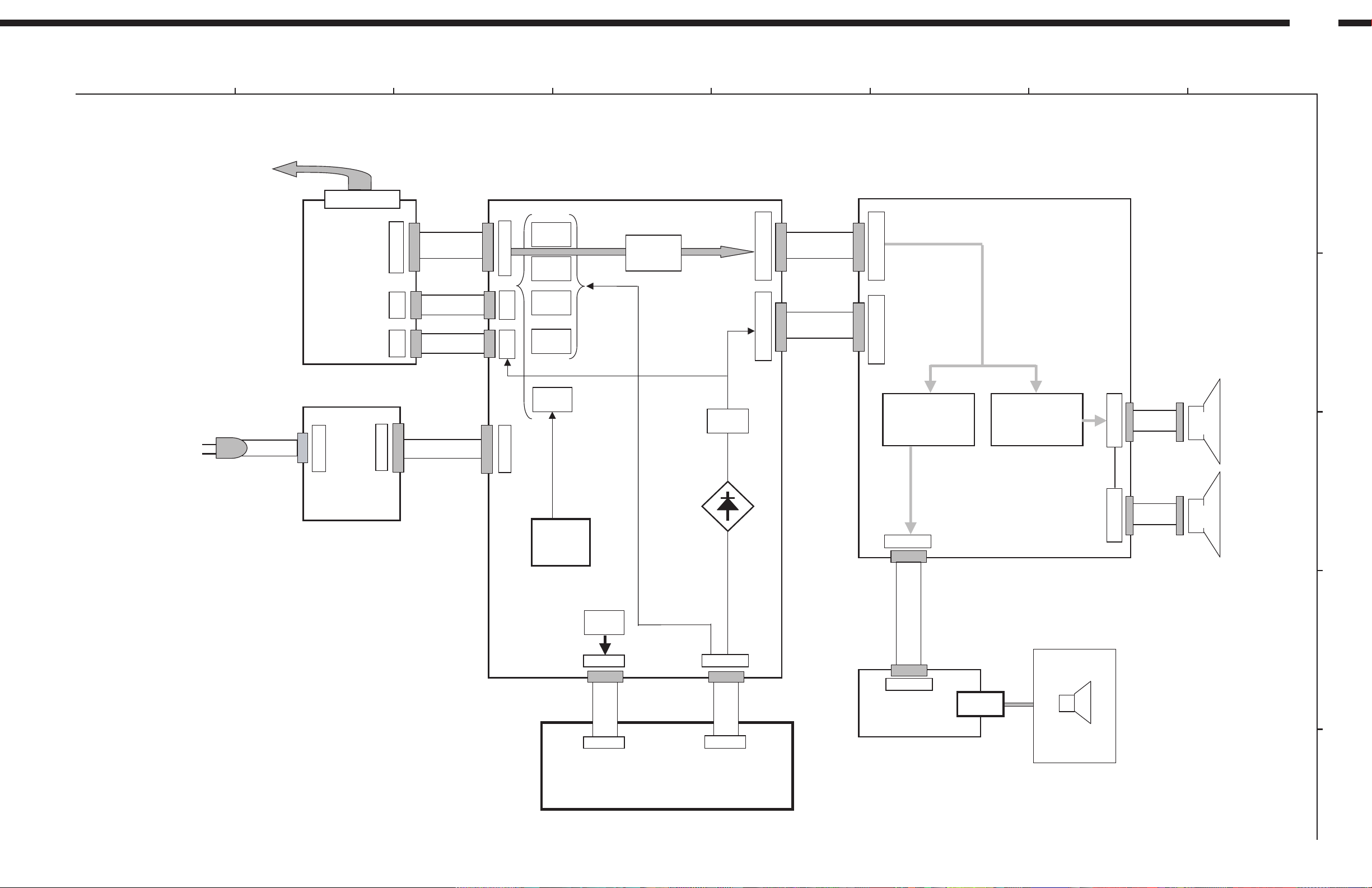
USW-107 BLOCK & WIRING DIAGRAM
UD-107
A
AC CORD
20P DISM
1U-3445-1
SYSTEM CONN
UNIT
1U-3417-6
AC CONN
CX025
UNIT
CY121 CY061 CX031
CY022
12P PH-PH
6P PH-PH
6P PH-PH
2P VH-VH (BLU)
CX121
CX061
CY031
CX022
IC201
Reg. +12V
IC202
Reg. +6V
TR201
Reg. -30V
DC
+/-F
IC203
Reg. +6V
1U-3400-1
POWER SUPPLY UNIT
AUDIO SIG.
HPF/LPF
ALC
MAIN AMP
±
V
CX111 CX101
11P PH-PH
10P EH-EH
CY111 CY101
1U-3417-2
L/R AMP UNIT
IC500
STK402-050
1U-3417-1
POWER AMP UNIT
1U-3417-3
SW AMP UNIT
IC700
STK402-050
CX023 CX024
2P EH
B
SW
T202
MINI
TRANS
PRIMARY
RELAY
CX021
2P VH-VH
CW021
1U-3400-2
PRIMARY UNIT
MAIN POWER TRANS
T201
CX131
13P SCN-EH
CW131
1U-3400-3
SECONDARY UNIT
CX041
4P EH-EH
CY041
1U-3417-4
SP TERMINAL
UNIT
JK500
USC107 L/R
2P EH
SW
C
D
E
21
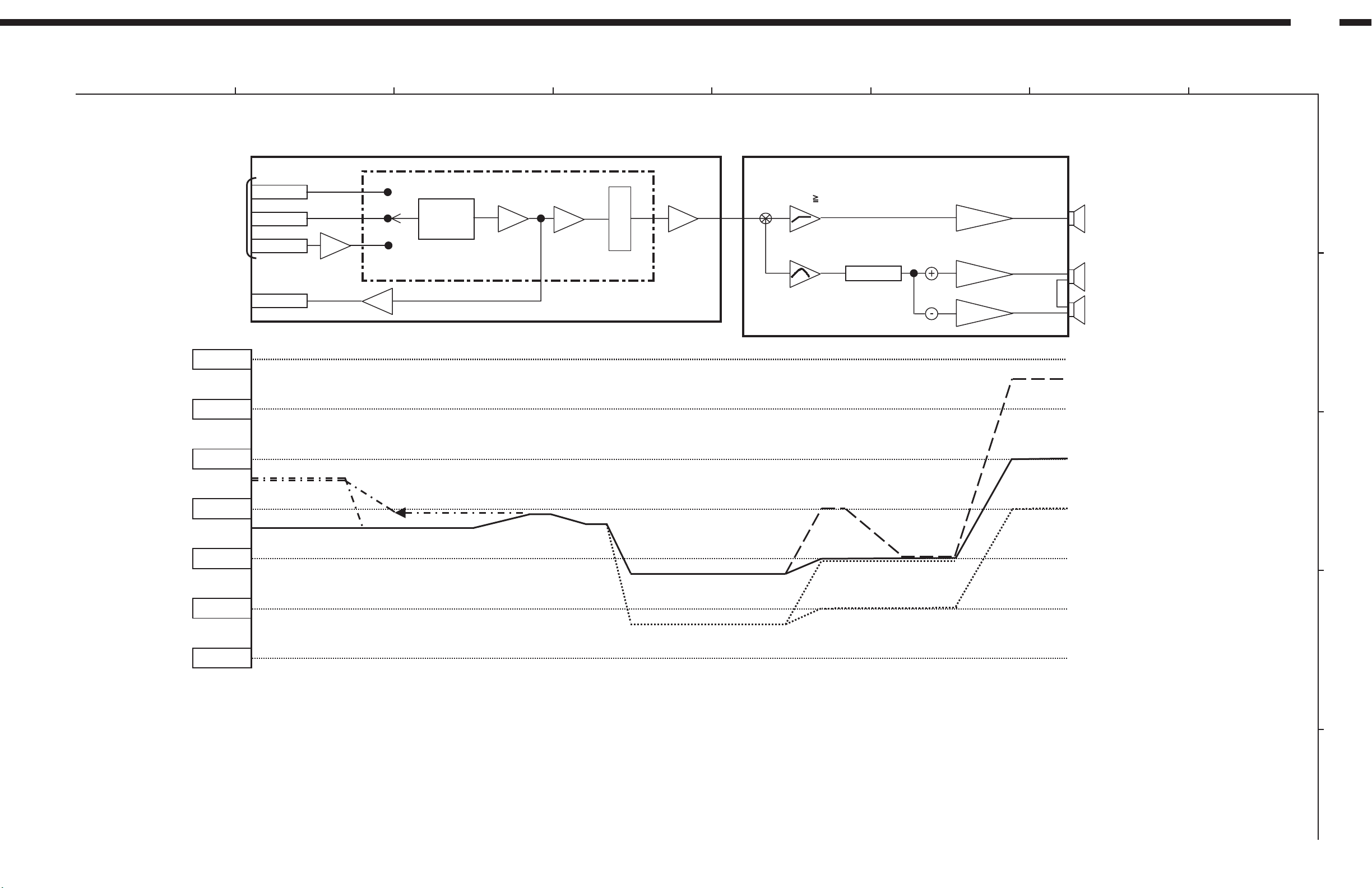
LEVEL DIAGRAM
D-107
1
32
4
5678
D-107 LEVEL DIAGRAM
SOURCE
UD107
TUNER
CD
AUX IN
AUX OUT
LC75396NE
FUNCTION
SWITCH
INPUT
EQ
V
O
L
U
M
E
USW107
HPF 200Hz
BPF PEAK 70Hz
ALC
L/R
POWER AMP
SUB
WOOFER
A
L/R SPEAKER
SUB
WOOFER
B
+30dBV
SUB WOOFER
+20dBV
+10dBV
0dBV
-10dBV
-20dBV
-30dBV
AUX INPUT 2V
CD 0dB
AUX
VOLUME -10dB
STEP54
VOLUME -20dB
STEP44
ALC ON
ALC OFF
L/R
L/R
C
D
E
22
D-107
SEMICONDUCTORS
IC’s
Note: Indication before IC No. (SW) denotes “USW-107”.
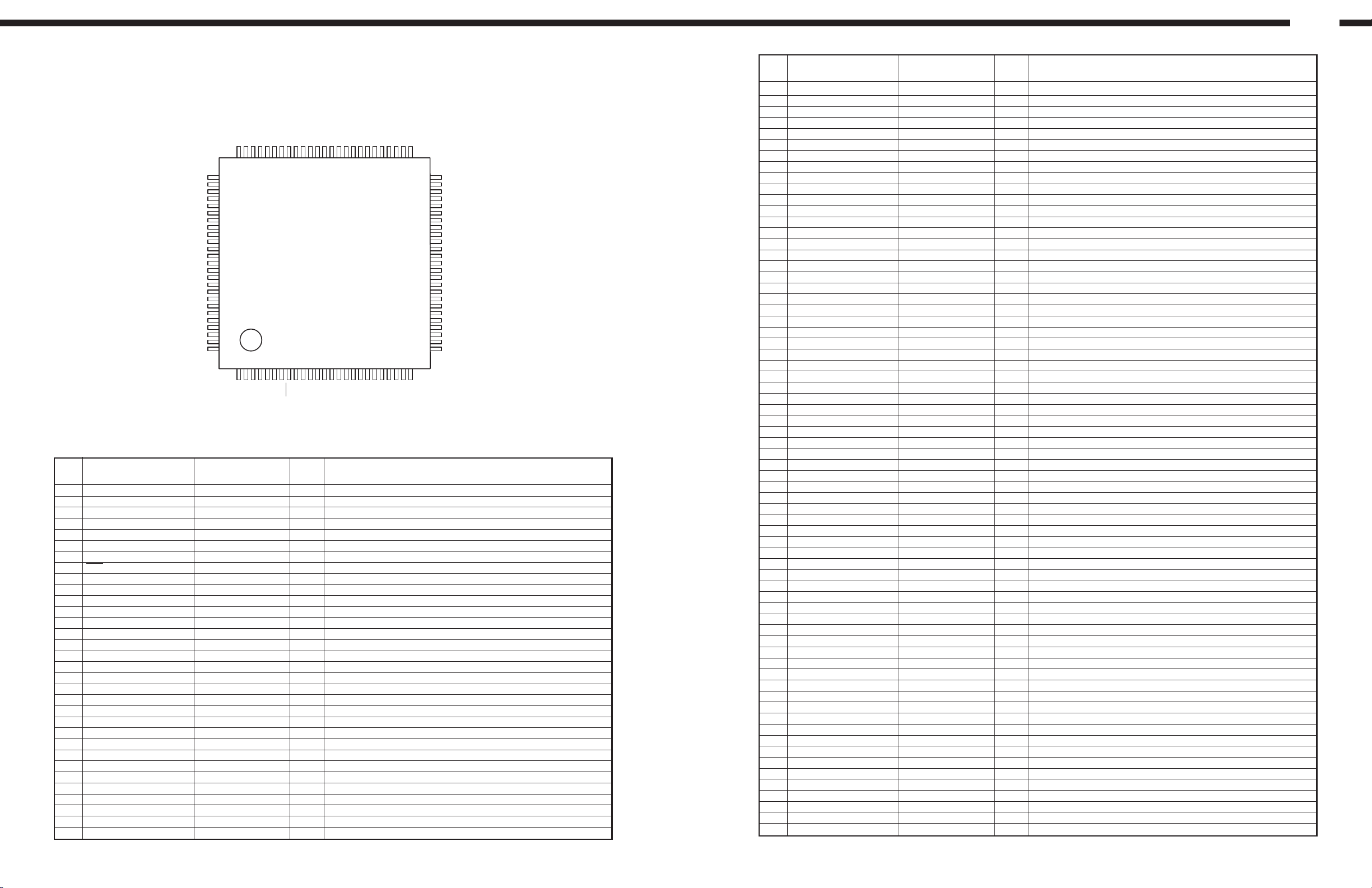
LC877296B
(IC101)
S47/PF7
V3/PL6
V2/PL5
V1/PL4
COM0/PL0
COM1/PL1
COM2/PL2
COM3/PL3
P30
P31
VSS3
VDD3
P32
P33
P34
P35
P00
P01
P02
P03
P04
P05
P06
P07
P10/SO0
M877296B Terminal Function
Pin
No.
1 P11/SI0/SB0 645DO I LC78645, LC78683 serial
2 P12/SCK0 645CK O LC78645, LC78683 serial
3 P13/SO1 SDI O Other PLL, RDS, VR, DISP serial, LC2720, LC72131
4 P14/SI1/SB1 SDO I Other PLL, RDS, VR, DISP serial, LC2720, LC72131
5 P15/SCK1 SCK O Other PLL, RDS, VR, DISP serial, LC2720, LC72131
6 P16/T1PWML 645CE O LC78645CE
7 P17/T1PWMH/BUZ 683CE O LC78683CE
8 RES
9 XT1/AN10 Clock 32.768kHz
10 XT2/AN11
11 VSS1
12 CF1 Main Clock 10MHz
13 CF2
14 VDD1 Back up HOLD mode use
15 P80/AN0 AD0 Operation button input
16 P81/AN1 AD1 Operation button input
17 P82/AN2 AD2 PWB check mode control
18 P83/AN3 AD3 PWB check mode control
19 P84/AN4 ROM CLK I FLASH Write
20 P85/AN5 TUNER1 I Tuner type E20, E31, J1, E10
21 P86/AN6 TUNER2 I Tuner type E20, E31, J0, E11
22 P87/AN7/MICIN OP/CL I Sensor OP/CL input (A/D input)
23 P70/INT0/T0LCP/AN8 FSYNC I LC78683
24 P71/INT1/T0HCP/AN9 INTB I LC78683
25 P72/INT2/T0IN P.DOWN I Power-down detect→HOLD mode
26 P73/INT3/T0IN REMOCON I Remote control input
27 S0/PA0
28 S1/PA1
29 S2/PA2
30 S3/PA3
31 S4/PA4
32 S5/PA5 DISC LED O DISC LED ON output, Hi: ON
Pin Name
S46/PF6
S45/PF5
S44/PF4
S43/PF3
S42/PF2
S41/PF1
S40/PF0
S39/PE7
S38/PE6
S37/PE5
S36/PE4
S35/PE3
S34/PE2
S33/PE1
S32/PE0
S31/PD7
S30/PD6
S29/PD5
S28/PD4
S27/PD3
S26/PD2
S25/PD1
S24/PD0
VSS2
75747372717069686766656463626160595867565554535251P72/INT2/T0IN
76
77
78
79
80
81
82
83
84
85
86
87
88
89
90
91
92
93
94
95
96
97
98
99
100
1P11/SI0/SB0
Symbol
2P12/SCK0
3P13/SO1
4P14/SI1SB1
TOP VIEW
5P15/SCK1
6P16/T1PWML
7P17/T1PWMH/BUZ
8RES
9XT1/AN10
10XT2/AN11
11VSS1
I/O
12CF1
13CF2
14VDD1
15P80/AN0
16P81/AN1
17P82/AN2
18P83/AN3
19P84/AN4
20P85/AN5
21P86/AN6
22P87/AN7/MICIN
23P70/INT0/T0LCP/AN8
24P71/INT1/T0HCP/AN9
VDD2
S23/PC750
49 S22/PC6
48 S21/PC5
47 S20/PC4
46 S19/PC3
45 S18/PC2
44 S17/PC1
43 S16/PC0
42 S15/PB7
41 S14/PB6
40 S13/PB5
39 S12/PB4
38 S11/PB3
37 S10/PB2
36 S9/PB1
35 S8/PB0
34 S7/PA7
33 S6/PA6
32 S5/PA5
31 S4/PA4
30 S3/PA3
29 S2/PA2
28 S1/PA1
27 S0/PA0
26 P73/INT3/T0IN
25
Function
Pin
No.
Pin Name
Symbol
I/O
Function
33 S6/PA6 DISC DOWN O Drive V switching at DISC DOWN, Hi: ON
34 S7/PA7 DSP OSC OFF O XTI OFF other than CD FUNCTION
35 S8/PB0 DRF I LC78645
36 S9/PB1 WRQ I LC78645
37 S10/PB2 EMPH O LC78645
38 S11/PB3 645RST O LC78645
39 S12/PB4 OVF I LC7868
40 S13/PB5 CNTOK I LC7868
41 S14/PB6 WOK O LC7868
42 S15/PB7 683RST O LC7868
43 S16/PC0 IN SW I HOLDER part SW input
44 S17/PC1 CLMP SW I HOLDER part SW input
45 S18/PC2 OUT SW I HOLDER part SW input
46 S19/PC3 DOOR CL SW I DOOR part SW input
47 S20/PC4 DOOR OP SW I DOOR part SW input
48 S21/PC5 LIMIT SW I PU in-circle SW
49 S22/PC6 DISC I DISC insert detect input, L: Detect
50 S23/PC7 12cm I 12cm DISC detect input, H: Detect
51 VDD2
52 VSS2
53 S24/PD0 R.IN O LIFT Motor drive
54 S25/PD1 F.IN O LIFT Motor drive
55 S26/PD2 M.MUTE O LA6559 MUTE
56 S27/PD3 FWD O LA6559 FWD (DOOR Motor)
57 S28/PD4 REV O LA6559 REV (DOOR Motor)
58 S29/PD5 LED RED O Power LED RED
59 S30/PD6 LED GRN O Power LED GRN
60 S31/PD7
61 S32/PE0
62 S33/PE1
63 S34/PE2
64 S35/PE3
65 S36/PE4
66 S37/PE5
67 S38/PE6
68 S39/PE7
69 S40/PF0
70 S41/PF1
71 S42/PF2
72 S43/PF3
73 S44/PF4
74 S45/PF5 396CE O LC75396NE CE
75 S46/PF6 396DI O LC75396NE DI
76 S47/PF7 396CL O LC75396NE CL
77 V3/PL6
78 V2/PL5
79 V1/PL4
80 COM0/PL0
81 COM1/PL1
82 COM2/PL2
83 COM3/PL3
84 P30 ROM DATA0 I/O FLASH Write
85 P31 ROM DATA1 I/O FLASH Write
86 VSS3
87 VDD3
88 P32 DISP RESET Display Driver reset
89 P33 PROTECTION I Power Amp Protection act., L: Detect
90 P34 TUNED I LA1837 Tuned
91 P35 STEREO I LA1837 Stereo
92 P00 SP.RELAY O Speaker Relay, Lo: Mute
93 P01 PRE.MUTE O PRE AMP Mute
94 P02 TU.MUTE O LA1837 Mute
95 P03 DISP.CS O DISPLAY Driver CS
96 P04 AUX MUTE O Mute at AUX Function, Hi: Mute
97 P05
98 P06
99 P07 720CE O LC72720, LC72131 CE
100 S10/SO0 645DI O LC78645, LC78683 serial
39
23
D-107
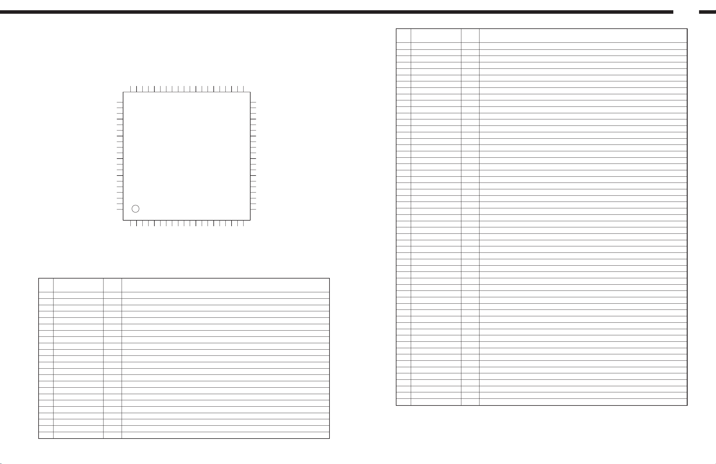
LC78683E (IC203)
MADRS0
MADRS1
MADRS2
MADRS3
MADRS4
MADRS5
MADRS6
MADRS7
60595857565554535251504948
CL
CE
61
62
63
64
65
66
67
68
69
70
71
72
73
74
75
76
77
78
79
80
12345678910111213141516171819
LRSY
ADBCK
ADDATA
ADLRCK
TOP VIEW
VSS
CKIN
C2FIN
VSS
DVDD5
VSS
STREQ
STCK
STDAT
FSYNC
CRCF
DVDD6
VSS
WOK
CNTOK
OVF
CMDOUT
CMDIN
INTB
RESB
DATAIN
DATACK
LC78683E Terminal Function
Pin
No.
Symbol
1 LRSY I CD L/R clock input
2 ADDATA O Audio data output
3 ADBCK O Audio bit clock output
4 ADLRCK O Audio L/R clock output
5 C2FIN I CD C2 flag input
6 VSS GND
7 CKIN I System clock (16.9344MHz) input
8 VSS GND
9 CKOUT O Clock (384Fs) output
10 VSS GND
11 DVDD1 I/O power (3.3V)
12 PW I Sub-code data serial input
13 SBSY I Sub-code block sync sig. input
14 SFSY I Sub-code frame sync sig. input
15 SBCK O Sub-code serial clock output
16 AVDD Analog (PLL) power (3.3V)
17 VPRFR VCO osc. range setting pin
18 VCOC VCO control V input
19 VPDO VCO charge pump output
20 AVSS Analog (GND)
21 DVDD2 Internal power (1.7V)
22 VSS GND
23 MDATA0 I/O DRAM data bus
I/O
VSS
CKOUT
DVDD4
MADRS8
VSS
DVDD1
MADRS9
MADRS10
MADRS11
474546
PW
SFSY
SBSY
OEB
MADRS12
CASUB
444342
SBCK
AVDD
VPRFR
Function
CASLB
WEB
VPDO
VCOC
RASB
41
40
39
38
37
36
35
34
33
32
31
30
29
28
27
26
25
24
23
22
21
20
AVSS
MDATA15
MDATA14
MDATA13
MDATA12
MDATA11
MDATA10
MD ATA9
MD ATA8
VSS
DVDD3
MD ATA7
MD ATA6
MD ATA5
MD ATA4
MD ATA3
MD ATA2
MD ATA1
MD ATA0
VSS
DVDD2
Pin
No.
Symbol
I/O
Function
24 MDATA1 I/O DRAM data bus
25 MDATA2 I/O DRAM data bus
26 MDATA3 I/O DRAM data bus
27 MDATA4 I/O DRAM data bus
28 MDATA5 I/O DRAM data bus
29 MDATA6 I/O DRAM data bus
30 MDATA7 I/O DRAM data bus
31 DVDD3 DRAM I/F power (3.3V)
32 VSS GND
33 MDATA8 I/O DRAM data bus
34 MDATA9 I/O DRAM data bus
35 MDATA10 I/O DRAM data bus
36 MDATA11 I/O DRAM data bus
37 MDATA12 I/O DRAM data bus
38 MDATA13 I/O DRAM data bus
39 MDATA14 I/O DRAM data bus
40 MDATA15 I/O DRAM data bus
41 RASB O DRAM RAS output
42 WEB O DRAM WE output
43 CASLB O DRAM CAS output (Lower Byte)
44 CASUB O DRAM CAS output (Upper Byte)
45 OEB O DRAM OE output
46 MADRS12 O DRAM Address output
47 MADRS11 O DRAM Address output
48 MADRS10 O DRAM Address output
49 MADRS9 O DRAM Address output
50 MADRS8 O DRAM Address output
51 DVDD4 DRAM I/F power (3.3V)
52 VSS GND
53 MADRS7 O DRAM Address output
54 MADRS6 O DRAM Address output
55 MADRS5 O DRAM Address output
56 MADRS4 O DRAM Address output
57 MADRS3 O DRAM Address output
58 MADRS2 O DRAM Address output
59 MADRS1 O DRAM Address output
60 MADRS0 O DRAM Address output
61 DVDD5 Internal power (1.7V)
62 VSS GND
63 STREQ I/O MP3 data request flag in/output
64 STCK I/O MP3 data transfer clock in/output
65 STDAT I/O MP3 data serial in/output
66 FSYNC O MP3 frame sync sig.
67 CRCF O CRC flag out / MP3 data out enable flag
68 DVDD6 µcom I/F power (3.3V)
69 VSS GND
70 WOK I DRAM write act. flag / MP3 data req. flag input
71 CNTOK O Data link chk-end flag / MP3 data serial output
72 OVF O DRAM write off flag / MP3 data trans. clock output
73 CMDOUT O Command serial data output
74 CMDIN I Command serial data input
75 CL I Command serial clock input
76 CE I Command enable input
77 INTB O Interrupt sig. output
78 RESB I System reset
79 DATAIN I CD serial data input
80 DATACK I CD bit clock input
25
24
D-107
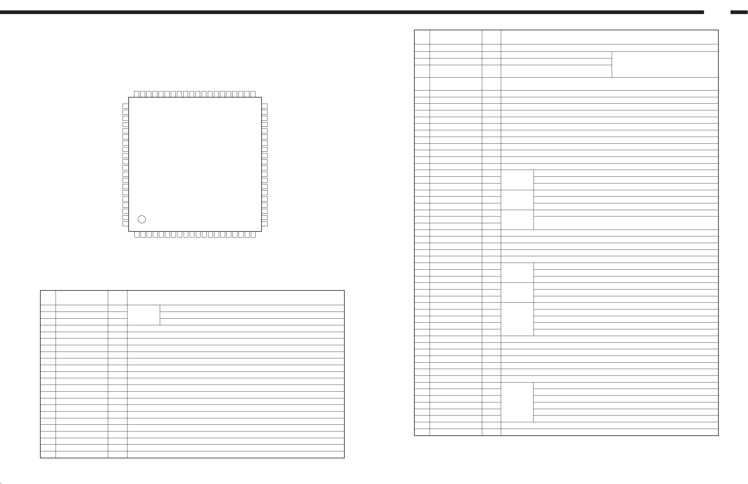
LC78645E (IC204)
DATA
DATACK
LRSY
ASDFIN
ASDACK
ASLRCK
16MOUT
EFLG
C2F
XVSS
FSX/16MIN
XIN
XOUT
XVDD
RVDD
60595857565554535251504948474645444342
61
CE
62
CL
63
DI
64
DO
65
∗WRQ
∗RES
66
DRF
67
VDD5
68
69
VSS
CONT3
CONT2
CONTI
PDOI
PDO2
VVSS
PCKIST
VVDD
FR
LDS
LDD
70
71
72
73
74
75
76
77
78
79
80
123456789
SLCO
EFMIN
SLCIST
RF
TOP VIEW
FIN1
RFVSS
RFVDD
1011121314151617181920
FE
TE
FIN2
TIN1
TIN2
REFI
VREF
TEC
LC78645E Terminal Function
Pin
No.
Symbol
1 SLCO O Control output
2 SLCIST AI R con. pin for current setting of SLCO
3 EFMIN I RF sig. input pin
I/O
For slice
level control
4 RF AO RF sig. monitor pin
5 RFVDD Power pin for RF
6 RFVSS GND pin for RF, connect to 0V
7 FIN1 AI A+C sig. input pin
8 FIN2 AI B+D sig. input pin
9 TIN1 AI E sig. input pin
10 TIN2 AI F sig. input pin
11 VREF AO Vref volt output pin
12 REFI AI Vref volt setting pin
13 FE AO FE sig. monitor pin
14 TEC AO LPF cap. for TE sig. connect pin
15 TE AO TE sig. monitor pin
16 REMON AO RF internal sig. monitor pin
17 JITTC A Cap. connect pin for jitter detect
18 ADAVDD Power pin for servo A/D & D/A
19 ADAVSS GND pin for servo A/D & D/A, connect to 0V
20 TDO AO Output pin for tracking control, D/A output
21 FDO AO Output pin for focus control, D/A output
22 SPDO AO Output pin for spindle control, D/A output
23 SLDO AO Output pin for sled control, D/A output
Function
RCHO
RVSS
JITTC
RFMON
LVS S
ADAVDD
LCHO
LVDD
41
TDO
ADAVSS
40
TEST
39
DOUT
38
VDD
37
(3.3V) VSS
36
MONI5
MONI4
35
MONI3
34
MONI2
33
32
MONI1
FSEQ
31
30
V/∗P
DEFECT
29
28
SBCK/FG
27
SBCK/CONT6
26
CONT5
25
CONT4
24
GPDAC
23
SLDO
22
SPDO
21
FDO
Pin
No.
Symbol
I/O
Function
24 GPDAC AO Servo D/A general output pin
25 CONT4 I/O General output pin 4
26 CONT5 I/O General output pin 5
27 SBCK/CONT6 I/O
28 SBCK/FG I
General output pin 6
or sub-code read out clock input pin
Sub-code read out clock input pin / FG sig. input pin / External emphasis set pin
Function decided by command, connect to 0V when not in use
Control from µcom command, connect to 0V
or open when not in use
29 DEFECT O Defect pin
30 V/*P O Auto switching monitor output pin of rough/phase servo control, H: Rough, L: Phase
31 FSEQ O Sync sig. detect output pin, H: When sync sig. of detected EFM and external are equal
32 MONI1 O Internal sig. monitor pin 1
33 MONI2 O Internal sig. monitor pin 2
34 MONI3 O Internal sig. monitor pin 3
35 MONI4 O Internal sig. monitor pin 4
36 MONI5 O Internal sig. monitor pin 5
37 VSS Digital block GND pin, connect to 0V
38 VDD Digital block power pin
39 DOUT O Digital OUT pin (EIAJ format)
40 TEST I Input pin for test, connect to 0V
41 LVDD Power pin for Lch
42 LCHO AO Output pin for Lch
43 LVSS GND pin for Lch, connect to 0V
44 RVSS GND pin for Rch, connect to 0V
45 RCHO AO Output pin for Rch
Lch D/A
converter
Rch D/A
converter
46 RVDD Power pin for Rch
47 XVDD Power pin for x’tal osc.
48 XOUT O
49 XIN I
For x’tal osc.
33.8688MHz x’tal resonater connect pin
50 FSX/16MIN I/O 7.35kHz sync sig. output pin or external clock input pin for DF, DAC
51 XVSS GND pin for x’tal osc., connect to 0V
52 C2F O C2 flag output pin
53 EFLG O Correction monitor pin of C1, C2
54 16MOUT O 16.9344MHz output pin
55 ASLRCK I L/R clock input pin (connect to 0V when not in use)
56 ASDACK I Bit clock input pin (connect to 0V when not in use)
57 ASDFIN I L/Rch data input pin (connect to 0V when not in use)
58 LRSY O L/R clock output pin
59 DATACK O Bit clock output pin
60 DATA O L/Rch data output pin
For anti-
shock mode
For digital
data output
61 CE I Chip enable sig. input pin
62 CL I Data transfer clock input pin
63 DI I Data input pin
For µcom I/F
64 DO O Data output pin (Nch open drain output)
65 *WRQ O Interrupt sig. output pin
66 *RES I Reset input pin, set to “L” once when power ON
67 DRF O Focus ON detect pin
68 VDD5 Power pin for µcom I/F
69 VSS Digital block GND pin, connect to 0V
70 CONT3 I/O General output pin 3
71 CONT2 I/O General output pin 2
72 CONT1 I/O General output pin 1
73 PDO1 O Phase compare out pin 1 for built-in VCO control
74 PDO2 O Phase compare out pin 2 for built-in VCO control
75 VVSS GND pin for built-in VCO control
76 PCKIST AI R con. pin for PDO1, 2 output current setting
For PLL
77 VVDD Power pin for built-in VCO control
78 FR AI R con. pin for built-in VCO frequency range setting
79 LDS AI Laser power detect sig. input pin
80 LDD AO Laser power control sig. output pin
41
25
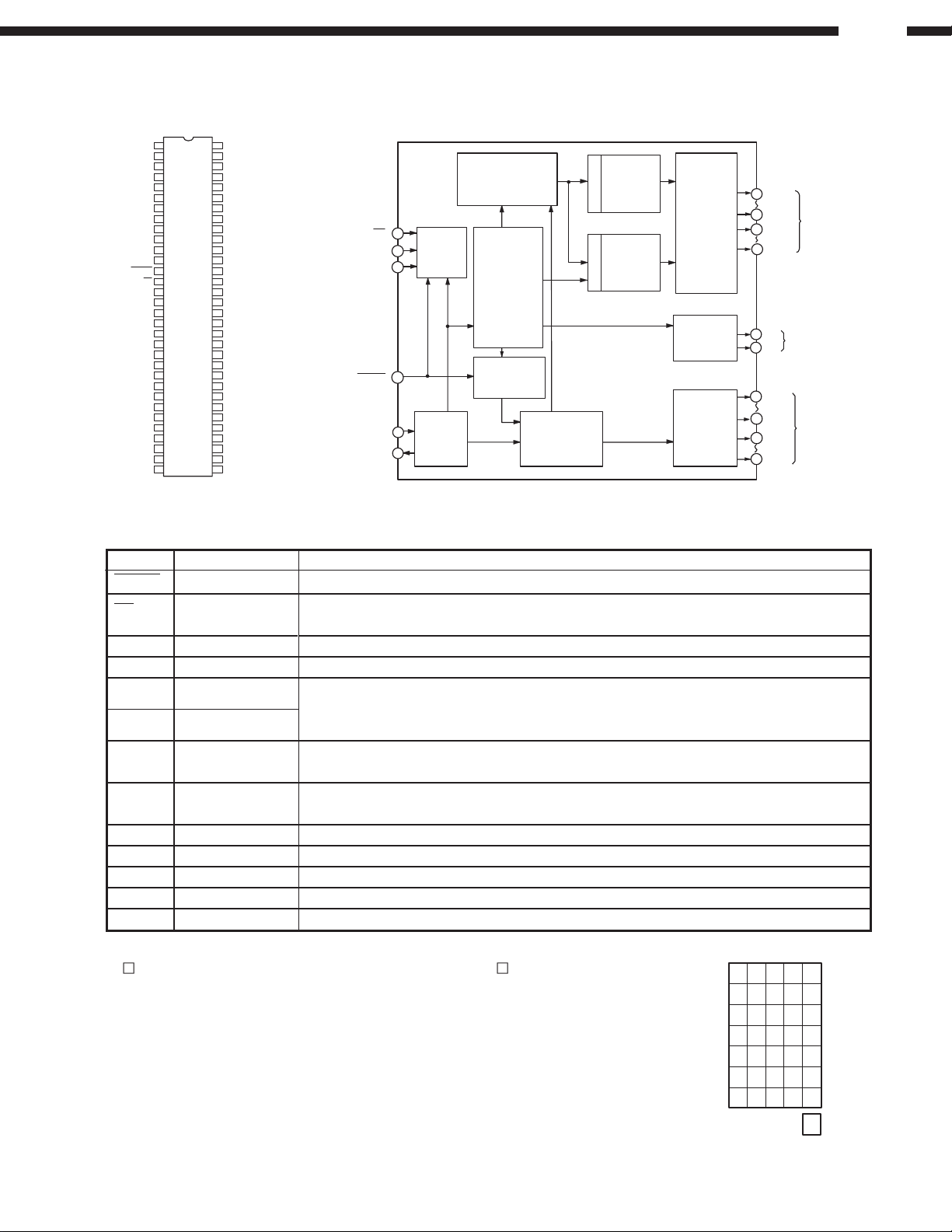
M66004FP (IC701)
DIG
11
1
2
DIG
10
3
DIG
09
DIG
08
4
DIG
07
5
DIG
06
6
DIG
05
7
DIG
04
8
9
DIG
03
DIG
02
10
DIG
01
11
DIG
00
12
13
RESET
CS
14
15
SCK
SDATA
16
PI
17
PO
18
19
Vcc1
20
X
out
21
X
in
22
Vss
SEG
23
35
24
SEG
34
SEG
33
25
SEG
32
26
SEG
31
27
28
SEG
30
SEG
29
29
SEG
28
30
SEG
27
31
Vp SEG
32
DIG
64
63
DIG
62
DIG
DIG
61
60
Vcc2
59
SEG
SEG
58
SEG
57
56
SEG
55
SEG
54
SEG
53
SEG
52
SEG
51
SEG
50
SEG
49
SEG
48
SEG
47
SEG
46
SEG
45
SEG
SEG
44
43
SEG
42
SEG
41
SEG
SEG
40
39
SEG
38
SEG
SEG
37
SEG
36
35
SEG
34
SEG
33
12
13
14
15
00
01
02
03
04
05
06
07
08
09
10
11
12
13
14
15
16
17
18
19
20
21
22
23
24
25
26
C hip Select Input
S h ift C lo c k In p u t
S e r ia l D a ta In p u t
R e s e t In p u t
C lo c k In p u t
C lock O u tput
CS
SCK
SDATA
RESET
XIN
XOU T
14
15
16
13
21
20
Serial
Reception
Circuit
Clock
G eneration
Circuit
D isplay C ode R eg ister
(8 -b it x 1 6 )
code
write
C o d e /
C om m and
Control Circuit
Display Control
R egister
D is p la y C o n t ro lle r
RAM
write
code select
CGROM
(35-bit x 160)
DecoderDecoder
CGROM
(35-bit x 16)
Segm ent
O utput
Circuit
O u tp u t P o rt
(2 -bit)
D igit O utput
Circuit
D-107
SEG
00
59
26
SEG
33
31
23
18
17
12
1
64
61
SEG
SEG
P0
P1
DIG
DIG
DIG
DIG
Segm ent
27
O utput
35
O u tp u t P o rt
00
11
D igit O utput
12
15
M66004FP Terminal Function
Symbol Name Function
RESET Reset Input
CS Chip Select Input
SCK Shift Clock Input
SDATA Serial Data Input
X
IN Clock Input
OUT Clock Output
X
DIG 00~
DIG 15
SEG 00~
SEG 35
Digit Output
Segment Output
P0, P1
VCC1
VCC2
Vss
Vp
(Forwarding connection of segment output terminal.)
in the right figure indicates 1 dot of segment, the figure in shows the segment output
terminal number (00~35) to be connected.
Initialzes internal state of M66004.
Able to communicate with MCU in "L" mode.
Command from MCU will be disregareded in "H" mode.
Shifts input data at rise from "L" to "H".
Inputs character code or command data needed to display from MSB.
Sets oscillation frquency by connecting external resistor and capacitor (maximum
oscillation frequency fosc (max)=1MHz). Also feasible to apply external clock. In this case,
inject external clock to Xin terminal and open Xout terminal.
Connect to digit terminal of VFD. DIG00~DIG15 correspond to the 1st figure to 16th figure
respectively.
Connect to segment terminal of VFD. For corresponding SEG00~SEG35 to segment
terminal of VFD, refer to the figure right.
Output port (static operation).
Positive power supply terminal for internal logic.
Positive power supply terminal for high tension output port.
GND terminal.
Negative power supply terminal for VFD drive.
00 01 02 03 04
05 06 07 08 09
10 11 12 13 14
15 16 17 18 19
20 21 22 23 24
25 26 27 28 29
30 31 32 33 34
35
26
D-107
)
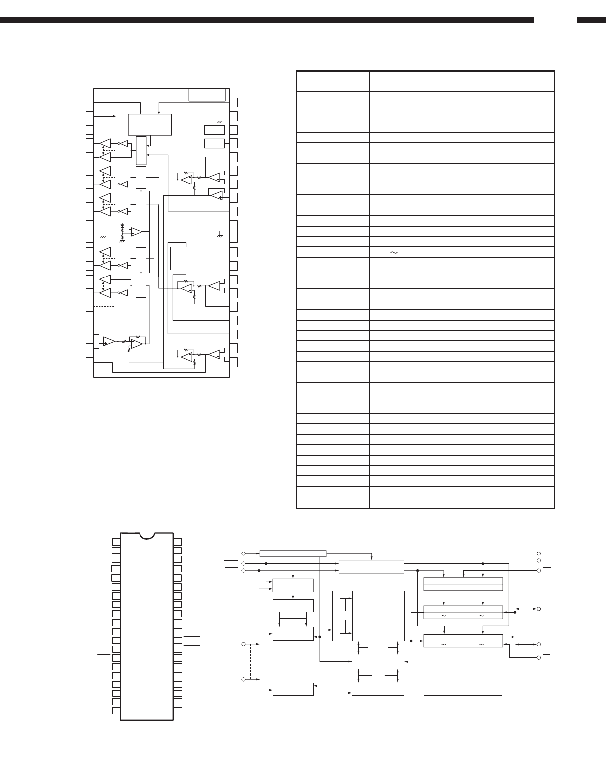
LA6559 (IC201)
1
REV
Signal System VCC
2
S-VCC
VCC2
VLO-
VLO+
VO4+
VO4-
VO3+
VO3-
VO2+
VO2-
VO1+
VO1-
VCC1
VIN1
VIN1-
VIN1+
VIN2
FR
3
4
5
6
7
8
9
Power
System
GND
FR
10
11
12
13
14
15
16
17
18
Power Supply
(LOADING)
(Forward/Reverse/
Power Supply
(CH1 to CH4)
11k
LC32V4265T-25
(IC208)
Input
Break/OFF)
Control
Output
Level
Shift
Level
Shift
Level
Shift
Level
Shift
33k
Signal System GND
CH2 to CH4
Output
CH1 Output
ON/OFF
33k
Power System GND
3.3VREG
(External PNP)
33k
3.3VREG GND
3.3VREG
Power Supply
33k
Thermal
Shutdown
MUTE2
MUTE1
11k
PNP Tr
Collector
11k
11k
PNP Tr
Base
36
FWD
35
S-GND
34
MUTE2
33
MUTE1
32
VIN4
31
VIN4-
30
VIN4+
29
VREF-IN
28
VCONT(LOADING
FR
FR
27
REG-OUT
26
REG-IN
25
VIN3+
24
VIN3-
23
VIN3
22
GND-VREG
21
VCC-VREG
20
VIN2+
19
VIN2-
Pin
No.
Name
1 REV
2 S-Vcc
Function
5CH output change terminal, logic input of
loading block
signal system power supply
(BTL-AMP:CH1~4)
3 Vcc2 Power supply for loading block
4 VL0− Loading output (−)
5 VL0+ Loading output (+)
6 VO4+ Output terminal (+) for channel 4
7 VO4− Output terminal (−) for channel 4
8 VO3+ Output terminal (+) for channel 3
9 VO3− Output terminal (−) for channel 3
10 VO2+ Output terminal (+) for channel 2
11 VO2− Output terminal (−) for channel 2
12 VO1+ Output terminal (+) for channel 1
13 VO1− Output terminal (−) for channel 1
14 Vcc1 CH1 CH4(BTL-AMP) output stage power supply
15 VIN1 Input terminal for channel 1
16 VIN1− OP-AMP input AMP-A input terminal (−)
17 VIN1+ OP-AMP input AMP-A input terminal (+)
18 VIN2 Input terminal for channel 2, input AMP output
19 VIN2− Input terminal (−) for channel 2
20 VIN2+ Input terminal (+) for channel 2
21 Vcc-VREG 3.3VREG power supply
22 GND-VREG 3.3VREG GND
23 VIN3 Input terminal for channel 3, input AMP output
24 VIN3− Input terminal (−) for channel 3
25 VIN3+ Input terminal (+) for channel 3
26 REG-IN PNP transistor base connected
27 REG-OUT
3.3V power output to which the PNP transistor
collector connected
28 VCONT Loading output voltage set terminal
29 VREF-IN Reference voltage applied terminal
30 VIN4+ Input terminal (+) for channel 4
31 VIN4- Input terminal (−) for channel 4
32 VIN4 Input terminal for channel 4, input AMP output
33 MUTE1 Output ON/OFF for channel 1 (BTL AMP)
34 MUTE2 Output ON/OFF for channel 2 to 4 (BTL AMP)
35 S-GND Signal system GND
36 FWD
Output change terminal (FWD) for loading
output (VLO+−), logic input of loading block
V
1
CC
2
I/O1
3
I/O2
4
I/O3
5
I/O4
6
V
CC
7
I/O5
8
I/O6
9
I/O7
TOP VIEW
10
I/O8
11 30
N.C.
12 29
N.C.
13 28
WE
14 27
RAS
15 26
N.C.
16 25
A0
17 24
A1
18 23
A2
19 22
A3
20
V
CC
40
VSS
39
I/O16
38
I/O15
37
I/O14
36
I/O13
35
V
SS
34
I/O12
33
I/O11
32
I/O10
31
I/O9
RAS Vcc
UCAS
LCAS
N.C.
LCAS
UCAS
A0
OE
A8
A7
A6
A8
A5
Clock Generator No.1
Mode Control
Refresh Counter
Row Address
Buffer
Column Address
Buffer
Clock Generator No.2
Row Decoder
262144 Memory Cell
512
Column Decoder
x16 Bit
512x16
Sense Amp
I/O Gate
512
Pre-Decoder
Clock Generator No.3
Lower Byte Upper Byte
Data Input Buffer
I/O1
I/O8 I/O9 I/O16
Data Output Buffer
I/O1
I/O8 I/O9 I/O16
PWB Bias Generator
Vss
WE
I/O1
I/O16
OE
A4
V
SS21
27
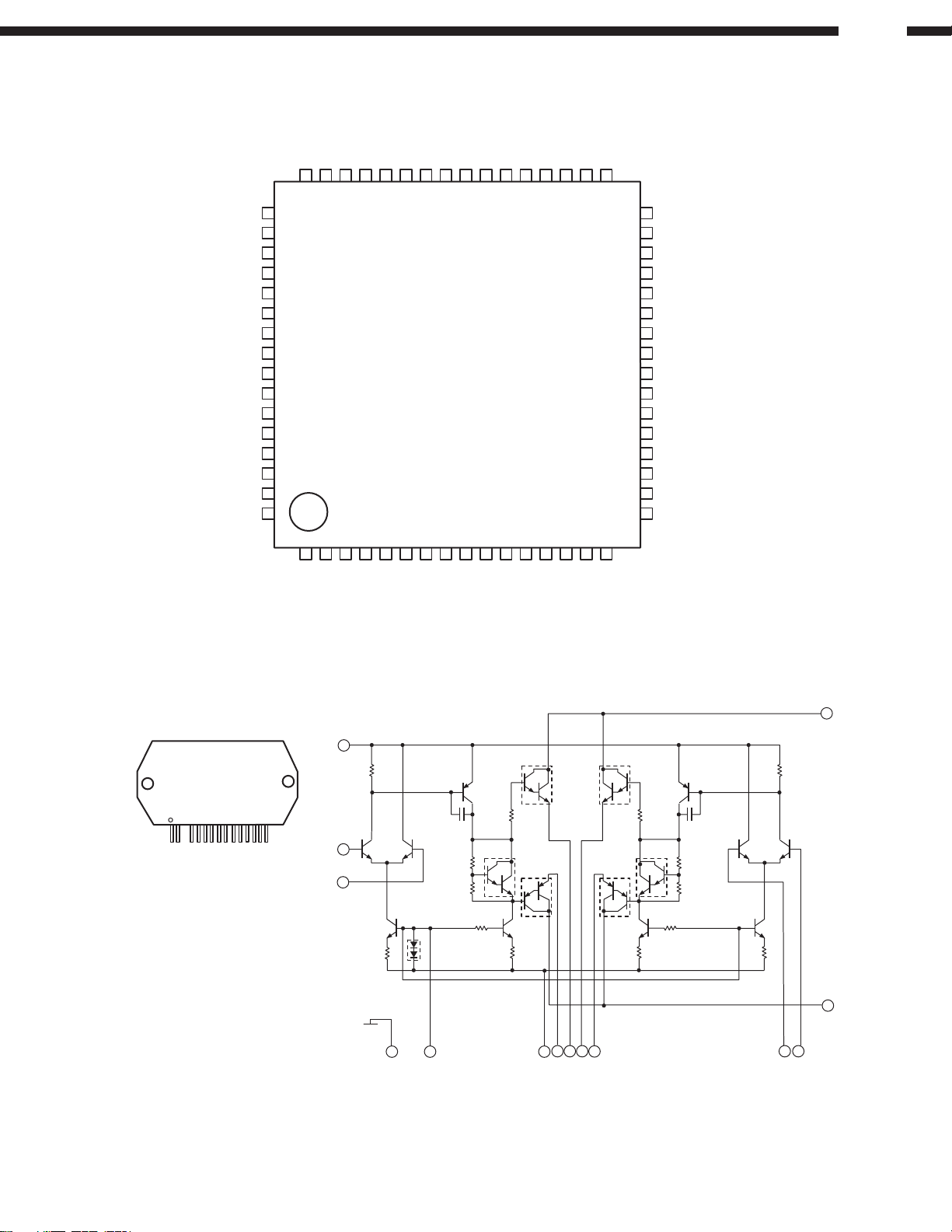
LC75396NE (IC305)
LTIN
LF1C1
LF1C2
LF1C3
LF2C1
LF2C2
LF2C3
LF3C1
LF3C2
LF3C3
LF4C1
LF4C2
LF4C3
LF5
LTOUT
48 47 46 45 44 43 42 41 40 39 38 37 36 35 34 33
D-107
LFIN
LSELO
LINVIN1
V
R1
R2
R3
R4
R5
RINVIN1
RSELO
RTIN
LFCOM
RFCOM
32
31
30
29
28
27
26
25
24
23
22
21
20
19
18
17
LFOUT
LRIN
LRCOM
LROUT
LVref
SS
V
CE
DI
CL
Vref
RVref
RROUT
RRCOM
RRIN
RFOUT
49
50
L5
51
L4
52
L3
53
L2
54
L1
55
DD
56
57
58
59
60
61
62
63
64
1
34
RF1C12RF1C2
RF1C35RF2C1
TOP VIEW
67
RF2C2
RF2C3
89
RF3C1
RF3C2
10 11 12 13 14 15 16
RF5
RF3C3
RF3C1
RF3C2
RF3C3
RTOUT
RFIN
STK402-050 (SW: IC500, 700)
FRONT VIEW
1
15
4
R1
1
TR1 TR2
2
TR3
R2
SUB
8
TR7
TR4
C1
R3
R4
D1
13
5
R6
TR5
TR8
TR6
R5
R7
7610
12
TR9
TR11
R8
C2
TR14
TR12
TR13
R9
R11
R12
R10
TR10
11
R13
TR15
TR16
R14
9
14 15
28
D-107
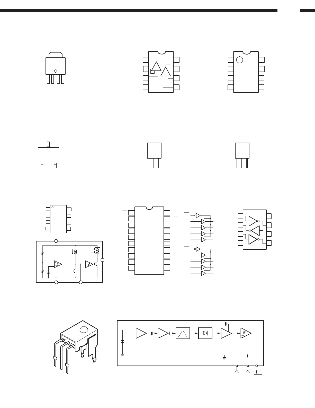
BA033S (IC207) BA6417F (IC202)
BA15218F
(IC301, 303, 401)
(SW: IC101, 102, 105, 106, 401 )
3
1
245
1.CTL
2.Vcc
3.GND
4.OUT
5.N. C.
MN13821C (IC102)
VDD
TOP
VIEW
OUT Vss
NJM7806FA(S) (IC501)
1
1ch
−
+
2
IN1
3
+IN1
45
V
EE
+
2ch
8 OUT1
7
−
6
(SW: IC202, 203)
FRONT
VIEW
GND
Input
Output
Vcc
OUT2
IN2
+IN2
1
2
VM
3
Vcc
45
FIN
NJM7812FA(S) (SW: IC201)
FRONT
VIEW
GND
Input
Output
8 OUT1
7
6
GND
OUT2
VRFF
RIN
M51953AFP (IC103)
NC NC
1
NC
2
3
NC
GND
4
R1
R2
1.25V
Vcc
GND
7
4
8
Vcc
7
OUTPUT
6
DELAY-CAP
5
A
5µ
Typ Typ
DELAY-CAP
25µ
A
5
SN74LVC244APW (IC205)
6
OUTPUT
GP1U271X (Remote Control Sensor)
1OE
1A1
2Y4
1A2
2Y3
1A3
2Y2
1A4
GND
GND
10
TC7WU04F
Vcc
Limiter
Amp
20
19
18
17
16
15
14
13
12
11
1OE
2OE
1A1
1Y1
1A2
2A4
1A3
1Y2
1A4
2A3
2OE
1Y3
2A1
2A2
2A2
1Y4
2A3
2A1
2A4
BPF Integrator
Detector &
Comparator
1Y1
1Y2
1Y3
1Y4
2Y1
2Y2
2Y3
2Y4
1A
3Y
2A
GND
1
2
3
4
5
6
7
8
9
Head
Amp
(IC206)
1
2
3
4
Hysteresis
Comparator
8
Vcc
7
1Y
6
3A
5
2Y
V
OUT
Vcc
GND
GND Vcc
Vout
29
 Loading...