

Page 1
INTEGRATED NETWORK AV RECEIVER
AVR-X6400H
Service Manual
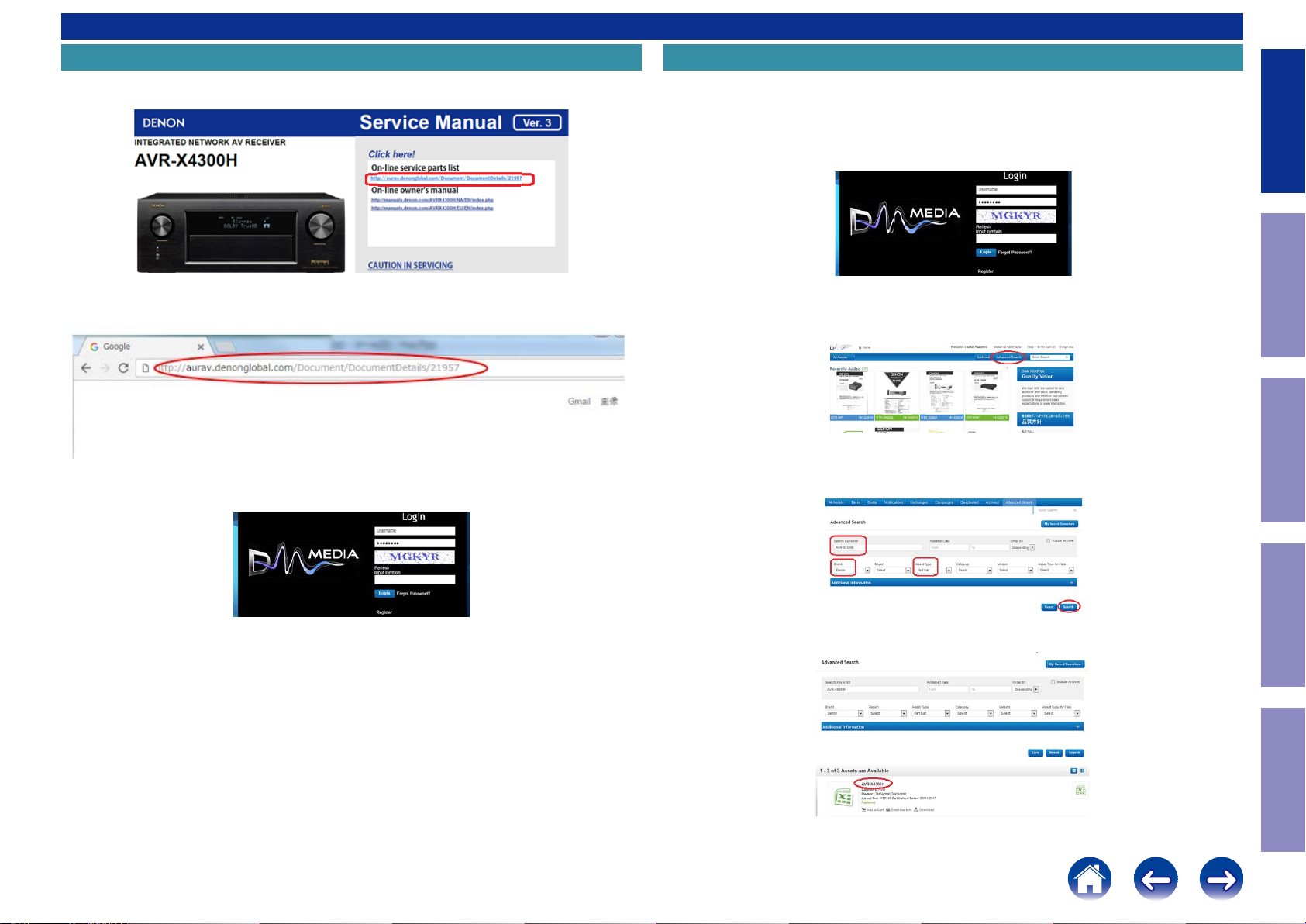
Click here!
On-line service parts list
http://dmedia.dmglobal.com/Document/DocumentDetails/23542
Online Parts List (P5 to P7)
WEB owner’s manual (Release schedule)
http://manuals.denon.com/AVRX6400H/NA/EN/index.php (July 2017)
http://manuals.denon.com/AVRX6400H/EU/EN/index.php (July 2017)
http://manuals.denon.com/AVRX6400H/AP/ZH/index.php (September 2017)
CAUTION IN SERVICING
ELECTRICAL
Ver. 1
MECHANICAL
REPAIR INFORMATION
UPDATING
•Forpurposesofimprovement,specicationsanddesignaresubjecttochangewithoutnotice.
•Pleaseusethisservicemanualwithreferringtotheoperatinginstructionswithoutfail.
•Someillustrationsusinginthisservicemanualareslightlydifferentfromtheactualset.
START::|sX3k6VQNaf/6VbQg1Aav9Q==|NtOOpK8Hw7SVyAFQuznArZMqgzToOuTqeouhB6NC5/c=|XOIUVeyoWOE5XcWqSdEcbA==|::END
Page 2
CAUTION IN SERVICING
SAFETY PRECAUTIONS
NOTE FOR SCHEMATIC DIAGRAM
NOTE FOR PARTS LIST
INSTRUCTIONS FOR HANDLING SEMICONDUCTORS AND OPTICAL UNIT
Online Parts List
Accessing the Parts List
Logging in to New SDI and Accessing the Parts List
Accessing the Part List from the Model Asset Screen
PRINTED CIRCUIT BOARDS Parts Table
Downloading the Parts List as an Excel File
Revision History
Searching Part Numbers or Ref. Numbers
Caution in
servicing
Electrical Mechanical Repair Information Updating
CAUTION IN SERVICING.
Initializing This Unit
JIG FOR SERVICING
2
Page 3
SAFETY PRECAUTIONS
The following items should be checked for continued protection of the customer and the service
technician.
Leakage current check
Before returning the set to the customer, be sure to carry out either (1) a leakage current check or
(2) a line to chassis resistance check. If the leakage current exceeds 0.5 milliamps, or if the resistance
from chassis to either side of the power cord is less than 460 kohms, the set is defective.
Be sure to test for leakage current with the AC plug in both polarities, in addition, when the set's
power is in each state (on, off and standby mode), if applicable.
◎ Make a safety check after servicing!
Check that all screws, parts and wires removed or disconnected when servicing have been put back
in their original positions, check that no serviced parts have deteriorate the area around. Then make
an insulation check on the external metal connectors and between the blades of the power plug, and
otherwise check that safety is ensured.
(Insulation check procedure)
Unplug the power cord from the power outlet, disconnect the antenna, plugs, etc., and on the power.
Using a 500V insulation resistance tester, check that the insulation resistance value between the inplug
and the externally exposed metal parts (antenna terminal, headphones terminal, input terminal, etc.) is
1M Ω or greater. If it is less, the set must be inspected and repaired.
Caution in
servicing
Electrical Mechanical Repair Information Updating
CAUTION
Please heed the following cautions and instructions during servic-
ing and inspection.
◎ Heed the cautions!
Cautions which are delicate in particular for servicing are labeled on the cabinets, the parts and the
chassis, etc. Be sure to heed these cautions and the cautions described in the handling instructions.
◎ Cautions concerning electric shock!
(1) An AC voltage is impressed on this set, so if you touch internal metal parts when the set is energized,
you may get an electric shock. Avoid getting an electric shock, by using an isolating transformer and
wearing gloves when servicing while the set is energized, or by unplugging the power cord when
replacing parts, for example.
(2) There are high voltage parts inside. Handle with extra care when the set is energized.
◎ Caution concerning disassembly and assembly!
Through great care is taken when parts were manufactured from sheet metal, there may be burrs on the
edges of parts. The burrs could cause injury if ngers are moved across them in some rare cases. Wear
gloves to protect your hands.
◎ Use only designated parts!
The set's parts have specic safety properties (re resistance, voltage resistance, etc.). Be sure to use
parts which have the same properties for replacement. The burrs have the same properties. In particular,
for the important safety parts that are indicated by the z mark on schematic diagrams and parts lists,
be sure to use the designated parts.
◎ Be sure to mount parts and arrange the wires as they were originally placed!
For safety seasons, some parts use tapes, tubes or other insulating materials, and some parts are mounted away from the surface of printed circuit boards. Care is also taken with the positions of the wires by
arranging them and using clamps to keep them away from heating and high voltage parts, so be sure to
set everything back as it was originally placed.
CAUTION
Many of the electric and the structural parts used in the set have special safety properties. In most cases
these properties are difcult to distinguish by sight, and the use of replacement parts with higher ratings (rated power and withstand voltage) does not necessarily guarantee that safety performance will
be preserved. Parts with safety properties are indicated as shown below on the wiring diagrams and the
parts list in this service manual. Be sure to replace them with the parts which have the designated part
number.
(1) Schematic diagrams Indicated by the z mark.
(2) Parts lists Indicated by the z mark.
The use of parts other than the designated parts could cause electric shocks, res or other dangerous
situations.
Concerning important safety parts
3
Page 4
NOTE FOR SCHEMATIC DIAGRAM
WARNING:
Parts indicated by the z mark have critical characteristics. Use ONLY replacement parts recommended
by the manufacturer.
CAUTION:
Before returning the set to the customer, be sure to carry out either (1) a leakage current check or (2)
a line to chassis resistance check. If the leakage current exceeds 0.5 milliamps, or if the resistance from
chassis to either side of the power cord is less than 460 kohms, the set is defective.
WARNING:
DO NOT return the set to the customer unless the problem is identied and remedied.
NOTICE:
ALL RESISTANCE VALUES IN OHM. k=1,000 OHM / M=1,000,000 OHM
ALL CAPACITANCE VALUES ARE EXPRESSED IN MICRO FARAD, UNLESS OTHERWISE INDICATED. P
INDICATES MICRO-MICRO FARAD. N INDICATES NANO FARAD. EACH VOLTAGE AND CURRENT ARE
MEASURED AT NO SIGNAL INPUT CONDITION. CIRCUIT AND PARTS ARE SUBJECT TO CHANGE WITHOUT
PRIOR NOTICE.
NOTE FOR PARTS LIST
1. Parts indicated by "
2. When ordering a part, make a clear distinction between "1" and "I" (i) to avoid mis-supplying.
3. A part ordered without specifying its part number can not be supplied.
4. Part indicated by "@" mark is not illustrated in the exploded view.
WARNING: Parts indicated by the z mark have critical characteristics. Use ONLY replacement parts
recommended by the manufacturer.
nsp
" on this table cannot be supplied.
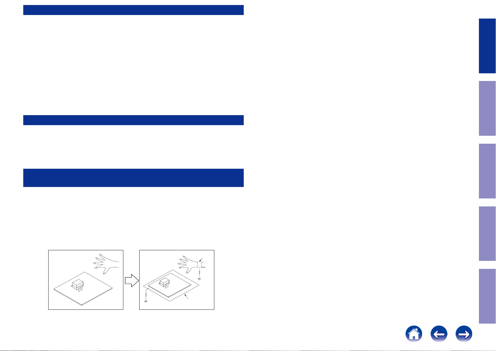
INSTRUCTIONS FOR HANDLING SEMICONDUCTORS AND
OPTICAL UNIT
Electrostatic breakdown of the semi-conductors or optical pickup may occur due to a potential difference caused by electrostatic charge during unpacking or repair work.
1. Ground for Human Body
Be sure to wear a grounding band (1 M ohm) that is properly grounded to remove any static electricity
that may be charged on the body.
2. Ground for Workbench
Be sure to place a conductive sheet or copper plate with proper grounding (1 M ohm) on the workbench or other surface, where the semi-conductors are to be placed. Because the static electricity
charge on clothing will not escape through the body grounding band, be careful to avoid contacting
semi-conductors with your clothing
<Incorrect>
<Correct>
Grounding Band
Caution in
servicing
Electrical Mechanical Repair Information Updating
CBA
1MΩ
CBA
Conductive Sheet or
Copper Plate
1MΩ
4
Page 5
Online Parts List
Accessing the Parts List Logging in to New SDI and Accessing the Parts List
(1) Click the URL link on the cover of the service manual.
Examples of display
NOTE : If the web browser does not open automatically, copy the URL and paste it into the address bar
of the web browser and then press Enter.
(1) Access New SDI from the URL below.
<http://dmedia.dmglobal.com>
(2) When the login screen is displayed, enter your username and password.
(3) Enter the 5 letters shown as the blue CAPTCHA code as single-byte characters.
If the text is unclear, click "Refresh" to change the CAPTCHA code, and enter it again.
(4) Press the "Login" button.
(5) When the Home screen is displayed, click "Advanced Search".
Caution in
servicing
Electrical Mechanical Repair Information Updating
(2) When the login screen is displayed, enter your username and password.
(3) Enter the 5 letters shown as the blue CAPTCHA code as single-byte characters.
If the text is unclear, click "Refresh" to change the CAPTCHA code, and enter it again.
(4) Press the "Login" button.
(6) Enter the following search conditions and click "Search".
Keyword : Model name Brand : brand name Asset Type : Part list
(7) Click the model name when the search results are displayed.
5
Page 6
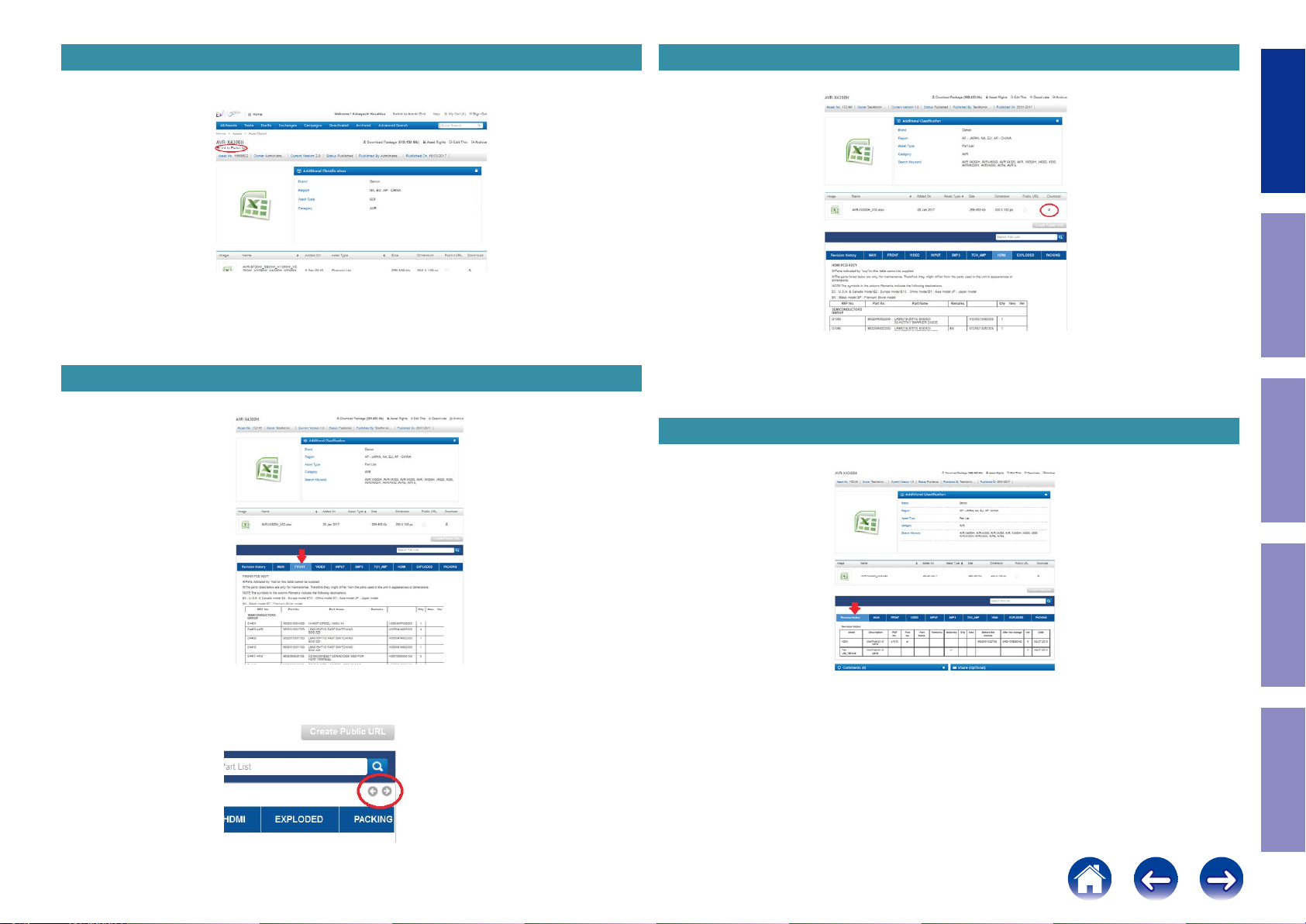
Accessing the Part List from the Model Asset Screen
(1) Display Model Asset from New SDI.
(2) Click the section displayed as ▼ Link to Part Lists under the model name.
NOTE : If the ▼ Link to Parts List section is not displayed, download the parts table from the Asset list.
PRINTED CIRCUIT BOARDS Parts Table
(1) Display the Parts List. Click the PCB name in the blue bar to display the parts list for the board.
Downloading the Parts List as an Excel File
(1) Displays the Parts List. Click the Download icon.
Revision History
(1) Click "Revision history" in the blue bar.
Caution in
servicing
Electrical Mechanical Repair Information Updating
Left and right arrow icons are displayed if the circuit board name does not t in the blue bar.
Click these icons to display a different part of the name when necessary.
← Icons to move the circuit board name
left and right in the blue bar
The following details are displayed.
Sheet : Name of the changed sheet
Description : Description of the changes
Remarks : Destination, color information
Factories : Factory number
Ver : Version number after revision if changes were made to the parts list
Date : Date of changes
6
Page 7
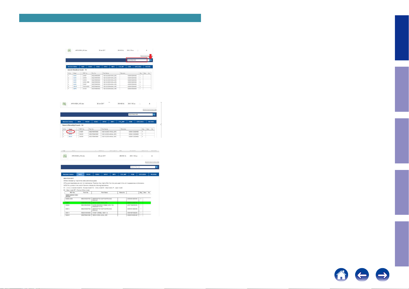
Searching Part Numbers or Ref. Numbers
You can search a Parts List for part numbers or Ref. numbers.
(1) Enter the part number or Ref. number in the search window of the Parts List, and press the search
button.
(2) The search results are displayed.
The name of the sheet in which the search part is used and the part’s line are displayed.
(3) Next, click the "Sheet" section of the search results.
(4) The Board Part Table opens and the line on which the searched part number appears is highlighted.
Caution in
servicing
Electrical Mechanical Repair Information Updating
7
Page 8
CAUTION IN SERVICING.
Initializing This Unit
Make sure to initialize this unit after replacing the microcomputer or any peripheral equipment, or the
digital PCB.
1. Press the power button to turn off the power.
2. While holding down buttons "CURSOR d" and "CURSOR f" simultaneously, press the power button to
turn on the power.
3. Release the buttons after conrming that the display ashes at 1-second intervals.
* The unit is initialized.
Use network initialization mode to initialize the network related settings.
Caution in
servicing
NOTE: • If the unit fails to enter the service mode in step 3, repeat the procedure from step 1.
• Initializing the device restores the customized settings to the factory settings. Write down
your settings in advance and recongure the settings after initialization.
CURSOR d
CURSOR fX
JIG FOR SERVICING
Use the following jigs (extension cable kit) when repairing the PCBs.
Order with your dealer for the jigs your dealer if necessary.
8U-110084S : EXTENSION UNIT KIT : 1 Set
(See JIG FOR SERVICING)
Electrical Mechanical Repair Information Updating
8
Page 9
ELECTRICAL
SCHEMATIC DIAGRAMS
SCH01_DIGITAL CONNECT
SCH02_MAIN CPU
SCH03_EXPANDER
SCH04_AUDIO PLD
SCH05_DIR DA SUPPLY
SCH06_ADI DSP1
SCH07_ADI DSP2
SCH08_ADI DSP3
SCH09_ADI DSP4
SCH10_HDMI SUPPLY
SCH11_DECODER
SCH12_HDMI SW2
SCH13_HDMI SW1
SCH14_IP OSD
SCH15_IP OSD DDR
SCH16_VIDEO PLD
SCH17_HDMI TX
SCH18_E ARC
SCH19_NET MODULE CONNECT
SCH20_AUDIO/VIDEO CONNECT
SCH21_AUDIO VOLUME
SCH22_PREOUT
SCH23_VIDEO SELECTOR
SCH24_CONNECT
SCH25_AMP CONNECT
SCH26_ZONEDAC ADC
SCH27_MAIN DAC
SCH28_FRONT HDMI USB
SCH29_SMPS
SCH30_232C PHONO
SCH31_P.AMP1
SCH32_P.AMP2
SCH33_SPEAKER
SCH34_REG
SCH35_FLD
PRINTED CIRCUIT BOARDS
DIGITAL
AUDIO VIDEO, FRONT HDMI USB, CONNECT-1,
CONNECT-2, CONNECT-4
DAC, L AMP CONNECT, R AMP CONNECT, FRONT
SPEAKER, HEIGHT2 SP, HP, P.SW, CONNECT-3
AMP1, AMP2, SMPS, 232C PHONO, POSISTER,
RADIATOR COVER
LEVEL DIAGRAM
FRONT ch
CENTER / SURROUND ch
SUBWOOFER ch
SURROUND BACK / HEIGHT1 / HEIGHT2 ch
ZONE2 / ZONE3 ch
BLOCK DIAGRAM
ANALOG AUDIO DIAGRAM
DIGITAL AUDIO DIAGRAM
VIDEO DIAGRAM
POWER DIAGRAM
SEMICONDUCTORS
1. IC's
2. FL DISPLAY
3. Remote Code Table
Caution in
servicing
Electrical Mechanical Repair Information Updating
9
Page 10
SCHEMATIC DIAGRAMS
SCH01_DIGITAL CONNECT
N6012
N6012
33P-SOCKET(C125Z2)
33
A-7V
A+7V
DGND
M3.3V
DA3.3V
TO N5907
TO FRONT CONNECT
TRDET
TRIG12V
TRIGGND
TEHRMALE
THERMALF
AMPSIGDET
FANDET_ON
CURRENTDET
All Ref.No. has been described in the parts list are four digits.
But there are less than four digits of printed Ref.No. on the PCB, and they have become four digits after the header by adding "0" in the parts list.
To_8U-210228-6(N5907)
1011121314151617181920212223242526272829303132
DGND
DGND
TUSCL
TUSEN
TUSDA
TURST
DCDET
TUGPIO
FANDET_HIGH
ASODET
AEXP_STB
AEXP_CLK
AEXP_DATA
AEXP_OE
CONNECT-1_UNIT
DGND
DA+5V
DACGND
ZADINL....
ZADINR....
123456789
Z2VCOM
N6011
N6011
33P-FFC
123456789
DGND
DA3.3V
Z3DATA
Z3LRCK
Z3MUTE
DA3.3V
TO N5001
TO DAC UNIT
1011121314151617181920212223242526272829303132
DGND
Z2MUTE
Z2LRCK
DGND
DGND
DGND
Z2EMP
Z2BCK
Z2SCK
Z2DATA
ADCDATA
ADCLRCLK
DGND
Z3BCK
DGND
Z3SCK
DGND
Z3EMP
To_8U-210228-2(N5001)
ADCRST
ADCBCK
ADCSCK
DAC_UNIT(1/2)
DAC_RST1
DAC_CCLK
DAC_CCS2
DAC_CCS1
DAC_CDATA
33
DAC_RST2
N6010
33P-FFC
H/PGND
N6010
TO AUDIO/VIDEO UNIT
123456789
MIC
H/PL
H/PR
H/PGND
TO N9018
1011121314151617181920212223242526272829303132
DGND
VAUXR
VAUXL
PREGND
VOL_CLK
ZVOLCLK
SEL_CLK
SEL_DATA
VOL_DATA
ZVOLDATA
DGND
ZVOLSTB
AEXP_CLK
AEXP_STB
To_8U-210228-1(N9018)
A.AUDIO/VIDEO_UNIT(1/4)
DGND
DGND
DV5V
AVSCL
AVSDA
DV3.3V
AEXP_OE
AEXPDATA
DGND
AUX_V
DECIN_V
DECIN_Y
33
DECIN_Cr
DECIN_Cb
100/6.3
OPEN.
C6015
C6024
100/6.3
OPEN
C6017
C6016
0.1
OPEN
C6018
C6019
4.7u
C6020
L6002
L6003
L6004
L6005
L6006
BLM21PG221
BLM21PG221
BLM21PG221
BLM21PG221
0.1
BLM21PG221
C6021
4.7u
OPEN
C6023
C6022
N6001
N6001
7P-EHs
MAINPOWER
D5.2V
D5.2V
DGND
DGND
FB
AC DET
1
2
3
4
5
6
TO SMPS
7
To_8U-110207-7(N6513)
TO N6513
SMPS_UNIT
Caution in
servicing
N6014_
N6005_
N6014
33P-SOCKET(C125Z2)
NETDAC_MCLK
DGND
NETDAC_BCK
DGND
NETDAC_LRCK
NETDAC_DATA
DGND
NETDAC_MUTE
VOLMUTE
CONNECT-3_UNIT
To_8U-110210-11(N5202)
DGND
DAC1_F/FR
DAC1_C/C
DAC1_S/SW1
DGND
DAC1_SW2/SL
DAC1_-/SR
DAC1_-/SW2
DGND
DAC2_-SB/SBR
DAC2_H1/H1L
DAC2_H2/H1R
DGND
DAC2_H3/H2L
TO SIDE CONNECT
DAC2_-/H2R
DGND
DAC1_BCK/CK
DGND
DAC1_MCLK
DGND
DAC1_LRCK/FL
DAC2_LRCK/SBL
DA3.3V
DLHD
TO N5202
TRIG12V
TRIG1
TRIG2
TRIGGND
M3.3V
B/P_IRIN
DGND
232C_Rx
232C_Tx
DGND
REMOTE3.3V
DGND
OPT1
OPT2
DGND
TO DIGITAL IN
COAX2
COAX1
DA3.3V
VS100_IRTX
232C/PHONO_UNIT
To_8U-110207-8(N3903)
TO N3903
1
2
3
4
5
6
7
8
9
10
11
12
13
14
15
16
17
18
19
20
21
22
23
24
25
26
27
28
29
30
31
32
33
19
18
17
16
15
14
13
12
11
10
9
8
7
6
5
4
3
2
1
N6005
19P-FFC
B501
M3-SIDE
9C
TO APLD
TO 8U-310223(4/19)
DLHD
TRIGGER1
TRIGGER2
B/P_IRIN
232O_MI
232I_MO
OPT1
OPT2
COAX2
COAX1
A1
TO 1A
NET MODULE CONNECT
NETDAC_MCLK
NETDAC_BCK
NETDAC_LRCK
NETDAC_DATA
NETDAC_MUTE
VOLMUTE
DAC1_F/FR
DAC1_C/C
DAC1_S/SW1
DAC1_SW2/SL
DAC1_-/SR
DAC1_-/SW2
DAC2_F/FR
DAC2_C/C
DAC2_S/SW1
DAC2_SW2/SL
DAC2_-/SR
DAC1_BCK//CK
DAC1_LRCK/FL
DAC2_LRCK/FL
TO C9
R6005
OPEN
HDMI SUPPLY
DA SUPPLY
A2
A3
TO 2A
TO 3A
DAC input
3
CH1: DACF
CH2: DACLRCK
CH3: DACBCK
CH4: DACMCK
C1937
U1904
1000P
SN74AHCU04PWR
14
VCC
GND
7
1M
R1927
L9100
DGND
A4
DLHD
10/6.3
C9101
Z2DAC_256fs
DLHD
1u
C9103
Z2DAC_64fs
Z2DAC_256fs
R1929
SN74AHCU04PWR
4
SN74AHCU04PWR
2
SN74AHCU04PWR
U9201
1
NC
L2
11
9
PVIN
7
AVIN
6
CE
XCL212B082DR
Z2DAC_fs
Z2DAC_DATA
Z2DAC_MUTE
Z3DAC_64fs
Z3DAC_256fs
Z2DAC_fs
Z2DAC_64fs
Z2DAC_MUTE
Z2DAC_DATA
Z3DAC_256fs
47
NC
L1
LX
LX
FB
GND
Z3DAC_fs
Z3DAC_fs
Z3DAC_64fs
1D
TO D1
BLM21PG221
TO
D5V
TO APLD
TO 4A
98
U1904
SN74AHCU04PWR
11
1312
10
U1904
U1904
SN74AHCU04PWR
3
5
6
U1904
SN74AHCU04PWR
1
U1904
47K
4
R9108
330P
10
0
2
R9109
3
C9116
5
15K
R9110
8
Z3DAC_MUTE
Z3DAC_DATA
MAINADC_fs
MAINADC_DATA
MAINADC_64fs
MAINADC_256fs
Z3DAC_MUTE
Z3DAC_DATA
MAINADC_fs
MAINADC_64fs
MAINADC_DATA
MAINADC_256fs
TO DEC
TO 8U-310223(11/19)
TO 5AA6TO 6A
C1939
1000P
U1904
L9104
BLM21PG221
10/6.3
22/6.3
C9117
C9118
A5
DECIN_Y
DECIN_CR
DECIN_CB
DECIN_Y
DECIN_CR
C1936
0.1
R1931
1.5K
M3.3V
0.01
C9121
C9120 1000P
DECIN_V
Z2DAC_DEMP
DECIN_V
DECIN_CB
AMPSIGDET
0.1
OPEN
C9122
C6004
COAX1
Z3DAC_DEMP
Z2DAC_DEMP
Z3DAC_DEMP
THERMALINF
CURRENTDET
A0
3.3V
OPT1
COAX2
COAX1
COAX2
TO DIR
TO 8U-310223(5/19) TO 8U-310223(3/19) TO 8U-310223(2/19)TO 8U-310223(4/19)
TRDET
THERMALINE
DAC1_MCLK
OPT2
OPT1
OPT2
TU_INT
DCDET
FANDET_HIGH
ASODET
FANDET_ON
TO APLD
TO 8U-310223(4/19)
TO 0A
Z2NETADC_L
Z2NETADC_R
VCOM
DA+5V
DA3.3V
DACGND
Z2NETADC_L
Z2NETADC_R
TU_SEN
TU_RST
A7
TU_RST
DAC_RST2
TU_RST
TU_SDA
DAC_CCS2
DAC_RST2
AEXP_DA_6OUT
AEXP_OE
AEXP_STB
AEXP_CLK
TU_SCL
R6008
OPEN
Q6007
R6006
2SA2018
10K
R6007
3.3K
C6009
Q6006
KRC402E-RTK
OPEN
DCDET
ASODET
MDAX_LED
TRIGGER1
TRIGGER2
DIRECT_LED
ILLUMI_LED
DCDET
ASODET
MDAX_LED
DAC_CCS2
TRIGGER1
TRIGGER2
ILLUMI_LED
TO EXPANDER
TO 7A
Z2NETADC_R
SWM
5V
MIC_DET
MIC_DET
DIRECT_LED
Z2NETADC_L
OPEN
R9217
H/P_DET
AEXP_DA_6OUT
H/P_DET
OPEN
C6010
AEXP_OE
AEXP_OE
AEXP_DA_6OUT
U6002
OPEN
3
PDN
VDD2VSS
C6011
OPEN
AEXP_STB
AEXP_CLK
AEXP_CLK
AEXP_STB
OUT
A8
AC_RL1
D6001
KDS160
4
1
THERMALINE
THERMALINF
AC_RL1
THERMALINE
Z3DAC_MUTE
FANDET_ON
FANDET_ON
THERMALINF
Z3DAC_fs
Z3DAC_DATA
10K
10K
R6010
R6009
0
R6015
TRDET
FANDET_HIGH
FANDET_HIGH
RESET
C6012
1u
232I_MO
TRDET
232I_MO
Z3DAC_256fs
Z3DAC_64fs
R6011
4.7K
KDS160
D6002
232O_MI
DAC_CCLK
MAINADC_RST
232O_MI
DAC_CCLK
MAINADC_RST
DAC_CDATA
DAC_CDATA
Z3DAC_DEMP
0.1
47K
C6013
R6012
DAC_CCS1
DAC_RST1
DAC_RST1
DAC_CCS1
Z2DAC_MUTE
Z2DAC_DATA
Z2DAC_fs
100K
R6013
R6014
100
Q6008
2SC4617EB
AVSDA
AVSCL
AMPSIGDET
CURRENTDET
AVSCL
AMPSIGDET
CURRENTDET
Z2DAC_64fs
0.1
C6014
TU_SCL
AVSDA
TU_SDA
TU_SCL
TU_SDA
Z2DAC_256fs
TU_SEN
Z2DAC_DEMP
MAINADC_DATA
MAINADC_fs
REMOTE 3.3V
R6001
10K
R6002
3.3K
KRC402E-RTK
TU_INT
ZONESTB
ZONECLK
ZONEDATA
TU_INT
TU_SEN
ZONECLK
ZONEDATA
MAINADC_64fs
MAINADC_256fs
Q6003
2SA2018
Q6002
VOL_CLK
SEL_CLK
SEL_CLK
ZONESTB
VOL_CLK
DAC_RST1
MAINADC_RST
OPEN
C6001
VOL_DATA
SEL_DATA
SEL_DATA
DAC_CCS1
DOORDET
DOORDET
VOL_DATA
TO 8A
DAC_CDATA
RED_LED
DAC_CCS2
DAC_RST2
DAC_CCLK
R6003
KRC402E-RTK
RCOUT
KILLIR
GREEN_LED
FLASHERIN
KILLIR
RED_LED
GREEN_LED
FLASHERIN
TO CPU
H/PR
SWM 3.3V
Q6005
FDC608PZ
10K
Q6004
KEY1
RC_IN
POWERKEY
KEY1
RCOUT
RC_IN
POWERKEY
H/PL
R6004
100K
KEY3
KEY2
KEY2
VAUXR
VAUXL
MIC
4
3
0.1
C6002
ISELA
ISELB
VSELA
KEY3
ISELA
ISELB
VSELB
VSELA
VSELB
ZONESTB
ZONEDATA
ZONECLK
VOL_CLK
SEL_CLK
SEL_DATA
AEXP_CLK
AEXP_STB
AEXP_DA_6OUT
VOL_DATA
L6001
BLM21PG221
5
6
2
1
0.1
C6003
FL_CE2
FL_RST
FL_CLK
FL_CE1
FL_CTRL
FL_DATA
MAIN_RST
CPU_POWER
MAIN_BDOWN
REMOTE_POWER
FL_CLK
FL_RST
FL_CE1
FL_CE2
FL_DATA
FL_CTRL
MAIN_RST
MAIN_BDOWN
REMOTE_POWER
SWM3.3V
CPU_POWER
AEXP_OE
M3.3V
SWM5V
DV5V
DV3.3V
AVSDA
NET_FACT_RST
DGND
NET_FACT_RST
MAINPW
MAINPW
VAUXV
DECIN_V
DECIN_Y
DECIN_CB
AVSCL
CPU_POWER
DECIN_CR
Q6001
HN1K02FU
GREEN_LED
FL_CLK
FL_CE1
B/P_IRIN
POWERKEY
FRONT_IRIN
ISELA
RED_LED
CPU_POWER
ISELB
VSELB
KEY1
KEY2
KEY3
FL_RST
VSELA
FL_DATA
NET_FACT_RST
H/P_DET
MIC_DET
VAUXL
VAUXR
MIC
H/PL
H/PR
VAUXV
FRONT_IRIN
RC_IN
FLASHERIN
KILLIR
RCOUT
CPU_POWER
DOORDET
FL_CE2
FL_CTRL
ILLUMI_LED
DIRECT_LED
MDAX_LED
AC_RL1
G
2
1
6
D
S
S
D
3
4
G
5
0
R5075
DIGITAL CONNECT
8U-310223(1/19)
DIGITAL_UNIT
Condential
N6004
40
39
38
37
36
35
34
33
32
31
30
29
28
27
26
25
24
23
22
21
20
19
18
17
16
15
14
13
12
11
10
9
8
7
6
5
4
3
2
1
1
2
3
4
5
6
7
8
1
2
3
4
5
6
7
1
2
3
DGND
DGND
DGND
GREENLED
NC
NC
SWM3.3V
FL_CLK
FLD_UNIT
To_8U-110210-2(N6405)
M3.3V
FL_CE1
B/PIRIN
POWERKEY
FRONT_IRIN
ISELA
REDLED
CPU_POWER
ISELB
SWM5V
VSELB
KEY1
KEY2
KEY3
FL_RST
VSELA
TO FRONT_FLD
FL_DATA
NET FACT RST
H/PDET
MICDET
TO N6405
PREGND
VAUXL
VAUXR
PREGND
MIC
H/PL
H/PR
H/PGND
A-7V
A+7V
VAUXV
DGND
N6004
40P-FFC
M3.3V
D5V
DGND
FRONT_IRIN
RCIN_MI
FLASHERIN_MI
KILLIR_MO
RCOUT_MO
N6002
OPEN
CPUPOWER
DOORDET
FLCE2
FL_CTRL
ILLUMI_LED
DIRECT_LED
M-DAX_LED
N6003
OPEN
AC_RL1
DGND
D5.2V
N6006
OPEN
Electrical Mechanical Repair Information Updating
GND LINE
POWER+ LINE
POWER- LINE
AUDIO SIGNAL
TMDS SIGNAL
ANALOG VIDEO
DIGITAL VIDEO
10
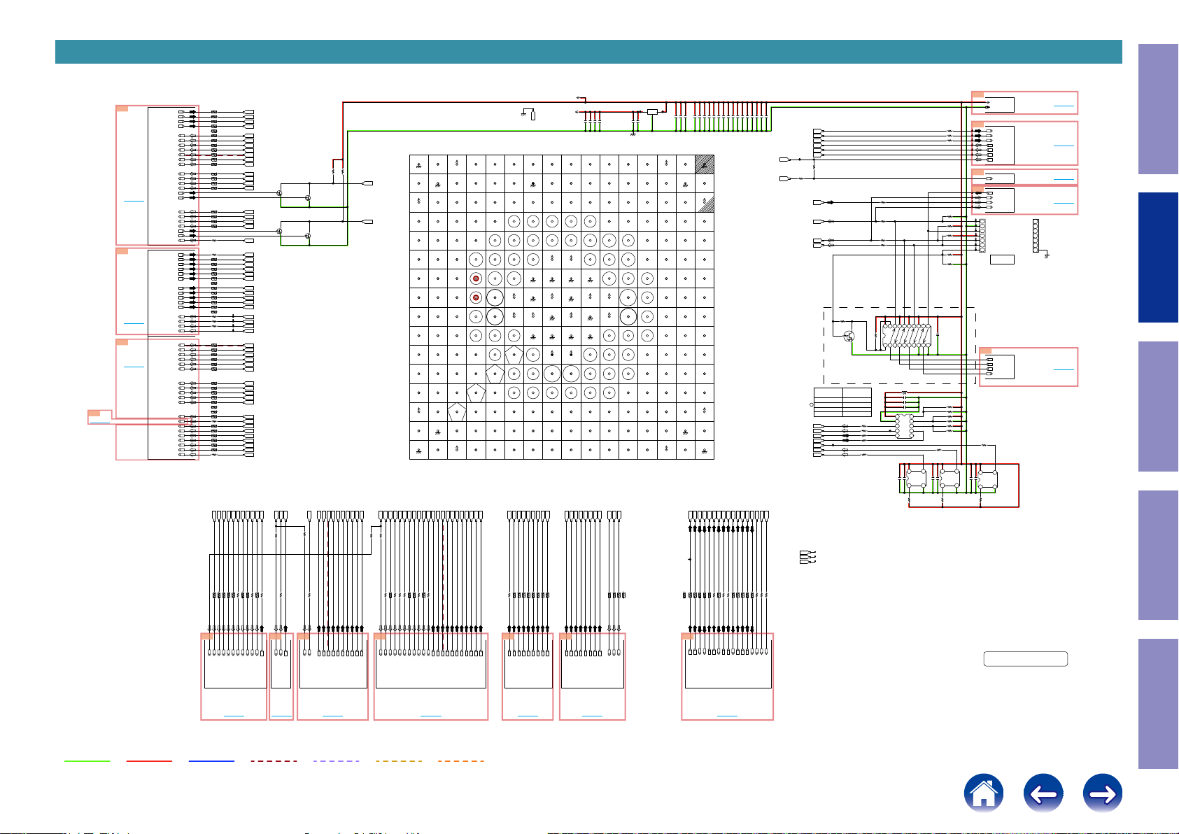
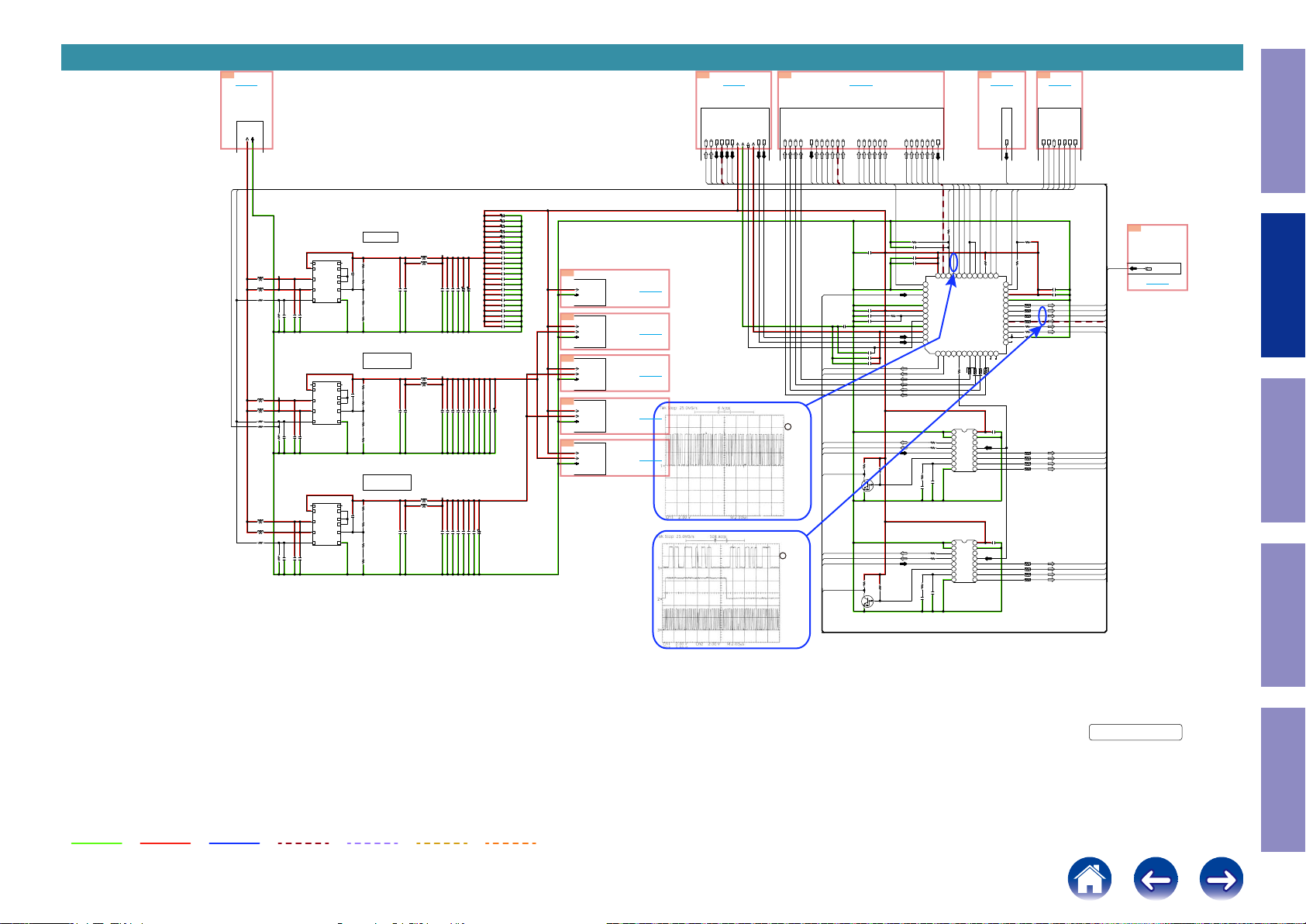
Page 11
SCH02_MAIN CPU
All Ref.No. has been described in the parts list are four digits.
But there are less than four digits of printed Ref.No. on the PCB, and they have become four digits after the header by adding "0" in the parts list.
A9
TO 9AB0TO 0BB1TO 1BB2TO 2BB3TO 3B
DSP_MISO
DSPI_CLK
DSP_MOSI
DSP4_FLAG0
DSP4_CS
DSP_RST
DSP4_WRITE
TO DSP3 TO DSP1TO DSP2TO DSP4
DSP_MISO
DSPI_CLK
DSP3_FLAG0
DSP3_CS
DSP_MOSI
DSP3_WRITE
DSP_RST
DSPI_CLK
DSP_MOSI
DSP_MISO
DSP2_CS
DSP2_FLAG0
DSP2_FLAG3
DSP_RST
DSP2_WRITE
TO 8U-310223(9/19) TO 8U-310223(8/19) TO 8U-310223(7/19) TO 8U-310223(6/19) TO 8U-310223(3/19)
DSPI_CLK
DSP_MISO
DSP_MOSI
DSP1_FLAG0
DSP1_CS
DSP_RST
AUDIO PLD
TO 8U-310223(4/19)
DSP1_WRITE
Z2PLDAERR
MAINPLDERR
Z3PLDAERR
APLD_DATA
APLD_CS1
APLD_CLK
.VOLMUTE
B4
TO 4B
DA POWER
TO 8U-310223(5/19)
MAINDIR_CE
MAINDIR_CLK
MAINDIR_DIN
MAINDIR_DOUT
DA_POWER2
DA_POWER1
OPEN
R6319
B5
TO EXPANDER
MAINDIR_RST
MIC_HP_DET
AEXP_CLK
DC_ASO_PROT
TO 5B
AEXP_STB
AEXP_OE
AEXP_DA_1IN
DGND
SWM5V
SWM3.3V
M3.3V
USB_SEL
8A
TO DIGITAL CONNECT
THERMALINE
FANDET_ON
FANDET_HIGH
THERMALINF
TRDET
232I_MO
232O_MI
MAINADC_RST
DAC_RST1
DAC_CDATA
DAC_CCS1
AMPSIGDET
AVSCL
TU_SCL
CURRENTDET
TU_SEN
TU_SDA
AVSDA
AC_RL1
DAC_CCLK
TU_INT
ZONEDATA
ZONESTB
ZONECLK
SEL_CLK
VOL_CLK
TO A8
TO 8U-310223(1/19)
DV5V
M3.3V
SWM3.3V
DV3.3V
SWM5V
4.7K
4.7K
10K
470K
OPEN
10K
OPEN
OPEN
DGND
NET_FACT_RST
MAINPW
RCOUT
RC_IN
FLASHERIN
ISELB
KEY2
VSELA
KEY1
POWERKEY
ISELA
KEY3
DOORDET
SEL_DATA
KILLIR
VOL_DATA
GREEN_LED
RED_LED
VSELB
MAIN_RST
FL_CTRL
FL_RST
FL_CLK
FL_DATA
FL_CE1
FL_CE2
REMOTE_POWER
CPU_POWER
R6298
R6296
R6283
R6285
R6511
R6284
R6288
R6286
MAIN_BDOWN
Caution in
servicing
B6
TO 6B
B7
TO 7B
B8
TO 8B
B9
TO 9B
C0
TO 0C
C1
TO 1C
C2
TO 2C
AVSDA
AVSCL
ARC_INT
ARC_RST
TO eARC
TO 8U-310223(18/19)
DV_POWER1
DV_POWER2
CEC_POWER1
CEC_POWER2
TO 8U-310223(10/19)
TO
HDMI SUPPLY
AVSCL
AVSDA
DE_RST
TO
DECODER
TO 8U-310223(11/19)
H5VDET
SW1_HINT
SW1_RST
TO
HDMI SW1
TO 8U-310223(13/19)
SW2_HINT
SW2_RST
TO 8U-310223(12/19)
TO
HDMI SW2
IP_SPISCK
IP_MOTXI
IP_MITXO.
IP_SPICS
IP_RST
TO
IP/OSD
GUI_WRITE
TO 8U-310223(14/19)TO 8U-310223(17/19)
TX_HINT
TX_HAINT
TX_RST
TO
HDMI TX
CEC_OUT
CEC_IN
M3.3V
DV3.3V
DV5V
HSCL
HSDA
HSCL
HSDA
HSCL
HSDA
R6313
R6314
R6219
R6300
R6217
R6218
AVSDA
AVSCL
ARC_INT
ARC_RST
DV_POWER1
DV_POWER2
CEC_POWER1
CEC_POWER2
AVSCL
AVSDA
DE_RST
H5VDET
SW1_HINT
HSCL
HSDA
SW1_RST
SW2_HINT
HSCL
HSDA
SW2_RST
IP_SPISCK
IP_MOTXI
IP_MITXO.
IP_SPICS
IP_RST
GUI_WRITE
HSCL
HSDA
TX_HINT
TX_HAINT
TX_RST
CEC_OUT
CEC_IN
E3
(USA)
(EUROPE)
OPEN
OPEN
OPEN
OPEN
O
R6295
R6202
R6203
R6204
R6205
E2
OPEN
OPEN
OPEN
OPENOPEN
O
OPEN
4.7K
4.7K
4.7K
4.7K
4.7K
E1C
(CHINA) (JAPAN)
OPEN
OPEN
OPEN
OPEN
OPEN
OPEN
AIOS4_STBY_STATUS
GUI_WRITE
NET3.3V_POWER
D5V_POWER(X6400:NC)
CEC_POWER1
DV_POWER1
DV_POWER2
MAINDIR_DIN
MAINDIR_CE
MAINDIR_DOUT
MAINDIR_CLK
MAINDIR_RST
TX_HAINT
DSP4_CS
DE_RST
TX_HINT
TX_RST
SW2_HINT
SW2_RST
SW1_HINT
SW1_RST
ARC_RST
TRDET
DA_POWER1
THERMALINE
THERMALINF
UNIT_TEMP
ARC_INT
CURRENTDET
AMPSIGDET
KEY3
KEY2
KEY1
SEL_CLK
DSP2_FLAG3
JP
OPEN
OPEN
O
OPEN
OPEN
OPEN
R9264
R9265
C9634
1K
R62071KR62081KR6209
123456
OPEN
R6206
123456
OPEN
R6210
OPEN
R6313
OPEN
R6314
DSPI_CLK
DSP_MISO
0
OPEN
OPEN
78
78
DSP_RST
DSP4_WRITE
DSP_MOSI
DSP4_FLAG0
DSP4_CS
R6299
R6257
R6253
R6211
C6201
R6212
R6213
R6214
R6215
C6202
C6203
R6216
C6204
C6205
123456
78
10Kx4
R6282
OPEN
OPEN
R6219
R6217
OPEN
R63000R6218
123456
78
10Kx4
R6287
DSPI_CLK
DSP_MOSI
DSP_MISO
OPEN
33
10K
33
0.1
33
33
33
33
0.1
0.1
33
0.1
0.1
DSP3_FLAG0
DSP3_CS
DSP_RST
DSP3_WRITE
133
134
135
136
P64
137
P63
138
P62
139
P61
140
VSS
141
P60
142
VCC
143
PD7/IRQ7/AN107
144
PG1
145
PD6/IRQ6/AN106
146
PG0
147
PD5/IRQ5/AN113
148
PD4/IRQ4/AN112
149
P97
150
PD3/IRQ3/AN111
151
VSS
152
P96
153
VCC
154
PD2/IRQ2/AN110
155
P95
156
PD1/IRQ1/AN109
157
P94
158
PD0/IRQ0/AN108
159
P93/AN117
160
P92/RXD7/AN116
161
P91/AN115
162
VSS
163
P90/TXD7/AN114
164
VCC
165
P47/IRQ15-DS/AN007
166
P46/IRQ14-DS/AN006
167
P45/IRQ13-DS/AN005
168
P44/IRQ12-DS/AN004
169
P43/IRQ11-DS/AN003
170
P42/IRQ10-DS/AN002
171
P41/IRQ9-DS/AN001
172
VREFL0
173
P40
174
VREFH0
175
AVCC0
176
P07/IRQ15
DSP_MOSI
DSPI_CLK
DSP_MISO
MAINPW
CPU_POWER
AIOS4_WAKEUP
33
R6255
130
131
132
PE4/AN102
PE3/AN101
PE5/IRQ5/AN103
AVSS0
AVCC14P03/IRQ115AVSS1
1
2
3
0.1
C6206
POWERKEY
DSP_RST
DSP2_FLAG3
DSP2_FLAG0
DSP2_CS
MIC_HP_DET
MAINADC_RST
0.1
C6207
126
127
128
129
VCC
P70
VSS
133:
134:
135:
P01/RXD6/IRQ9/AN1198P00/TXD6/IRQ8/AN1189PF5/IRQ410EMLE11PJ512VSS13PJ314VCL15VBATT
6
7
232O_MI
FANDET_ON/HIGH
RED_LED
PE6/IRQ6/AN104
-
DSP2_WRITE
DSP1_CS
DSP_MOSI
DSP_MISO
DSPI_CLK
DSP1_FLAG0
FL_CE1
FL_CLK
FL_CE2
FL_RST
H5VDET
FL_CTRL
FL_DATA
DC_ASO_PROT
33
33
R62241KR6225
R622233R6223
118
119
120
121
122
123
124
125
PA0
P66
P65
P67/IRQ15
TRSYNC/PG4
TRDATA1/PG3
TRDATA0/PG2
PE7/IRQ7/AN105
PE2/RXD12/IRQ7-DS/AN100
PE1/TXD12
PE0/SCK12
P05/IRQ13
2:
6:
P02/SCK6/IRQ10/AN120
0.1
0.1
33
C6209
C6208
R622133R6220
232I_MO
VSELA
GREEN_LED
VSELB
DSP_RST
DSP1_WRITE
ZONESTB
33
R6227
116
117
VSS
TRST#/PF418MD/FINED19XCIN20XCOUT21RES#22XTAL/P3723VSS24EXTAL/P3625VCC26UPSEL/P35(IN)/NMI
16NC17
4.7K
R6226
MAINPLDERR
Z2PLDAERR
Z3PLDAERR
USB_EN
ZONECLK
ZONEDATA
REMOTE_POWER
0.1
33
C6210
R622833R623033R623333R623133R6236
111
112
113
114
115
VCC
PA2/RXD5
TRCLK/PG5
TRDATA3/PG7
TRDATA2/PG6
PA1/SCK5/IRQ11
R6235
OPEN
680
4.7K
0.1
X6201
12MHz
R6234
C6211
R6229
1 3
10P
C6212
100
R6232
MAIN_RST
.VOLMUTE
APLD_DATA
APLD_CS1
APLD_CLK
ISELA
ISELB
VOL_CLK
.VOLMUTE
Z3PLDAERR
THERMALINF
OPEN
R9266
33
0.1
C6216
R9230
103
104
105
106
107
108
109
110
VCC
VSS
PA7
PA6
PA5
PA3/RXD5/SSCL5
PB0/RXD4/RXD6/IRQ12
PA4/TXD5/SSDA5/IRQ5-DS
U6201
R5F564MJCDFC
P34/SCK6/SCK0/IRQ428P33/TIOCD0/RXD6/RXD0/IRQ3-DS29P32/TIOCC0/TXD6/TXD0/IRQ2-DS30TMS/PF331TDI/PF2/RXD132P31/IRQ1-DS33P30/RXD134TCK/FINEC/PF1/SCK1
27
0.1
C6214
10P
C6213
0.1
C6215
FLASHERIN
RC_IN
MAIN_BDOWN
DOORDET
DAC_RST1
DAC_CCS1
APLD_CS1
Z2PLDAERR
APLD/DAC_CLK
APLD/DAC_DATA
33
R6261
97
98
99
101
102
100
P72
P71
PB2
PB3/SCK4/SCK6
89:
PC1/SCK5/IRQ12
PB1/TXD4/TXD6/IRQ4-DS
TD0/TXD1/PF036P27/SCK137P26/TXD138P25/RXD339VCC40P24/SCK341VSS
35
33
33
R623733R6241
R623833R624433R6243
TU_SEN
TU_SDA
TU_INT
AC_RL1
33
R6291
PB4
TU_SCL
DSP_RST
DA_POWER1
HSDA
HSCL
DSP3_CS
33
R624533R6247
94
PB7/TXD995PB6/RXD996PB5/SCK9
PC6/RXD8/IRQ13
UB/PC7/TXD8/IRQ14
P11/SCK2/IRQ1
P12/RXD2/IRQ2
P23/TXD343P22/SCK044P21/RXD0/IRQ9
P13/TXD2/IRQ3
42:
43:
44:
P15/RXD1/SCK3/IRQ5
P16/TXD1/RXD3/IRQ6
P87/TXD10/TIOCA2
P17/SCK1/TXD3/IRQ7
P20/TXD0/IRQ8
0.1
33
33
R624633R6250
R6315
C6217
VOL_DATA
KILLIR
MAINDIR_RST
MAINDIR_CE
MAINDIR_CLK
MAINDIR_DIN
MAINDIR_DOUT
DSP2_CS
MAINPLDERR
0.1
33
C6218
R624933R6248
89
90
91
92
VCC
VSS93P73
P74
P75/SCK11
PC0/IRQ14
PC2/RXD5
P76/RXD11
P77/TXD11
PC3/TXD5
PC4/SCK5
P80/SCK10
P81/RXD10
P82/TXD10
PC5/SCK8
VCC
P83/SCK10
VSS
P50/TXD2
P51/SCK2
P52/RXD2
P53
P10/IRQ0
VCC_USBA
VSS1_USBA
USBA_DP
USBA_DM
VSS2_USBA
PVSS_USBA
AVSS_USBA
USBA_PREF
AVCC_USBA
VSS_USB
USB0_DP
USB0_DM
VCC_USB
P14/IRQ4
P86/RXD10
42
33
R6251
-
E_RxD_MIEO
E_CTS_MIEO
E_RTS_MOEI
DC_ASO_PROT
MIC_HP_DET
AEXP_STB
AEXP_CLK
AEXP_OE
AEXP_DA_1IN
USB_SEL
AC_RL1
THERMALINE
THERMALINF
FANDET_ON
FANDET_HIGH
TRDET
232O_MI
232I_MO
MAINADC_RST
DAC_CDATA
DAC_CCLK
DAC_CCS1
DAC_RST1
CURRENTDET
TU_INT
ZONEDATA
ZONECLK
ZONESTB
SEL_CLK
VOL_CLK
DOORDET
SEL_DATA
VOL_DATA
KILLIR
TU_SDA
AVSCL
AVSDA
AMPSIGDET
TU_SCL
TU_SEN
KEY1
RCOUT
FLASHERIN
POWERKEY
RC_IN
RED_LED
GREEN_LED
FL_CE1
KEY3
VSELA
ISELB
VSELB
ISELA
MAIN_BDOWN
MAIN_RST
FL_CLK
FL_RST
FL_DATA
FL_CTRL
REMOTE_POWER
CPU_POWER
FL_CE2
KEY2
NET_FACT_RST
MAINPW
Electrical Mechanical Repair Information Updating
APLD/DAC_CLK
33
APLD_CLK
R6239
33
DAC_CCLK
R6240
APLD/DAC_DATA
OPEN
OPEN
OPEN
C6223
U6202
OPEN
R6269
R6267
R6263
OPEN
R6264
OPEN
88
87
0
R6201
86
85
84
83
82
81
80
79
78
77
76
75
74
73
72
71
70
69
68
67
66
65
64
63
62
61
60
59
58
57
56
55
54
53
52
51
50
49
48
47
46
45
4.7K
OPEN
4.7K
4.7K
4.7K
R6266
R6265
R6260
R6254
R6252
4.7K
4.7K
4.7K
R6256
R6258
R6262
4.7K
R6268
8
7
6
5
R6290
R6289
R6270
R6271
C6219
R6272
R6273
R6274
R6275
C6220
C6221
C6222
R6276
R6277
R6278
R6279
R6280
R6281
VCC
WP
SCL
SDA
A0
A1
A2
VSS
33
33
33
33
0.1
33
33
0
33
0.1
0.1
0.1
33
33
33
33
33
33
N6201
11P-FFC
1
2
3
4
5
6
7
8
9
10
11
1
2
3
4
RESET
VCC
TDO
TDI
GND
UB
MD
EMLE
TRST
TCK
TMS
DSP1_CS
CEC_POWER2
DSP_RST
DSP4_FLAG0
DSP3_FLAG0
DSP2_FLAG0
DSP1_FLAG0
DSPI_CLK
DSP_MISO
DSP_MOSI
AVSCL
AVSDA
IP_RST
IP_MOTXI
IP_SPISCK
IP_MITXO.
-
IP_SPICS
CEC_IN
CEC_OUT
AEXP_DA_1IN
AEXP_CLK
AEXP_OE
AEXP_STB
SEL_DATA
NET5V_POWER
RCOUT
NET_FACT_RST
E_TxD_MOEI
R6242
R6259
33
APLD_DATA
33
DAC_CDATA
UNIT_TEMP
C9633
OPEN
R9259
R9258
OPEN
OPEN
R9261
R9260
OPEN
OPEN
OPEN
R9262
OPEN
R9263
NET_FACT_RST
E_CTS_MIEO
E_RTS_MOEI
E_RxD_MIEO
E_TxD_MOEI
NET5V_POWER
NET3.3V_POWER
USB_SEL
USB_EN
AIOS4_WAKEUP
AIOS4_STBY_STATUS
DSP4_WRITE
DSP3_WRITE
DSP2_WRITE
DSP1_WRITE
R6533
10K
FANDET_ON
FANDET_HIGH
FANDET_ON/HIGH
R6514
3.3K
R6515
3.9K
C3
NET_FACT_RST
E_CTS_MIEO
E_RTS_MOEI
E_RxD_MIEO
E_TxD_MOEI
NET5V_POWER
NET3.3V_POWER
USB_SEL
USB_EN
AIOS4_WAKEUP
AIOS4_STBY_STATUS
DSP4_WRITE
DSP3_WRITE
DSP2_WRITE
DSP1_WRITE
M3.3V
MAIN CPU
8U-310223(2/19)
DIGITAL_UNIT
Condential
TO
NETWORK MODULE
CONNECT
TO 8U-310223(19/19)
TO 3C
GND LINE
POWER+ LINE
POWER- LINE
AUDIO SIGNAL
TMDS SIGNAL
ANALOG VIDEO
DIGITAL VIDEO
11
Page 12
SCH03_EXPANDER
All Ref.No. has been described in the parts list are four digits.
But there are less than four digits of printed Ref.No. on the PCB, and they have become four digits after the header by adding "0" in the parts list.
Caution in
servicing
5B
TO CPU
TO 8U-310223(2/19)
USB_SEL
SWM3.3V
AEXP_DA_1IN
AEXP_OE
AEXP_STB
AEXP_CLK
MIC_HP_DET
DC_ASO_PROT
TO B5
M3.3V
DGND
SWM5V
USB_SEL
AEXP_DA_1IN
AEXP_OE
AEXP_STB
AEXP_CLK
MIC_HP_DET
DC_ASO_PROT
AEXP_DA_1IN
AEXP_OE
AEXP_STB
AEXP_CLK
R6513
R6512
0.1
C6500
4.7K
U6500
CD74HC4094PWR
R6504
C6501
OPEN
R6505
10K
MIC_HP_DET
R6506
3.3K
10K
4.7K
C4
TO 4CC5TO 5CC6TO 6C
TO
HDMI
SW2
TO 8U-310223(12/19) TO 8U-310223(13/19) TO 8U-310223(17/19) TO 8U-310223(16/19)
HPD4
HPD1
HPD2
HPD3
HPD2
HPD8
HPD7
HPD6
HPD5
10
11Q812Q713Q614Q515OE16
Q'S
VDD
STB2DATA3CLK4Q15Q26Q37Q48VSS
1
HPD3
HPD4
HPD2
HPD1
R6509
3.9K
Q6504
KTC3875S
R6517
OPEN
HPD1
9
QS
HPD4
HPD3
0.1
VDD
STB2DATA3CLK4Q15Q26Q37Q48VSS
CD74HC4094PWR
1
C6504
U6501
Q6505
KRC102S
(10K-10K)
HINSELA
HINSELB
HINSELC
HINSELC
TO
HDMI
SW1
HINSELB
HINSELC
HINSELB
HINSELA
10
11Q812Q713Q614Q515OE16
Q'S
MIC_DET
HPD7
HINSELA
HPD6
HPD7
9
QS
H/P_DET
HPD6
HPD5
0.1
C6506
TO
HDMI
Tx
HPD5
VDD
STB2DATA3CLK4Q15Q26Q37Q48VSS
CD74HC4094PWR
1
U6502
LEGO_FAN_POWER
HPD8
HPD8
DAC_RST2
TTL_SELA
TTL_SELB
DAC_CCS2
11Q812Q713Q614Q515OE16
SD/HD
DC_ASO_PROT
C7
9
10
QS
Q'S
Q6501
R6507
OPEN
TO 7C
TO
VIDEO
PLD
VPLD_TRANS2
VPLD_TRANS0
VPLD_TRANS1
TTL_SELB
TTL_SELB
VPLD_TRANS2
VPLD_TRANS0
VPLD_TRANS1
0.1
CD74HC4094PWR
C6510
U6503
R6532
10K
R6535
3.3K
OPEN
C6502
OPEN
SD/HD
TTL_SELA
TTL_SELA
SD/HD
TU_RST
MDAX_LED
ILLUMI_LED
VDD
STB2DATA3CLK4Q15Q26Q37Q48VSS
1
VPLD_TRANS2
VPLD_TRANS0
VPLD_TRANS1
DCDET
ASODET
R6539
3.9K
-
R6508
OPEN
Q6502
OPEN
-
11Q812Q713Q614Q515OE16
10
DIRECT_LED
R6540
Q'S
8.2K
9
QS
0.1
CD74HC4094PWR
C6513
U6504
LEGODET
4.7u
C6505
OPEN
C6503
R6510
TRIGGER1
TRIGGER2
LEGO_FAN_POWER
9
10
11Q812Q713Q614Q515OE16
QS
Q'S
VDD
STB2DATA3CLK4Q15Q26Q37Q48VSS
1
LEGODET
22K
R6516
Q6503
KTC3875S
Z6501
PRF18BF471QB5RB
N6501
OPEN
1
+5V
2
TO LEGO FAN
3
DGND
7A
TO DIGITAL CONNECT
TO 8U-310223(1/19)
TRIGGER1
DAC_CCS2
TRIGGER2
DAC_RST2
TU_RST
DCDET
4.7K
TRIGGER2
TRIGGER1
DCDET
TU_RST
DAC_CCS2
DAC_RST2
TO A7
ASODET
ASODET
MDAX_LED
ILLUMI_LED
ILLUMI_LED
MDAX_LED
DIRECT_LED
DIRECT_LED
Electrical Mechanical Repair Information Updating
AEXP_STB
AEXP_CLK
AEXP_OE
AEXP_DA_6OUT
MIC_DET
H/P_DET
H/P_DET
MIC_DET
AEXP_DA_6OUT
AEXP_OE
AEXP_STB
AEXP_CLK
EXPANDER
8U-310223(3/19)
DIGITAL_UNIT
Condential
GND LINE
POWER+ LINE
POWER- LINE
AUDIO SIGNAL
TMDS SIGNAL
ANALOG VIDEO
DIGITAL VIDEO
12
Page 13
SCH04_AUDIO PLD
0A
TO A0
C8
4A
C9
TO 8C
TO A4
TO 9C
TO DIR
TO CONNECT
TO CONNECT
Z2NETADC_DATA
Z2NETADC_fs
Z2NETADC_64fs
Z2NETADC_256fs
MAINDIR_XIN
MAINDIR256fs
MAINDIR64fs
MAINDIRfs
MAINDIRDATA
MAINDIRAUDIO
MAINDIRERR
Z2DIR256fs
Z2DIR64fs
Z2DIRfs
Z2DIRDATA
TO 8U-310223(5/19)
Z2DIRAUDIO
Z2DIRERR
Z3DIR256fs
Z3DIR64fs
Z3DIRfs
Z3DIRDATA
Z3DIRAUDIO
Z3DIRERR
HDMI_SPDIF
DLHD
Z2DAC_256fs
Z2DAC_64fs
Z2DAC_fs
Z2DAC_DATA
Z2DAC_MUTE
Z3DAC_256fs
Z3DAC_64fs
Z3DAC_fs
Z3DAC_DATA
Z3DAC_MUTE
TO 8U-310223(1/19)
MAINADC_256fs
MAINADC_64fs
MAINADC_fs
MAINADC_DATA
DAC1_F/FR
DAC1_C/C
DAC1_S/SW1
DAC1_SW2/SL
DAC1_-/SR
DAC1_-/SW2
DAC2_F/FR
DAC2_C/C
DAC2_S/SW1
DAC2_SW2/SL
DAC2_-/SR
TO 8U-310223(1/19)
DAC1_BCK//CK
DAC1_MCLK
DAC1_LRCK/FL
DAC2_LRCK/FL
NETDAC_MCLK
NETDAC_BCK
NETDAC_LRCK
NETDAC_DATA
NETDAC_MUTE
INPUT
-
INPUT
-
INPUT
-
INPUT
-
OUTPUT
OUTPUT
OUTPUT
OUTPUT
OUTPUT
OUTPUT
OUTPUT
OUTPUT
OUTPUT
OUTPUT
OUTPUT
INPUT
-
INPUT
-
OUTPUT
OUTPUT
OUTPUT
OUTPUT
INPUT
-
INPUT
-
OUTPUT
INPUT
-
INPUT
-
INPUT
-
INPUT
-
INPUT
-
INPUT
-
INPUT
-
INPUT
-
INPUT
-
INPUT
-
INPUT
-
OUTPUT
OUTPUT
OUTPUT
OUTPUT
OUTPUT
OUTPUT
OUTPUT
OUTPUT
OUTPUT
OUTPUT
OUTPUT
OUTPUT
OUTPUT
OUTPUT
OUTPUT
OUTPUT
OUTPUT
OUTPUT
OUTPUT
OUTPUT
OUTPUT
OUTPUT
OUTPUT
OUTPUT
R1268
R1268
R1268
R1268
R9235
R1294
R1249
R1248
R1240
R1284
R9233
R9233
R9233
R9233
R9234
7
5
3
1
3
1
7
5
3
1
7
5
1
3
5
7
1
3
5
7
5
3
7
1
5
7
1
7
3
5
1
3
7
5
3
1
7
5
3
1
7
5
3
1
3
1
7
5
2
4
6
8
100x4
8
100x4
6
100x4
4
100x4
2
100x4R1252
4
100x4R1252
2
100x4R1278
8
100x4R1278
6
100x4R1278
4
100x4R1278
2
100x4R1252
8
100x4R1252
6
100x4R1253
2
100x4R1253
4
100x4R1253
6
100x4R1253
8
100x4R1277
2
100x4R1277
4
100x4R1277
6
100x4R1277
8
33
100
100x4R1206
6
100x4R1206
4
100x4R1280
8
100x4R1206
2
100x4R1280
6
100x4R1206
8
100x4R1280
2
100x4R1281
8
100x4R1281
4
100x4R1281
6
100x4R1281
2
100x4R1280
4
33
33
33
100x4R1212
8
100x4R1212
6
100x4R1212
4
100x4R1212
2
100x4R1203
8
100x4R1203
6
100x4R1203
4
100x4R1203
2
100x4R1202
8
100x4R1202
6
100x4R1202
4
100x4R1287
2
100x4R1287
4
100x4R1202
2
33
100x4R1287
8
100x4R1287
6
33x4
1
33x4
3
33x4
5
33x4
7
33
.DSP1IN256fs
B6
.DSP1IN64fs
B5
.DSP1INSWC/C
.DSP1INS/SL
.DSP1INRSV/FR
.DSP1INfs
A6
C5
C6
A7
M14
.Z2NETADC_DATA
M16
.Z2NETADC_fs
M15
.Z2NETADC_64fs
L5
.Z2NETADC_256fs
K15
.MAINDIR_XIN
P15
.MAINDIR256fs
N15
.MAINDIR64fs
N16
.MAINDIRfs
M13
.MAINDIRDATA
L16
.MAINDIRAUDIO
K14
.MAINDIRERR
H15
.Z2DIR256fs
G14
.Z2DIR64fs
F13
.Z2DIRfs
F14
.Z2DIRDATA
E14
.Z3DIR256fs
D14
.Z3DIR64fs
D13
.Z3DIRfs
D12
.Z3DIRDATA
N14
.HDMI_SPDIF
.DLHD
M2
.Z2DAC_256fs
B3
.Z2DAC_64fs
D4
.Z2DAC_fs
C3
.Z2DAC_DATA
A2
.Z2DAC_MUTE
B1
.Z3DAC_256fs
C2
.Z3DAC_64fs
D2
.Z3DAC_fs
D3
.Z3DAC_DATA
D1
.Z3DAC_MUTE
E4
.MAINADC_256fs
M8
.MAINADC_64fs
M9
.MAINADC_fs
B4
MAINADC_DATA
C4
.DAC1_F/FR
G1
.DAC1_C/C
G2
.DAC1_S/SW1
G3
.DAC1_SW2/SL
H1
.DAC1/-/SR
H2
.DAC1/-/SW2
H3
.DAC2_F/FR
J1
.DAC2_C/C
J2
.DAC2_S/SW1
J3
.DAC2_SW2/SL
K1
.DAC2/-/SR
K2
.DAC1_BCK//CK
K3
.DAC1_MCLK
E1
.DAC1_LRCK/FL
L1
.DAC2_LRCK/FL
L2
.NETDAC_MCLK
E2
.NETDAC_BCK
E3
.NETDAC_LRCK
F1
.NETDAC_DATA
F2
.NETDAC_MUTE
F3
.DSP1INLR
.DSP1INF/FL
.DSP1INRSV/SW
.DSP1INSB/SR
A8
A5
A4
C7
10k/10k
10k/10k
.DSP1_FLAG3B8DSP_2_3_CLKOUT
22
R1243
D11
Q8011
KRC402E-RTK
Q8013
KRC402E-RTK
.DSP2IN256fs
DSP2_FLAG3
D15
D16
All Ref.No. has been described in the parts list are four digits.
But there are less than four digits of printed Ref.No. on the PCB, and they have become four digits after the header by adding "0" in the parts list.
Caution in
servicing
33
R1216
33
R1214
33
R1215
R1228
1K
R1229
10K
R1230
10K
R1207
1K
R1303
OPEN
0.1
TC74VHC244FT
C1202
U1207
10K
R1231
OPEN
R1232
OPEN
R1233
R1234
10K
OPEN
R1235
10K
R1236
33
U1206
25.0M
3
4
0.1
OUT
VDD
GND
ST
TXC_8W
1
2
C1232
R1273
10K
D0
3B
D1
D2
R1222
1000P
0.1
C1223
C1224
OUTPUT
OUTPUT
OUTPUT
OUTPUT
OUTPUT
OUTPUT
OUTPUT
1
2
3
4
5
6
7
N1201
7P-FFC
D3
OUTPUT
4
ST
1
R1213
10K
DA3.3V
DGND
MAINPLDERR
Z2PLDAERR
Z3PLDAERR
INPUT
APLD_CLK
INPUT
APLD_DATA
INPUT
APLD_CS1
INPUT
.VOLMUTE
VOLMUTE
INPUT
SUB_TDO
SUB_TMS
.TDO1_TDI2
SUB_TCK
TCK
GND
TDO
VCC
TMS
TDI
GND
T.P
INPUT
PLD_TCK_WR
INPUT
PLD_TMS_WR
INPUT
PLD_TDI_WR
PLD_TDO_WR
33
OUT
VDD
FCXO-05
SUB_TDI
TDO1_TDI2
SUB_TDO
3
GND
2
U1201
22.5792M
↓
↓
TO DIR/
DA POWER
TO 8U-310223(5/19)
TO CPU
TO 8U-310223(2/19)
TO CONNECT
TO 8U-310223(1/19)
TO
VIDEO
PLD
TO 8U-310223(16/19)
1
2
3
AUDIO PLD
USB Blaster
4
5
VIDEO PLD
6
7
TO
NET
MODULE
CONNECT
TO 8U-310223(19/19)
TO 0D
TO B3
TO 1D
TO 2D
Electrical Mechanical Repair Information Updating
TO 3D
DA3.3V
DA1.8V
B7
DGND
DGND
1A2 3 4 5 6 7 8 9
A1 A2 A3 A4 A5 A6 A7 A8 A9
10K
10K
R9231
R9232
L14
N13
Z2DIRERR
Z3DIRERR
Q8012
KRC402E-RTK
10k/10k
Q8014
KRC402E-RTK
10k/10k
5M570ZF256C5N
DSP3OUT64fs
DSP3OUTfs
DSP3OUTSB
DSP1_4_CLKOUT
DSP3_FLAG3
DSP3OUTFW
DSP3OUTF
DSP3OUTCSW1
.DSP3IN256fs
DSP3OUTS
DSP3OUTFH
DSP3OUTRSV
22
R1261
H16
J16
J14
E16
F15
J15
D5
F16
K16
G16
E15
G15
22
R127622R1282
.Z2DAC_DATA
DA3.3V
DGND
B1 B2 B3 B4 B5 B6 B7 B8 B9
B
.Z2DAC_MUTE
.Z2DAC_256fs
DGND
C1 C2 C3 C4 C5 C6 C7 C8 C9
C
.Z3DAC_256fs
.Z2DAC_fs
DA3.3V
D1 D2 D3 D4 D5 D6 D7 D8 D9
D
.Z3DAC_DATA
.Z3DAC_64fs
.Z3DAC_fs
E1 E2 E3 E4 E5 E6 E7 E8 E9
E
F
G
H
J
K
L
M
N
P
R
T
U9103
.DSP4IN64fs
.DSP4INfs
.DSP4IN256fs
.DSP4INF
C9
B13
A12
A11
.NETDAC_BCK
.NETDAC_MCLK
.DAC1_MCLK
F1 F2 F3 F4 F5 F6 F7 F8 F9
.NETDAC_MUTE.NETDAC_DATA.NETDAC_LRCK
G1 G2 G3 G4 G5 G6 G7 G8 G9
.DAC1_S/SW1
.DAC1_C/C
.DAC1_F/FR
H1 H2 H3 H4 H5 H6 H7 H8 H9
.DAC1/-/SW2
.DAC1/-/SR
.DAC1_SW2/SL
J1 J2 J3 J4 J5 J6 J7 J8 J9
.DAC2_S/SW1
.DAC2_C/C
.DAC2_F/FR
K1 K2 K3 K4 K5 K6 K7 K8 K9
.DAC2/-/SR
.DAC2_SW2/SL
.DAC1_BCK//CK
L1 L2 L3 L4 L5 L6 L7 L8 L9
.TX64fs
.DAC2_LRCK/FL.DAC1_LRCK/FL
M1 M2 M3 M4 M5 M6 M7 M8 M9
RSV0
.DLHD
CSERR
N1 N2 N3 N4 N5 N6 N7 N8 N9
ARCSPDIF/DSD0
ARCI2S3/DSD4
ARC_MUTE.
DA3.3V
ARCI2S1/DSD2
.DSP4INS
.DSP4INCSW
B10
C10
K
K
P1 P2 P3 P4 P5 P6 P7 P8 P9
SUB_TCK
ARCI2S2/DSD3
R1 R2 R3 R4 R5 R6 R7 R8 R9
ARCfs/DSD5
DGND
T1 T2 T3 T4 T5 T6 T7 T8 T9
ARCI2S0/DSD1
DA3.3V
DGND
DSP4OUTCSW1
.DSP4INFH
.DSP4INFW
DSP4OUTS
DSP4OUTF
.DSP4INSB
.DSP4INRSV
DSP4OUTfs
DSP4OUT64fs
DSP4OUTSB
A9
B9
C8
C11
C14
B16
A10
B14
C13
B12
.DSP1INRSV/SW
MAINADC_DATA
.Z2DAC_64fs
.Z3DAC_MUTE
.TXI2S0
CSREFIN
M
M
SUB_TMS
ARC64fs/DSDSCK
ARC256fs/DSDMCK
RXSPDIF/DSD0
DSP4OUTFH
DSP4OUTSW2RSV
DSP4OUTFW
B11
A15
A13
.DSP1INF/FL
.DSP1IN64fs
.DSP1INS/SL
DSP1_4_CLKOUT
CKIN
CKIN
CSCKIN
CKIN
CKIN
CSCKOUT
O
O
TDO1_TDI2
.TXfs
RX256fs/DSDMCK
RX64fs/DSDSCK
RXI2S3/DSD4
DSP4_FLAG3
DSP4OUTRSV
C15
C12
.DSP1INSWC/C
.DSP1IN256fs
.DSP1INRSV/FR
DA3.3V
DA3.3V
I
I
SUB_TDI
RXI2S2/DSD3
.NET_I2S2_DOUT
RXI2S1/DSD2
.NET_I2S2_DIN
RXI2S0/DSD1
ARCSPDIF/DSD0
ARC64fs/DSDSCK
ARC256fs/DSDMCKN1ARC_MUTE.
P4
N2
R4
.DSP1INfs
DGND
.DSP1INSB/SR
DGND
DGND
DA1.8V
DGND
RXfs/DSD5
ARCI2S0/DSD1
ARCI2S1/DSD2
R1
T2
.DSP1_FLAG3.MAINADC_fs
.MAINADC_256fs
.NET_TDM_DOUT
.NET_TDM_DIN
.NET_I2S0_DOUT
ARCI2S3/DSD4
ARCI2S2/DSD3
N3
P2
.DSP1INLR
.DSP4INRSV
DA3.3V
DA1.8V
DA3.3V
ARCfs/DSD5
R3
0.1
0.1
0.1
0.1
C1234
C1235
C1230
C1233
10 11 12 13 14 15 16
A10 A11 A12 A13 A14 A15 A16
.DSP4INFH
.DSP4INF
.DSP4INSB
B10 B11 B12 B13 B14 B15 B16
DSP4OUTFH
.DSP4INFW
.DSP4INS
C10 C11 C12 C13 C14 C15 C16
.DSP4IN64fs
.DSP4INCSW
DSP4OUTCSW1
D10 D11 D12 D13 D14 D15 D16
DSP_2_3_CLKOUT
E10 E11 E12 E13 E14 E15 E16
F10 F11 F12 F13 F14 F15 F16
DA3.3V
G10 G11 G12 G13 G14 G15 G16
DGNDDGND
DGND
H10 H11 H12 H13 H14 H15 H16
DA1.8V
DA3.3V
DGND
J10 J11 J12 J13 J14 J15 J16
DA1.8V
DGND
DGND
.MAINADC_64fs
.NET_I2S_MCKOUT
.NET_SPDIFOUT
.NET_I2S0_DIN
DA3.3V
DGND
K10 K11 K12 K13 K14 K15 K16
DGND
DGND
L10 L11 L12 L13 L14 L15 L16
DA3.3V
M10 M11 M12 M13 M14 M15 M16
N10 N11 N12 N13 N14 N15 N16
P10 P11 P12 P13 P14 P15 P16
.NET_I2S0_LRCKOUT
.NET_TDM_FSIN
R10 R11 R12 R13 R14 R15 R16
.NET_I2S0_BCLKOUT
.NET_I2S2_LRCKIN
T10 T11 T12 T13 T14 T15 T16
.NET_I2S2_BCKIN
.NET_TDM_BCKIN
RXSPDIF/DSD0
RX64fs/DSDSCK
RXI2S2/DSD3
RXfs/DSD5
RX256fs/DSDMCK
RXI2S0/DSD1T6RXI2S3/DSD4
RXI2S1/DSD2
T4
R5
P6
P7
P5
T5
R6
.TX64fs
L3
N5
.DSP4IN256fs
DSP4OUTSB
DSP4OUTRSV
.Z3DIRDATA
APLD_DATA
NOT_USE1
NOT_USE2
NOT_USE3
.TXI2S0
.TXfs
L4
C1201
4.7u
1608
CKIN
CKIN
OSC25M
CKIN
CKIN
OSC24M
U1202
NJM2845DL1-18
OUT
C1203
1000P
DGND
DSP4OUTFW
.DSP4INfs
DSP4OUT64fs
.Z3DIRfs
.VOLMUTE
.Z2DIRfs
OSC22M
.MAINDIRDATA
Z3DIRERR
.PLDAERRMAIN
APLD_CLK
APLD_CS1
IN
DA3.3V
DSP4OUTfs
DSP4OUTS
.Z3DIR64fs
.Z3DIR256fs
.Z2DIRDATA
.Z2DIR64fs
DSP3OUTF
.MAINDIRERR
Z2DIRERR
.Z2NETADC_DATA
.HDMI_SPDIF
.Z2PLDAERR
DA3.3V
RSV3
RSV2
4.7u
0.1
1608
C1209
C1211
DSP4OUTSW2RSV
DSP4_FLAG3
.DSP2IN256fs
DSP3OUTFH
.DSP3IN256fs
DSP3OUTRSV
.Z2DIR256fs
DSP3OUTS
.MAINDIR_XIN
.Z2NETADC_256fs
.Z2NETADC_64fs
.MAINDIR64fs
.MAINDIR256fs
.Z3PLDAERR
1000P
C1213
DGND
DGND
0.1
0.1
C1205
C1204
DGND
DSP4OUTF
DA3.3V
DSP2_FLAG3
DSP3OUTCSW1
DSP3OUTSB
DSP3OUTFW
DSP3OUT64fs
DSP3OUTfs
DSP3_FLAG3
.MAINDIRAUDIO
.Z2NETADC_fs
.MAINDIRfs
DA3.3V
RSV1
DGND
.NET_I2S_MCKOUT
.NET_SPDIFOUT
P9
R9
R10
0.1
0.1
0.1
0.1
0.1
0.1
0.1
0.1
C1216
C1215
C1207
C1206
C1210
C1214
C1208
C1212
.NET_I2S0_DIN
.NET_I2S2_LRCKIN
.NET_I2S0_BCLKOUT
.NET_I2S2_DOUT
.NET_TDM_DOUTP8NOT_USE2
.NET_I2S2_DIN
.NET_I2S0_DOUTT8.NET_I2S0_LRCKOUT
.NET_I2S2_BCKIN
T9
R7
T7
R11
P11
T10
1000P
1000P
1000P
1000P
C1222
C1217
C1227
C1218
RSV3
.NET_TDM_FSIN
.NET_TDM_BCKIN
NOT_USE1
.NET_TDM_DIN
R8
P10
T11
P12
1000P
1000P
C1229
C1228
.VOLMUTE
R12
NOT_USE3
T12
.PLDAERRMAIN
P13
.Z2PLDAERR
R14
.Z3PLDAERR
T15
APLD_CLK
R13
APLD_DATA
N12
APLD_CS1
T13
RSV3
RSV1
RSV2
R9224
OPEN
TDO1_TDI2
SUB_TCK
SUB_TMS
SUB_TDI
CSCKOUT
CSCKIN
CSREFIN
OSC22M
OSC25M
OSC24M
.VOLMUTE
0
R9229
L1201
C1219
C1220
C1221
VD
1
2
3
4
5
U1203
CS2100-10-CZZR
0.1
1000P
C1225
C1226
11A121
4.7u
0.1
1000P
M0
10
M1
9
M2
8
XTI/REF_CLK
7
XTO
6
U1205
24.576M
4
VDD
ST
FCXO-05
1
R1227
10K
OUT
R1274
3
GND
2
SUB_TDO
11
2A1121Y4132A2141Y3152A3161Y2172A4181Y1192OE20VCC
GND
10
1000P
C1231
M5
P3
N4
L6
Q1201
KRC402E-RTK
10k/10k
J5
CSERR
M3
H5
M4
L13
H12
J12
H14
R16
P14
R1292
OPEN
-
-
SUB_TDI
R1217
R1218
R1219
R1220
R1221
R1223
100
R1224
100
R1225
100
4.7K
R1201
33
33
33
33
33
1OE21A132Y441A252Y361A372Y281A492Y1
1
GND
CLK_OUT
AUX_OUT
CLK_IN
R1211
100
TDO1_TDI2
E13
RSV0
M1
GND LINE
POWER+ LINE
100x4
100x4R1204
100x4
2
6
1
123
5
R1263
R1263
D4
OUTPUT
OUTPUT
OUTPUT
OUTPUT
DSP1IN64fs
DSP1_CLKIN
DSP1IN256fs
TO DSP1
TO 8U-310223(6/19)
TO 4DD5TO 5D
POWER- LINE
100x4
100x4
100
4
7856347
R1204
R1263
OUTPUT
OUTPUT
DSP1INfs
DSP1INF/FL
DSP1INSWC/C
R1200
OUTPUT
100
100x4
100x4
100x4
100
8
R1267
R1208
R1204
R1263
R1204
-
OUTPUT
OUTPUT
OUTPUT
OUTPUT
INPUT
DSP1INLR
DSP1INS/SL
DSP1_FLAG3
DSP1INSB/SR
DSP1INRSV/FR
DSP1INRSV/SW
TO 8U-310223(7/19)
AUDIO SIGNAL
100
R1271
OUTPUT
OUTPUT
DSP2_CLKIN
DSP2IN256fs
TO
DSP2
-
INPUT
DSP2_FLAG3
100
R1205
D6
OUTPUT
OUTPUT
INPUT
INPUT
DSP3OUTfs
DSP3_CLKIN
DSP3IN256fs
DSP3OUT64fs
TO DSP3
TO 8U-310223(8/19)
TO 6D
TMDS SIGNAL
---------
INPUT
INPUT
INPUT
DSP3OUTF
DSP3OUTS
DSP3OUTCSW1
INPUT
INPUT
INPUT
DSP3OUTFH
DSP3OUTSB
-
INPUT
INPUT
DSP3OUTFW
DSP3OUTRSV
DSP3_FLAG3
100x4
100x4
100x4
100
100
100
100
4
8
3
R1239
R1239
R1239
R1209
R1210
R1238
R1256
D7
OUTPUT
OUTPUT
OUTPUT
OUTPUT
OUTPUT
OUTPUT
OUTPUT
OUTPUT
DSP4INF
DSP4INS
DSP4INSB
DSP4INfs
DSP4INCSW
DSP4IN64fs
DSP4_CLKIN
DSP4IN256fs
ANALOG VIDEO
100x4
100
100
12567
R1239
R1254
R1255
---
OUTPUT
OUTPUT
OUTPUT
INPUT
INPUT
INPUT
INPUT
DSP4INFW
DSP4INFH
DSP4OUTF
DSP4INRSV
DSP4OUTfs
DSP4OUTCSW1
DSP4OUT64fs
TO DSP4
TO 8U-310223(9/19)
TO 7D
DIGITAL VIDEO
-----
INPUT
DSP4OUTS
INPUT
-
INPUT
INPUT
DSP4OUTFH
DSP4OUTFW
DSP4OUTSB
-
-
INPUT
INPUT
INPUT
DSP4OUTRSV
DSP4_FLAG3
DSP4OUTSW2RSV
100x4
100
100x4
100x4
100x4
2
6
7834341
1
R1251
R1242
R1242
R1242
R1226
-
-
D8
INPUT
INPUT
INPUT
INPUT
INPUT
ARC64fs
ARCI2S0
ARCI2S1
ARCSPDIF
ARC256fs
TO eARC
TO 8U-310223(18/19)
TO 8D
100x4
100x4
2
R1226
R1226
-------
INPUT
ARCI2S2
INPUT
ARCI2S3
100x4
100x4
78565
R1242
R1226
INPUT
ARCfs
INPUT
ARC_MUTE
RXSPDIF is common port with ARC
-
D9
INPUT
INPUT
INPUT
RXSPDIF/DSD0
RX64fs/DSDSCK
RX256fs/DSDMCK
TO HDMI TX
TO 8U-310223(17/19)
INPUT
INPUT
INPUT
INPUT
RXI2S3/DSD4
RXI2S1/DSD2
RXI2S0/DSD1
RXI2S2/DSD3
TO 9D
13
-------
INPUT
RXfs/DSD5
33x4
33x4
4
3
R1237
R1237
OUTPUT
OUTPUT
TX64fs
8
7
TXfs
33x4
33x4
6
5
R1237
R1237
OUTPUT
TXI2S0
0
0
100x4
0x4
0x4
0x4
100x4
0x4
2
1
4
3
R1260
4
3
R1244
R1244
100x4
R1245
R1245
8
R1244
R1241
567812567
R13080R1309
R1244
100x4
100x4
R1260
R1260
100x4
7834561
100x4
2
R1245
R1245
100
100x4
2
1
R1260
R1304
100
R1305
100
R1307
AUDIO PLD
E0
OUTPUT
OUTPUT
INPUT
INPUT
NET_SPDIFOUT
NET_I2S2_BCKIN
NET_I2S_MCKOUT
NET_I2S2_LRCKIN
TO NET
MODULE CONNECT
OUTPUT
OUTPUT
INPUT
INPUT
INPUT
INPUT
INPUT
NET_I2S2_DIN
NET_I2S0_DIN
NET_TDM_DOUT
NET_I2S0_DOUT
NET_I2S2_DOUT
NET_I2S0_BCLKOUT
NET_I2S0_LRCKOUT
TO 8U-310223(19/19)
TO 0E
OUTPUT
OUTPUT
OUTPUT
INPUT
INPUT
NET_TDM_DIN
AIOS4_GPIO_1
AIOS4_GPIO_0
NET_TDM_FSIN
NET_TDM_BCKIN
OUTPUT
AIOS4_GPIO_2
8U-310223(4/19)
DIGITAL_UNIT
Condential
Page 14
SCH05_DIR DA SUPPLY
1A
TO A1
TO CONNECT
TO 8U-310223(1/19)
D5V
DA_POWER2
DA_POWER1
R1911
R1912
R1906
R1932
DGND
L1901
BLM21PG221
L1902
OPEN
10
L1905
BLM21PG221
L1906
OPEN
10
OPEN
L1909
BLM21PG221
L1910
OPEN
10
0.1
47K
C1901
R1901
47K
R1913
0.1
47K
C1940
R1933
0.1
C1913
10/16
1u
C1903
C1902
1u
10/16
C1915
C1914
10/16
1u
C1942
C1941
U1901
XCL212B082DR
NC
1
NC
4
L2
11
10
L1
2
LX
9
PVIN
3
LX
7
5
AVIN
FB
GND
8
6
CE
U1902
XCL212B082DR
NC
1
NC
4
L2
11
10
L1
2
LX
9
PVIN
3
LX
7
5
AVIN
FB
GND
8
6
CE
U1906
XCL212B082DR
NC
1
NC
4
L2
11
10
L1
2
LX
9
PVIN
3
LX
7
5
AVIN
FB
GND
8
6
CE
330P
C1904
1200P
C1916
1200P
C1943
DA3.3V
47K
R1902
0
R1903
15K
R1904
0
R1905
ADI:DSP1.1V-1
6.2K
R1914
6.2K
R1915
15K
R1916
15K
R1917
ADI:DSP1.1V-2
6.2K
R1934
6.2K
R1935
15K
R1936
15K
R1937
BLM21PG221
BLM21PG221
22/6.3
10/6.3
C1906
C1907
BLM21PG221
BLM21PG221
22/6.3
10/6.3
C1917
C1918
BLM21PG221
BLM21PG221
22/6.3
10/6.3
C1945
C1944
L1903
L1904
L1907
L1908
L1911
L1912
1000PC1911
0.1
C1910
1000PC1923
0.1
C1922
1000PC1950
0.1
C1949
OPEN
OPEN
C1929
C1930
1000PC1932
1000PC1931
1000PC1951
1000PC1952
100/6.3
220/6.3
C9508
C9509
OPEN
1000PC1933
C1934
OPEN
1000PC1953
C1954
OPEN
OPEN
C1935
C1924
OPEN
220/6.3
C1955
C1908
C9518
C9516
C9510
C9511
C9512
C9513
C9000
C9001
C9002
C9003
C9004
C9005
C9006
C9007
C9008
C9009
C9010
C9011
C9012
C9013
C9014
OPEN
OPEN
C1925
C1926
220/6.3
C1905
All Ref.No. has been described in the parts list are four digits.
But there are less than four digits of printed Ref.No. on the PCB, and they have become four digits after the header by adding "0" in the parts list.
220/6.3
OPEN.C9517
220/6.3
100/6.3
100/6.3
100/6.3
100/6.3
OPEN
OPEN
OPEN
OPEN
OPEN
OPEN
OPEN
OPEN
OPEN
OPEN
OPEN
OPEN
OPEN
OPEN
OPEN
0D
TO
DA3.3V
DGND
E3
DA3.3V
DA1.1V-1
DGND
E4
DA3.3V
DA1.1V-2
DGND
E5
DA3.3V
DA1.1V-2
DGND
E6
DA3.3V
DA1.1V-1
DGND
TO D0
AUDIO
PLD
TO 8U-310223(4/19)
TO DSP1
TO 3E
TO 8U-310223(6/19)
TO DSP2
TO 4E
TO 8U-310223(7/19)
TO DSP3
TO 5E
TO 8U-310223(8/19)
TO DSP4
TO 6E
TO 8U-310223(9/19)
6A
TO A6
TO CONNECT
TO 8U-310223(1/19)
COAX2
COAX1
Z3DAC_DEMP
Z2DAC_DEMP
INPUT
INPUT
INPUT
OUTPUT
OUTPUT
---
COAX1
Z2DAC_DEMP
Z3DAC_DEMP
COAX2
OPT1
OPT1
INPUT
OPT2
HDMI_SPDIF
INPUT
-
HDMI_SPDIF
OPT1
OPT2
COAX2
HDMI_SPDIF
MAINDIR_RST
NET_SPDIFOUT
100
R7039
30
31
32
34
35
36
RST
VDDRX
RXIN333RXIN2
RXIN1
RXIN4/ASCKIO
U7004
PCM9211
ERR/INT0
MPIO_A04MPIO_A15MPIO_A26MPIO_A37MPIO_C08MPIO_C19MPIO_C210MPIO_C3
NPCM/INT1
1
2
3
33x4
33
R7048
U7006
LC89091JA
VDD
SCL
1
SDIN
SDA
2
33
XOUT
ERR
3
33
XIN
GPO
4
DATAO
RXIN
5
LRCKO
MPIO
6
BCKO
LPF
7
MCKO
GND
8
ZONE2
U7005
LC89091JA
VDD
SCL
1
SDIN
SDA
2
33
XOUT
ERR
3
33
XIN
GPO
4
DATAO
RXIN
5
LRCKO
MPIO
6
BCKO
LPF
7
MCKO
GND
8
ZONE3
E1
TO 1E
TO HDMI SW1
TO 8U-310223(13/19)
Z2_SPDIF
MAINDIR_CE
4.7K
R7040
26
27
28
29
MODE
MDI/SDA
MS/ADR1
MDO/ADR0
RXIN7/ADIN0
RXIN5/ABCKIO
RXIN6/ALRCKIO
MPIO_B3
MPIO_B2
MPIO_B0
11
33x4
33x4
33x4
341256
78
R7050
C7024
0.1
16
15
14
-
13
12
11
10
9
C7023
0.1
16
15
14
-
13
12
11
10
9
8C
OPT2
Z2NETADC_L
Z2NETADC_R
Z2NETADC_256fs
Z2NETADC_fs
Z2NETADC_64fs
DA3.3V
-
Z2NETADC_DATA
DACGND
VCOM
DA+5V
INPUT
INPUT
OUTPUT
OUTPUT
OUTPUT
OUTPUT
-
-
MAINDIR_XIN
MAINDIR256fs
MAINDIR64fs
INPUT
OUTPUT
OUTPUT
-
MAINDIR64fs
MAINDIR256fs
MAINDIR_XIN
MAINDIR_XIN
MAINDIRERR
MAINDIRAUDIO
TO C8
TO AUDIOPLD
TO 8U-310223(4/19)
MAINDIRDATA
MAINDIRERR
MAINDIRAUDIO
MAINDIRfs
OUTPUT
OUTPUT
OUTPUT
OUTPUT
MAINDIRDATA
MAINDIRfs
MAINDIRERR
MAINDIRAUDIO
C7011
0.1
C7027
C7028
C7029
Z2DIRfs
Z2DIR256fs
Z2DIR64fs
OUTPUT
OUTPUT
OUTPUT
Z2DIRfs
Z2DIR256fs
Z2DIR64fs
C7013
10/6.3
0.1
C7014
C7012 0.068
4700P
C7015
10/6.3
0.1
10/6.3
OUTPUT
Z2DIRDATA
Z2DIRDATA
OUTPUT
Z2DIRAUDIO
Z2DIRERR
Z2DIRAUDIO
OUTPUT
Z2DIRERR
R7029
680
Z3DIRfs
Z3DIR64fs
Z3DIR256fs
Z3DIRAUDIO
Z3DIRERR
Z3DIRDATA
OUTPUT
OUTPUT
OUTPUT
OUTPUT
OUTPUT
OUTPUT
Z3DIR64fs
Z3DIR256fs
Z3DIRAUDIO
Z3DIRERR
Z3DIRDATA
Z3DIRfs
COAX1
R7036
47K
C7021
0.1
C7019
10/6.3
0.1
C7018
RXIN0
37
GNDRX
38
-
XTI
39
XTO
40
AGND
41
VCC
42
FILT
43
VCOM
44
AGNDAD
45
VCCAD
46
-
VINL
47
-
VINR
48
DIR input
1
CH1:RXIN
DIR output
2
CH1: DIRDATA
CH2: DIRLRCK
CH3: DIRBCK
Z2DIRERR
Z2DIRAUDIO
Z2DIR_SPDIF
Z2DAC_DEMP
Z3DIRERR
Z3DIRAUDIO
Z3DIR_SPDIF
Z3DAC_DEMP
R7027
Q7002
DTC114YK
R7028
10K
10K
10K
R7030
10K
R7031
Q7003
DTC114YK
R7038
R7035
-
100
0.022
R7032
C7022
0.1
C7016
R7037
R7034
-
100
R7033
0.1
C7017
C7020 0.022
Z2_SPDIF
INPUT
-
Z2_SPDIF
MAINDIR_CLK
MAINDIR_DIN
25
MC/SCL
24
23
DVDD
22
DGND
21
SCKO
20
BCK
19
LRCK
18
DOUT
17
MPO1
16
MPO0
15
14
13
MPIO_B1
12
MAINDIR_DOUT
R7043
3.3K
33
R7041
R7046
R7046
R7046
R7046
R7042
R7047
R7026
R7044
R7044
R7044
R7044
R7045
R7045
R7045
R7045
4B
TO B4
TO CPU
TO 8U-310223(2/19)
MAINDIR_CLK
MAINDIR_DIN
DA_POWER2
DA_POWER1
MAINDIR_DOUT
INPUT
INPUT
INPUT
INPUT
OUTPUT
MAINDIR_DOUT
MAINDIR_DIN
MAINDIR_CLK
DA_POWER1
DA_POWER2
C7025
10/6.3
C7026
0.1
33x4
12
33x4
34
33x4
56
33x4
78
33
33
10K
33x4
12
33x4
34
33x4
56
33x4
78
33x4
12
33x4
34
33x4
56
33x4
78
MAINDIR_RST
MAINDIR_CE
INPUT
INPUT
MAINDIR_RST
MAINDIR_CE
MAINDIR256fs
MAINDIR64fs
MAINDIRDATA
Z3DIR_SPDIF
Z2DIR_SPDIF
MAINDIRfs
Z2DIRDATA
Z2DIR64fs
Z2DIR256fs
Z3DIRDATA
Z3DIR64fs
Z3DIR256fs
Z2DIRfs
Z3DIRfs
E2
NET_SPDIFOUT
TO
NET MODULE
CONNECT
TO 8U-310223(19/19)
INPUT
-
TO 2E
NET_SPDIFOUT
Caution in
servicing
Electrical Mechanical Repair Information Updating
GND LINE
POWER+ LINE
POWER- LINE
AUDIO SIGNAL
TMDS SIGNAL
ANALOG VIDEO
DIGITAL VIDEO
14
DIR/DA SUPPLY
8U-310223(5/19)
DIGITAL_UNIT
Condential
Page 15
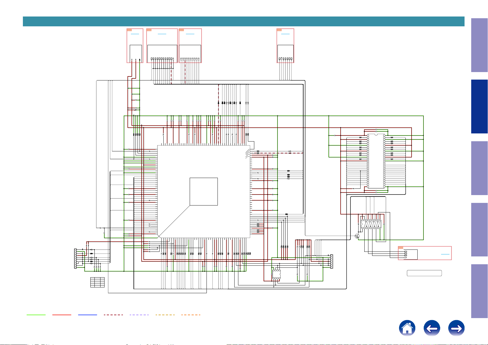
SCH06_ADI DSP1
3E
TO E3
TO
DA POWER
TO 8U-310223(5/19)
DGND
DA3.3V
DA1.1V-1
4D
TO D4
TO AUDIO PLD
TO 8U-310223(4/19)
DSP1INfs
DSP1IN64fs
DSP1_CLKIN
DSP1IN256fs
INPUT
INPUT
INPUT
INPUT
DSP1INS/SL
DSP1INF/FL
DSP1INSWC/C
INPUT
INPUT
INPUT
DSP1INRSV/SW
DSP1INRSV/FR
DSP1INSB/SR
INPUT
INPUT
INPUT
INPUT
All Ref.No. has been described in the parts list are four digits.
But there are less than four digits of printed Ref.No. on the PCB, and they have become four digits after the header by adding "0" in the parts list.
E7
TO 7E
TO DSP2
TO 8U-310223(7/19) TO 8U-310223(2/19)
DSP1INLR
DSP1_FLAG3
OUTPUT
DSP1OUT2INfs
DSP1OUT2IN64fs
OUTPUT
OUTPUT
OUTPUT
DSP1OUT2INS
DSP1OUT2INCSW
DSP1OUT2INF
DSP1OUT2INFH
DSP1OUT2INSB
OUTPUT
OUTPUT
OUTPUT
OUTPUT
DSP1OUT2INFW
DSP1OUT2INRSV
DSP1OUT2INRSV1
OUTPUT
OUTPUT
OUTPUT
2B
TO B2
TO CPU
DSPI_CLK
OUTPUT
INPUT
DSP_MISO
DSP_MOSI
DSP1_CS
INPUT
INPUT
INPUT
DSP1_FLAG0
INPUT
DSP_RST
INPUT
DSP1_WRITE
Caution in
servicing
TCK
GND
TDO
Vcc
TMS
TRST
EMU0
EMU1
TDI
GND
N101
OPEN
1
2
3
4
5
6
7
8
9
10
R122
OPEN
R102
4.7K
DSP1_FLAG3
DSP1INLR
DSP1INRSV/SW
DSP1INRSV/FR
DSP1INSB/SR
DSP1INS/SL
DSP1INSWC/C
DSP1INF/FL
DSP1IN256fs
DSP1INfs
DSP1IN64fs
DSP1_CLKIN
DSP_RST
DSP1_FLAG3
DSP1_FLAG0
DSP1_CLKIN
C9600
L102
NFM18PS105R0J3
0.1
C9601
NFM18PS105R0J3
L101
0.1
C9602
100/6.3
4.7Kx4
4.7Kx4
4.7Kx4
4.7Kx4
2
5678341
R141
R141
R141
R141
C105
1000P
R187
82
82
R189
0.1
C106
DSP1TRST
DSP1EMU0
DSP1D0
DSP1D1
DSP1D2
DSP1D3
DSP1TDO
DSP1D4
C108
0.1
DSP1D5
DSP1D6
C110
0.1
DSP1D7
DSP1TDI
DSP1SDCLK
47
1000P
1000P
1000P
0.1
DSP1D8
DSP1D9
DSP1D10
DSP1TCK
DSP1D11
DSP1D12
DSP1D14
DSP1D13
DSP1D15
DSP1WE
DSP1RAS
DSP1TMS
DSP1CAS
R111
R105
33
R106
33
33
R108
R123
4.7K
R107 4.7K
R128 4.7K
R129 4.7K
R112
OPEN
R130 OPEN
33
R103
0
OPEN
C100
DSP1TCK
DSP1TDO
DSP1TMS
DSP1TRST
DSP1EMU0
DSP1TDI
C107
C109
C114
C115
R12733R12433R12633R125
emi
normal
OPEN
3333R124
33
R125
OPEN
R126
1k
OPENR127
33
0.1
0.1
1000P
C120
C119
C117
4.7KR182
126
127
128
129
130
131
132
AMI_RD-
133
VDD_INT
ADDR16
ADDR15
ADDR14
134
135
136
137
138
139
140
141
142
143
144
145
146
147
148
149
150
151
152
153
154
155
156
157
158
159
160
161
162
163
164
165
166
167
168
169
170
171
172
173
174
175
176
177
VDD_EXT
VDD_INT
AMI_WR-
FLAG0
FLAG1
FLAG2
MLBCLK
FLAG3
MLBDAT
MLBDO
VDD_EXT
MLBSIG
VDD_INT
TRSTMLBSO
EMUDATA0
DATA1
DATA2
DATA3
TDO
DATA4
VDD_EXT
DATA5
DATA6
VDD_INT
DATA7
TDI
SDCLK
VDD_EXT
DATA8
DATA9
DATA10
TCK
DATA11
DATA12
DATA14
DATA13
VDD_INT
DATA15
SDWESDRASRESET-
TMS
SDCASVDD_INT
MS0-
SDDQM
SDCKE4VDD_INT5CLK_CFG16ADDR07BOOT_CFG08VDD_EXT9ADDR110ADDR211ADDR312ADDR413ADDR514BOOT_CFG115GND16ADDR617ADDR7
GND
1
2
3
33
OPEN
33x4
33x4
33x4
7 8
5 6
3 4
R116
R143
R143
R143
R113
0.1
C125
DSP1A0
DSP1DQM
DSP1SDCKE
DSP1CE0
124
125
ADDR19
33x4
1 2
R143
DSP1A1
DSP1OUT2INFW
DSP1OUT2INSB
DSP1OUT2INFH
DSP1OUT2INS
DSP1OUT2INF
DSP1OUT2INRSV1
DSP1OUT2INCSW
DSP1OUT2INRSV
DSP1OUT2INfs
0.1
0.1
1000P
1000P
C130
C131
C129
C132
4.7K
4.7K
R109
R183
113
114
115
116
117
118
119
120
121
MS1-
ADDR23
ADDR22
ADDR21
VDD_INT
VDD_INT
VDD_INT
VDD_EXT
WDT_CLKO
WDT_CLKIN
U101
ADSP-21487KSWZ-4B(xxxx-1)
1000P
C122
123
ADDR20
VDD_INT
DSP1OUT2IN64fs
0.1
C155
122
DSP1
ADDR821ADDR922CLK_CFG023VDD_INT24CLKIN25XTAL26ADDR1027SDA1028VDD_EXT29VDD_INT30ADDR1131ADDR1232ADDR1733ADDR1334VDD_INT35ADDR1836RESETOUT-/RUNRSTIN-37VDD_INT38DPI_P0139DPI_P0240DPI_P0341VDD_INT42DPI_P0543DPI_P0444DPI_P06
18NC19NC20
33x4
33x4
33x4
33x4
33x4
33x4
33x4
5 6
1 2
3 4
R144
R144
DSP1A4
DSP1A5
7 8
R145
R145
DSP1A7
DSP1A6
3 4
R145
DSP1A8
7 8
5 6
R144
R144
DSP1A2
DSP1A3
0.1
C121
110
111
112
THD_P
VDD_THD
33x4
1 2
R145
0.1
1000P
C140
C139
DSP1A9
0.1
C135
107
108
109
GND
THD_M
VDD_INT
AMI_ACK
56
R101
DSP1_CLKIN
1000P
1000P
C152
C136
4.7KR110
105
106
BOOT_CFG2
33
R115
0.1
C145
DSP1SDA10
DSP1INLR
103
104
DAI_P11
VDD_EXT
VDD_INT
33x4
7 8
R146
1000P
C146
DSP1A11
DSP1INF/FL
DSP1INSB/SR
0.1
C165
100
101
102
DAI_P12
DAI_P15
VDD_INT
33x4
33x4
3 4
5 6
R146
R146
DSP1A17
DSP1A12
DSP1INfs
DSP1INSWC/C
DSP1OUT2INfs
DSP1OUT2INFW
DSP1OUT2INCSW
DSP1OUT2IN64fs
82
R13182R13282R13382R134
33x4R150
33x4
33x4
7 8
5 6
1 2
R146
R150
0.1
1000P
C148
C150
DSP1A18
DSP1IN256fs
1000P
C156
DAI_P09
DAI_P05
DAI_P06
VDD_INT
VDD_EXT
33x4R150
3 4
0.1
C149
DSP1OUT2INFH
0.1
1000P
C168
C163
82x4
12
R114
89
90
91
VDD_EXT92DAI_P2093VDD_INT94DAI_P0895DAI_P1496DAI_P0497DAI_P1898DAI_P1799DAI_P16
VDD_INT
DAI_P10
VDD_INT
DAI_P02
DAI_P01
DAI_P19
DAI_P13
DAI_P07
VDD_EXT
WDTRSTO-
VDD_INT
VDD_INT
VDD_INT
VDD_EXT
DAI_P03
DPI_P14
DPI_P13
DPI_P12
DPI_P11
DPI_P10
DPI_P09
VDD_INT
DPI_P07
DPI_P08
82x4
82x4
33x4R150
56
1 2
R104
R104
DSP1OUT2INSB
82x4
34
R114
88
R114
87
R114
86
85
84
83
NC
82
NC
81
NC
80
NC
79
NC
78
77
R167
76
75
74
R168
73
72
71
NC
70
69
NC
68
67
NC
66
NC
65
64
NC
63
NC
62
61
NC
60
NC
59
NC
58
NC
57
56
NC
55
54
53
52
R117
51
R152
50
2
R152
49
4
48
R152
47
R152
46
45
VDD_EXT
82x4
82x4
783412
R104
R104
82x4
56
82x4
78
82
82
47
10Kx4
1
10Kx4
3
10Kx4
56
10Kx4
78
C167
C164
C166
C182
C171
C170
C179
C147
C180
1000P
1000P
1000P
1000P
0.1
C183
DSP1_CS
DSP_MISO
DSP_MOSI
DSPI_CLK
0.1
0.1
0.1
1000P
0.1
4.7Kx4
4.7Kx4
4.7Kx4
341256
R155
R155
R155
1
2
3
4
CS#
WP#
GND
SO/SIO1
SCLK
SI/SIO0
HOLD#
VCC
5
6
7
8
U102
MX25L1606EM2I-12G
DSP1_WRITE
DSP1_FLAG0
DSP_RST
DSP1OUT2INRSV1
DSP1OUT2INF
DSP1INRSV/FR
DSP1OUT2INRSV
DSP1IN64fs
DSP1INS/SL
DSP1OUT2INS
DSP1INRSV/SW
4.7Kx4
78
R155
DSP1_CS
DSPI_CLK
DSP_MISO
DSP_MOSI
4.7K
4.7K
4.7Kx4
R153
R118
R156
OPEN
R119
4.7Kx4
123456
R156
DSP1_WRITE
4.7Kx4
4.7Kx4
78
R156
R156
R135
100
OPEN
R120
SF_SO_DSP1
SF_SI_DSP1
SF_CS_DSP1
SF_CK_DSP1
C191
N102
OPEN
Electrical Mechanical Repair Information Updating
C192
1000P
C185
1000P
DSP1D0
R175
2
DSP1D1
R175
4
DSP1D2
R175
6
DSP1D3
R175
8
DSP1D4
R177
2
DSP1D5
R177
4
DSP1D6
R177
6
DSP1D7
R177
8
DSP1DQM
DSP1WE
DSP1CAS
DSP1RAS
DSP1CE0
DSP1A17
DSP1A18
DSP1SDA10
DSP1A0
DSP1A1
DSP1A2
DSP1A3
R181
4.7K
4.7KR121
Q101
KRC402E-RTK
1
SCK
2
GND
3
MOSI
4
VCC
5
CS
6
MISO
7
GND
ADI DSP1
1
VDD
56x4
1
2
DQ0
3
VDDQ
56x4
3
4
DQ1
56x4
5
5
DQ2
6
VSSQ
56x4
7
7
DQ3
56x4
1
8
DQ4
9
VDDQ
56x4
3
DQ5
10
56x4
5
DQ6
11
VSSQ
12
56x4
7
DQ7
13
VDD
14
LDQM
15
/WE
16
/CAS
17
/RAS
18
/CS
19
BS0
20
BS1
21
A10/AP
22
A0
23
A1
24
A2
25
A3
26
VDD
27
C186
C193
SF_SI_DSP1
SF_CK_DSP1
1OE21A132Y441A252Y361A372Y281A492Y1
1
0.1
VSS
DQ15
VSSQ
DQ14
DQ13
VDDQ
DQ12
DQ11
VSSQ
DQ10
DQ9
VDDQ
DQ8
VSS
UDQM
CLK
CKE
A12
A11
VSS
0.1
1000P
SF_CS_DSP1
11
2A1121Y4132A2141Y3152A3161Y2172A4181Y1192OE20VCC
GND
10
54
DSP1D15
R176
56x4
1
2
53
52
DSP1D14
R176
56x4
3
4
51
DSP1D13
56x4
R176
5
6
50
49
DSP1D12
R176
56x4
7
8
48
DSP1D11
R178
56x4
1
2
47
46
DSP1D10
R178
56x4
3
4
45
DSP1D9
56x4
R178
5
6
44
43
DSP1D8
R178
56x4
7
8
42
41
40
NC
A9
A8
A7
A6
A5
A4
39
38
37
36
35
34
33
32
31
30
29
28
U103
A3V56S40GTP-60
SF_SO_DSP1
DSP1DQM
DSP1SDCLK
DSP1SDCKE
DSP1A12
DSP1A11
DSP1A9
DSP1A8
DSP1A7
DSP1A6
DSP1A5
DSP1A4
0.1
TC74VHC244FT
C101
U104
E8
INPUT
DSP_SF_CK_WR
INPUT
DSP_SF_SI_WR
INPUT
DSP_SF_CS_WR
OUTPUT
DSP1_SF_SO_WR
8U-310223(6/19)
DIGITAL_UNIT
Condential
TO NET
MODULE CONNECT
TO 8U-310223(19/19)
TO 8E
GND LINE
POWER+ LINE
POWER- LINE
AUDIO SIGNAL
TMDS SIGNAL
ANALOG VIDEO
DIGITAL VIDEO
15
Page 16
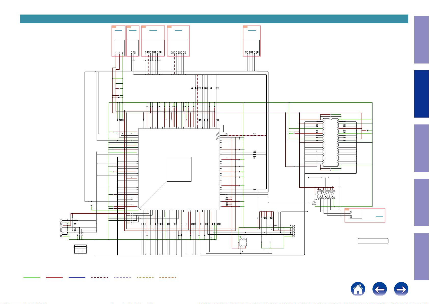
SCH07_ADI DSP2
N201
OPEN
TCK
1
GND
2
TDO
3
Vcc
4
5
TMS
6
TRST
EMU0
7
EMU1
8
TDI
9
GND
10
R222
OPEN
R202
4.7K
R225
R226
33
R22433R22533R22633R227
normal
3333R224
33
33
DSP_RST
R203
emi
OPEN
OPEN
1k
OPENR227
0
C201 OPEN
DSP2TCK
DSP2TDO
DSP2TMS
DSP2TRST
DSP2EMU0
DSP2TDI
All Ref.No. has been described in the parts list are four digits.
But there are less than four digits of printed Ref.No. on the PCB, and they have become four digits after the header by adding "0" in the parts list.
Caution in
servicing
Electrical Mechanical Repair Information Updating
C247
C239
C241
C248
C243
C242
C230
C246
C245
C249
0.1
C258
1000P
1000P
1000P
1000P
1000P
4
GND
SI/SIO0
5
1B
TO B1
TO CPU
DSP2_CS
DSP_MOSI
DSP_MISO
DSPI_CLK
DSP2_FLAG0
INPUT
INPUT
INPUT
INPUT
INPUT
OUTPUT
DSP2_CS
DSP2_FLAG0
DSP_RST
DSPI_CLK
DSP_MISO
DSP_MOSI
0.1
0.1
0.1
0.1
0.1
1
2
3
CS#
WP#
SO/SIO1
VCC
HOLD#
SCLK
6
7
8
U202
MX25L1606EM2I-12G
DSP2_WRITE
DSP_RST
DSP2_FLAG3
INPUT
BIDIRECT
DSP2_FLAG3
DSP2_WRITE
DSP3INRSV
DSP3INF
DSP1OUT2INFH
DSP1OUT2INRSV
DSP1OUT2IN64fs
DSP1OUT2INS
DSP3INS
DSP1OUT2INFW
DSP2_CS
DSPI_CLK
DSP_MISO
DSP_MOSI
4.7K
4.7K
R255
R218
OPEN
R219
4.7K
R253
4.7Kx4
4.7Kx4
123456
R256
R256
DSP2_WRITE
4.7Kx4
4.7Kx4
78
R256
R256
R235
100
OPEN
R220
SF_CK_DSP2
SF_SO_DSP2
SF_CS_DSP2
SF_SI_DSP2
C250
C251
R281
N202
OPEN
C252
1000P
C253
0.1
1
VDD
54
DSP2D0
56x4
R275
1
2
DSP2D1
56x4
R275
3
4
DSP2D2
56x4
R275
5
6
DSP2D3
R275
56x4
7
8
DSP2D4
56x4
DSP2D5
DSP2D6
DSP2D7
DSP2DQM
DSP2WE
DSP2CAS
DSP2RAS
DSP2CE0
DSP2A17
DSP2A18
DSP2SDA10
DSP2A0
DSP2A1
DSP2A2
DSP2A3
R277
R277
R277
R277
1
2
56x4
3
4
56x4
5
6
56x4
7
8
0.1
1000P
4.7K
4.7KR221
1OE21A132Y441A252Y361A372Y281A492Y1
1
Q201
KRC402E-RTK
1
SCK
2
GND
3
MOSI
4
VCC
5
CS
6
MISO
7
GND
ADI DSP2
2
DQ0
3
VDDQ
4
DQ1
5
DQ2
6
VSSQ
7
DQ3
8
DQ4
9
VDDQ
DQ5
10
DQ6
11
VSSQ
12
DQ7
13
VDD
14
LDQM
15
/WE
16
/CAS
17
/RAS
18
/CS
19
BS0
20
BS1
21
A10/AP
22
A0
23
A1
24
A2
25
A3
26
VDD
27
C254
C255
SF_CK_DSP2
SF_SI_DSP2
VSS
DQ15
VSSQ
DQ14
DQ13
VDDQ
DQ12
DQ11
VSSQ
DQ10
DQ9
VDDQ
DQ8
VSS
UDQM
CLK
CKE
A12
A11
VSS
0.1
1000P
SF_CS_DSP2
11
2A1121Y4132A2141Y3152A3161Y2172A4181Y1192OE20VCC
GND
10
DSP2D15
R276
56x4
8
7
53
52
DSP2D14
R276
56x4
6
5
51
DSP2D13
R276
56x4
4
3
50
49
DSP2D12
R276
56x4
2
1
48
DSP2D11
R278
56x4
8
7
47
46
DSP2D10
R278
56x4
6
5
45
DSP2D9
R278
56x4
4
3
44
43
DSP2D8
56x4
R278
1 2
42
41
40
NC
A9
A8
A7
A6
A5
A4
DSP2DQM
39
DSP2SDCLK
38
DSP2SDCKE
37
DSP2A12
36
DSP2A11
35
DSP2A9
34
DSP2A8
33
DSP2A7
32
DSP2A6
31
DSP2A5
30
DSP2A4
29
28
U203
A3V56S40GTP-60
SF_SO_DSP2
TC74VHC244FT
U204
F0
INPUT
DSP_SF_CK_WR
INPUT
DSP_SF_SI_WR
INPUT
DSP_SF_CS_WR
OUTPUT
DSP2_SF_SO_WR
8U-310223(7/19)
DIGITAL_UNIT
Condential
1000P
C257
TO
NET
TO 0F
MODULE
CONNECT
TO 8U-310223(19/19)
5D
4E
TO E4
TO
DA POWER
TO 8U-310223(4/19) TO 8U-310223(6/19)
TO 8U-310223(5/19)
DGND
DA3.3V
DA1.1V-2
DSP2_FLAG3
DSP2_FLAG0
L202
L201
C9615
NFM18PS105R0J3
0.1
C9616
NFM18PS105R0J3
0.1
C9617
100/6.3
4.7Kx4
4.7Kx4
4.7Kx4
4.7Kx4
2
5678341
R241
R241
R241
R241
1000P
C202
R292
R293
0.1
C203
DSP2TRST
DSP2EMU0
DSP2D0
DSP2D1
DSP2D2
DSP2D3
DSP2TDO
DSP2D4
C205
0.1
DSP2D5
DSP2D6
C209
0.1
DSP2D7
DSP2TDI
DSP2SDCLK
R211
DSP2D8
DSP2D9
DSP2D10
DSP2TCK
DSP2D11
DSP2D12
DSP2D14
DSP2D13
C206
1000P
DSP2D15
DSP2WE
R205
DSP2RAS
R206
DSP2TMS
DSP2CAS
1000P
0.1
R208
R223
R207
R228
R216
R286
R287
R212
C207
C208
TO D5
TO AUDIO
PLD
DSP2_FLAG3
DSP2_CLKIN
DSP2IN256fs
INPUT
INPUT
OUTPUT
DSP2IN256fs
DSP2_FLAG3
DSP2_CLKIN
133
82
134
135
136
137
82
138
139
140
141
142
143
144
145
146
147
148
149
150
151
152
153
154
155
156
157
158
47
159
160
161
162
163
164
165
166
167
168
169
170
33
171
33
172
173
174
33
175
176
4.7K
4.7K
4.7K
4.7K
OPEN
OPEN
OPEN
7E
TO E7
DSP1OUT2INCSW
DSP1OUT2INS
DSP1OUT2INF
DSP1OUT2INfs
DSP1OUT2IN64fs
INPUT
INPUT
INPUT
INPUT
INPUT
INPUT
DSP1OUT2IN64fs
DSP1OUT2INfs
DSP1OUT2INF
DSP1OUT2INCSW
DSP1OUT2INS
DSP1OUT2INSB
0.1
0.1
1000P
C215
C211
C210
4.7K
R248
125
126
127
128
129
130
131
132
AMI_RD-
VDD_INT
ADDR19
ADDR16
ADDR15
ADDR14
VDD_EXT
VDD_INT
AMI_WR-
FLAG0
FLAG1
FLAG2
MLBCLK
FLAG3
MLBDAT
MLBDO
VDD_EXT
MLBSIG
VDD_INT
TRSTMLBSO
EMUDATA0
DATA1
DATA2
DATA3
TDO
DATA4
VDD_EXT
DATA5
DATA6
VDD_INT
DATA7
TDI
SDCLK
VDD_EXT
DATA8
DATA9
DATA10
TCK
DATA11
DATA12
DATA14
DATA13
VDD_INT
DATA15
SDWESDRASRESET-
TMS
SDCASVDD_INT
177
MS0-
SDDQM
SDCKE4VDD_INT5CLK_CFG16ADDR07BOOT_CFG08VDD_EXT9ADDR110ADDR211ADDR312ADDR413ADDR514BOOT_CFG115GND16ADDR617ADDR7
GND
1
2
3
33
33x4
33x4
33x4
7 8
5 6
3 4
R243
R243
R243
R213
0.1
C213
DSP2A0
DSP2DQM
DSP2SDCKE
DSP2CE0
E9
TO 8U-310223(8/19) TO 8U-310223(2/19)
DSP3IN64fs
DSP1OUT2INRSV1
DSP1OUT2INRSV
DSP1OUT2INFW
DSP1OUT2INSB
DSP1OUT2INFH
INPUT
INPUT
INPUT
INPUT
OUTPUT
OUTPUT
DSP3INfs
DSP1OUT2INFW
DSP1OUT2INRSV1
DSP1OUT2INRSV
0.1
1000P
C217
C236
120
121
122
123
ADDR23
ADDR22
ADDR21
ADDR20
VDD_INT
0.1
C216
119
VDD_EXT
4.7K
R209
117
118
WDT_CLKO
WDT_CLKIN
DSP3IN64fs
1000P
C219
4.7K
R247
115
116
MS1-
VDD_INT
0.1
C221
114
DSP1OUT2INFH
124
ADSP-21487KSWZ-4B(xxxx-2)
DSP2
18NC19NC20
33x4
33x4
33x4
33x4
33x4
33x4
33x4
5 6
7 8
1 2
3 4
5 6
7 8
1 2
R245
R245
R244
R244
R244
R244
R243
DSP2A7
DSP2A1
DSP2A4
DSP2A2
DSP2A3
DSP2A6
DSP2A5
TO 9E
TO DSP3TO DSP1
DSP3INCSW
DSP3INfs
DSP3INS
DSP3INF
DSP3INRSV
DSP3INFW
DSP3INFH
DSP3INSB
OUTPUT
OUTPUT
OUTPUT
OUTPUT
OUTPUT
OUTPUT
OUTPUT
DSP3INFW
DSP3INFH
DSP3INSB
DSP3INS
DSP3INCSW
DSP3INF
DSP3INRSV
DSP3INFW
DSP3INFH
DSP3INCSW
DSP1OUT2INF
100
DAI_P12
DSP3INfs
33x4
7 8
R284
0.1
C231
DSP3IN64fs
33x4
5 6
R284
33x4
1 2
R246
DSP2A18
DSP1OUT2INfs
DSP1OUT2INCSW
33x4
33x4
3 4
1 2
R284
R284
33x4
33x4
7 8
5 6
R250
R250
1000P
C233
DSP2IN256fs
1000P
C237
DAI_P09
DAI_P05
DAI_P06
VDD_INT
VDD_EXT
33x4R250
3 4
0.1
C232
91
VDD_EXT92DAI_P2093VDD_INT94DAI_P0895DAI_P1496DAI_P0497DAI_P1898DAI_P1799DAI_P16
33x4
1 2
R250
WDTRSTO-
1000P
C244
33x4
7 8
R214
89
90
VDD_INT
DAI_P10
VDD_INT
DAI_P02
DAI_P01
DAI_P19
DAI_P13
DAI_P07
VDD_EXT
VDD_INT
VDD_INT
VDD_INT
VDD_EXT
DAI_P03
DPI_P14
DPI_P13
DPI_P12
DPI_P11
DPI_P10
DPI_P09
VDD_INT
DPI_P07
DPI_P08
4.7Kx4
4.7Kx4
R251
R251
DSP1OUT2INSB
DSP1OUT2INRSV1
0.1
C218
1000P
1000P
C226
C225
0.1
C240
0.1
1000P
C214
C220
4.7K
R210
101
102
103
104
105
106
107
108
109
110
111
112
113
GND
THD_M
VDD_INT
VDD_INT
THD_P
VDD_THD
AMI_ACK
VDD_INT
BOOT_CFG2
DAI_P11
VDD_EXT
VDD_INT
DAI_P15
VDD_INT
U201
ADDR821ADDR922CLK_CFG023VDD_INT24CLKIN25XTAL26ADDR1027SDA1028VDD_EXT29VDD_INT30ADDR1131ADDR1232ADDR1733ADDR1334VDD_INT35ADDR1836RESETOUT-/RUNRSTIN-37VDD_INT38DPI_P0139DPI_P0240DPI_P0341VDD_INT42DPI_P0543DPI_P0444DPI_P06
56
33
33x4
33x4
3 4
1 2
R245
R245
DSP2A9
DSP2A8
0.1
C222
1000P
C223
R215
R201
DSP2_CLKIN
DSP2SDA10
33x4
7 8
R246
1000P
C212
DSP2A11
33x4
33x4
3 4
5 6
R246
R246
DSP2A12
DSP2A17
DSP3INSB
33x4
5 6
R214
NC
NC
NC
NC
NC
NC
NC
NC
NC
NC
NC
NC
NC
NC
NC
NC
VDD_EXT
4.7Kx4
4.7Kx4
56
R251
R251
88
R214
87
3 4
33x4
R214
33x4
86
1 2
85
84
83
82
81
80
79
78
77
76
75
74
73
R268
33
72
71
70
69
68
67
66
65
64
63
62
61
60
59
58
57
56
55
54
53
47
R217
52
51
10Kx4
R252
50
12
R252
10Kx4
49
34
48
10Kx4
R252
47
5
6
R252
46
10Kx4
7
8
45
783412
GND LINE
POWER+ LINE
POWER- LINE
AUDIO SIGNAL
TMDS SIGNAL
ANALOG VIDEO
DIGITAL VIDEO
16
Page 17
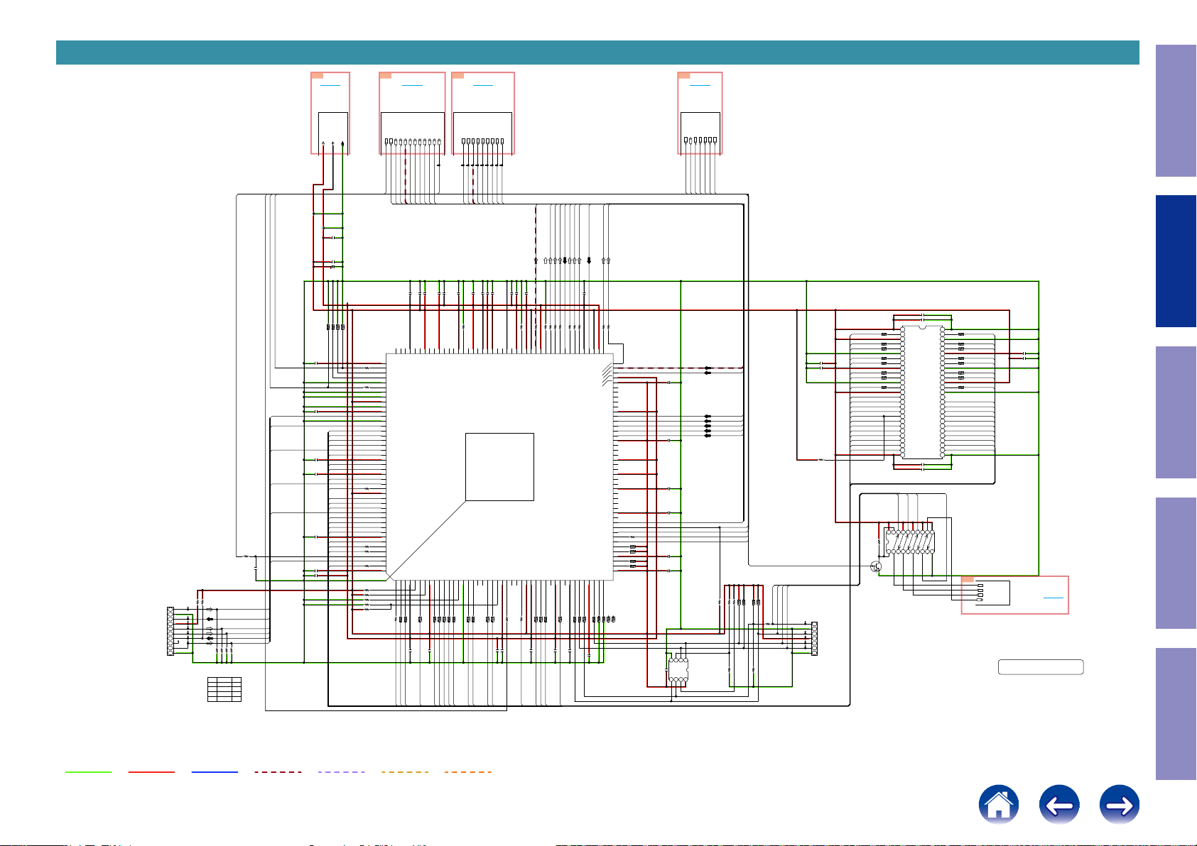
SCH08_ADI DSP3
N301
OPEN
TCK
1
GND
2
TDO
3
Vcc
4
5
TMS
6
TRST
EMU0
7
EMU1
8
TDI
9
GND
10
R304
OPEN
4.7K
R302
R325
R326
33
R32433R32533R32633R327
normal
3333R324
33
33
DSP_RST
R303
emi
OPEN
OPEN
1k
OPENR327
0
OPEN
C301
DSP3TCK
DSP3TDO
DSP3TMS
DSP3TRST
DSP3EMU0
DSP3TDI
DSP3_FLAG0
DSP3_FLAG3
DSP3_CLKIN
5E
TO E5
TO
DA POWER
TO 8U-310223(5/19)
DA3.3V
DA1.1V-2
L302
C9620
L301
0.1
NFM18PS105R0J3
C9621
NFM18PS105R0J3
0.1
C9622
100/6.3
4.7Kx4
4.7Kx4
4.7Kx4
5678341
R341
R341
R341
C302
1000P
C303
0.1
DSP3TRST
DSP3EMU0
DSP3D0
DSP3D1
DSP3D2
DSP3D3
DSP3TDO
DSP3D4
0.1
C305
DSP3D5
DSP3D6
C309
0.1
DSP3D7
DSP3TDI
DSP3SDCLK
DSP3D8
DSP3D9
DSP3D10
DSP3TCK
DSP3D11
DSP3D12
DSP3D14
DSP3D13
C330
1000P
DSP3D15
DSP3WE
DSP3RAS
DSP3TMS
DSP3CAS
C307
1000P
C308
0.1
DGND
4.7Kx4
2
R341
R380
R382
R311
R305
R306
R308
R323
R307
R322
R321
R312
6D
TO D6
TO AUDIO PLD
TO 8U-310223(4/19)
DSP3IN256fs
DSP3_CLKIN
DSP3OUTF
DSP3OUT64fs
DSP3OUTfs
INPUT
INPUT
OUTPUT
OUTPUT
OUTPUT
DSP3IN256fs
DSP3OUT64fs
DSP3OUTfs
DSP3OUTF
DSP3_CLKIN
130
131
132
AMI_RD-
133
VDD_INT
ADDR14
82
134
AMI_WR-
FLAG0
135
FLAG1
136
FLAG2
137
MLBCLK
82
138
FLAG3
139
MLBDAT
140
MLBDO
141
VDD_EXT
142
MLBSIG
143
VDD_INT
144
TRST-
145
MLBSO
146
EMU-
147
DATA0
148
DATA1
149
DATA2
150
DATA3
151
TDO
152
DATA4
153
VDD_EXT
154
DATA5
155
DATA6
156
VDD_INT
157
DATA7
158
TDI
47
159
SDCLK
160
VDD_EXT
161
DATA8
162
DATA9
163
DATA10
164
TCK
165
DATA11
166
DATA12
167
DATA14
168
DATA13
169
VDD_INT
170
DATA15
33
171
SDWE-
33
172
SDRAS-
173
RESETTMS
174
SDCAS-
33
175
VDD_INT
176
177
MS0-
SDDQM
SDCKE4VDD_INT5CLK_CFG16ADDR07BOOT_CFG08VDD_EXT9ADDR110ADDR211ADDR312ADDR413ADDR514BOOT_CFG115GND16ADDR617ADDR7
GND
1
2
3
4.7K
4.7K
4.7K
4.7K
OPEN
33x4
33x4
33
7 8
5 6
R313
R343
R343
DSP3DQM
DSP3SDCKE
DSP3CE0
DSP3OUTS
DSP3OUTCSW1
OUTPUT
OUTPUT
DSP3OUTCSW1
DSP3OUTS
0.1
C311
128
129
ADDR15
VDD_INT
0.1
C313
DSP3OUTFH
DSP3OUTSB
OUTPUT
OUTPUT
OUTPUT
DSP3OUTFW
DSP3OUTFH
DSP3OUTSB
1000P
0.1
C310
C315
125
126
127
ADDR19
ADDR16
VDD_EXT
33x4
3 4
R343
1000P
C312
DSP3A0
DSP3OUTFW
DSP3OUTRSV
OUTPUT
OUTPUT
DSP3OUTRSV
DSP3_FLAG3
1000P
C317
123
124
ADDR20
33x4
33x4
7 8
1 2
R344
R343
DSP3A1
DSP3A2
All Ref.No. has been described in the parts list are four digits.
But there are less than four digits of printed Ref.No. on the PCB, and they have become four digits after the header by adding "0" in the parts list.
9E
TO E9
TO DSP2
TO 8U-310223(7/19)
DSP3_FLAG3
DSP3INCSW
DSP3INFH
DSP3INSB
DSP3INS
DSP3INF
DSP3IN64fs
DSP3INfs
INPUT
INPUT
INPUT
INPUT
INPUT
INPUT
INPUT
INPUT
DSP3INfs
DSP3INF
DSP3INCSW
DSP3INS
DSP3INSB
DSP3INFH
DSP3INFW
DSP3IN64fs
1000P
1000P
0.1
0.1
0.1
0.1
C316
C314
C319
C320
C321
C318
4.7K
R309
111
112
113
114
115
116
117
118
119
120
121
122
MS1-
ADDR23
ADDR22
ADDR21
VDD_INT
ADSP-21487KSWZ-4B(xxxx-3)
VDD_EXT
WDT_CLKO
WDT_CLKIN
VDD_INT
VDD_INT
VDD_INT
U301
VDD_THD
DSP3
ADDR821ADDR922CLK_CFG023VDD_INT24CLKIN25XTAL26ADDR1027SDA1028VDD_EXT29VDD_INT30ADDR1131ADDR1232ADDR1733ADDR1334VDD_INT35ADDR1836RESETOUT-/RUNRSTIN-37VDD_INT38DPI_P0139DPI_P0240DPI_P0341VDD_INT42DPI_P0543DPI_P0444DPI_P06
18NC19NC20
33x4
33x4
33x4
33x4
33x4
33x4
33x4
5 6
3 4
1 2
3 4
5 6
7 8
1 2
R345
R345
R344
R344
R344
R345
R345
0.1
C322
DSP3A7
DSP3A4
DSP3A3
DSP3A6
DSP3A5
DSP3A9
DSP3A8
DSP3INFW
DSP3INRSV
INPUT
DSP3INRSV
DSP3OUTF
0.1
1000P
1000P
C325
C326
C335
4.7K
33
R310
R35433R35733R35833R35933R34933R36033R36233R363
106
107
108
109
110
103
104
105
GND
THD_M
THD_P
DAI_P11
VDD_EXT
VDD_INT
VDD_INT
AMI_ACK
BOOT_CFG2
56
33x4
33
7 8
R316
R301
R346
1000P
1000P
C329
C323
DSP3_CLKIN
DSP3SDA10
DSP3A11
10K
R329
101
102
DAI_P15
VDD_INT
33x4
33x4
3 4
5 6
R346
R346
DSP3A17
DSP3A12
DSP3OUTS
100
DAI_P12
DSP3OUTfs
0.1
C331
DSP3INfs
DSP3OUT64fs
33
R361
33x4
1 2
R346
DSP3A18
DSP3OUTFW
DSP3OUTSB
DSP3OUTRSV
1000P
C337
33x4R350
33x4
33x4
3 4
7 8
5 6
R350
R350
1000P
C333
DSP3IN256fs
91
VDD_EXT92DAI_P2093VDD_INT94DAI_P0895DAI_P1496DAI_P0497DAI_P1898DAI_P1799DAI_P16
DAI_P09
DAI_P05
DAI_P06
VDD_INT
VDD_EXT
WDTRSTO-
33x4
1 2
R350
0.1
C332
DSP3OUTCSW1
89
90
VDD_INT
DAI_P10
VDD_INT
DAI_P02
DAI_P01
DAI_P19
DAI_P13
DAI_P07
VDD_EXT
VDD_INT
VDD_INT
VDD_INT
VDD_EXT
DAI_P03
DPI_P14
DPI_P13
DPI_P12
DPI_P11
DPI_P10
DPI_P09
VDD_INT
DPI_P07
DPI_P08
4.7Kx4
4.7Kx4
56
R351
R351
DSP3OUTFH
88
87
86
85
84
83
NC
82
NC
81
NC
80
NC
79
NC
78
77
76
75
74
73
72
71
NC
70
69
NC
68
67
NC
66
NC
65
64
NC
63
NC
62
61
NC
60
NC
59
NC
58
NC
57
56
NC
55
54
53
R317
52
51
R352
50
R352
49
48
R352
47
R352
46
45
VDD_EXT
4.7Kx4
4.7Kx4
783412
R351
R351
0B
TO B0
TO CPU
TO 8U-310223(2/19)
DSP_RST
DSP3_WRITE
DSP3_CS
DSP3_FLAG0
DSP_MOSI
DSP_MISO
DSPI_CLK
INPUT
INPUT
INPUT
INPUT
INPUT
INPUT
OUTPUT
DSP3_WRITE
DSP3_CS
DSP3_FLAG0
DSPI_CLK
DSP_MISO
DSP_RST
DSP_MOSI
Caution in
servicing
Electrical Mechanical Repair Information Updating
C352
1000P
C353
0.1
1
VDD
54
DSP3D0
56x4
R375
1
2
DSP3D1
56x4
R375
3
4
DSP3D2
56x4
R375
5
6
DSP3D3
R375
56x4
7
8
DSP3D4
0.1
SF_SO_DSP3
SF_CS_DSP3
SF_SI_DSP3
SF_CK_DSP3
C350
C351
R381
N302
OPEN
1000P
4.7K
1
SCK
2
GND
3
MOSI
4
VCC
5
CS
6
MISO
7
GND
DSP3INF
DSP3IN64fs
4.7K
R355
1
2
CS#
SO/SIO1
VCC
HOLD#
7
8
U302
MX25L1606EM2I-12G
DSP3INCSW
DSP3INS
DSP3INSB
DSP3INFW
DSP3INFH
DSP3INRSV
DSP3_CS
DSPI_CLK
DSP_MISO
DSP_MOSI
4.7K
4.7K
4.7Kx4
R318
R353
R356
OPEN
R319
4.7Kx4
123456
R356
DSP3_WRITE
4.7Kx4
4.7Kx4
78
R356
R356
R335
100
OPEN
R320
C339
1000P
C348
0.1
1000P
C344
C346
1000P
47
10Kx4
12
10Kx4
34
0.1
C345
10Kx4
5
6
10Kx4
7
8
0.1
C349
3
4
0.1
WP#
GND
SCLK
SI/SIO0
5
6
C358
56x4
R377
1
2
DSP3D5
56x4
R377
3
4
DSP3D6
56x4
R377
5
6
DSP3D7
56x4
R377
7
8
DSP3DQM
DSP3WE
DSP3CAS
DSP3RAS
DSP3CE0
DSP3A17
DSP3A18
DSP3SDA10
DSP3A0
DSP3A1
DSP3A2
DSP3A3
4.7K
1OE21A132Y441A252Y361A372Y281A492Y1
R332
1
Q301
KRC402E-RTK
ADI DSP3
2
DQ0
3
VDDQ
4
DQ1
5
DQ2
6
VSSQ
7
DQ3
8
DQ4
9
VDDQ
DQ5
10
DQ6
11
VSSQ
12
DQ7
13
VDD
14
LDQM
15
/WE
16
/CAS
17
/RAS
18
/CS
19
BS0
20
BS1
21
A10/AP
22
A0
23
A1
24
A2
25
A3
26
VDD
27
C354
C355
SF_CK_DSP3
SF_SI_DSP3
VSS
DQ15
VSSQ
DQ14
DQ13
VDDQ
DQ12
DQ11
VSSQ
DQ10
DQ9
VDDQ
DQ8
VSS
UDQM
CLK
CKE
A12
A11
VSS
0.1
1000P
SF_CS_DSP3
11
2A1121Y4132A2141Y3152A3161Y2172A4181Y1192OE20VCC
GND
10
DSP3D15
R376
56x4
8
7
53
52
DSP3D14
R376
56x4
6
5
51
DSP3D13
R376
56x4
4
3
50
49
DSP3D12
R376
56x4
2
1
48
DSP3D11
R378
56x4
8
7
47
46
DSP3D10
R378
56x4
6
5
45
DSP3D9
R378
56x4
4
3
44
43
DSP3D8
56x4
R378
1 2
42
41
40
NC
A9
A8
A7
A6
A5
A4
39
38
37
36
35
34
33
32
31
30
29
28
SF_SO_DSP3
U303
A3V56S40GTP-60
DSP3DQM
DSP3SDCLK
DSP3SDCKE
DSP3A12
DSP3A11
DSP3A9
DSP3A8
DSP3A7
DSP3A6
DSP3A5
DSP3A4
TC74VHC244FT
U304
F1
INPUT
DSP_SF_CK_WR
INPUT
DSP_SF_SI_WR
INPUT
DSP_SF_CS_WR
OUTPUT
DSP3_SF_SO_WR
8U-310223(8/19)
DIGITAL_UNIT
Condential
0.1
C356
1000P
C357
TO
NET
TO 1F
MODULE
CONNECT
TO 8U-310223(19/19)
GND LINE
POWER+ LINE
POWER- LINE
AUDIO SIGNAL
TMDS SIGNAL
ANALOG VIDEO
DIGITAL VIDEO
17
Page 18
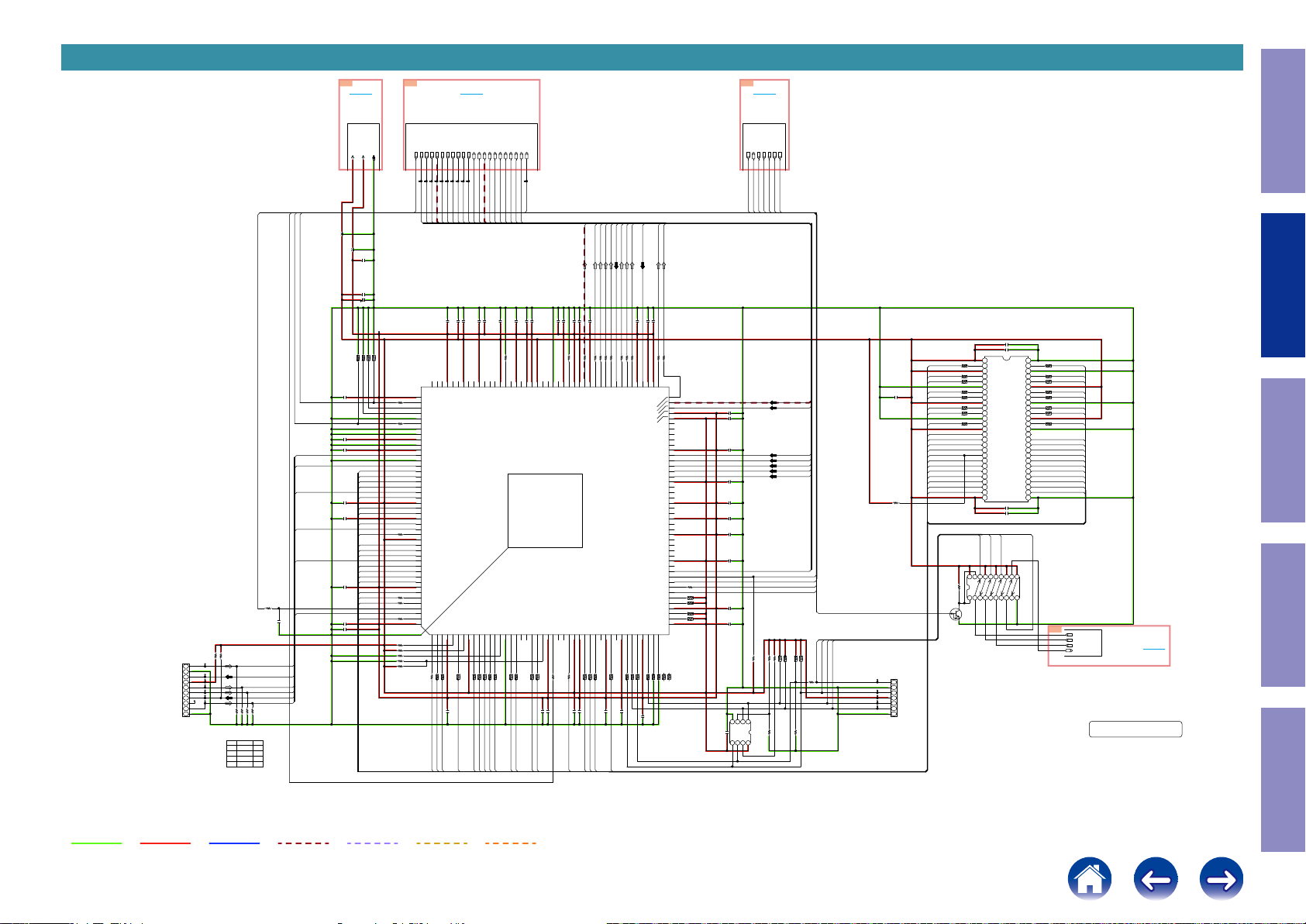
SCH09_ADI DSP4
6E
TO E6
TO
DA POWER
TO 8U-310223(5/19)
7D
TO D7
TO AUDIO PLD
TO 8U-310223(4/19)
All Ref.No. has been described in the parts list are four digits.
But there are less than four digits of printed Ref.No. on the PCB, and they have become four digits after the header by adding "0" in the parts list.
9A
TO A9
TO CPU
TO 8U-310223(2/19)
Caution in
servicing
TCK
GND
TDO
Vcc
TMS
TRST
EMU0
EMU1
TDI
GND
N401
OPEN
1
2
3
4
5
6
7
8
9
10
R442
OPEN
R402
4.7K
R424
R425
R426
R427
33
33
R424
R425
normal
331kOPEN
33
33
33
33
R426
33
R427
emi
OPEN
OPEN
DSP_RST
R403
0
OPEN
C401
DSP4TCK
DSP4TDO
DSP4TMS
DSP4TRST
DSP4EMU0
DSP4TDI
DSP4_FLAG0
DSP4_FLAG3
DSP4_CLKIN
L402
L401
NFM18PS105R0J3
NFM18PS105R0J3
C402
1000P
C404
1000P
C403
0.1
0.1
C405
C409
0.1
C412
1000P
C407
1000P
C408
0.1
DA3.3V
DA1.1V-1
C9630
0.1
C9632
0.1
C9631
100/6.3
8
6
4.7Kx4
4.7Kx4
7
5
R441
R441
DSP4TRST
DSP4EMU0
DSP4D0
DSP4D2
DSP4D3
DSP4TDO
DSP4D4
DSP4D5
DSP4D6
DSP4D7
DSP4TDI
DSP4SDCLK
DSP4D8
DSP4D9
DSP4D10
DSP4TCK
DSP4D11
DSP4D12
DSP4D14
DSP4D13
DSP4D15
DSP4WE
DSP4RAS
DSP4TMS
DSP4CAS
4
2
4.7Kx4
4.7Kx4
3
1
R441
R441
DGND
R482
R483
R411
R405
R406
R408
R423
R407
R422
R421
R412
DSP4INF
DSP4IN64fs
DSP4INfs
DSP4_CLKIN
DSP4IN256fs
DSP4INCSW
INPUT
INPUT
INPUT
INPUT
INPUT
INPUT
DSP4_CLKIN
DSP4IN256fs
DSP4IN64fs
DSP4INCSW
DSP4INF
DSP4INfs
130
131
132
AMI_RD-
133
VDD_INT
ADDR14
82
134
AMI_WR-
FLAG0
135
FLAG1
136
FLAG2
137
MLBCLK
82
138
FLAG3
139
MLBDAT
140
MLBDO
141
VDD_EXT
142
MLBSIG
143
VDD_INT
144
TRST-
145
MLBSO
146
EMU-
147
DATA0
148
DATA1
149
DATA2
150
DATA3
151
TDO
152
DATA4
153
VDD_EXT
154
DATA5
155
DATA6
156
VDD_INT
157
DATA7
158
TDI
47
159
SDCLK
160
VDD_EXT
161
DATA8
162
DATA9
163
DATA10
164
TCK
165
DATA11
166
DATA12
167
DATA14
168
DATA13
169
VDD_INT
170
DATA15
33
171
SDWE-
33
172
SDRAS-
173
RESETTMS
174
SDCAS-
33
175
VDD_INT
176
177
MS0-
SDDQM
SDCKE4VDD_INT5CLK_CFG16ADDR07BOOT_CFG08VDD_EXT9ADDR110ADDR211ADDR312ADDR413ADDR514BOOT_CFG115GND16ADDR617ADDR7
GND
1
2
3
4.7K
4.7K
4.7K
4.7K
OPEN
33
33x4
33x4
7 8
5 6
R413
R443
R443
DSP4SDCKE
DSP4DQM
DSP4CE0
DSP4INSB
DSP4INS
INPUT
INPUT
DSP4INSB
DSP4INS
0.1
C410
128
129
ADDR15
VDD_INT
0.1
C413
DSP4INFH
DSP4INFW
INPUT
INPUT
INPUT
DSP4INRSV
DSP4INFW
DSP4INFH
0.1
1000P
C414
C415
125
126
127
ADDR19
ADDR16
VDD_EXT
33x4
3 4
R443
DSP4A0
DSP4OUT64fs
DSP4INRSV
OUTPUT
OUTPUT
DSP4OUTfs
DSP4OUT64fs
1000P
C417
123
124
ADDR20
33x4
33x4
7 8
1 2
R444
R443
DSP4A2
DSP4A1
DSP4OUTS
DSP4OUTFW
DSP4_FLAG3
DSP4OUTSW2RSV
DSP4OUTRSV
DSP4OUTFH
DSP4OUTSB
DSP4OUTCSW1
DSP4OUTfs
DSP4OUTF
OUTPUT
OUTPUT
OUTPUT
OUTPUT
OUTPUT
OUTPUT
OUTPUT
OUTPUT
OUTPUT
DSP4OUTRSV
DSP4_FLAG3
DSP4OUTS
DSP4OUTSB
DSP4OUTCSW1
DSP4OUTFH
DSP4OUTFW
DSP4OUTSW2RSV
DSP4OUTF
0.1
1000P
1000P
0.1
0.1
C416
C418
C419
C420
C421
4.7K
R409
ADDR21
VDD_INT
ADSP-21487KSWZ-4B(xxxx-4)
VDD_EXT
WDT_CLKO
WDT_CLKIN
VDD_INT
VDD_INT
VDD_INT
U401
VDD_THD
111
112
113
114
115
116
117
118
119
120
121
122
MS1-
ADDR23
ADDR22
DSP4
ADDR821ADDR922CLK_CFG023VDD_INT24CLKIN25XTAL26ADDR1027SDA1028VDD_EXT29VDD_INT30ADDR1131ADDR1232ADDR1733ADDR13
18NC19NC20
33x4
33x4
33x4
33x4
33x4
33x4
33x4
3 4
1 2
3 4
5 6
1 2
7 8
5 6
R444
R444
R445
R445
R445
R445
R444
0.1
C422
DSP4A5
DSP4A6
DSP4A3
DSP4A4
DSP4A7
DSP4A8
DSP4A9
109
110
THD_M
THD_P
56
R401
1000P
C423
DSP4_CLKIN
DSP4_CS
DSP_MOSI
DSPI_CLK
DSP_MISO
DSP4_WRITE
DSP4_FLAG0
DSP_RST
INPUT
INPUT
INPUT
INPUT
INPUT
INPUT
OUTPUT
DSP4_CS
DSP4_FLAG0
DSPI_CLK
DSP_MISO
DSP_MOSI
DSP4_WRITE
DSP_RST
DSP4OUTS
DSP4INfs
DSP4OUTF
DSP4OUTFW
DSP4OUTSB
DSP4OUTRSV
33
33
33
R404
R400
R465
33x4
33x4
5 6
7 8
R450
R450
1000P
C433
DSP4IN256fs
1000P
C438
DAI_P09
DAI_P05
DAI_P06
VDD_INT
VDD_EXT
33x4
3 4
R450
0.1
C432
0.1
C440
91
VDD_EXT92DAI_P2093VDD_INT94DAI_P0895DAI_P1496DAI_P0497DAI_P1898DAI_P1799DAI_P16
33x4
1 2
R450
WDTRSTO-
DSP4OUTCSW1
1000P
C437
33
R414
89
90
VDD_INT
DAI_P10
VDD_INT
DAI_P02
DAI_P01
DAI_P19
DAI_P13
DAI_P07
VDD_EXT
VDD_INT
VDD_INT
VDD_INT
VDD_EXT
DAI_P03
DPI_P14
DPI_P13
DPI_P12
DPI_P11
DPI_P10
DPI_P09
VDD_INT
DPI_P07
DPI_P08
4.7Kx4
4.7Kx4
56
34
R451
R451
DSP4OUTFH
33
R415
88
87
86
85
84
83
NC
82
NC
81
NC
80
NC
79
NC
78
77
76
75
74
73
72
71
NC
70
69
NC
68
67
NC
66
NC
65
64
NC
63
NC
62
61
NC
60
NC
59
NC
58
NC
57
56
NC
55
54
53
R417
52
51
R452
50
R452
49
48
R452
47
R452
46
45
VDD_EXT
4.7Kx4
4.7Kx4
12
78
R451
R451
C447
C439
1000P
1000P
C441
C448
C442
C443
1000P
C444
1000P
C446
1000P
47
10Kx4
12
10Kx4
34
C445
10Kx4
5
6
10Kx4
7
8
C449
0.1
C458
U402
MX25L1606EM2I-12G
0.1
0.1
0.1
0.1
0.1
3
4
WP#
GND
SCLK7HOLD#
SI/SIO0
5
6
Electrical Mechanical Repair Information Updating
C452
1000P
C453
0.1
1
VDD
54
DSP4D0
56x4
R475
1
2
DSP4D1
56x4
R475
3
4
DSP4D2
56x4
R475
5
6
DSP4D3
R475
56x4
7
8
DSP4D4
0.1
DSP4INF
DSP4INCSW
DSP4INS
DSP4INSB
DSP4IN64fs
DSP4INFW
DSP4INFH
DSP4INRSV
DSP4_CS
DSPI_CLK
DSP_MISO
DSP_MOSI
DSP4_WRITE
4.7K
4.7K
4.7K
4.7Kx4
4.7Kx4
4.7Kx4
4.7Kx4
56
34
78
SF_CK_DSP4
SF_SO_DSP4
SF_CS_DSP4
R456
R456
R456
R456
OPEN
R420
R435
100
SF_SI_DSP4
R418
R455
R453
1
2
OPEN
CS#
SO/SIO1
VCC
8
R419
C450
R481
N400
OPEN
4.7K
1
SCK
2
GND
3
MOSI
4
VCC
5
CS
6
MISO
7
GND
56x4
R477
1
2
DSP4D5
56x4
R477
3
4
DSP4D6
56x4
R477
5
6
DSP4D7
56x4
R477
7
8
DSP4DQM
DSP4WE
DSP4CAS
DSP4RAS
DSP4CE0
DSP4A17
DSP4A18
DSP4SDA10
DSP4A0
DSP4A1
DSP4A2
DSP4A3
4.7KR432
1OE21A132Y441A252Y361A372Y281A492Y1
1
Q401
KRC402E-RTK
ADI DSP4
2
DQ0
3
VDDQ
4
DQ1
5
DQ2
6
VSSQ
7
DQ3
8
DQ4
9
VDDQ
DQ5
10
DQ6
11
VSSQ
12
DQ7
13
VDD
14
LDQM
15
/WE
16
/CAS
17
/RAS
18
/CS
19
BS0
20
BS1
21
A10/AP
22
A0
23
A1
24
A2
25
A3
26
VDD
27
C454
C455
SF_CK_DSP4
SF_SI_DSP4
VSS
DQ15
VSSQ
DQ14
DQ13
VDDQ
DQ12
DQ11
VSSQ
DQ10
DQ9
VDDQ
DQ8
VSS
UDQM
CLK
CKE
A12
A11
VSS
0.1
1000P
SF_CS_DSP4
11
2A1121Y4132A2141Y3152A3161Y2172A4181Y1192OE20VCC
GND
10
NC
A9
A8
A7
A6
A5
A4
DSP4D15
R476
56x4
8
7
53
52
DSP4D14
R476
56x4
6
5
51
DSP4D13
R476
56x4
4
3
50
49
DSP4D12
R476
56x4
2
1
48
DSP4D11
R478
56x4
8
7
47
46
DSP4D10
R478
56x4
6
5
45
DSP4D9
R478
56x4
4
3
44
43
DSP4D8
56x4
R478
1 2
42
41
40
DSP4DQM
39
DSP4SDCLK
38
DSP4SDCKE
37
DSP4A12
36
DSP4A11
35
DSP4A9
34
DSP4A8
33
DSP4A7DSP4D1
32
DSP4A6
31
DSP4A5
30
DSP4A4
29
28
U403
A3V56S40GTP-60
SF_SO_DSP4
TC74VHC244FT
U404
F2
INPUT
TO
DSP_SF_CK_WR
INPUT
DSP_SF_SI_WR
NET
INPUT
DSP_SF_CS_WR
MODULE
OUTPUT
DSP4_SF_SO_WR
CONNECT
TO 8U-310223(19/19)
8U-310223(9/19)
DIGITAL_UNIT
Condential
TO 2F
DSP4OUTfs
DSP4OUT64fs
DSP4OUTSW2RSV
1000P
0.1
0.1
0.1
1000P
C426
C435
C425
C434
C436
33
33
33
33
33
4.7K
R464
R463
R462
R461
R428
R410
100
101
102
103
104
105
106
107
108
GND
VDD_INT
AMI_ACK
DAI_P12
DAI_P15
VDD_INT
DAI_P11
VDD_EXT
VDD_INT
BOOT_CFG2
VDD_INT35ADDR1836RESETOUT-/RUNRSTIN-37VDD_INT38DPI_P0139DPI_P0240DPI_P0341VDD_INT42DPI_P0543DPI_P0444DPI_P06
34
33x4
33
33x4
33x4
33x4
7 8
3 4125 6
1 2
R416
R446
R446
R446
R446
1000P
0.1
0.1
C430
C428
C431
DSP4SDA10
DSP4A12
DSP4A17
DSP4A18
DSP4A11
GND LINE
POWER+ LINE
POWER- LINE
AUDIO SIGNAL
TMDS SIGNAL
ANALOG VIDEO
DIGITAL VIDEO
18
Page 19
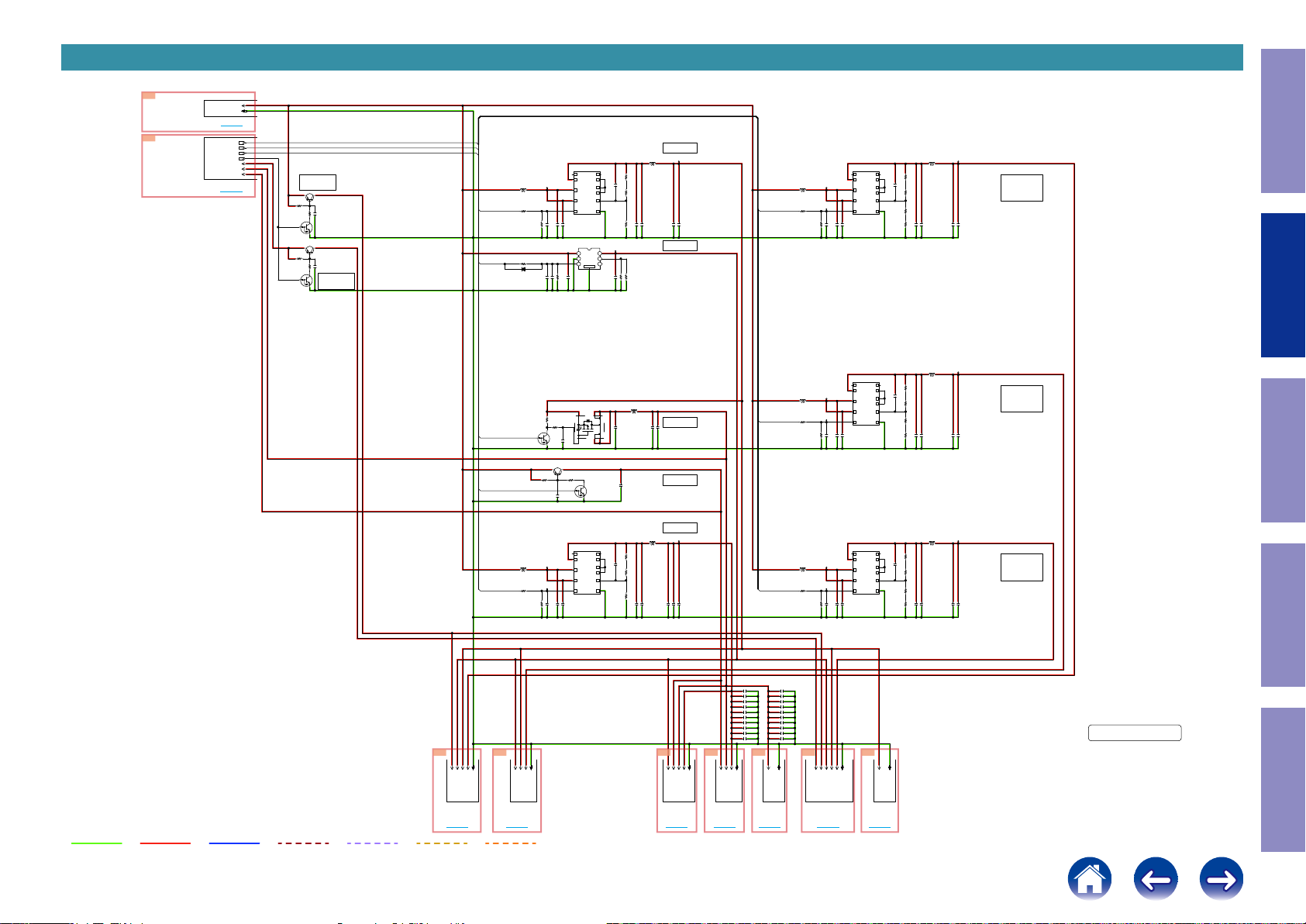
SCH10_HDMI SUPPLY
3A
TO
DIGITAL
CONNECT
TO 8U-310223(1/19)
7B
TO 8U-310223(2/19)
TO
CPU
D5V
DGND
TO A3
DV_POWER1
DV_POWER2
CEC_POWER1
CEC_POWER2
M3.3V
DV3.3V
DV5V
TO B7
All Ref.No. has been described in the parts list are four digits.
But there are less than four digits of printed Ref.No. on the PCB, and they have become four digits after the header by adding "0" in the parts list.
Caution in
servicing
INPUT
INPUT
INPUT
INPUT
CEC
STBY5V
Q3607
R3605
10K
2SA2018
R3611
C3617
3.3K
OPEN
Q3602
KRC404E-RTK
Q3608
R3606
2SA2018
10K
R3612
C3618
3.3K
OPEN
CEC
Q3606
STBY3.3V
KRC404E-RTK
DV_POWER1
DV_POWER2
CEC_POWER1
CEC_POWER1
DV_POWER1
DV_POWER1
L3600
BLM21PG221
R3656
10
R3601
22K
KDS160
D3601
Q3691
KRC404E-RTK
47K
R3600
R3691
10K
R3692
10K
0.1
C3600
OPEN
1608
C3605
R3694
Q3692
C3690
OPEN
10/6.3
C3629
1M
22/6.3
C3606
R3602
100K
1
11
9
7
6
1u
XCL212B082DR
C3608
NCP380HMUAJAATBG
6
5
4
1u
C3602
4
3
0.1
C3692
2SA2018
R3697
3.3K
47k/47k
NC
L2
PVIN
AVIN
CE
IN
GND
EN
Q3696
FDC608PZ
L1
GND
U3601
U3602
ILIM
FLAG#
7
Q3694
KRC404E-RTK
NC
LX
LX
FB
OUT
5
2
4
10
2
3
5
8
1
2
3
6
1
47K
R3620
330P
0
C3634
R3628
15K
R3621
1u
47K
OPEN
R3609
R3607
C3604
L3691
BLM21PG221
0.1
C3694
0.1
C3695
L3608
BLM21PG221
22/6.3
10/6.3
C3671
C3612
0.1
C3697
CEC3.3V
CEC5V
1000PC3699
DV3.3V
DV5V
0.1
1000P
C3682
C3679
CEC_POWER1CEC_POWER1
CEC_POWER1
L3616
BLM21PG221
R3655
10
47K
R3632
L3750
BLM21PG221
R3750
10
47K
R3752
0.1
C3650
0.1
C3750
10/6.3
C3659
C3665
10/6.3
C3752
1u
1u
C3754
NC
1
NC
4
L2
11
10
L1
2
LX
9
PVIN
3
LX
7
5
AVIN
FB
GND
8
6
CE
U3604
XCL212B082DR
NC
1
NC
4
L2
11
10
L1
2
LX
9
PVIN
3
LX
7
5
AVIN
FB
GND
8
6
CE
U3605
XCL212B082DR
1200P
C3674
1200P
C3756
R3641
R3643
R9221
R3642
R3754
R3755
R9220
R3756
6.2K
6.2K
15K
15K
6.2K
6.2K
15K
15K
L3622
BLM21PG221
22/6.3
10/6.3
C3767
C3766
L3752
BLM21PG221
22/6.3
10/6.3
C3760
C3758
0.1
1000P
C3769
C3768
0.1
1000P
C3764
C3762
CEC1.1V
for
HDMI SW1
CEC1.1V
for
HDMI SW2
Electrical Mechanical Repair Information Updating
GND LINE
POWER+ LINE
POWER- LINE
AUDIO SIGNAL
TMDS SIGNAL
DV1.8V
L3614
NC
1
NC
L2
11
0.1
C3603
C3615
10/6.3
9
7
6
1u
XCL212B082DR
C3623
PVIN
AVIN
CE
L1
GND
U3603
LX
LX
FB
L3606
BLM21PG221
R3659
DV_POWER2
10
47K
R3603
F3
TO HDMI SW1
TO 8U-310223(13/19) TO 8U-310223(14/19) TO 8U-310223(17/19)
TO 3F
ANALOG VIDEO
CEC5V
CEC3.3V
CEC_STBY5V
F4
DGND
CEC1.1V1
DGND
CEC5V
CEC3.3V
CEC1.1V2
TO HDMI SW2
TO 8U-310223(12/19) TO 8U-310223(11/19)
TO 4F
DIGITAL VIDEO
BLM21PG221
4
0
10
R3626
560P
2
3
68K
C3637
R3631
5
8
51K
R3627
C3627
10/6.3
C3633
22/6.3
0.1
OPEN
C3641
C3645
F5
DV5V
CEC5V
TO DEC
1000PC3649
DV3.3V
DV1.8V
DGND
C9034
C9035
C9036
C9037
C9038
C9039
C9040
C9041
C9042
C9043
DGND
DV5V
DV1.8V
DV3.3V
TO IP/OSD
OPEN
OPEN
OPEN
OPEN
OPEN
OPEN
OPEN
OPEN
OPEN
OPEN
L3751
BLM21PG221
R3751
CEC_POWER1
10
OPEN
C9024
OPEN
C9025
OPEN
C9026
OPEN
C9027
OPEN
C9028
OPEN
C9029
OPEN
C9030
OPEN
C9031
OPEN
C9032
OPEN
C9033
DGND
DV3.3V
TO VPLD
TO 8U-310223(16/19)
TO 5FF6TO 6FF7TO 7F
19
47K
0.1
1u
10/6.3
C3755
C3753
R3753
C3751
F8
DGND
CEC5V
CEC3.3V
CEC1.1V3
CEC_STBY5V
CEC_STBY3.3V
TO HDMI TX
TO 8FF9TO 9F
NC
1
NC
4
L2
11
10
L1
2
LX
9
PVIN
3
LX
7
5
AVIN
FB
GND
8
6
CE
U3606
XCL212B082DR
CEC3.3V
TO eARC
TO 8U-310223(18/19)
1200P
C3757
DGND
R3757
R3758
R9219
R3759
6.2K
6.2K
15K
15K
L3753
BLM21PG221
0.1
1000P
22/6.3
10/6.3
C3765
C3763
C3761
C3759
HDMI SUPPLY
CEC1.1V3
CEC1.1V
for
HDMI Tx
8U-310223(10/19)
DIGITAL_UNIT
Condential
Page 20
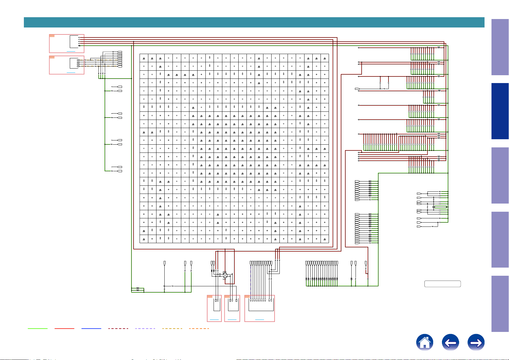
SCH11_DECODER
5F
TO 8U-310223(10/19)
5A
TO 8U-310223(1/19)
TO
HDMI
SUPPLY
TO
DIGITAL
CONNECT
TO F5
TO A5
CEC5V
DV5V
DV3.3V
DV1.8V
DGND
DECIN_Y
DECIN_CR
DECIN_CB
DECIN_V
1V
R2000
R2001
R2002
R2003
All Ref.No. has been described in the parts list are four digits.
But there are less than four digits of printed Ref.No. on the PCB, and they have become four digits after the header by adding "0" in the parts list.
Caution in
servicing
BLM21PG221
TX_VDD33
ACPLL_LF
TX_AVDD
TX_PVDD
TX_PLVDD
VIN1
VIN2
VIN3
VIN13
HS_IN1/TRI7
VS_IN1/TRI8
HS_IN2/TRI5
VS_IN2/TRI6
VIN10
VIN11
ACIN_5L
ACIN_5R
ACIN_4L
ACIN_4R
ACIN_3L
ACIN_3R
ACIN_2L
ACIN_2R
ACIN_1L
ACIN_1R
AC_MCLK
AC_LRCLK
AC_SDI
AC_SCLK
SPDIF_IN
TVDD
DVDDIO
AC_VDD
PVDD
VDD
CVDD
V_VDD
SDVDD
SAVDD
AC18
AC19
AB19
AA18
AA19
AA22
AA23
C2092 1000P
C2111 1000P
C2098 1000P
C2105 1000P
C2102 1000P
C2095 1000P
0.1
0.1
0.1
0.1
C2032 1000P
C2027
C2017
C2012
C2037 1000P
C2022
0.1
1000PC2052
C2062
0.1
C2020
R2060
R2060
R2060
R2059
R2060
R2059
R2059
R2059
R2078
R2079
R2058
R2058
R2058
R2058
R2057
R2057
R2057
R2062
R2057
R2063
R2054
R2054
R2054
R2054
R2064
0.1
0.1
C2025
C2030
3 4
7 8
5 6
7 8
1 2
1 2
3 4
5 6
1 2
3 4
5 6
7 8
1 2
3 4
5 6
7 8
1 2
3 4
7 8
5 6
0.1
0.1
C2034
C2040
4.7Kx4
4.7Kx4
4.7Kx4
4.7Kx4
4.7Kx4
4.7Kx4
4.7Kx4
4.7Kx4
4.7K
4.7K
47Kx4
47Kx4
47Kx4
47Kx4
47Kx4
47Kx4
47Kx4
47K
47Kx4
47K
47Kx4
47Kx4
47Kx4
47Kx4
47K
0.1
0.1
C2045
C2050
C2055 1000P
C2057 1000P
R2065
2.2K
C2060 1000P
C2059 1000P
C2067 1000P
C2063 1000P
C2071 1000P
C2074 1000P
4.7u
C2077
F20
0.1
C2015
U20
U23
U22
G23
G22
F23
F22
E23
E22
D23
D22
C23
C22
N3
N4
P3
P4
H3
0.1
0.1
C2085
C2082
OPEN.C2065
0.1
C2039
0.1
0.1
C2087
C2089
0.1
0.1
C2072
C2069
0.1
0.1
C2014
C2019
0.1
0.1
C2049
C2044
0.1
0.1
C2091
C2094
0.1
0.1
C2021
C2016
TX_RTERM.
VGA_SCL
VDD_EEPROM
EP_MISO
0.1
0.1
C2078
C2075
0.1
0.1
C2024
C2029
0.1
0.1
C2056
C2054
C2097 1000P
C2101 1000P
0.1
C2026
C2031 1000P
REFN
REFP
XTALP
XTALN
VREG
0.1
0.1
C2080
C2083
0.1
0.1
C2033
C2038
0.1
0.1
C2066
C2058
C2109 1000P
C2104 1000P
C2041 1000P
C2035 1000P
AC2
R22
R23
N23
N22
D14
D16
C8
H1
0.1
C2086
0.1
C2043
0.1
C2070
C2113 1000P
4.7u
C2046
0.1
C2000
SD_R
SD_B
SD_G
Y
R2017
150
470
CR
R2018
470
150
CB
150
R2019
470
CVBS
150
R2020
470
330
330
330
R2022
R2023
R2024
C2001
C2002
C2003 1000P
C2004
C2005
C2006
C2007
330
R2025
R2014
R2026
R2015
R2027
VIN8
W23
0.1
VIN9
W22
0.1
VIN7
Y23
SYNC2
AB21
0.1
VIN4
AC21
0.1
VIN5
AC22
0.1
VIN6
AB22
0.1
VIN12
U21
RXD_5V
D4
10K
DDCD_SCL
D12
RXC_5V
E4
10K
DDCC_SCL
D10
RXB_5V
F4
10K
DDCB_SCL
D8
RXA_5V
H4
10K
DDCA_SCL
D6
1
2 3 4 5 6 7 8
A2
A3
A4
A5
A6
A7
A1
2
3
DGND
B3
25
DGND
C3
48
CVDD
CVDD
D3
71
CVDD
CVDD
E3
94
CVDD
CVDD
F3
CVDD
CVDD
G3
TVDD
TVDD
H3
SPDIF_IN
SPDIF_IN
J3
SEL_EDID
K3
DVDDIO
DVDDIO
L3
INT1
M3
INT2
N3
AC_MCLK
AC_MCLK
P3
AC_SDI
AC_SDI
R3
TTX_MISO
TTX_MISO
T3
DGND
U3
DGND
V3
DGND
W3
DGND
Y3
DGND
AA3
TX_AVDD
TX_AVDD
AB3
TX_PLVDD
TX_PLVDD
AC3
TX_VDD33
TX_VDD33
GND
26
GND
49
72
95
118
141
164
187
NC
210
233
NC
256
NCNCNC
279
302
325
348
GND
371
GND
TX_DDC_SCL
TX_DDC_SCL
394
GND
TX_DDC_SDA
TX_DDC_SDA
417
GND
440
GND
463
486
509
RXB_2+
B4
RXB_2-
C4
GND
DGND
D4
RXD_5V
RXD_5V
E4
RXC_5V
RXC_5V
F4
RXB_5V
RXB_5V
G4
TVDD
TVDD
H4
RXA_5V
RXA_5V
J4
RESET
RESET
K4
DVDDIO
DVDDIO
L4
SDA
SDA
M4
SCL
SCL
N4
AC_LRCLK
AC_LRCLK
P4
AC_SCLK
AC_SCLK
R4
TTX_CSB
T4
GND
DGND
U4
V4
W4
TX_HPD
TX_HPD
Y4
GND
DGND
AA4
GND
DGND
AB4
SDVDD
SDVDD
AC4
SDVDD
SDVDD
4
RXB_1+
B5
27
RXB_1-
C5
50
GND
DGND
D5
73
VGA_5V
NC NC
96
119
142
165
188
211
234
257
280
303
326
349
372
395
418
Y5
441
442
SDRAM_A7
AA5
464
465
SDRAM_A9
AB5
487
488
SDRAM_A11
AC5
510
511
SDRAM_A8
28
51
74
1
GND
GND
A
DGND
DGND
B1
B2
24
ARC_A
HPA_A
B
NC NC NC NC NC NC NC NC NC NC NC NC NC NC NC NC NC NC NC
C1
C2
47
RXA_C+
RXA_C-
C
NC NC
D1
D2
70
RXA_0+
RXA_0-
D
NC NC
E1
E2
93
RXA_1+
RXA_1-
E
NC NC
F1
F2
116
117
RXA_2+
RXA_2-
F
NC NC
G1
G2
139
140
TVDD
TVDD
G
TVDD
TVDD
H1
H2
162
163
EP_MISO
EP_MOSI
H
NC
EP_MISO
J1
J2
185
186
EP_CS
EP_SCK
J
NCNC
K1
K2
208
209
GND
GND
K
DGND
DGND
L1
L2
232
231
HA_AP5
HA_SCLK
L
NC
HA_SCLK
M1
M2
254
255
HA_AP4
HA_AP3/INT3
M
N1
N2
277
278
HA_AP2
HA_AP1
N
NCNC
P1
P2
300
301
HA_AP0
HA_MCLKOUT
P
NCNC
R1
R2
323
324
TTX_SCLK
TTX_MOSI
R
NCNC NC
T1
T2
346
347
DVDDIO
DVDDIO
T
DVDDIO
DVDDIO
U1
U2
369
370
TX_AVDD
TX_AVDD
U
TX_AVDD
TX_AVDD
V1
V2
392
393
TX_2+
TX_2-
V
TX_2-
TX_2+
W1
W2
415
416
TX_1+
TX_1-
W
TX_1-
TX_1+
Y1
Y2
438
439
TX_0+
TX_0-
Y
TX_0+
TX_0-
AA1
AA2
461
462
TX_C+
TX_C-
AA
TX_C+
TX_C-
AB1
AB2
484
485
GND
TX_PVDD
AB
TX_PVDD
DGND
AC1
AC2
507
508
GND
TX_RTERM
AC
DGND
TX_RTERM.
5
RXB_0+
B6
RXB_0-
C6
D6
DDCA_SCL
DDCA_SCL
Y6
SDRAM_A3
AA6
SDRAM_A5
AB6
SDRAM_A6
AC6
SDRAM_A4
GND
DGND
6
RXB_C+
B7
29
RXB_C-
C7
52
D7
75
DDCA_SDA
G7
H7
J7
K7
L7
M7
N7
P7
R7
T7
U7
Y7
443
SDRAM_A10
AA7
466
SDRAM_A1
AB7
489
SDRAM_A2
AC7
512
SDRAM_A0
A8
7
B8
30
C8
53
GND
VDD_EEPROM
VDD_EEPROM
DGND
D8
76
G8
145
GND
DGND
H8
168
GND
DGND
J8
191
GND
DGND
K8
214
VDD
VDD
L8
237
VDD
VDD
M8
260
VDD
VDD
N8
283
VDD
VDD
P8
306
VDD
VDD
R8
329
VDD
VDD
T8
352
VDD
VDD
U8
375
VDD
VDD
Y8
444
SDRAM_BA0
AA8
467
SDRAM_BA1
AB8
490
SDRAM_CAS
NC NCNC NC NC
AC8
513
NCNC NCNC NC NC
10 11 12 13 14 15 16
9
A9
A10
TVDD
TVDD
B9
TVDD
TVDD
C9
TVDD
TVDD
D9
DDCB_SDA
G9
CVDD
CVDD
H9
DGND
J9
DGND
K9
DGND
L9
DGND
M9
DGND
N9
DGND
P9
DGND
R9
DGND
T9
DGND
U9
VDD
Y9
SDRAM_CKE
AA9
SDRAM_WE
AB9
SDRAM_RAS
AC9
SDRAM_CK
A11
9
10
RXC_2+
RXC_1+
B10
B11
32
33
RXC_2-
RXC_1-
C10
C11
55
56
TVDD
TVDD
TVDD
TVDD
D10
D11
78
79
DDCC_SCL
DDCC_SDA
DDCC_SCL
G10
G11
147
148
149
CVDD
CVDD
CVDD
CVDD
H10
H11
170
171
193
216
239
262
285
308
331
354
377
446
469
492
515
GND
DGND
J10
GND
DGND
K10
GND
DGND
L10
GND
DGND
M10
GND
DGND
N10
GND
DGND
P10
GND
DGND
R10
GND
DGND
T10
GND
DGND
U10
VDD
VDD
Y10
GND
DGND
AA10
GND
DGND
AB10
SDRAM_VREF
SDRAM_VREF
AC10
SDRAM_CK
172
GND
DGND
J11
194
195
GND
DGND
K11
217
218
GND
DGND
L11
240
241
GND
DGND
M11
263
264
GND
DGND
N11
286
287
GND
DGND
P11
309
310
GND
DGND
R11
332
333
GND
DGND
T11
355
356
GND
DGND
U11
378
379
VDD
VDD
Y11
447
448
SDRAM_DQ6
SDRAM_DQ6
AA11
470
471
SDRAM_DQ4
SDRAM_DQ4
AB11
493
494
SDVDD
SDVDD
AC11
516
517
SDVDD
SDVDD
GND
GND
GND
GND
GND
GND
GND
GND
GND
VDD
8
ARC_B
31
HPA_B
54
77
DDCB_SCL
DDCB_SCL
146
TEST1
NC
169
GND
DGND
192
GND
DGND
215
GND
DGND
238
GND
DGND
261
GND
DGND
284
GND
DGND
307
GND
DGND
330
GND
DGND
353
GND
DGND
376
VDD
VDD
445
NCNCNC NC NC
468
NCNCNC NC NC
491
514
SDRAM_CS
A12
11
RXC_0+
NC NCNC NCNC NC NC NCNC NC NCNC NC NC NC
B12
34
RXC_0-
C12
57
TVDD
TVDD
D12
80
DDCD_SCL
DDCD_SCL
G12
CVDD
CVDD
H12
GND
DGND
J12
GND
DGND
K12
GND
DGND
L12
GND
DGND
M12
GND
DGND
N12
GND
DGND
P12
GND
DGND
R12
GND
DGND
T12
GND
DGND
U12
VDD
VDD
Y12
SDRAM_DQ7
SDRAM_DQ7
AA12
SDRAM_DQ5
SDRAM_DQ5
AB12
SDRAM_LDQSN
NC
AC12
SDRAM_LDQS
SDRAM_LDQS
A13
A14
A15
A16
A17
12
13
14
36
59
82
151
174
197
220
243
266
289
312
335
358
381
450
473
496
519
ARC_C
B14
HPA_C
C14
TVDD
TVDD
D14
VREG
VREG
G14
CVDD
CVDD
H14
GND
DGND
J14
GND
DGND
K14
GND
DGND
L14
GND
DGND
M14
GND
DGND
N14
GND
DGND
P14
GND
DGNDDGND
R14
GND
DGND
T14
GND
DGND
U14
TEST2
NC
Y14
SDRAM_DQ8
SDRAM_DQ8
AA14
SDRAM_DQ11
SDRAM_DQ11
AB14
SDRAM_DQ10
SDRAM_DQ10
AC14
SDRAM_DQ9
SDRAM_DQ9
37
60
83
152
175
198
221
244
267
290
313
336
359
382
451
474
497
520
GND
DGND
B15
GND
DGND
C15
GND
DGND
D15
GND
DGND
G15
CVDD
CVDD
H15
GND
DGND
J15
GND
DGND
K15
GND
DGND
L15
GND
DGND
M15
GND
DGND
N15
GND
DGND
P15
GND
DGND
R15
GND
DGND
T15
GND
DGND
U15
GND
DGND
Y15
SDRAM_UDQS
SDRAM_UDQS
AA15
SDRAM_UDQSN
NC
AB15
SDRAM_DQ12
SDRAM_DQ12
AC15
SDRAM_DQ15
SDRAM_DQ15
15
38
61
84
153
176
199
222
245
268
291
314
337
360
383
452
475
498
521
RXC_C+
B13
35
RXC_C-
C13
58
TVDD
TVDD
D13
81
DDCD_SDA
G13
150
CVDD
CVDD
H13
173
GND
DGND
J13
196
GND
DGND
K13
219
GND
DGND
L13
242
GND
DGND
M13
265
GND
DGND
N13
288
GND
DGND
P13
311
GND
R13
334
GND
DGND
T13
357
GND
DGND
U13
380
VDD
VDD
Y13
449
SDRAM_DQ0
SDRAM_DQ0
AA13
472
SDRAM_DQ2
SDRAM_DQ2
AB13
495
SDRAM_DQ3
SDRAM_DQ3
AC13
518
SDRAM_DQ1
SDRAM_DQ1
RXD_2+
B16
RXD_2-
C16
TVDD
TVDD
D16
VGA_SCL
VGA_SCL
G16
GND
DGND
H16
GND
DGND
J16
GND
DGND
K16
GND
DGND
L16
GND
DGND
M16
GND
DGND
N16
GND
DGND
P16
GND
DGND
R16
GND
DGND
T16
GND
DGND
U16
GND
DGND
Y16
SDVDD
SDVDD
AA16
SDVDD
SDVDD
AB16
SDRAM_DQ14
SDRAM_DQ14
AC16
SDRAM_DQ13
SDRAM_DQ13
A18
16
17
RXD_1+
B17
B18
39
40
RXD_1-
C17
C18
62
63
TVDD
TVDD
D17
D18
85
86
VGA_SDA
NCNC NCNC
G17
154
155
GND
DGND
H17
177
178
GND
DGND
J17
200
201
GND
DGND
K17
223
224
GND
DGND
L17
246
247
GND
DGND
M17
269
270
GND
DGND
N17
292
293
GND
DGND
P17
315
316
GND
DGND
R17
338
339
GND
DGND
T17
362
361
GND
DGND
U17
384
385
GND
DGND
Y17
Y18
453
454
SAVDD
SAVDD
AA17
AA18
476
477
GND
HS_IN1/TR17
DGND
AB17
AB18
499
500
GND
DGND
AC17
AC18
522
523
GND
DGND
RXD_0+
RXD_0-
TVDD
TVDD
TVDD
TVDD
455
TRI1
NCNCNC
478
HS_IN1/TRI7
501
SYNC1
524
VIN1
VIN1
18
41
64
87
VS_IN1/TR18
A19
RXD_C+
B19
RXD_C-
C19
TVDD
TVDD
D19
AC_VDD
AC_VDD
Y19
TRI2
AA19
VS_IN1/TRI8
AB19
VIN3
VIN3
AC19
VIN2
VIN2
20191817 21 2322
A20
19
20
ARC_D
B20
42
43
HPA_D
C20
65
66
GND
DGND
D20
88
89
AC_VDD
AC_VDD
E20
112
GND
DGND
F20
135
ACPLL_LF
ACPLL_LF
G20
158
AC_VDD
AC_VDD
H20
181
GND
DGND
J20
204
AC_VDD
AC_VDD
K20
227
AC_VDD
AC_VDD
L20
250
AC_VDD
AC_VDD
M20
273
AC_VDD
AC_VDD
N20
296
PVDD
PVDD
P20
319
GND
DGND
R20
342
GND
DGND
T20
365
V_VDD
V_VDD
U20
388
VIN13
VIN13
V20
411
V_VDD
V_VDD
W20
434
GND
DGND
Y20
456
457
GND
DGND
AA20
479
480
GND
DGND
AB20
502
503
GND
DGND
AC20
525
526
GND
DGND
U2000
A21
B21
C21
D21
E21
F21
G21
H21
J21
K21
L21
M21
N21
P21
R21
T21
U21
V21
W21
Y21
AA21
AB21
AC21
ADV7850KBCZ-5
GND
DGND
GND
DGND
GND
DGND
AC_VDD
AC_VDD
113
GND
DGND
136
GND
DGND
159
GND
DGND
182
GND
DGND
205
GND
DGND
228
AC_VDD
AC_VDD
251
AC_VDD
AC_VDD
274
GND
DGND
297
PVDD
PVDD
320
GND
DGND
343
GND
DGND
366
V_VDD
V_VDD
389
VIN12
VIN12
412
V_VDD
V_VDD
435
VOUT2
NC
458
VOUT1
NC NC
481
TRI3
NC
504
SYNC2
SYNC2
527
VIN4
VIN4
21
44
67
90
A22
GND
DGND
B22
ACOUT_R
C22
ACIN_1R
ACIN_1R
D22
ACIN_2R
ACIN_2R
E22
ACIN_3R
ACIN_3R
F22
ACIN_4R
ACIN_4R
G22
ACIN_5R
ACIN_5R
H22
AC_FILTA
J22
AC_ISET
NC NC
K22
AC_DOUT_R
L22
HPOUT_R
NC NC
M22
GND
DGND
N22
XTALN
XTALN
P22
GND
DGND
R22
REFN
REFN
T22
V_VDD
V_VDD
U22
VIN11
VIN11
V22
V_VDD
V_VDD
W22
VIN9
VIN9
Y22
SYNC3
AA22
HS_IN2/TR5
HS_IN2/TRI5
AB22
VIN6
VIN6
AC22
VIN5
VIN5
114
137
160
183
206
229
252
275
298
321
344
367
390
413
436
459
482
505
528
22
45
68
91
A23
B23
ACOUT_L
C23
ACIN_1L
ACIN_1L
D23
ACIN_2L
ACIN_2L
E23
ACIN_3L
ACIN_3L
F23
ACIN_4L
ACIN_4L
G23
ACIN_5L
ACIN_5L
H23
VREF_AC
J23
AC_FILTD
K23
AC_DOUT_L
L23
HPOUT_L
M23
N23
XTALP
XTALP
P23
R23
T23
V_VDD
V_VDD
U23
VIN10
VIN10
V23
V_VDD
V_VDD
W23
Y23
AA23
VS_IN2/TR6
VS_IN2/TRI6
AB23
AC23
GND
DGND
NCNC
NCNC
GND
DGND
GND
DGND
REFP
REFP
VIN8
VIN8
VIN7
VIN7
TRI4
NC
GND
DGND
23
46
69
92
115
138
161
184
207
230
253
276
299
322
345
368
391
414
437
460
483
506
529
C2115 1000P
C2042 1000P
0.1
C2088
OPEN.C2011
0.1
C2048
0.1
C2073
C2116 1000P
0.1
C2110
R2066
OPEN
C2118 1000P
C2047 1000P
0.1
C2090
0.1
C2013
0.1
C2053
C2076 1000P
4.7u
C2119
C2114 1000P
4.7u
C2125 1000P
C2122 1000P
C2120 1000P
C2129
BLM21PG221
BLM21PG221
4.7u
0.1
4.7u
C2068
C2064 1000P
C2061
C2051
BLM21PG221
0.1
4.7u
C2130
C2096 1000P
C2099 1000P
C2093
BLM21PG221
4.7u
0.1
C2023 1000P
C2028 1000P
C2018
C2106
BLM21PG221
4.7u
C2103 1000P
C2112
C2107 1000P
C2100 1000P
BLM21PG221
4.7u
C2108
C2084 1000P
C2081 1000P
C2079 1000P
BLM21PG221
BLM21PG221
BLM21PG221
0.1
4.7u
C2127 1000P
C2123
C2131
BLM21PG221
BLM21PG221
BLM21PG221
0.1
4.7u
4.7u
C2121
C2124 1000P
C2128
C2117
R2068
R2069
C2133
C2134
C2132
0.1
C2135
C2136
1 3
27MHz
X2000
C2137
C2138
C2139
R2071
C2140
OPEN
R2067
L2001
L2002
L2003
L2004
L2000
L2005
L2006
L2007
L2008
L2009
L2010
L2011
L2012
OPEN
470
OPEN
OPEN
OPEN
8P
10P
1u
0.1
10K
0.1
Electrical Mechanical Repair Information Updating
GND LINE
POWER+ LINE
POWER- LINE
AUDIO SIGNAL
10x4
R2031
3 4
R2031
10x4
7 8
TMDS SIGNAL
RESET
J4
R2034
1K
C2010
1000P
ANALOG VIDEO
HA_SCLK
TTX_MISO
R3
L2
10K
OPEN
R2077
R2038
DIGITAL VIDEO
SCL
SDA
M4
L4
10x4
10x4
10K
10K
5 6
1 2
R2031
R2031
R2032
R2033
G0
.AVSCL
.AVSDA
TO IP/OSD
TO 8U-310223(14/19)
TO 0G
Q2001
HN1K02FU
G
2
1
6
D
S
S
D
3
4
G
5
8B
AVSCL
TO CPU
TO 8U-310223(2/19)
TO B8
TX_0+
TX_C+
TX_C-
TX_2-
TX_2+
TX_0-
TX_1-
TX_1+
TX_DDC_SDA
TX_DDC_SCL
W4
Y1
V2
V1
Y2
W2
W1
V4
U4
AA1
AA2
G1
TX_1-
TX_0+
TX_0-
TX_C+
DE_RST
TX_C-
TO Tx
TO 8U-310223(17/19)
TO 1G
AVSDA
TX_1+
R2085
R2084
R2083
0
0
R2076
R2075
TX_2-
TX_2+
RXD_DDCCL
RXD_DDCDA
SDRAM_DQ0
Y13
4.7Kx4
4.7Kx4
12
78
R2050
R2053
SDRAM_DQ2
SDRAM_DQ1
AA13
AC13
4.7K
R2016
SDRAM_DQ3
AB13
4.7Kx4
4.7Kx4
34
R2051
R2050
SDRAM_DQ4
SDRAM_DQ5
AA11
AA12
4.7Kx4
78
R2051
SDRAM_DQ6
Y11
4.7Kx4
4.7Kx4
56
12
R2051
R2051
SDRAM_DQ8
SDRAM_DQ7
Y14
Y12
4.7Kx4
R2053
SDRAM_DQ9
AC14
4.7Kx4
4.7Kx4
7856563434
56
R2050
R2050
SDRAM_DQ11
SDRAM_DQ10
AA14
AB14
4.7Kx4
4.7Kx4
34
R2061
R2053
SDRAM_DQ12
SDRAM_DQ13
AB15
AC16
4.7Kx4
4.7Kx4
R2061
R2061
SDRAM_DQ14
SDRAM_DQ15
AB16
AC15
4.7Kx4
12
78
R2061
SDRAM_UDQS
Y15
4.7Kx4
12
R2053
SDRAM_LDQS
AC12
4.7K
R2021
SDRAM_VREF
AB10
0
R2052
0.1
C2036
8U-310223(11/19)
DIGITAL_UNIT
DECODER
Condential
4.7K
4.7K
4.7K
TX_HPD
20
Page 21
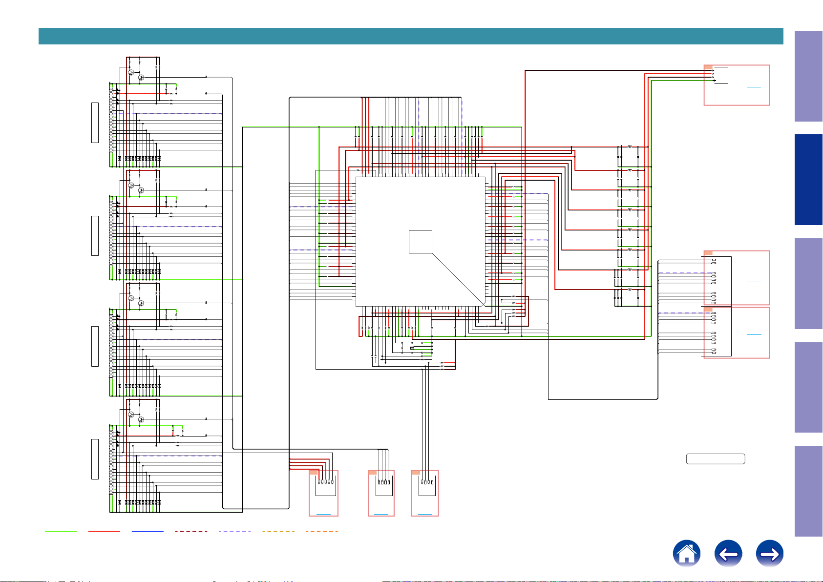
SCH12_HDMI SW2
1K
R2633
Q2604
KRC402E-RTK
19
HP_DET
18
+5V
17
GND
16
DDC_SDA
15
DDC_SCK
14
N.C.
13
CE_REMOTE
12
TXC-
11
TXC_SHLD
10
TXC+
9
TX0-
8
TX0_SHLD
7
TX0+
6
TX1-
5
TX1_SHLD
4
TX1+
3
TX2-
2
TX2_SHLD
1
TX2+
N2603
A0D7ABAR1990
HP_DET
DDC_SDA
DDC_SCK
CE_REMOTE
TXC_SHLD
TX0_SHLD
TX1_SHLD
TX2_SHLD
N2700
A0D7ABAR1990
HP_DET
DDC_SDA
DDC_SCK
CE_REMOTE
TXC_SHLD
TX0_SHLD
HDMI IN3
TX1_SHLD
TX2_SHLD
N2600
A0D7ABAR1990
HP_DET
DDC_SDA
DDC_SCK
CE_REMOTE
TXC_SHLD
TX0_SHLD
HDMI IN4 HDMI IN1HDMI IN2
TX1_SHLD
TX2_SHLD
N2601
A0D7ABAR1990
OPEN.
OPEN.
OPEN.
OPEN.
D2627
D2625
D2626
D2624
1K
R2689
Q2606
KRC402E-RTK
19
18
+5V
17
GND
16
15
14
N.C.
13
12
TXC-
11
10
TXC+
9
TX0-
8
7
TX0+
6
TX1-
5
4
TX1+
3
TX2-
2
1
TX2+
OPEN.
OPEN.
OPEN.
OPEN.
D2638
D2637
D2639
D2636
1K
R2610
Q2600
KRC402E-RTK
19
18
+5V
17
GND
16
15
14
N.C.
13
12
TXC-
11
10
TXC+
9
TX0-
8
7
TX0+
6
TX1-
5
4
TX1+
3
TX2-
2
1
TX2+
D2604 OPEN.
D2602 OPEN.
D2600 OPEN.
D2606 OPEN.
1K
R2611
Q2601
KRC402E-RTK
19
18
+5V
17
GND
16
15
14
N.C.
13
12
TXC-
11
10
TXC+
9
TX0-
8
7
TX0+
6
TX1-
5
4
TX1+
3
TX2-
2
1
TX2+
D2601 OPEN.
D2607 OPEN.
D2603 OPEN.
D2605 OPEN.
R2654
OPEN.
OPEN.
D2628
D2629
R2669
OPEN.
OPEN.
D2640
D2641
R2612
D2608 OPEN.
D2610 OPEN.
R2613
D2609 OPEN.
D2611 OPEN.
10K
Q2605
KRC402E-RTK
OPEN.
OPEN.
D2631
D2630
10K
Q2607
KRC402E-RTK
OPEN.
OPEN.
D2642
D2643
10K
Q2602
KRC402E-RTK
D2612 OPEN.
D2614 OPEN.
10K
Q2603
KRC402E-RTK
D2615 OPEN.
D2613 OPEN.
OPEN.
OPEN.
D2632
D2633
OPEN.
OPEN.
D2645
D2644
D2616 OPEN.
D2618 OPEN.
D2617 OPEN.
D2619 OPEN.
47K
47K
R2656
R2655
OPEN.
OPEN.
D2634
D2635
47K
47K
R2671
R2670
OPEN.
OPEN.
D2647
D2646
47K
47K
R2615
R2617
D2620 OPEN.
D2622 OPEN.
47K
47K
R2616
R2618
D2621 OPEN.
D2623 OPEN.
C2685
0.1
R2662
R2663
C2690
0.1
R2674
R2675
C2600
0.1
R2620
R2621
R2659
0
R2672
0
R2619
0
C2601
0.1
R2623
R2624
R2664
47K
0
0
R2673
47K
0
0
R2625
47K
0
0
R2622
0
R2639
47K
0
0
RX1_DDCDA
RX1_DDCCL
RX1_C-
RX1_C+
RX1_0-
RX1_0+
RX1_1-
RX1_1+
RX1_2-
RX1_2+
RX2_DDCDA
RX2_DDCCL
RX2_C-
RX2_C+
RX2_0-
RX2_0+
RX2_1-
RX2_1+
RX2_2-
RX2_2+
RX3_DDCDA
RX3_DDCCL
RX3_C-
RX3_C+
RX3_0-
RX3_0+
RX3_1-
RX3_1+
RX3_2-
RX3_2+
RX4_DDCDA
RX4_DDCCL
RX4_C-
RX4_C+
RX4_0-
RX4_0+
RX4_1-
RX4_1+
RX4_2-
RX4_2+
HPD1
RX1_5V
HPD2
RX2_5V
HPD3
RX3_5V
HPD4
RX4_5V
RX4_5V
RX1_DDCDA
RX1_DDCCL
RX2_DDCDA
RX2_DDCCL
RX3_CRX3_C+
RX3_0RX3_0+
RX3_1RX3_1+
RX3_2RX3_2+
RX4_CRX4_C+
RX4_0RX4_0+
RX4_1RX4_1+
RX4_2RX4_2+
RX3_DDCDA
RX3_DDCCL
RX4_DDCDA
RX4_DDCCL
RX1_5V
RX2_5V
RX3_5V
RX4_5V
0.1
C2604
C2615
0.1
C2616
0.1
0.1
C2605
0.1
C2606
0.1
C2607
0.1
C2608
0.1
C2609
0.1
C2612
G4
RX1_5V
RX4_5V
RX3_5V
RX2_5V
TO SW1
TO 8U-310223(13/19)
TO 4G
All Ref.No. has been described in the parts list are four digits.
But there are less than four digits of printed Ref.No. on the PCB, and they have become four digits after the header by adding "0" in the parts list.
4F
CEC5V
CEC3.3V
CEC1.1V2
DGND
TO
HDMI
SUPPLY
RX1_5V
RX2_5V
RX3_5V
10/6.3
10/6.3
2125
2125
C2632
C2602
R2601
10
73
74
75
RX3SCL
76
RX2SDA
77
RX2SCL
78
VDD11
79
AVDD33RX1
80
P1RXCM
81
P1RXCP
82
AVDD11RX1
83
P1RX0M
84
P1RX0P
85
AVDD11RX1
86
P1RX1M
87
P1RX1P
88
AVDD11RX1
89
P1RX2M
90
P1RX2P
91
VSS
92
AVDD33RX0
93
P0RXCM
94
P0RXCP
95
AVDD11RX0
96
P0RX0M
97
P0RX0P
98
AVDD11RX0
99
P0RX1M
100
P0RX1P
101
AVDD11RX0
102
P0RX2M
103
P0RX2P
104
VSS
105
107:
RX1SDA
106
108:
RX1SCL
107
108
TX1ARCIN
CEC
109
110
10K
47K
47K
R2606
R2607
R2602
CEC_COM
RX2_1-
RX2_1+
RX2_2-
RX2_2+
0.1
0.1
0.1
C2628
C2620
C2618
60
61
63
64
66
67
VSS
VDD1168NIRQ169VDD33
P2RX1M62P2RX1P
P2RX2M65P2RX2P
AVDD11RX2
RX0P5V
RX3SDA
HDMI SW2
Slave Address:70
70
RX3P5V71RX2P5V72RX1P5V
0.1
C2619
73:
74:
MN864788
RX0SDA
RX0SCL
TX0ARCIN
VDD11
NTEST
HSCL0
NRESET
HSDA0
VDD33
SYSCLK/XI
NC/XO
112
113
114
115
116
117
47
47
0.1
0.1
R2630
C2610
R2631
C2625
OPEN
OPEN
C2647
C2648
HPD4
HPD3
HPD2
HPD1
4C
HPD1
HPD2
HPD3
HPD4
TO
EXPANDER
TO 8U-310223(3/19)
TO C4
VSS
118
119
120
121
0.1
C2627
1M
R2628
111
RX1_2-
RX1_2+
RX2_C-
RX2_C+
RX2_0-
RX2_0+
0.1
0.1
C2630
C2631
51
53
54
55
57
58
VSS
P2RXCM56P2RXCP
P2RX0M59P2RX0P
AVDD33RX2
AVDD11RX2
AVDD11RX2
VSS
145
U2601
VDD11
VDD11
SCLK/LPSA1
MOSI/LPSA0
MISO
CH0AMCLK
VSS
VSS
NCS
122
123
124
125
126
127
128
129
130
47K
10K
0.1
0.1
C2633
R2604
R2605
C2636
C2614
10P
1 3
27MHz
X2601
C2613
12P
C2622 1000P
1K
R2632
0C
HSCL
HSDA
SW2_HINT
TO CPU
TO 8U-310223(2/19)
TO C0
RX1_1+
0.1
C2621
50
P3RX2M52P3RX2P
AVDD11RX3
VDD33IO
CH0ABCLK
131
132
R2608
R2609
R2614
SW2_RST
RX1_1-
48
P3RX1M49P3RX1P
CH0ALRCLK
CH0ASD3
133
10K
10K
10K
RX1_0+
0.1
C2623
47
AVDD11RX3
CH0ASD2
CH0ASD1
134
135
RX1_0-
0.1
C2624
44
45
P3RX0M46P3RX0P
AVDD11RX3
36:
35:
2:
TX0HPD
1:
TX0SDA
CH0ASD0
VDD11
136
137
0.1
C2629
RX1_C+
NIRQA1
VDD11
VDD33
138
RX1_C-
42
P3RXCM43P3RXCP
(NC)
139
0.1
C2626
40
41
VSS
AVDD33RX3
TX1SCL
VSS
140
141
0.1
0.1
C2634
C2637
38
39
VDD33
PVDD33
P0TXCM
AVDD11TX
P0TXCP
P0TX0M
AVDD33TX
P0TX0P
P0TX1M
AVDD11TX
P0TX1P
P0TX2M
AVDD11TX
P0TX2P
P1TXCM
AVDD11TX
P1TXCP
P1TX0M
AVDD33TX
P1TX0P
P1TX1M
AVDD11TX
P1TX1P
P1TX2M
AVDD11TX
P1TX2P
CH1ABCLK
CH1ALRCLK
CH1ASD0
TX1SDA
TX1HPD
142
143
10/6.3
10/6.3
2125
2125
C2617
C2603
37
NIRQA0
VSS
VDD11
VSS
VDD11
VSS
TX0SCL
144
R2634
L2602
SW2AVDD11RX
SW2AVDD33RX
36
0.1
C2658
35
34
33
C2665
32
31
30
C2640
29
28
27
C2611
26
25
24
C2642
23
22
C2641
21
20
19
C2688
18
17
16
C2643
15
14
13
C2689
12
11
10
C2691
9
8
C2652
7
6
5
4
3
R2635
2
1
R2637
R2638
R2641
R2640
10K
0.1
0.1
0.1
0.1
0.1
0.1
0.1
0.1
0.1
0.1
10K
1.8K
1.8K
1.8K
1.8K
P0_D0-
P0_D0+
P0_D1-
P0_D1+
P0_D2-
P0_D2+
P1_D0-
P1_D0+
P1_D1-
P1_D1+
P1_D2-
P1_D2+
P0_DDCDA
P0_DDCCL
P1_DDCDA
P1_DDCCL
P0_C-
P0_C+
P1_C-
P1_C+
SW2PVDD33
SW2VDD33
SW2VDD11
SW2VDD33IO
SW2AVDD11Tx
SW2AVDD33Tx
FBMJ3216HL160NT
OPEN
4.7u
C2681
C2674
FBMJ3216HL160NT
L2605
OPEN
4.7u
C2678
C2672
BLM21PG221
OPEN
4.7u
C2660
C2679
BLM21PG221
OPEN
4.7u
C2676
C2645
BLM21PG221
4.7u
OPEN
C2673
C2667
BLM21PG221
OPEN
4.7u
C2669
C2686
BLM21PG221
4.7u
OPEN
OPEN.C2663
C2682
C2675
BLM21PG221
OPEN
OPEN.C2656
4.7u
C2671
C2677
L2606
L2600
L2601
L2607
L2603
L2604
OPEN.
C2644
OPEN.
C2646
4.7u
C2670
4.7u
C2651
4.7u
C2680
4.7u
P1_DDCDA
P1_DDCCL
C2687
P1_CP1_C+
4.7u
P1_D0P1_D0+
C2684
P1_D1P1_D1+
4.7u
P1_D2P1_D2+
C2657
P0_CP0_C+
P0_D0P0_D0+
P0_D1P0_D1+
P0_D2P0_D2+
P0_DDCCL
P0_DDCDA
8U-310223(12/19)
DIGITAL_UNIT
HDMI SW2
TO 8U-310223(10/19)
G2
P1_DDCDA
P1_DDCCL
P1_CP1_C+
P1_D0P1_D0+
P1_D1P1_D1+
P1_D2P1_D2+
G3
P0_CP0_C+
P0_D0P0_D0+
P0_D1P0_D1+
P0_D2P0_D2+
P0_DDCCL
P0_DDCDA
Condential
TO F4
TO 2G
TO HDMI SW1
TO 3G
TO 8U-310223(17/19) TO 8U-310223(13/19)
TO HDMI TX
Caution in
servicing
Electrical Mechanical Repair Information Updating
GND LINE
POWER+ LINE
POWER- LINE
AUDIO SIGNAL
TMDS SIGNAL
ANALOG VIDEO
DIGITAL VIDEO
21
Page 22
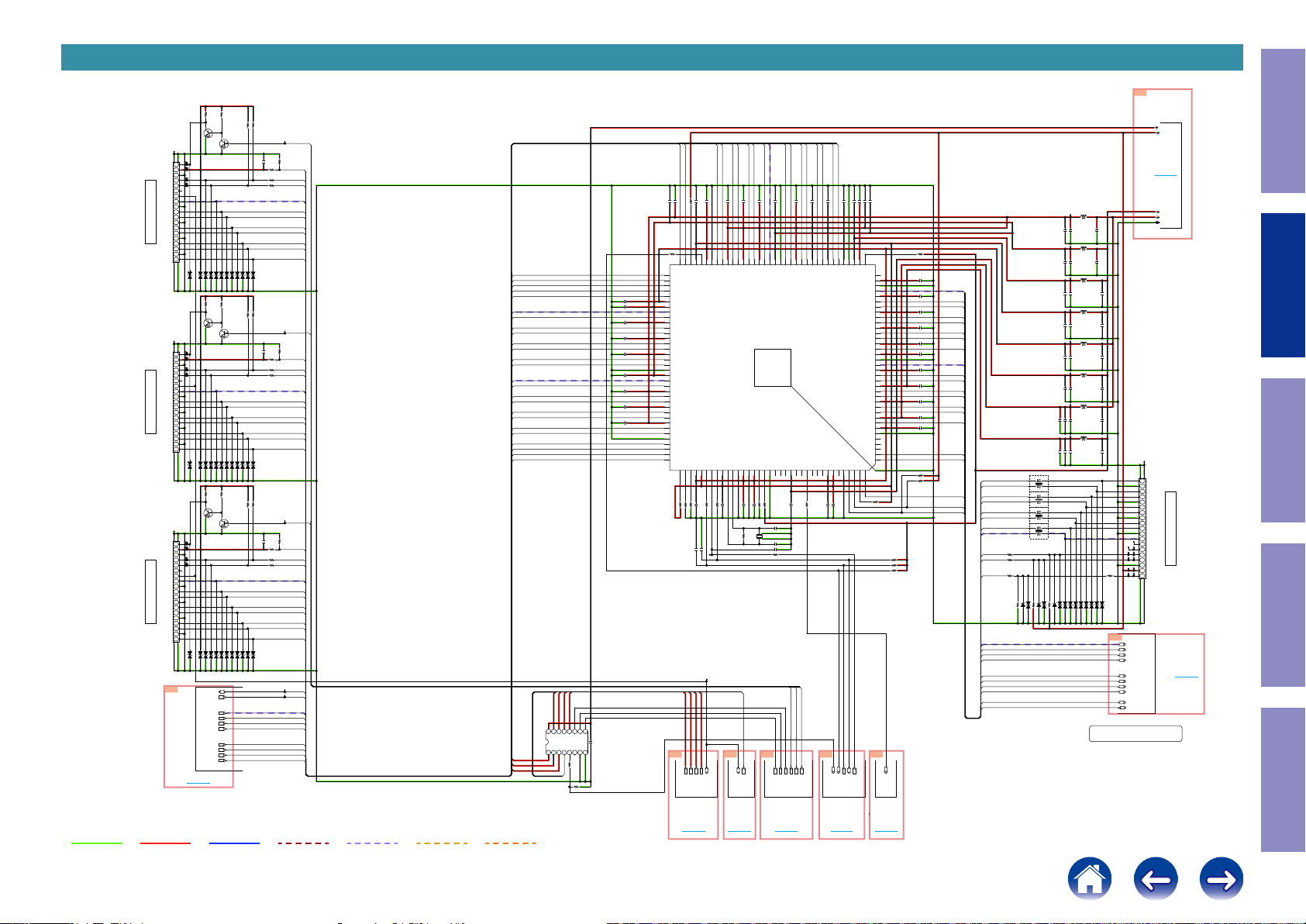
SCH13_HDMI SW1
1K
R2400
Q2400
KRC402E-RTK
19
HP_DET
18
+5V
17
GND
16
DDC_SDA
15
DDC_SCK
14
N.C.
13
CE_REMOTE
12
TXC-
11
TXC_SHLD
10
TXC+
9
TX0-
8
TX0_SHLD
7
TX0+
6
TX1-
5
TX1_SHLD
4
TX1+
3
TX2-
2
TX2_SHLD
1
TX2+
N2400
GND LINE
A0D7ABAR1990
CE_REMOTE
HDMI IN6 HDMI IN5
A0D7ABAR1990
CE_REMOTE
HDMI IN7
A0D7ABAR1990
POWER+ LINE
19
HP_DET
18
+5V
17
GND
16
DDC_SDA
15
DDC_SCK
14
N.C.
13
12
TXC-
11
TXC_SHLD
10
TXC+
9
TX0-
8
TX0_SHLD
7
TX0+
6
TX1-
5
TX1_SHLD
4
TX1+
3
TX2-
2
TX2_SHLD
1
TX2+
N2401
19
HP_DET
18
+5V
17
GND
16
DDC_SDA
15
DDC_SCK
14
N.C.
13
12
TXC-
11
TXC_SHLD
10
TXC+
9
TX0-
8
TX0_SHLD
7
TX0+
6
TX1-
5
TX1_SHLD
4
TX1+
3
TX2-
2
TX2_SHLD
1
TX2+
N2402
2G
from HDMI SW2
TO G2
D2408 OPEN.
D2412 OPEN.
D2400 OPEN.
D2404 OPEN.
1K
R2401
Q2401
KRC402E-RTK
D2409 OPEN.
D2413 OPEN.
D2401 OPEN.
D2405 OPEN.
R2402
Q2402
KRC402E-RTK
D2410 OPEN.
D2406 OPEN.
D2402 OPEN.
D2414 OPEN.
P1_DDCDA
P1_DDCCL
P1_C-
P1_C+
P1_D0P1_D0+
P1_D1-
TO 8U-310223(12/19)
P1_D1+
P1_D2P1_D2+
POWER- LINE
1K
R2404
D2416 OPEN.
D2420 OPEN.
R2405
D2417 OPEN.
D2421 OPEN.
R2406
D2418 OPEN.
D2422 OPEN.
10K
Q2404
KRC402E-RTK
D2424 OPEN.
D2428 OPEN.
10K
Q2405
KRC402E-RTK
D2425 OPEN.
D2429 OPEN.
10K
Q2406
KRC402E-RTK
D2426 OPEN.
D2430 OPEN.
D2432 OPEN.
D2436 OPEN.
D2433 OPEN.
D2437 OPEN.
D2434 OPEN.
D2438 OPEN.
47K
47K
R2408
R2412
D2440 OPEN.
D2444 OPEN.
47K
47K
R2413
R2409
D2441 OPEN.
D2445 OPEN.
47K
47K
R2414
R2410
D2442 OPEN.
D2446 OPEN.
C2400
R2436
47K
0.1
0
R2424
R2425
0
R2426
0
C2401
R2437
47K
0.1
0
R2427
R2428
0
R2429
0
C2402
R2438
47K
0.1
0
R2430
R2431
0
R2432
0
AUDIO SIGNAL
RX5_5V
RX5_DDCDA
RX5_DDCCL
RX6_5V
RX6_DDCDA
RX6_DDCCL
RX7_DDCDA
RX7_DDCCL
P1_DDCDA
P1_DDCCL
P1_D0P1_D0+
P1_D1P1_D1+
P1_D2P1_D2+
HPD5
RX5_C-
RX5_C+
RX5_0-
RX5_0+
RX5_1-
RX5_1+
RX5_2-
RX5_2+
HPD6
RX6_C-
RX6_C+
RX6_0-
RX6_0+
RX6_1-
RX6_1+
RX6_2-
RX6_2+
HPD7
RX7_5V
RX7_C-
RX7_C+
RX7_0-
RX7_0+
RX7_1-
RX7_1+
RX7_2-
RX7_2+
P1_CP1_C+
TMDS SIGNAL
ANALOG VIDEO
RX7_5V
P1_DDCDA
P1_DDCCL
RX5_DDCDA
RX5_DDCCL
RX6_CRX6_C+
RX6_0RX6_0+
RX6_1RX6_1+
RX6_2RX6_2+
RX7_CRX7_C+
RX7_0RX7_0+
RX7_1RX7_1+
RX7_2RX7_2+
RX6_DDCDA
RX6_DDCCL
RX7_DDCDA
RX7_DDCCL
RX5_5V
RX6_5V
RX7_5V
DIGITAL VIDEO
All Ref.No. has been described in the parts list are four digits.
But there are less than four digits of printed Ref.No. on the PCB, and they have become four digits after the header by adding "0" in the parts list.
3F
TO HDMI
SUPPLY
TO 8U-310223(10/19)
CEC_STBY5V
CEC5V
P1_C-
P1_D2-
0.1
C2426
51
P3RX2M52P3RX2P
VSS
145
VDD33IO
130
0.1
C2414
HPD6
HPD7
HPD7
HINSELA
P1_D1-
P1_D1+
48
50
P3RX1M49P3RX1P
AVDD11RX3
CH0ABCLK
CH0ALRCLK
CH0ASD3
131
132
133
33
R2444
HPD5
HPD6
HPD5
P1_D0-
P1_D0+
0.1
0.1
C2428
C2429
44
45
46
47
P3RX0M
P3RX0P
AVDD11RX3
AVDD11RX3
36:
35:
2:
TX0HPD
1:
TX0SDA
CH0ASD2
CH0ASD1
CH0ASD0
VDD11
134
135
136
137
0.1
C2415
9B
TO 8U-310223(2/19)
TO B9
P1_C+
0.1
C2430
40
41
42
VSS
P3RXCM43P3RXCP
AVDD33RX3
NIRQA1
VDD11
VSS
VDD33
(NC)
TX1SCL
138
139
140
141
0.1
C2416
HSCL
HSDA
H5VDET
SW1_HINT
TO CPU
0.1
0.1
10/6.3
10/6.3
2125
2125
C2496
C2499
C2438
C2484
39
37
38
VDD33
NIRQA0
PVDD33
VSS
P0TXCM
AVDD11TX
P0TXCP
P0TX0M
AVDD33TX
P0TX0P
P0TX1M
AVDD11TX
P0TX1P
P0TX2M
AVDD11TX
P0TX2P
VDD11
VSS
P1TXCM
AVDD11TX
P1TXCP
P1TX0M
AVDD33TX
P1TX0P
P1TX1M
AVDD11TX
P1TX1P
P1TX2M
AVDD11TX
P1TX2P
VDD11
VSS
CH1ABCLK
CH1ALRCLK
CH1ASD0
TX1SDA
TX1HPD
TX0SCL
142
143
144
R2421
1E
SW1_RST
TO DIR/
DA POWER
TO 8U-310223(5/19)
36
35
34
33
32
31
30
29
28
27
26
25
24
23
22
21
20
19
18
17
16
15
14
13
12
11
10
9
8
7
6
5
4
3
2
1
10K
R2456
R2457
R2458
TO E1
OPEN
OPEN
10K
Z2_SPDIF
R2440
C2497
C2498
C2434
C2418
C2421
C2435
C2422
C2436
C2423
C2433
C2437
R2476
R2477
OPEN
0.1
0.1
0.1
0.1
0.1
0.1
0.1
0.1
0.1
0.1
0.1
1.8K
1.8K
P3_D2+
P3_D2P3_D1+
P3_D1P3_D0+
P3_D0-
P2_D0-
P2_D0+
P2_D1-
P2_D1+
P2_D2-
P2_D2+
P3_HPD
P3_DDCDA
P3_DDCCL
P2_DDCDA
P2_DDCCL
P3_C-
P3_C+
P2_C-
P2_C+
P3_D2+
P3_D2-
P3_D1+
P3_D1-
P3_D0+
P3_D0-
P3_C+
P3_C-
P3_DDCCL
P3_DDCDA
P3_HPD
P2_CP2_C+
P2_D0P2_D0+
P2_D1P2_D1+
P2_D2P2_D2+
P2_DDCCL
P2_DDCDA
L2402
3
1
3
1
3
1
3
1
1.8K
R2422
D2450 OPEN.
R2423
0x2
4
2
R2403
0x2
4
2
R2433
0x2
4
2
R2407
EXC24CH900U
4
2
1.8K
OPEN
R2434
D2411 OPEN.
D2407
OPEN
C2470
OPEN
C2467
OPEN
D2415 OPEN.
D2403
OPEN
C2469
OPEN
C2466
OPEN
C2455
OPEN
C2439
OPEN
C2462
OPEN
C2448
4.7u
C2477
4.7u
C2473
D2423 OPEN.
FBMJ3216HL160NT
4.7u
C2476
FBMJ3216HL160NT
L2404
4.7u
C2472
BLM21PG221
4.7u
C2474
BLM21PG221
4.7u
C2471
BLM21PG221
4.7u
C2468
BLM21PG221
4.7u
C2479
BLM21PG221
BLM21PG221
OPEN.C2410 OPEN.C2451
D2427 OPEN.
D2435 OPEN.
D2431 OPEN.
SW1AVDD11RX
SW1AVDD33RX
SW1PVDD33
SW1VDD33
SW1VDD11
SW1VDD33IO
SW1AVDD11Tx
SW1AVDD33Tx
R2411
0
0
R2415
R2494
0
UDZS5.1B
10K
D2419
R2435
8U-310223(13/19)
DIGITAL_UNIT
HDMI SW1
OPEN.C2475
OPEN.C2452
L2406
4.7u
C2465
L2400
4.7u
C2446
L2401
4.7u
C2403
L2407
4.7u
C2480
L2403
4.7u
C2478
L2405
4.7u
C2459
R2439
0
D2443 OPEN.
D2449 OPEN.
D2439 OPEN.
D2447 OPEN.
G5
P2_CP2_C+
P2_D0P2_D0+
P2_D1P2_D1+
P2_D2P2_D2+
P2_DDCCL
P2_DDCDA
Condential
TO F3
CEC3.3V
CEC1.1V1
DGND
N5010
A0D7ABAR1990
TX2+
1
TX2_SHLD
2
TX2-
3
TX1+
4
TX1_SHLD
5
TX1-
6
TX0+
7
TX0_SHLD
8
TX0-
9
TXC+
10
TXC_SHLD
11
TXC-
12
CE_REMOTE
13
N.C.
14
DDC_SCK
15
DDC_SDA
16
GND
17
+5V
18
HP_DET
19
TO HDMI TX
HDMI Z2out
TO 5G
TO 8U-310223(17/19)
RX4_5V
16
VCC
U2400
1B42B33B24B15A6NC7OE8
SN74CBT3251PWR
RX3_5V
RX2_5V
RXF_5V
RX1_5V
R2448
R2449
8.2K
2.2K
RX6_5V
RX5_5V
10/6.3
10/6.3
2125
2125
C2492
C2493
R2441
10
73
74
75
RX3SCL
76
RX2SDA
77
RX2SCL
0.1
C2411
C2431
C2432
C2454
C2461
C2481
C2482
C2483
C2485
9
S210S111S012B813B714B615B5
0.1
GND
C2404
78
VDD11
0.1
79
AVDD33RX1
80
P1RXCM
81
P1RXCP
0.1
82
AVDD11RX1
83
P1RX0M
84
P1RX0P
0.1
85
AVDD11RX1
86
P1RX1M
87
P1RX1P
0.1
88
AVDD11RX1
89
P1RX2M
90
P1RX2P
91
VSS
0.1
92
AVDD33RX0
93
P0RXCM
94
P0RXCP
0.1
95
AVDD11RX0
96
P0RX0M
97
P0RX0P
0.1
98
AVDD11RX0
99
P0RX1M
100
P0RX1P
0.1
101
AVDD11RX0
102
P0RX2M
103
P0RX2P
104
VSS
105
RX1SDA
106
RX1SCL
107
108
CEC
109
110
10K
47K
R2420
R2419
RX4_5V
4G
TO SW2
TO 8U-310223(12/19)
TO G4
RX5_1+
RX5_2-
RX5_2+
0.1
0.1
0.1
47K
R2416
C2417
C2409
C2427
63
64
66
67
70
VSS
VDD1168NIRQ169VDD33
P2RX2M65P2RX2P
RX3P5V71RX2P5V72RX1P5V
AVDD11RX2
73:
RX0P5V
74:
RX3SDA
HDMI SW1
Slave Address:40
MN864788
107:
RX0SDA
108:
RX0SCL
TX1ARCIN
TX0ARCIN
VDD11
NTEST
HSCL0
NRESET
HSDA0
VDD33
SYSCLK/XI
NC/XO
111
112
113
114
115
116
117
118
119
47
47K
0.1
0.1
C2405
C2406
R246047R2461
R2447
OPEN
OPEN
C2458
C2457
RX2_5V
RX3_5V
RX1_5V
G6
RX3_5V
RX2_5V
RX1_5V
RX4_5V
CEC_COM
TO HDMI
TX
TO 8U-310223(17/19)
TO 6G
P1_D2+
RX5_C-
RX5_C+
RX5_0-
RX5_0+
RX5_1-
0.1
0.1
0.1
C2424
C2420
C2425
53
54
55
57
58
60
61
VSS
P2RXCM56P2RXCP
P2RX0M59P2RX0P
P2RX1M62P2RX1P
AVDD33RX2
AVDD11RX2
AVDD11RX2
U2401
VSS
VSS
VSS
NCS
VDD11
VDD11
SCLK/LPSA1
MOSI/LPSA0
MISO
0.1
C2407
1M
RXF_5V
CEC_COM
121
RXF_5V
122
X2400
123
124
47K
10K
0.1
C2408
R2418
R2446
C2413
1 3
27MHz
C2412
C2419 1000P
R2462
5C
125
CH0AMCLK
126
127
128
129
10P
12P
1K
HINSELB
HINSELC
TO
EXPANDER
TO 8U-310223(3/19)
TO C5
120
R2455
Caution in
servicing
Electrical Mechanical Repair Information Updating
22
Page 23
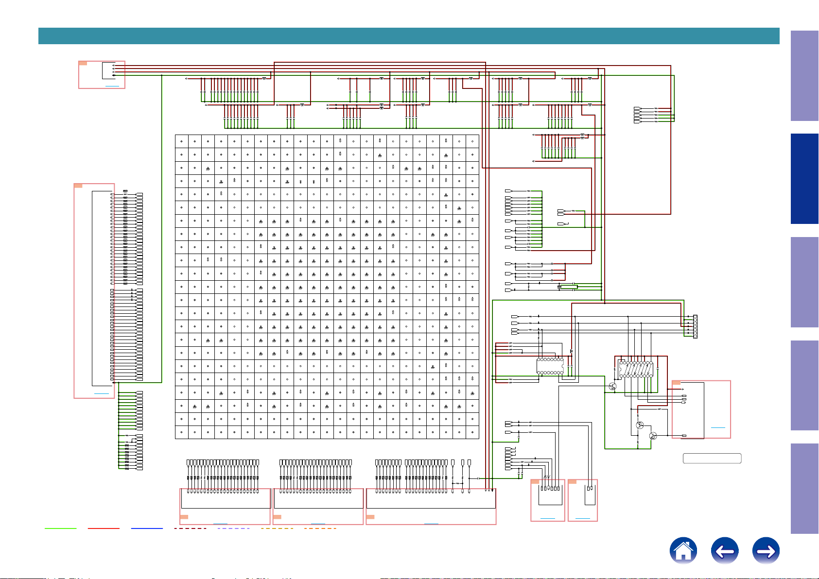
SCH14_IP OSD
6F
DV5V
DV3.3V
DV1.8V
DGND
TO HDMI
SUPPLY
TO 8U-310223(10/19)
TO F6
G7
8KOPI_PCK
8KOPI_HSYNC
8KOPI_VSYNC
8KOPI_DE
8KOPI_Y11/R7
8KOPI_Y10/R6
8KOPI_Y9/R5
8KOPI_Y8/R4
8KOPI_Y7/R3
8KOPI_Y6/R2
8KOPI_Y5/R1
8KOPI_Y4/R0
8KOPI_Y3/G7
8KOPI_Y2/G6
8KOPI_Y1/G5
TO 8U-310223(16/19)
8KOPI_Y0/G4
8KOPI_C11/G3
8KOPI_C10/G2
8KOPI_C9/G1
8KOPI_C8/G0
8KOPI_C7/B7
8KOPI_C6/B6
8KOPI_C5/B5
8KOPI_C4/B4
8KOPI_C3/B3
8KOPI_C2/B2
8KOPI_C1/B1
8KOPI_C0/B0
PO8KI_PCK
PO8KI_HSYNC
TO VIDEO PLD
PO8KI_VSYNC
PO8KI_DE
PO8KI_Y11/R7
PO8KI_Y10/R6
PO8KI_Y9/R5
PO8KI_Y8/R4
PO8KI_Y7/R3
PO8KI_Y6/R2
PO8KI_Y5/R1
PO8KI_Y4/R0
PO8KI_Y3/G7
PO8KI_Y2/G6
PO8KI_Y1/G5
PO8KI_Y0/G4
PO8KI_C11/G3
PO8KI_C10/G2
PO8KI_C9/G1
PO8KI_C8/G0
PO8KI_C7/B7
PO8KI_C6/B6
PO8KI_C5/B5
PO8KI_C4/B4
PO8KI_C3/B3
PO8KI_C2/B2
PO8KI_C1/B1
PO8KI_C0/B0
DGND
TO 7G
GND LINE
POWER+ LINE
R2804
R2884
R2809
R2804
R2804
R2804
R2805
R2805
R2805
R2805
R2808
R2806
R2806
R2808
R2806
R2806
R2808
R2808
R2807
R2807
R2809
R2809
R2807
R2807
R2810
R2809
R2810
R2810
R2810
R2900
R2914
R2899
R2899
R2899
R2898
R2899
R2898
R2898
R2898
7 8
7 8
5 6
3 4
1 2
7 8
5 6
3 4
1 2
1 2
7 8
5 6
3 4
3 4
1 2
5 6
7 8
7 8
5 6
1 2
3 4
3 4
1 2
7 8
5 6
1 2
3 4
5 6
5 6
3 4
7 8
1 2
1 2
3 4
7 8
5 6
10x4
47
.8KOPI_PCK
A3
10x4
.8KOPI_HSYNC
J3
10x4
.8KOPI_VSYNC
B3
10x4
.8KOPI_DE
A2
10x4
.8KOPI_Y11/R7
A1
10x4
.8KOPI_Y10/R6
B2
10x4
.8KOPI_Y9/R5
B1
10x4
.8KOPI_Y8/R4
C2
10x4
.8KOPI_Y7/R3
C1
10x4
.8KOPI_Y6/R2
D3
10x4
.8KOPI_Y5/R1
D2
10x4
.8KOPI_Y4/R0
D1
10x4
.8KOPI_Y3/G7
E3
10x4
.8KOPI_Y2/G6
E2
10x4
.8KOPI_Y1/G5
E1
10x4
.8KOPI_Y0/G4
F4
10x4
.8KOPI_C11/G3
F3
10x4
.8KOPI_C10/G2
F2
10x4
.8KOPI_C9/G1
F1
10x4
.8KOPI_C8/G0
G4
10x4
.8KOPI_C7/B7
G3
10x4
.8KOPI_C6/B6
G2
10x4
.8KOPI_C5/B5
G1
10x4
.8KOPI_C4/B4
H4
10x4
.8KOPI_C3/B3
H3
10x4
.8KOPI_C2/B2
H2
10x4
.8KOPI_C1/B1
H1
10x4
.8KOPI_C0/B0
J4
PO8KI_PCK
K2
PO8KI_HSYNC
J2
PO8KI_VSYNC
K1
PO8KI_DE
J1
PO8KI_Y11/R7
P4
PO8KI_Y10/R6
P3
PO8KI_Y9/R5
P2
PO8KI_Y8/R4
P1
PO8KI_Y7/R3
R4
PO8KI_Y6/R2
R3
PO8KI_Y5/R1
R2
PO8KI_Y4/R0
R1
PO8KI_Y3/G7
T2
PO8KI_Y2/G6
T1
PO8KI_Y1/G5
U4
PO8KI_Y0/G4
U3
PO8KI_C11/G3
U2
PO8KI_C10/G2
U1
PO8KI_C9/G1
V4
PO8KI_C8/G0
V3
PO8KI_C7/B7
V2
PO8KI_C6/B6
V1
PO8KI_C5/B5
W4
PO8KI_C4/B4
W3
PO8KI_C3/B3
W2
PO8KI_C2/B2
W1
PO8KI_C1/B1
Y2
PO8KI_C0/B0
Y1
N1
N2
N3
N4
M1
M2
M3
M4
L1
L2
L3
L4
4.7K
TX256fs/DSDMCK
D6
TX64fs/DSDSCK
C5
4.7K
TX64fs/DSDSCK
C6
4.7Kx4
TXSPDIF/DSD0
B4
4.7Kx4
TXI2S0/DSD1
A4
4.7Kx4
TXI2S1/DSD2
A5
4.7Kx4
TXI2S2/DSD3
B5
4.7Kx4
TXI2S3/DSD4
C4
4.7Kx4
TXfs/DSD5
A6
4.7Kx4
TX_ARC2OUT
A7
4.7Kx4
TX_ARC1OUT
B7
POWER- LINE
DVDD_TX
4.7u
0.1
0.1
0.1
0.1
0.1
0.1
0.1
C2807
C2813
C2809
C2808
C2811
C2810
C2806
C2805
DDR_1.8V
0.1
4.7u
C2814
A3
2
OSD_CLK/EXT_CLK
.8KOPI_PCK
B3
25
OSD_VS
.8KOPI_VSYNC
C3
48
GND
DGND
D3
71
OSD_IN18/EXT_DIN2
.8KOPI_Y6/R2
94
E3
OSD_IN15/VBI_CS
.8KOPI_Y3/G7
117
F3
OSD_IN11/P47
.8KOPI_C11/G3.8KOPI_C10/G2
140
G3
OSD_IN7/P43
163
H3
OSD_IN3/P39
.8KOPI_C3/B3
186
J3
SFL
.8KOPI_HSYNC
209
K3
DVDD_IO
DVDDIO_TX
232
L3
P34
DGND
255
M3
P30
DGND
278
N3
P26
DGND
301
P3
P22
PO8KI_Y10/R6
324
R3
P18
347
T3
GND
DGND
370
U3
P12
PO8KI_Y0/G4
393
V3
PO8KI_C8/G0
416
W3
PO8KI_C4/B4
Y3
439
DDR_DQS2
TX_DDRDQS2
AA3
462
GND
DGND
AB3
485
DDR_DQ17
TX_DDRDQ17
AC3
508
DDR_DQ22
TX_DDRDQ22
TX_DDRDM0
TX_DDRQSB1
TX_DDRDM1
TX_DDRDQS1
AA20
AC18
AA19
AB17
47x4
47
5 6
R282247R2823
R2824
DR_TXDM0
DR_TXDM1
DR_TXDQS1
DR_TXDQSB1
C2812
A4
3
AUD_IN1
TXI2S0/DSD1
B4
26
AUD_IN0
TXSPDIF/DSD0
C4
49
AUD_IN4
TXI2S3/DSD4
D4
72
GND
DGND
95
E4
DVDD_IO
DVDDIO_TX
118
119
F4
OSD_IN12
.8KOPI_Y0/G4
141
142
G4
OSD_IN8/P44
.8KOPI_C8/G0.8KOPI_C7/B7.8KOPI_C6/B6
164
165
H4
OSD_IN4/P40
.8KOPI_C4/B4
187
188
J4
OSD_IN0/P36
.8KOPI_C0/B0
210
211
K4
DVDD_IO
DVDDIO_TX
233
234
L4
P35
DGND
256
257
M4
P31
DGND
279
280
N4
P27
DGND
302
303
P4
P23
PO8KI_Y11/R7
325
326
R4
P19
PO8KI_Y7/R3
348
349
T4
GND
DGND
371
372
U4
P13
PO8KI_Y1/G5
394
395
V4
P8
P9
PO8KI_C9/G1
417
418
W4
P4
P5
PO8KI_C5/B5
Y4
440
441
GND
DGND
AA4
463
464
DDR_DQSB2
TX_DDRQSB2
AB4
486
487
DDR_DM2
TX_DDRDM2
AC4
509
510
DDR_DQ25
TX_DDRDQ1
TX_DDRDQ3
TX_DDRDQ4
TX_DDRDQ2
TX_DDRDQ0
AC23
AA23
AB23
AC21
AB20
47x4
47x4
47x4
47x4
47x4
47x4
3 4
1 2
7 8
7 8
3 4
5 6
R2825
R2826
R2821
R2826
R2825
R2826
DR_TXDQ0
DR_TXDQ1
DR_TXDQ3
DR_TXDQ2
DR_TXDQ4
TO 8G
TMDS SIGNAL
4
27
50
73
96
TX_DDRDQ5
AB21
47x4
1 2
R2826
DR_TXDQ5
1
2 3 4 5 6 7 8
A2
A1
1
OSD_DE
OSD_IN23/EXT_DIN7
A
.8KOPI_Y11/R7
.8KOPI_DE
B1
B2
24
OSD_IN21/EXT_DIN5
OSD_IN22/EXT_DIN6
B
.8KOPI_Y9/R5
.8KOPI_Y10/R6
C1
C2
47
OSD_IN19/EXT_DIN3
OSD_IN20/EXT_DIN4
C
.8KOPI_Y7/R3
.8KOPI_Y8/R4
D1
D2
70
OSD_IN16/EXT_DIN0
OSD_IN17/EXT_DIN1
D
.8KOPI_Y5/R1
.8KOPI_Y4/R0
93
E1
E2
OSD_IN13/VBI_SCK
OSD_IN14/VBI_MOSI
E
.8KOPI_Y1/G5
.8KOPI_Y2/G6
116
F1
F2
OSD_IN9/P45
OSD_IN10/P46
F
.8KOPI_C9/G1
139
G1
G2
OSD_IN5/P41
OSD_IN6/P42
G
.8KOPI_C5/B5
162
H1
H2
OSD_IN1/P37
OSD_IN2/P38
H
.8KOPI_C2/B2
.8KOPI_C1/B1
185
J1
J2
DE
HS
J
PO8KI_DE
PO8KI_HSYNC
208
K1
K2
VS
PCLK
K
PO8KI_VSYNC
PO8KI_PCK
231
L1
L2
P32
P33
L
DGND
DGND
254
M1
M2
P28
P29
M
DGND
DGND
277
N1
N2
P24
P25
N
DGND
DGND
300
P1
P2
P20
P21
P
PO8KI_Y8/R4
PO8KI_Y9/R5
323
R1
R2
P16
P17
R
PO8KI_Y5/R1
PO8KI_Y4/R0 PO8KI_Y6/R2
346
T1
T2
P14
P15
T
PO8KI_Y3/G7
PO8KI_Y2/G6
369
U1
U2
P10
P11
U
PO8KI_C10/G2
PO8KI_C11/G3
392
V1
V2
P6
P7
V
PO8KI_C6/B6
PO8KI_C7/B7
415
W1
W2
P2
P3
W
PO8KI_C2/B2
PO8KI_C3/B3
Y1
Y2
438
P0
P1
Y
PO8KI_C0/B0
PO8KI_C1/B1
AA1
AA2
461
DDR_DQ18
GND
AA
TX_DDRDQ18
DGND
AB1
AB2
484
DDR_DQ21
DDR_DQ19
AB
TX_DDRDQ21
TX_DDRDQ19
AC1
AC2
507
DDR_DQ16
DDR_DQ20
AC
TX_DDRDQ16 TX_DDRDQ28
TX_DDRDQ20
TX_DDRQSB0
TX_DDRDQS0
AC22
AB22
47x4
47x4
47x4
7 8
5 6
3 4
R2824
R2821
R2821
DR_TXDQS0
DR_TXDQSB0
G8
AUDIO SIGNAL
L2801
BLM21PG221
0.01
0.1
0.1
0.1
0.01
0.01
0.01
0.1
0.1
C2825
C2817
C2823
C2815
C2827
C2831
C2829
C2819
C2821
0.01
0.1
0.1
0.01
0.1
0.1
0.1
0.01
0.01
C2828
C2816
C2824
C2830
C2818
C2822
C2820
C2826
C2832
A5
A6
A7
A8
6
7
5
AUD_IN2
AUD_IN5
ARC2_OUT
MOSI1
TX_ARC2OUT
TXfs/DSD5
TXI2S1/DSD2
B5
28
AUD_IN3
TXI2S2/DSD3
C5
51
DSD_CLK
TX64fs/DSDSCK TX64fs/DSDSCK
D5
74
DVDD_IO
DVDDIO_TX
Y5
442
DDR_DQ23
TX_DDRDQ23
AA5
465
DDR_DQ26
TX_DDRDQ26
AB5
488
DDR_DQ30
TX_DDRDQ30 TX_DDRDQ31
AC5
511
DDR_DQ28
TX_DDRDQ7
TX_DDRDQ6
TX_DDRDQ8
TX_DDRDQ9
Y21
Y17
AC20
AB18
47x4
47x4
47x4
5 6
5 6
1 2
R2825
R2824
R2827
DR_TXDQ9
DR_TXDQ7
DR_TXDQ8
DR_TXDQ6
IP_MOTXI
B6
B7
B8
29
30
NC_01
ARC1_OUT
TX_ARC1OUT
NC_01
IP_MITXO
C6
C7
C8
52
53
SCLK
SCLK
IP_SCL
IP_SPISCK
D6
D7
D8
75
76
MCLK
SDA
TX256fs/DSDMCK
IP_SDA
IP_SPICS
G7
G8
145
GND
DGND
H7
H8
168
GND
DGND
J7
J8
191
DVDD
DVDD_TX
K7
K8
214
GND
DGND
L7
L8
237
DVDD
DVDD_TX
260
M7
M8
GND
DGND
283
N7
N8
GND
DGND
306
P7
P8
DVDD
DVDD_TX
329
R7
R8
GND
DGND
352
T7
T8
GND
DGND
375
U7
U8
GND
DGND
Y6
Y7
Y8
443
444
DVDD_DDR
DDR_DQS3
DDR_1.8V
TX_DDRDQS3
AA6
AA7
AA8
466
467
DVDD_DDR
DDR_DQSB3
DDR_1.8V
TX_DDRQSB3
AB6
AB7
AB8
489
490
DDR_DM3
DDR_DQ31
DDR_DQ29
TX_DDRDQ29
TX_DDRDM3
AC6
AC7
AC8
512
513
DDR_DQ27
DDR_DQ24
DDR_A9
TX_DDRDQ27
TX_DDRA9
TX_DDRDQ24TX_DDRDQ25
TX_DDRDQ10
TX_DDRDQ13
TX_DDRDQ15
TX_DDRDQ12
TX_DDRDQ14
TX_DDRDQ11
Y19
AC17
AB19
AB16
AA17
AC19
47x4
47x4
47x4
47x4
47x4
47x4
3 4
1 2
7 8
3 4
7 8
1 2
R2824
R2827
R2827
R2827
R2821
R2825
DR_TXDQ13
DR_TXDQ11
DR_TXDQ12
DR_TXDQ14
DR_TXDQ10
DR_TXDQ15
TO 8U-310223(15/19)
MISO1
ANALOG VIDEO
PVDDR_TX
A9
8
TX_SCK_SF
B9
31
TX_MOSI_SF
C9
54
SCK1
D9
77
CS1
G9
146
GND
DGND
H9
169
GND
DGND
J9
192
GND
DGND
K9
215
GND
DGND
L9
238
GND
DGND
261
M9
GND
DGND
284
N9
GND
DGND
307
P9
GND
DGND
330
R9
GND
DGND
353
GNDT9GND
DGND
376
U9
GND
DGND
Y9
445
GND
TX_DDRA11
DGND
AA9
468
GND
TX_DDRA8
DGND
AB9
491
TX_DDRA12
AC9
514
TX_DDRA5
TX_DDRDQS2
Y3
47x4
5 6
R2828
DR_TXDQS2
to IP/OSD 2nd DDRto IP/OSD 1st DDR
G9
DVDD_TX
DDR_A11
DDR_A12
AVDD3_2_TX
L2802
AVDD3_2_TX2
BLM21PG221
0.01
4.7u
0.1
C2835
C2833
C2834
10 11 12 13 14 15 16
9
A10
A11
A12
9
10
CS2
TX_CS_SF
B10
32
MISO2
TX_MISO_SF
C10
55
INT0
TX_INT0
D10
78
INT1
TX_INT1
G10
147
DVDD_IO
DVDD_TX
H10
170
GND
DGND
J10
193
GND
DGND
K10
216
GND
DGND
L10
239
GND
DGND
262
M10
GND
285
N10
GND
DGND
308
P10
GND
DGND
331
R10
GND
DGND
T10
GND
DGND
377
U10
GND
DGND
Y10
446
DVDD_DDR
DDR_1.8V
AA10
469
DVDD_DDR
DDR_1.8V
AB10
492
DDR_A6
TX_DDRA6
AC10
515
DDR_A7
TX_DDRA7
TX_DDRDM2
TX_DDRQSB3
TX_DDRDQS3
TX_DDRDM3
Y7
AB4
AA7
AB6
47x4
47
5 6
R282947R2830
R2831
DR_TXDM3
DR_TXDM2
DR_TXDQS3
DR_TXDQSB3
TX_RESET
B11
33
TX_ALSB
C11
56
TX_PDN
D11
79
TX_INT2
G11
148
H11
171
J11
194
K11
217
L11
240
263
M11
286
N11
309
P11
332
R11
355
T11
378
U11
Y11
447
DDR_A4
TX_DDRA4
AA11
470
DDR_A2
TX_DDRA2
AB11
493
DDR_A3
TX_DDRA3
AC11
516
DDR_A1
TX_DDRA1
TX_DDRDQ17
TX_DDRDQ16
TX_DDRDQ18
AB3
AC1
AA1
47x4
47x4
47x4
47x4
3 4
3 4
7 8
7 8
R2832
R2828
R2833
R2833
DR_TXDQ18
DR_TXDQ16
DR_TXDQ17
11
RESET
TX_XTALN
B12
34
ALSB
TX_XTALP
C12
57
PDN
D12
80
INT2
DVDD_IO
DVDDIO_TX
G12
149
GND
DGND
H12
172
GND
DGND
J12
195
GND
DGND
K12
218
GND
DGND
L12
241
GND
DGND
264
M12
GND
DGNDDGND
287
N12
GND
DGND
310
P12
GND
DGND
333
R12
GND
DGND
356
T12
GND
DGND
379
U12
GND
DVDD_TX
DGND
Y12
448
AA12
471
AB12
494
TX_DDRA0
AC12
517
DDR_A10
TX_DDRDQ20
TX_DDRDQ19
TX_DDRDQ21
TX_DDRDQ22
AC2
AB2
AB1
AC3
47x4
47x4
47x4
1 2
5 6
1 2
R2833
R2833
R2832
DR_TXDQ19
DR_TXDQ20
DR_TXDQ22
DR_TXDQ21
DDR_A0
47x4
5 6
R2832
SCK2
MOSI2
GND
GND
DGND
GND
DGND
GND
DGND
GND
DGND
GND
GND
DGND
GND
DGND
GND
DGND
GND
DGND
GND
DGND
DGND
DVDD
DDR_A8
DDR_A5
TX_DDRQSB2
AA4
47x4
3 4
R2828
DR_TXDQSB2
47x4
7 8
R2831
TO 9G
DIGITAL VIDEO
All Ref.No. has been described in the parts list are four digits.
But there are less than four digits of printed Ref.No. on the PCB, and they have become four digits after the header by adding "0" in the parts list.
L2815
0.1
C2904
0.01
C2905
C11
D16
D13
0.15
0.15
1 3
2
3
VCC
RESET#
SI/SIO0
IP_RST
GUI_WRITE
0.1
C2906
HOLD#/SIO3
AVDD2_TX
0.1
4.7u
C2914
C2911
0.01
0.01
0.01
C2912
C2909
C2907
BLM21PG221
OPEN
OPEN
OPEN
OPEN
C2908
C2915
C2913
C2910
R2883
4.7K
C2916
8P
C2917
10P
L2812
BLM21PG221
1
1000P
0.1
SCLK
16
C2876
C2873
0G
TO 8U-310223(11/19)
TO G0
BLM21PG221
0.01
0.01
C2918
C2919
L2816
BLM21PG221
L2813
L2814
OPEN
TO DEC
.AVSCL
.AVSDA
TX1_DDCSCL
K20
TX1_DDCSDA
J20
TX1_HPD
L20
TX1_HEAC+
M22
TX1_HEAC-
M23
4.7K
1OE21A132Y441A252Y361A372Y281A492Y1
1
R2801
Q2801
KRC402E-RTK
OPEN
R2802
Q2802
OPEN
OPEN
R2803
IP/OSD
R2892
OPEN
R2893
OPEN
OPEN
R2894
4.7K
R2888
4.7K
R2889
N2800
7P-FFC
1
SCK
2
DGND
3
MOSI
4
DV3.3V
5
CS
6
MISO
7
DGND
11
2A1121Y4132A2141Y3152A3161Y2172A4181Y1192OE20VCC
0.1
TC74VHC244FT
GND
C2801
10
U2802
H1
GUI_SF_CK_WR
GUI_SF_SI_WR
GUI_SF_SO_WR
R2813
Q2803
OPEN
NET3.3V
GUI_SF_CK_WR
GUI_SF_SI_WR
TO
GUI_SF_SO_WR
NET
GUI_SF_CS_WR
MODULE
CONNECT
TO 8U-310223(19/19)
TO 1H
0
8U-310223(14/19)
DIGITAL_UNIT
Condential
AVDD3_1_TX
4.7u
0.1
C2838
C2842
0.01
0.01
0.1
4.7u
4.7u
0.1
C2845
C2849
C2847
C2852
C2851
C2843
A13
A14
A15
13
14
12
XTALN
PVDD2
ETH1_RX+
ETH1_TX+
PVDD_TX
PVDD2
B13
B14
B15
36
37
35
XTALP
PVDD1
ETH1_RX-
ETH1_TX-
PVDD_TX
PVDD1
C13
C14
C15
59
60
58
GND
GND
ETH2_RX+
DGND
D13
82
TEST1
TX_TEST1
G13
151
DVDD_IO
DVDD_TX
H13
174
GND
DGND
J13
197
GND
DGND
K13
220
GND
DGND
L13
243
GND
DGND
266
M13
GND
DGND
289
N13
GND
DGND
312
P13
GND
DGND
335
R13
GND
DGND
358
T13
GND
DGND
381
U13
GND
DGND
Y13
450
DDR_CASB
TX_DDRCASB
AA13
473
DDR_CSB
TX_DDRCSB
AB13
496
DDR_BA0
TX_DDRRASB
TX_DDRBA0
AC13
519
DDR_BA1
TX_DDRBA1
ETH2_TX+
D14
D15
83
ETH2_RX-
ETH2_TX-
G14
G15
152
GND
H14
H15
175
GND
DGND
J14
J15
198
GND
DGND
K14
K15
221
GND
DGND
L14
L15
244
GND
DGND
267
M14
M15
GND
DGND
290
N14
N15
GND
DGND
313
P14
P15
GND
DGND
336
R14
R15
GND
DGND
359
T14
T15
GND
DGND
382
U14
U15
GND
DGND
Y14
Y15
451
DVDD_DDR
DDR_1.8V
TX_DDRCKB
AA14
AA15
474
DVDD_DDR
DDR_1.8V
TX_DDRCK
AB14
AB15
497
DDR_RASB
TX_DDRCKE
AC14
AC15
520
DDR_BA2
TX_DDRWEB
TX_DDRBA2
GND
DGNDDGND
GND
DGND
GND
DGND
GND
DGND
GND
DGND
GND
DGND
GND
DGND
GND
DGND
GND
DGND
GND
DGND
DVDD
DVDD_TX
DDR_CKB
DDR_CK
DDR_CKE
DDR_WEB
DGNDDGND
GND
DGND
GND
DGND
GND
DGND
GND
DGND
GND
DGND
GND
DGND
GND
DGND
GND
DGND
GND
DGND
GND
DGND
DVDD
GND
DGND
GND
DGND
81
150
173
196
219
242
265
288
311
334
357
380
449
472
495
518
U2800
TX_DDRDQ25
TX_DDRDQ28
TX_DDRDQ31
TX_DDRDQ27
TX_DDRDQ30
TX_DDRDQ23
TX_DDRDQ24
TX_DDRDQ26
TX_DDRDQ29
Y5
AC4
AC5
AB7
AC6
AB5
AC7
AA5
AB8
47x4
47x4
47x4
47x4
47x4
47x4
47x4
47x4
3 4
7 8
1 2
1 2
3 4
1 2
5 6
7 8
R2834
R2831
R2828
R2831
R2834
R2834
R2832
R2834
DR_TXDQ23
DR_TXDQ24
DR_TXDQ28
DR_TXDQ30
DR_TXDQ26
DR_TXDQ31
DR_TXDQ29
DR_TXDQ25
DR_TXDQ27
TO 8U-310223(15/19) TO 8U-310223(15/19)
PVDD_TX
L2803
BLM21PG221
0.01
L2817
BLM21PG221
C2850
L2804
BLM21PG221
A16
15
CVDD1
CVDD1
B16
38
GND
DGND
C16
61
RX_HPD
NC
D16
84
RX_5V
G16
153
GND
DGND
H16
176
GND
DGND
J16
199
GND
DGND
K16
222
GND
DGND
L16
245
GND
DGND
268
M16
GND
DGND
291
N16
GND
DGND
314
P16
GND
DGND
337
R16
GND
DGND
360
T16
GND
DGND
383
U16
GND
DGND
Y16
452
GND
DGND
AA16
475
GND
DGND
AB16
498
DDR_DQ12
TX_DDRDQ12
AC16
521
DDR_VREF
TX_DDRVREF
16
39
62
85
DV5V
154
177
200
223
246
269
292
315
338
361
384
453
476
TX_DDRDQ11
499
TX_DDRDQS1
522
TX_DDRDQ10
BLM21PG221
0.1
4.7u
0.01
0.1
0.01
C2854
C2853
C2856
C2858
C2860
CVDD1
BLM21PG221
0.1
0.01
0.1
4.7u
C2857
C2861
C2859
C2855
A17
A18
A19
17
18
RX_CN
RX_0N
RX_1N
NC NC NC NC NC NC
B17
B18
B19
40
41
RX_CP
RX_0P
RX_1P
NC NC
AVDD1
NC
GND
DGND
GND
DGND
DVDD
GND
DGNDDGND
GND
DGND
GND
DGND
GND
DGND
DVDD
GND
DGND
GND
DGND
GND
DGND
63
86
155
178
201
224
247
270
293
316
339
362
385
454
477
500
523
NC NC NC
C18
C19
64
GND
GND
DGND
DGND
D18
D19
87
NC
RTERM
TX_RTERM
Y18
Y19
455
DVDD_DDR
DDR_DQ14
DDR_1.8V
TX_DDRDQ14
AA18
AA19
478
DVDD_DDR
DDR_DM1
DDR_1.8V
TX_DDRDM1
AB18
AB19
501
DDR_DQ8
DDR_DQ13
TX_DDRDQ13
TX_DDRDQ8
AC18
AC19
524
DDR_DQSB1
DDR_DQ15
TX_DDRQSB1
TX_DDRDQ15
C17
AVDD1_TX
D17
G17
H17
J17
DVDD_TX
K17
L17
M17
N17
P17
DVDD_TX
R17
T17
U17
Y17
DDR_DQ9
TX_DDRDQ9
AA17
DDR_DQ11
AB17
DDR_DQS1
AC17
DDR_DQ10
AD55/058Z-0(ADV8003-8B)
TX_DDRRASB
TX_DDRBA2
TX_DDRCASB
TX_DDRBA1
TX_DDRBA0
TX_DDRCSB
TX_DDRA3
TX_DDRWEB
TX_DDRA2
TX_DDRCKE
TX_DDRA1
TX_DDRA0
Y13
AA13
AB14
AC14
AC13
AB13
47x4
47x4
47x4
47x4
5 6
1 2
7 8
7 8
R2835
R2836
R2835
R2837
DR_TXBA2
DR_TXBA0
DR_TXBA1
DR_TXRASB
to IP/OSD 1st&2nd ADD/cntl
H0
47x4
3 4
R2837
DR_TXCASB
47x4
3 4
R2835
AB11
AC15
AA11
AB15
AC11
AB12
47x4
47x4
47x4
47x4
47x4
47x4
47x4
1 2
5 6
7 8
5 6
5 6
7 8
1 2
R2837
R2836
R2837
R2838
R2838
R2836
R2835
DR_TXA0
DR_TXA1
DR_TXA2
DR_TXA3
DR_TXCKE
DR_TXWEB
DR_TXCSB
PVDD3_TX PVDD5_TX
L2805
4.7u
0.1
C2863
C2864
0.01
C2865
L2806
20191817 21 2322
A20
A21
20
RX_2N
B20
B21
43
RX_2P
C20
C21
66
AVDD1
AVDD1_TX
D20
D21
89
AVDD2
AVDD2_TX
E20
E21
112
TEST2
F20
F21
135
RSET2
NC
G20
G21
158
ELPF1
TX_ELPF2
TX_ELPF1
H20
H21
181
GND
DGND
J20
J21
204
DDC1_SDA
TX1_DDCSDA
K20
K21
227
DDC1_SCL
TX1_DDCSCL
L20
L21
250
HPD_TX1
TX1_HPD
M20
M21
273
R_TX1
TX_R_TX1
N20
N21
296
CEC2
P20
P21
319
DDC2_SCL
NC
R20
R21
342
DDC2_SDA
T20
T21
365
HPD_TX2
U20
U21
388
R_TX2
TX_R_TX2
V20
V21
411
GND
DGND
W20
W21
434
TEST3
Y20
Y21
457
GND
TX_DDRDQ6
DGND
AA20
AA21
480
DDR_DM0
TX_DDRDM0
AB20
AB21
503
DDR_DQ0
TX_DDRDQ0
TX_DDRDQ5
AC20
AC21
526
DDR_DQ7
TX_DDRDQ2TX_DDRA10
TX_DDRDQ7
TX_DDRA10
TX_DDRA6
TX_DDRA7
TX_DDRA8
TX_DDRA9
AA9
AC8
AC12
AB10
AC10
47x4
47x4
47x4
47x4
47x4
1 2
7 8
3 4
1 2
3 4
R2839
R2838
R2838
R2836
R2839
DR_TXA7
DR_TXA6
DR_TXA9
DR_TXA8
DR_TXA10
CVDD1
CVDD1
GND
DGND
AVDD1
AVDD1_TX
AVDD2
AVDD2_TX
GND
DGND
PVDD3
PVDD3_TX
ELPF2
GND
DGND
GND
DGND
GND
DGND
GND
DGND
PVDD4
PVDD5_TX
PVDD5
PVDD5_TX
GND
DGND
GND
DGND
GND
DGND
GND
DGND
PVDD4
PVDD6_TX
PVDD6
PVDD6_TX
DDR_DQ6
GND
DGND
DDR_DQ5
DDR_DQ2
TX_DDRA11
Y9
47
R2840
DR_TXA11
47x4
5 6
R2839
A22
21
RSET1
B22
44
COMP1
C22
67
DAC5
TX_DAC5
D22
90
DAC1
TX_DAC1
E22
113
COMP2
F22
136
GND
DGND
G22
159
GND
DGND
H22
182
TX1_2+
J22
205
TX1_1+
K22
228
TX1_0+
L22
251
TX1_C+
M22
274
HEAC_1+
TX1_HEAC+
N22
297
AVDD3
AVDD3_2_TX2
P22
320
TX2_2+
R22
343
TX2_1+
T22
366
TX2_0+
U22
389
TX2_C+
V22
412
HEAC_2+
W22
435
AVDD3
AVDD3_2_TX
Y22
458
PVDD_DDR
PVDDR_TX
AA22
481
GND
DGND
AB22
504
DDR_DQS0
TX_DDRDQS0
AC22
527
DDR_DQSB0
TX_DDRQSB0
TX_DDRCK
TX_DDRA12
AB9
AA15
47
R284147R2843
R2842
OPEN
DR_TXCK
DR_TXA12
22
45
68
91
114
NC
137
160
183
206
229
252
275
298
321
344
367
390
413
NC NC
436
459
482
505
528
TX_DDRCKB
Y15
DR_TXCKB
19
42
65
88
456
479
502
525
TX_DDRA5
TX_DDRA4
AC9
Y11
47x4
3 4
R2839
DR_TXA5
DR_TXA4
TO 0H
BLM21PG221
L2807
A23
23
VREF
B23
46
DAC4
TX_DAC4
C23
69
DAC6
TX_DAC6
D23
92
DAC2
TX_DAC2
E23
115
DAC3
TX_DAC3
F23
138
CEC1
G23
161
AVDD3
AVDD3_1_TX
H23
184
TX1_2-
J23
207
TX1_1-
K23
230
TX1_0-
L23
253
TX1_C-
M23
276
HEAC_1-
TX1_HEACN23
299
TVDD1
TVDD1_TX
P23
322
TX2_2-
R23
345
TX2_1-
T23
368
TX2_0-
U23
391
TX2_C-
V23
414
HEAC_2-
W23
437
TVDD1
TVDD1_TX
Y23
460
GND
DGND
AA23
483
DDR_DQ3
TX_DDRDQ3
AB23
506
DDR_DQ4
TX_DDRDQ4
AC23
529
DDR_DQ1
TX_DDRDQ1
TX_DDRVREF
AC16
C2866
TX_DDRVREF
0.1
TX_RESET
IP_SPICS
IP_MITXO
IP_MOTXI
IP_SPISCK
DGND
DV1.8V
DDR_1.8V
4.7u
C2869
PVDD6_TX
4.7u
C2870
NC_01
TX_DAC1
TX_DAC4
TX_DAC5
TX_DAC6
TX_DAC2
TX_DAC3
TX_RTERM
TX_R_TX1
TX_R_TX2
TX_ALSB
TX_ELPF1
TX_ELPF2
TX_XTALP
TX_XTALN
TX_SCK_SF
TX_MOSI_SF
TX_CS_SF
TX_MISO_SF
R2844
R2880
IP_SDA
IP_SCL
TX_INT2
TX_INT1
TX_INT0
0.1
C2871
0.1
C2872
R2879
R2848
R2877
R2846
0.01
C2874
0.01
C2875
BLM21PG221
0.1
0.01
C2877
C2879
BLM21PG221
0.1
0.01
C2878
C2880
B6
D22
B23
C22
C23
D23
E23
D19
M20
U20
B11
G20
G21
B12
A12
A9
B9
A10
B10
10K
10K
10K
OPEN
OPEN
10K
D7
C7
A11
C2881
1000P
D11
D10
C10
D8
R2849
B8
A8
C8
C2882
OPEN
L2808
L2810
R2850
R2817
R2818
R2819
R2820
R2815
R2816
R2851
R2852
C2884
R2856
R2857
R2858
R2859
C2885
R2860
R2861
R2866
R2867
R2868
R2869
R2855
OPEN
R2872
R2871
R2870
R2811
R2812
R2875
47
C2883
33P
DVDDIO_TX
AVDD1_TX
4.7u
C2891
TVDD1_TX
0
OPEN
OPEN
OPEN
OPEN
OPEN
OPEN
1K
1K
OPEN
470
OPEN
470
OPEN
OPEN
OPEN
4.7K
C2897
2.7K
180
C2898 0.012
C2899
2.7K
180
C2900 0.012
33
33
33
R2847
33
8
CS#
SO/SIO1
GND11NC12NC
WP#/SIO2
9
10
MX25L12835FMI-10G
10
10
1K
1C
IP_SPISCK
TO CPU
TO 8U-310223(2/19)
TO C1
0.1
4.7u
C2895
C2893
0.1
0.1
0.01
C2894
C2892
C2896
TX_PDN
TX_TEST1
X2800
27MHz
U2801
IP_MOTXI
IP_MITXO.
0.1
C2901
0.01
C2902
4NC5NC6NC7
13NC14NC15
IP_SPICS
Caution in
servicing
Electrical Mechanical Repair Information Updating
23
Page 24
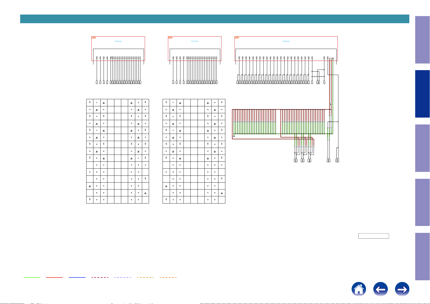
SCH15_IP OSD DDR
All Ref.No. has been described in the parts list are four digits.
But there are less than four digits of printed Ref.No. on the PCB, and they have become four digits after the header by adding "0" in the parts list.
Caution in
servicing
8G
DR_TXDQS0
DDR1
F7
DR_TXDQS0
1A2 3 4 5 6 7 8 9
A1
1A22
DDR_1.8V
B110B211B3
B
DR_TXDQ14
DGND
C119C220C3
C
DR_TXDQ9
D128D229D3
D
DR_TXDQ12
DGND
E137E238E3
E
DDR_1.8V
F146F247F3
F
DR_TXDQ6
G155G256G3
G
DDR_1.8V
DR_TXDQ1
H164H265H3
H
DR_TXDQ4
DGND
J173J274J3
J
DDR_1.8V DDR_1.8V
K283K3
K
DR_TXCKE
91
L1
L292L3
L
DR_TXBA2 DR_TXBA0
101M3102
M2
M
DR_TXA10
109N2110N3111
N1
N
DR_TXA3
DGND
119P3120
P2
P
DR_TXA7
127R2128R3129
R1
R
DDR_1.8V
DR_TXA12
TO G8
TO IP/OSD
TO 8U-310223(14/19)
DR_TXDQSB1
DR_TXDQSB0
DR_TXDQ0
DR_TXDM0
DR_TXDQ1
DR_TXDQ2
DR_TXDM1
DR_TXDQ4
DR_TXDQS1
DDR1
DDR1
E8
B7
DR_TXDQS1
DR_TXDQSB0
A3
DGND
DR_TXDM1
DDR_1.8V
DR_TXDQ11
DGND
DR_TXDM0
DDR_1.8V
DR_TXDQ3
DGND
DR_TXWEB
DR_TXDQ3
DDR1
DDR1
DDR1
DDR1
DDR1
DDR1
A8
DR_TXDQSB1
F3
DR_TXDM0
DDR1
B3
DR_TXDM1
G8
DR_TXDQ0
G2
DR_TXDQ1
H7
DR_TXDQ2
H3
DR_TXDQ3
H1
DR_TXDQ4
DDR1
DDR1
3
12
21
30
39
48
57
66
75
84
93
DR_TXBA1
DR_TXA1
DR_TXA5
DR_TXA9
DR_1_RFU1
U3000
A3R12E40DBF-8E
DR_TXDQ7
DR_TXDQ6
DR_TXDQ9
DR_TXDQ8
DR_TXDQ5
DDR1
DDR1
DDR1
DDR1
DDR1
F9
C2
C8
H9
F1
DR_TXDQ7
DR_TXDQ9
DR_TXDQ8
DR_TXDQ5
DR_TXDQ6
A77A88A9
DGND
B716B817B9
DR_TXDQS1
C725C826C9
DDR_1.8VDDR_1.8V
D734D835D9
DR_TXDQ10
E743E844E9
DGND
F752F853F9
DR_TXDQS0
G761G862G9
DDR_1.8V
H770H871H9
DR_TXDQ2
J779J880J9
DGND
K788K889K9
DR_TXRASB
L797L8
DR_TXCASB
M7
DR_TXA2
N7
DR_TXA6
P7
DR_TXA11
R7
DR_1_RFU2
DR_TXDQ14
DR_TXDQ11
DR_TXDQ12
DR_TXDQ10
DR_TXDQ13
DR_TXDQ15
DDR1
DDR1
DDR1
DDR1
DDR1
D3
D1
B9
B1
D9
D7
DR_TXDQ11
DR_TXDQ12
DR_TXDQ15
DR_TXDQ14
DR_TXDQ13
DR_TXDQ10
DDR_1.8V
DR_TXDQSB1
DR_TXDQ15
DGND
DDR_1.8V
DR_TXDQ8
DR_TXDQ13
DGND
DDR_1.8V
DR_TXDQSB0
DR_TXDQ7
DGND
DDR_1.8V
DR_TXDQ0
DR_TXDQ5
DGND
DDR_1.8V
DR_TXCK
DR_TXCKB
DDR_1_ODT
98
DR_TXCSB
106M8107M9108
DDR_1.8V
DR_TXA0
115N8116
DR_TXA4
124P8125P9126
DR_TXA8
DGND
133R8134
DR_1_RFU3
9
18
B
27
C
36
D
45
E
54
F
63
G
72
H
81
J
90
K
L
M
N
P
R
IP/OSD 1st DDR
9G
DR_TXDQS2
DDR2
F7
DR_TXDQS2
1A2 3 4 5 6 7 8 9
A11A22A3
DDR_1.8V
B110B211B3
DR_TXDQ30
DGND
C119C220C3
DDR_1.8V
DR_TXDQ25
D128D229D3
DR_TXDQ28
DGND
E137E238E3
-
-
DDR_1.8V
F146F247F3
DR_TXDQ22
DGND
G155G256G3
DDR_1.8V
DR_TXDQ17
H164H265H3
DR_TXDQ20
DGND
J173J274J3
TX_DDRVREFTX_DDRVREF
K283K3
DR_TXCKE
91
L292L3
L1
DR_TXBA0
DR_TXBA2
101M3102
M2
DR_TXA10
110N3111
N1
N2
109
DR_TXA3
DGND
119P3120
P2
DR_TXA7
127R2128R3129
R1
DDR_1.8V
DR_TXA12
TO G9
TO IP/OSD
TO 8U-310223(14/19)
DR_TXDQ21
DR_TXDQ20
DR_TXDQ17
DR_TXDQ18
DR_TXDQ16
DR_TXDQSB2
DDR2
E8
DR_TXDQSB2
DR_TXDQS3
DDR2
DR_TXDQS3
DR_TXDQ19
DR_TXDQSB3
DR_TXDM3
DR_TXDM2
DDR2
DDR2
DDR2
DDR2
DDR2
DDR2
DDR2
A8
DR_TXDQSB3
F3
DR_TXDM2
B3
DR_TXDM3
G8
DR_TXDQ16
G2
DR_TXDQ17
H7
DR_TXDQ18
H3
DR_TXDQ19
DDR2
H1
DR_TXDQ20
DR_TXDQ21
DDR2
B7
3
DGND
12
DR_TXDM3
21
DDR_1.8V
30
DR_TXDQ27
39
DGND
48
DR_TXDM2
57
DDR_1.8V
66
DR_TXDQ19
75
DGND
84
DR_TXWEB
93
DR_TXBA1
DR_TXA1
DR_TXA5
DR_TXA9
DR_2_RFU1
U3001
A3R12E40DBF-8E
IP/OSD 2nd DDR
DR_TXDQ24
DR_TXDQ22
DR_TXDQ23
DR_TXDQ25
DDR2
DDR2
DDR2
DDR2
DDR2
H9
C8
C2
F1
F9
DR_TXDQ24
DR_TXDQ25
DR_TXDQ22
DR_TXDQ23
A77A88A9
DGND
B716B817B9
DR_TXDQS3
C725C826C9
DDR_1.8V
D734D835D9
DR_TXDQ26
E743E844E9
DGND
F752F853F9
DR_TXDQS2
G761G862G9
DDR_1.8V
H770H871H9
DR_TXDQ18
J779J880J9
DGND
K788K889K9
DR_TXRASB
L797L8
DR_TXCASB
M7
DR_TXA2
N7
DR_TXA6
P7
DR_TXA11
R7
DR_TXDQ29
DR_TXDQ28
DR_TXDQ27
DR_TXDQ26
DDR2
DDR2
DDR2
D9
D7
D3
D1
DR_TXDQ29
DR_TXDQ26
DR_TXDQ27
DR_TXDQ28
DR_TXDQSB3
DGND
DR_TXDQ24
DGND
DR_TXDQSB2
DGNDDGND
DR_TXDQ16
DGND
DR_TXCK
DR_TXCKB
DR_TXCSB
106M8107M9108
DR_TXA0
115N8116
DR_TXA4
124P8125P9126
DR_TXA8
133R8134
DR_2_RFU3DR_2_RFU2
DR_TXDQ30
DDR2
B1
DR_TXDQ30
DR_TXDQ31
DDR2
B9
DR_TXDQ31
DR_TXDQ29
DR_TXDQ23
98
9
DDR_1.8V
18
DR_TXDQ31
27
DDR_1.8V
36
45
DDR_1.8V
54
63
DDR_1.8V
72
DR_TXDQ21
81
DDR_1.8V
90
DDR_2_ODT
DDR_1.8V
DGND
10/6.3
X5R
C3000
DGND
0H
DDR1
0.1
0.1
C3001
C3002
DDR2
L2
DR_TXBA0
0.1
DR_TXBA0
DDR1
L2
DR_TXBA0
0.1
C3004
C3003
DDR2
L3
DR_TXBA1
DR_TXBA1
DDR1
L3
DR_TXBA1
0.1
0.1
C3005
C3006
DDR2
L1
DR_TXBA2
0.1
C3007
DR_TXBA2
DDR1
L1
DR_TXBA2
0.1
C3008
K7
DR_TXRASB
DR_TXRASB
DDR2
K7
DR_TXRASB
0.1
C3009
DDR1
DDR2
L7
DR_TXCASB
0.1
0.1
C3010
C3011
DR_TXCASB
DDR1
L7
DR_TXCASB
0.1
C3012
K3
DR_TXWEB
DR_TXWEB
DR_TXA1
DR_TXCKE
DDR2
K2
DR_TXCKE
DDR1
M8
DR_TXA0
DR_TXA0
DDR1
DDR2
M8
DR_TXA0
M3
DR_TXA1
DDR2
M3
DR_TXA1
DDR1
M7
DR_TXA2
DR_TXA2
DDR2
M7
DR_TXA2
DDR1
N2
DR_TXA3
DR_TXA3
DDR2
N2
DR_TXA3
DDR2
K3
DR_TXWEB
DDR1
L8
DR_TXCSB
DR_TXCSB
DDR2
L8
DR_TXCSB
DDR1
K2
DR_TXCKE
IP/OSD 1st&2nd ADD/cntl
1000P
1000P
1000P
1000P
1000P
1000P
0.1
C3016
C3015
1000P
C3018
C3017
C3020
C3019
C3022
C3021
1000P
C3023
C3024
0.1
0.1
C3014
C3013
0.1
TO H0
TO IP/OSD
TO 8U-310223(14/19)
DR_TXA5
DR_TXA6
DR_TXA4
DDR2
DDR1
DDR2
DDR1
DDR2
DDR1
DDR1
N8
N7
N7
N8
N3
N3
DR_TXA4
DR_TXA6
DR_TXA6
DR_TXA4
DR_TXA5
DR_TXA5
0.1
0.1
0.1
0.1
10/6.3
X5R
C3026
C3029
C3027
C3028
C3025
DR_TXA8
DR_TXA7
DR_TXA9
DDR2
DDR2
DDR1
DDR2
DDR1
P3
P8
P3
P2
P2
P8
DR_TXA8
DR_TXA9
DR_TXA7
DR_TXA9
DR_TXA7
DR_TXA8
0.1
0.1
0.1
0.1
0.1
C3032
C3033
C3031
C3034
C3030
OPEN
OPEN
OPEN
R3001
R3000
R3002
DDR2
DDR1
DR_1_RFU1R3DR_2_RFU1R3DR_2_RFU2
DR_TXA11
DR_TXA12
DR_TXA10
DDR2
DDR1
DDR2
DDR1
DDR2
DDR1
M2
R2
P7
M2
R2
P7
DR_TXA10
DR_TXA12
DR_TXA11
DR_TXA10
DR_TXA12
DR_TXA11
0.1
0.1
0.1
0.1
0.1
0.1
0.1
C3041
C3035
C3039
C3036
C3037
C3040
C3038
OPEN
OPEN
OPEN
OPEN
OPEN
OPEN
OPEN
R3005
R3004
R3009
R3008
R3003
R3007
R3006
DDR1
DDR2
DDR2
DDR1
R7
R8
DR_1_RFU2R7DR_1_RFU3R8DR_2_RFU3
DR_TXCK
R3011
OPEN
DDR1
J8
DR_TXCK
1000P
1000P
C3043
C3042
OPEN
OPEN
R3012
R3010
DDR1
1000P
1000P
C3044
C3045
DDR2
K8
J8
DR_TXCK
DR_TXCKB
1000P
C3046
R3013
OPEN
1000P
C3047
DDR2
1000P
1000P
C3048
C3049
DR_TXCKB
K8
DR_TXCKB
TX_DDRVREF
DDR_1.8V
DV1.8V
DGND
L3000
BLM21PG221
OPEN
1K
0.5%
R3016
C3051
1K
0.1
1u
0.5%
C3050
C3052
R3017
10K
10K
R3014
R3015
DDR2
DDR1
K9
K9
DDR_1_ODT
DDR_2_ODT
DDR1
DDR2
J2
Electrical Mechanical Repair Information Updating
TX_DDRVREFJ2TX_DDRVREF
GND LINE
POWER+ LINE
POWER- LINE
AUDIO SIGNAL
TMDS SIGNAL
ANALOG VIDEO
DIGITAL VIDEO
24
8U-310223(15/19)
DIGITAL_UNIT
IP/OSD DDR
Condential
Page 25
SCH16_VIDEO PLD
All Ref.No. has been described in the parts list are four digits.
But there are less than four digits of printed Ref.No. on the PCB, and they have become four digits after the header by adding "0" in the parts list.
Caution in
servicing
H2
TO NET MODULE CONNECT
NETGUI_PCK.
NETGUI_HS.
NETGUI_VS.
NETGUI_DE.
NETGUI_R7.
NETGUI_R6.
NETGUI_R5.
NETGUI_R4.
NETGUI_R3.
NETGUI_R2.
NETGUI_R1.
NETGUI_R0.
NETGUI_G7.
NETGUI_G6.
NETGUI_G5.
NETGUI_G4.
TO 8U-310223(19/19)
NETGUI_G3.
NETGUI_G2.
NETGUI_G1.
NETGUI_G0.
NETGUI_B7.
NETGUI_B6.
NETGUI_B5.
NETGUI_B4.
NETGUI_B3.
NETGUI_B2.
NETGUI_B1.
NETGUI_B0.
TO 2H
R3223
R3230
R3229
R3229
R3229
R3232
R3235
R3230
R3235
R3230
R3235
R3230
R3229
R3233
R3234
R3232
R3234
R3232
R3234
R3232
R3235
R3231
R3231
R3233
R3231
R3233
R3231
R3233
R3234
1A2 3 4 5 6 7 8 9
A11A22A33A44A55A66A77A8
.PO8KI_Y5/R1
DGND
B117B218B319B420B521B622B723B8
B
.PO8KI_Y8/R4
DGND
C133C234C335C436C537C638C739C8
C
.PO8KI_Y9/R5
DV3.3V
D149D250D351D452D553D654D755D8
D
.PO8KI_PCK
.PO8KI_VSYNC
E165E266E367E468E569E670E771E8
E
.PO8KI_HSYNC
8KOPI_C2/B2
F181F282F383F484F585F686F787F8
10
NETGUI_PCK
J5
7
8
10x4
NETGUI_HS
R3
3
4
10x4
NETGUI_VS
R12
6
5
10x4
NETGUI_DE
T12
2
1
10x4
8
7
10x4
NETGUI_R7
P5
5
6
10x4
NETGUI_R6
P10
2
1
10x4
NETGUI_R5
T4
3
4
10x4
NETGUI_R4
T11
3
4
10x4
NETGUI_R3
R4
2
1
10x4
NETGUI_R2
R11
5
6
10x4
NETGUI_R1
P4
8
7
10x4
NETGUI_R0
P11
8
7
10x4
NETGUI_G7
R6
5
6
10x4
NETGUI_G6
R9
2
1
10x4
NETGUI_G5
P6
3
4
10x4
NETGUI_G4
P9
3
4
10x4
NETGUI_G3
T5
2
1
10x4
NETGUI_G2
T10
5
6
10x4
NETGUI_G1
R5
8
7
10x4
NETGUI_G0
R10
8
7
10x4
NETGUI_B7
T7
6
5
10x4
NETGUI_B6
P8
1
2
10x4
NETGUI_B5
R7
3
4
10x4
NETGUI_B4
R8
4
3
10x4
NETGUI_B3
P7
2
1
10x4
NETGUI_B2
T8
5
6
10x4
NETGUI_B1
T6
7
8
10x4
NETGUI_B0
T9
F
8KOPI_C3/B3
8KOPI_HSYNC
G197G298G399G4
G
8KOPI_C8/G0
8KOPI_C11/G3
H1
113H2114H3115H4116H5117H6118H7119H8120H9121
H
8KOPI_Y6/R2
8KOPI_Y3/G7
J1
129J2130J3131J4132J5133J6134J7135J8136J9137
J
8KOPI_C6/B6
8KOPI_C5/B5
K1
145K2146K3147K4148K5149K6150K7151K8152K9153
K
8KOPI_Y1/G5
8KOPI_C10/G2
L1
161L2162L3163L4164L5165L6166L7167L8168L9169
L
8KOPI_Y4/R0
8KOPI_Y5/R1
M1
177M2178M3179M4180M5181M6182M7183M8184M9185
M
8KOPI_Y7/R3
8KOPI_Y8/R4
193N2194N3195N4196N5197N6198N7199N8200N9201
N1
N
8KOPI_Y11/R7
8KOPI_DE
209P2210P3211P4212P5213P6214P7215P8216P9217
P1
P
8KOPI_VSYNC
DV3.3V
225R2226R3227R4228R5229R6230R7231R8232R9233
R1
R
DGND DGND
241T2242T3243T4244T5245T6246T7247T8248T9249
T1
T
DGND
U3200
.PO8KI_C3/B3
.PO8KI_C10/G2
DV3.3V
.PO8KI_Y3/G7
.PO8KI_C11/G3
.PO8KI_C6/B6
.PO8KI_Y4/R0
.PO8KI_Y2/G6
.PO8KI_C7/B7
.PO8KI_Y11/R7
.PO8KI_Y0/G4
.PO8KI_Y6/R2
.PO8KI_DE
.PO8KI_Y7/R3
.PO8KI_Y10/R6
100G5101G6102G7103G8104G9105
8KOPI_C7/B7
8KOPI_Y0/G4
8KOPI_C9/G1
8KOPI_Y2/G6
8KOPI_C0/B0
8KOPI_Y9/R5
8KOPI_C1/B1
NETGUI_HS
CKIN
8KOPI_PCK
CKIN CKIN
NETGUI_PCK
8KOPI_C4/B4
O
VP_TDO
8KOPI_Y10/R6
M
VP_TMS
K
VP_TCK
NETGUI_R1
NETGUI_R7
NETGUI_G1
NETGUI_R3
NETGUI_G3
NETGUI_R5
DV3.3V
EPM570F256C4N
.PO8KI_C5/B5
.PO8KI_C0/B0
.PO8KI_Y1/G5
.PO8KI_C1/B1
.PO8KI_C4/B4
DGND
.PO8KI_C8/G0 .POHI_Y11/G7
.PO8KI_C9/G1
.PO8KI_C2/B2
DGND
DV3.3V
DGND
DV3.3V
DV3.3V
DGND
I
VP_TDI
NETGUI_G5
NETGUI_B3
NETGUI_G7
NETGUI_B5
NETGUI_B7
NETGUI_B1
10 11 12 13 14 15 16
8A99
A1010A1111A1212A1313A1414A1515A16
.POHI_DE
.POHI_C11/R7
24B925
B1026B1127B1228B1329B1430B1531B16
.POHI_HSYNC
.POHI_C10/R6
40C941
C1042C1143C1244C1345C1446C1547C16
.POHI_C9/R5
.POHI_VSYNC .POHI_C0/B4
56D957
D1058D1159D1260D1361D1462D1563D16
72E973
E1074E1175E1276E1377E1478E1579E16
88F989
F1090F1191F1292F1393F1494F1595F16
DV3.3VDV3.3V
106
G10
DGND
DGND
DGND
H10
DGND
DV3.3V
DGND
DV3.3V
NETGUI_G4
NETGUI_G6
NETGUI_B0
J10
K10
L10
M10
N10
P10
NETGUI_R6
R10
NETGUI_G0
T10
NETGUI_G2
DGND
DGND
122
138
154
170
186
202
218
234
250
DV3.3V DV3.3V
DGND
DGND
DV3.3V
NETGUI_B6
NETGUI_B4
NETGUI_B2
.POHI_C8/R4
.POHI_C7/R3
.POHI_C6/R2
G11
H11
DV3.3V
J11
DV3.3V
K11
L11
M11
N11
P11
NETGUI_R0
R11
NETGUI_R2
T11
NETGUI_R4
107
123
139
155
171
187
203
219
235
251
.POHI_C5/R1
.POHI_C4/R0
G12
CKIN
H12
J12
HOPI_PCK
K12
L12
M12
N12
VPLD_TRANS2
P12
HOPI_Y0/B0
R12
NETGUI_VS
T12
NETGUI_DE
108
124
140
156
172
188
204
220
236
252
.POHI_Y10/G6
.POHI_Y9/G5
.POHI_Y8/G4
G13
H13
J13
K13
L13
VPLD_TRANS1
M13
HOPI_Y6/G2
N13
TTL_SELA
P13
HOPI_Y3/B3
R13
HOPI_Y2/B2
T13
HOPI_Y1/B1
109
125
141
157
173
189
205
221
237
253
DV3.3V
.POHI_Y0/B0
.POHI_Y1/B1
.POHI_C3/B7
.POHI_Y6/G2
G14
HOPI_DE
H14
HOPI_C11/R7
J14
HOPI_C7/R3
K14
HOPI_C4/R0
L14
VPLD_TRANS0
M14
HOPI_Y7/G3
N14
TTL_SELB
P14
SD/HD
R14
HOPI_C0/B4
T14
DV3.3V
110
126
142
158
174
190
206
222
238
254
.POHI_Y2/B2
DGND
.POHI_C1/B5
.POHI_Y4/G0
.POHI_Y7/G3
G15
HOPI_VSYNC
H15
HOPI_C10/R6
J15
K15
HOPI_C5/R1
L15
HOPI_Y10/G6
M15
HOPI_Y9/G5
N15
HOPI_Y4/G0
P15
HOPI_C3/B7
R15
T15
HOPI_C1/B5
111
127
143
159
175
191
207
223
239
255
DGND
.POHI_Y3/B3
DV3.3V
.POHI_C2/B6
.POHI_Y5/G1
.POHI_PCK
G16
HOPI_HSYNC
H16
HOPI_C9/R5
J16
HOPI_C8/R4
K16
HOPI_C6/R2
L16
HOPI_Y11/G7
M16
HOPI_Y8/G4
N16
HOPI_Y5/G1
P16
DV3.3V
R16
HOPI_C2/B6
T16
DGND
16
32
0.1
0.1
C3205
C3206
M5
N4
L6
P3
0.1
C3207
0.1
0.1
C3211
C3209
0.1
0.1
C3213
C3214
0.1
1000P
C3215
C3216
R3218
R3218
R3218
R3218
1000P
C3217
1000P
C3218
48
64
80
96
112
128
144
160
176
192
208
224
240
256
DV3.3V
VPLD_TRANS2
VPLD_TRANS1
VPLD_TRANS0
TTL_SELB
TTL_SELA
SD/HD
VP_TDO
VP_TMS
VP_TDI
VP_TCK
0.1
0.1
C3203
C3204
N12
L13
L14
N14
N13
P14
3 4
5 6
1 2
7 8
1000P
C3219
10x4
10x4
10x4
10x4
1000P
1000P
C3220
C3221
2D
7F
7C
SUB_TDO
SUB_TMS
.TDO1_TDI2
SUB_TCK
DV3.3V
DGND
VPLD_TRANS2
VPLD_TRANS1
VPLD_TRANS0
TTL_SELB
TTL_SELA
SD/HD
TO A.PLD
TO 8U-310223(4/19)
TO D2
TO HDMI
SUPPLY
TO 8U-310223(10/19)
TO F7
TO EXPANDER
TO 8U-310223(3/19)
TO C7
Electrical Mechanical Repair Information Updating
47K
R3222
GND LINE
POWER+ LINE
POWER- LINE
8KOPI_VSYNCP28KOPI_HSYNC
8KOPI_Y11/R7
8KOPI_DEN28KOPI_Y9/R5
8KOPI_PCK
F2
N1
H5
7G
8KOPI_DE
8KOPI_PCK
8KOPI_VSYNC
8KOPI_HSYNC
8KOPI_Y11/R7
AUDIO SIGNAL
8KOPI_Y10/R6
M2
M4
M3
8KOPI_Y8/R4
8KOPI_Y7/R3
8KOPI_Y9/R5
8KOPI_Y10/R6
H1
8KOPI_Y6/R2
8KOPI_Y4/R0
8KOPI_Y5/R1
K2
H2
8KOPI_Y3/G7
8KOPI_Y1/G5
8KOPI_Y2/G6
K1
H3
8KOPI_Y0/G4
8KOPI_C11/G3
8KOPI_C10/G2
8KOPI_C10/G2
8KOPI_Y1/G5
8KOPI_Y5/R1L28KOPI_C11/G3G18KOPI_C9/G1J38KOPI_C2/B2
8KOPI_Y8/R4M18KOPI_Y6/R2
8KOPI_Y7/R3
8KOPI_Y2/G6K38KOPI_Y0/G4
8KOPI_Y4/R0L18KOPI_Y3/G7
TMDS SIGNAL
HOPI_C11/R7
HOPI_HSYNC
HOPI_C8/R4
HOPI_C7/R3
HOPI_VSYNC
HOPI_PCK
HOPI_DE
HOPI_C10/R6
HOPI_C9/R5
8KOPI_C7/B7
8KOPI_C6/B6
8KOPI_C8/G0
G3
J2
G2
8KOPI_C3/B3
8KOPI_C4/B4L48KOPI_C1/B1
8KOPI_C5/B5
E2
F1
N3
J1
8KOPI_C0/B0
.PO8KI_VSYNCD2.PO8KI_Y10/R6F3.PO8KI_Y3/G7B3.PO8KI_Y1/G5A7.PO8KI_C11/G3
.PO8KI_Y9/R5C2.PO8KI_Y7/R3
.PO8KI_Y8/R4
.PO8KI_Y11/R7D3.PO8KI_Y4/R0C3.PO8KI_C5/B5
.PO8KI_DE
.PO8KI_Y6/R2D4.PO8KI_Y5/R1A2.PO8KI_Y2/G6
.PO8KI_HSYNC
.PO8KI_PCK
L3
10x4
1 2
R3203
D1
47
R3214
E1
10x4
10
3 4
R3203
R322510R3226
E4
B1
E3
10x4
7 8
R3200
10x4
5 6
R3200
10x4
5 6
R3203
10x4
7 8
R3203
10x4
1 2
R3200
10x4
3 4
R3200
10x4
1 2
R3204
10x4
3 4
R3204
10x4
5 6
R3204
10x4
7 8
R3204
C4
10x4
3 4
R3201
.PO8KI_Y0/G4D5.PO8KI_C9/G1
.PO8KI_C8/G0
.PO8KI_C7/B7
.PO8KI_C6/B6
.PO8KI_C10/G2
C8
B4
A4
C7
C5
B5
10x4
10x4
10x4
10x4
10x4
10x4
10x4
1 2
7 8
1 2
7 8
5 6
3 4
5 6
R3201
R3201
R3205
R3205
R3205
R3201
R3205
.PO8KI_C4/B4
A8
B8
10x4
10
1 2
R3206
R322710R3228
.PO8KI_C1/B1
.PO8KI_C2/B2
.PO8KI_C0/B0
.PO8KI_C3/B3
B6
C6
A6
A5
10x4
10x4
10x4
3 4
7 8
5 6
R3206
R3206
R3206
J12
HOPI_C6/R2
HOPI_Y11/G7
HOPI_C5/R1
HOPI_C4/R0
H14
G16
J16
J14
G15
G14
L16
K15
H15
H16
K14
K16
HOPI_Y9/G5
HOPI_Y7/G3
HOPI_Y10/G6
HOPI_Y8/G4
M15
M14
L15
M16
HOPI_Y5/G1
HOPI_Y6/G2
HOPI_C3/B7
HOPI_Y4/G0
N16
M13
P15
N15
HOPI_C2/B6
R16
H3
PO8KI_DE
PO8KI_PCK
PO8KI_VSYNC
8KOPI_C1/B1
PO8KI_HSYNC
8KOPI_C5/B5
8KOPI_C2/B2
8KOPI_C7/B7
8KOPI_C3/B3
8KOPI_C4/B4
8KOPI_C8/G0
8KOPI_C9/G1
8KOPI_C6/B6
TO IP/OSD
TO 8U-310223(14/19) TO 8U-310223(17/19)
8KOPI_C0/B0
TO G7
PO8KI_Y9/R5
PO8KI_Y10/R6
PO8KI_Y11/R7
ANALOG VIDEO
PO8KI_Y5/R1
PO8KI_Y8/R4
PO8KI_Y7/R3
PO8KI_Y2/G6
PO8KI_Y3/G7
PO8KI_Y6/R2
PO8KI_Y4/R0
DIGITAL VIDEO
PO8KI_Y0/G4
PO8KI_Y1/G5
PO8KI_C10/G2
PO8KI_C11/G3
PO8KI_C8/G0
PO8KI_C9/G1
PO8KI_C7/B7
PO8KI_C6/B6
PO8KI_C4/B4
PO8KI_C5/B5
PO8KI_C1/B1
PO8KI_C2/B2
PO8KI_C0/B0
PO8KI_C3/B3
DGND
HOPI_PCK
HOPI_HSYNC
HOPI_VSYNC
HOPI_DE
HOPI_C9/R5
HOPI_C8/R4
HOPI_C10/R6
HOPI_C11/R7
HOPI_C4/R0
HOPI_C5/R1
HOPI_C7/R3
HOPI_C6/R2
HOPI_Y8/G4
HOPI_Y9/G5
HOPI_Y11/G7
HOPI_Y10/G6
HOPI_Y5/G1
HOPI_Y7/G3
HOPI_Y4/G0
HOPI_Y6/G2
HOPI_C3/B7
HOPI_C2/B6
25
HOPI_C0/B4
HOPI_C1/B5
HOPI_Y2/B2
HOPI_Y3/B3
HOPI_Y1/B1
R14
T15
R13
P13
T13
HOPI_C0/B4
HOPI_C1/B5
HOPI_Y1/B1
HOPI_Y3/B3
HOPI_Y2/B2
TO HDMI TX
.POHI_PCK
HOPI_Y0/B0
.POHI_HSYNCB9.POHI_C8/R4
F16
P12
22x4
22x4
22x4
22
7 8
1 2
5 6
R3208
R3208
R3208
R3224
POHI_PCK
POHI_HSYNC
HOPI_Y0/B0
TO 3H
.POHI_DE
.POHI_C11/R7
.POHI_VSYNC
A9
C9
A10
22x4
22x4
1 2
3 4
R3215
R3208
POHI_DE
POHI_VSYNC
POHI_C11/R7
.POHI_C7/R3
.POHI_C10/R6
.POHI_C9/R5
B11
B10
A11
C10
22x4
22x4
22x4
22x4
5 6
3 4
1 2
7 8
R3215
R3215
R3216
R3215
POHI_C7/R3
POHI_C8/R4
POHI_C9/R5
POHI_C10/R6
.POHI_C5/R1
.POHI_C6/R2
.POHI_C4/R0
A12
C11
B12
22x4
22x4
22x4
3 4
7 8
5 6
R3216
R3216
R3216
POHI_C4/R0
POHI_C5/R1
POHI_C6/R2
.POHI_Y9/G5
.POHI_Y11/G7
.POHI_Y8/G4
.POHI_Y10/G6
B13
C12
C13
A13
22x4
22x4
22x4
22x4
3 4
7 8
5 6
1 2
R3210
R3210
R3210
R3210
POHI_Y9/G5
POHI_Y8/G4
POHI_Y10/G6
POHI_Y11/G7
.POHI_Y7/G3
.POHI_Y5/G1
.POHI_Y6/G2
F15
E16
F14
10x4
10x4
10x4
7 8
5 6
3 4
R3212
R3212
R3212
POHI_Y5/G1
POHI_Y6/G2
POHI_Y7/G3
.POHI_Y4/G0
.POHI_C3/B7
.POHI_C2/B6
E15
E14
D16
10x4
10x4
10x4
5 6
7 8
1 2
R3213
R3213
R3212
POHI_Y4/G0
POHI_C2/B6
POHI_C3/B7
.POHI_C1/B5
.POHI_Y3/B3
.POHI_C0/B4
D15
B16
C15
10x4
10x4
10x4
7 8
1 2
3 4
R3207
R3213
R3213
POHI_Y3/B3
POHI_C1/B5
POHI_C0/B4
.POHI_Y1/B1
.POHI_Y0/B0
.POHI_Y2/B2
C14
B14
A15
10x4
10x4
10x4
1 2
3 4
5 6
R3207
R3207
R3207
POHI_Y1/B1
POHI_Y0/B0
POHI_Y2/B2
VIDEO PLD
8U-310223(16/19)
DIGITAL_UNIT
Condential
Page 26
SCH17_HDMI TX
8F
CEC_STBY5V
CEC_STBY3.3V
CEC5V
CEC3.3V
FBMJ3216HL160NT
6G
GND LINE
9D
TO D9
3G
TO G3
5G
TO G5
TO G6
N3403
TO N5501
1G
TO G1
CEC1.1V3
TO F8
TO HDMI SUPPLY
TO AUDIO PLD
TO HDMI SW2TO HDMI SW1
TO HDMI SW1
A0D7ABAR1990
UTILITY/HEAC+
To_8U-210228-5(N5501)
FRONT_HDMI_USB_UNIT
TO Decoder
POWER+ LINE
L3401
DGND
OPEN.
C3411
TO 8U-310223(10/19)
L3406
BLM21PG221
4.7u
C3499
C9500
L3404
BLM21PG221
4.7u
C3497
RX256fs/DSDMCK
RX64fs/DSDSCK
RXSPDIF/DSD0
RXI2S0/DSD1
RXI2S1/DSD2
RXI2S2/DSD3
RXI2S3/DSD4
RXfs/DSD5
TX64fs
TO 8U-310223(4/19)
TXfs
TXI2S0
P0_C-
P0_C+
P0_D0P0_D0+
P0_D1P0_D1+
P0_D2P0_D2+
P0_DDCCL
P0_DDCDA
P2_C-
P2_C+
P2_D0P2_D0+
P2_D1P2_D1+
P2_D2P2_D2+
TO 8U-310223(13/19) TO 8U-310223(12/19)
P2_DDCCL
P2_DDCDA
CEC_COM
RXF_5V
TO 8U-310223(13/19)
N3403
19
HPD/HEAC-
18
+5V
17
GND
16
DDCDATA
15
DDCCLK
14
13
CE_Remote
12
CK-
11
CKshield
10
CK+
9
D0-
8
DOshield
7
D0+
6
D1-
5
D1shield
4
D1+
3
D2-
2
D2shield
1
D2+
TX_C-
TX_C+
TX_0-
TX_0+
TX_1-
TX_1+
TX_2-
TX_2+
RXD_DDCCL
TO 8U-310223(11/19)
RXD_DDCDA
OPEN
4.7u
C3423
C3420
OPEN.
OPEN
4.7u
C3424
C3421
C3430
100/6.3
100/6.3
100/6.3
C9501
C9502
OPEN
4.7u
C3422
C3419
OPEN
R3413
0
R3406
POWER- LINE
C9503
100/6.3
100/6.3
C9504
C9505
C3484
100/6.3
FBMJ3216HL160NT
OPEN.C3412
L3402
BLM21PG221
L3403
BLM21PG221
4.7u
C3416
L3400
BLM21PG221
4.7u
100/6.3
C3406
C9506
L3408
BLM21PG221
4.7u
C3512
1000P
C3485
1000P
AUDIO SIGNAL
L3405
R3428
All Ref.No. has been described in the parts list are four digits.
But there are less than four digits of printed Ref.No. on the PCB, and they have become four digits after the header by adding "0" in the parts list.
Caution in
servicing
R3471
C3487
OPEN
OPEN
C3492
R3481
OPEN
R3484
R3480
10K
R3472
100K
OPEN
OPEN
OPEN
D3413
C3491
DGND
HDMI
OUT 2
1
2
3
4
5
6
7
8
9
10
11
12
13
CE_REMOTE
14
15
16
17
18
19
HDMI
OUT 1
1
2
3
4
5
6
7
8
9
10
11
12
CE_REMOTE
13
14
15
16
17
18
19
Varistor
NV73A1JTTE8.2
TX2+
TX2_SHLD
TX2TX1+
TX1_SHLD
TX1TX0+
TX0_SHLD
TX0TXC+
TXC_SHLD
TXC-
N.C.
DDC_SCK
DDC_SDA
GND
+5V
HP_DET
N3401
A0D7ABAR1990
TX2+
TX2_SHLD
TX2TX1+
TX1_SHLD
TX1TX0+
TX0_SHLD
TX0TXC+
TXC_SHLD
TXC-
N.C.
DDC_SCK
DDC_SDA
GND
+5V
HP_DET
N3402
A0D7ABAR1990
Electrical Mechanical Repair Information Updating
787AVDD11RX
TX64fs
TXI2S0
787AVDD33RX
R3463
R3455
R3456
3
1
3
1
3
1
3
1
R3402
1M
0
0
3
1
3
1
3
1
3
1
OPEN.
UDZS5.1B
10K
D3428
D3409
R3474
R3465
0x2
4
2
R3452
0x2
4
2
R3466
0x2
4
2
R3453
EXC24CH900U
4
2
eARC+
eARC_HPD
R3403
47K
R3404
1M
Q3403
2SC4617EB
OPEN
1.8K
D3402
R3461
1.8K
R3462
D3429 OPEN.
R3405
220K
0x2
4
2
R3450
0x2
4
2
R3464
0x2
4
2
R3451
EXC24CH900U
4
2
OPEN.
OPEN
1.8K
OPEN.
OPEN.
D3407
D3411
D3400
D3405
R3468
1.8K
OPEN
OPEN
R3469
D3408 OPEN.
D3401
D3406 OPEN.
D3403
C3489
C3489
C3492
R3481
R3480
R3484
D3410
R3424
R3475
R3415
R3467
1.2K
100K
220P
3.3K
R3487
C3413
R3473
OPEN.
D3414
D3412 OPEN.
OPEN
R3454
R3459
0.1
C3488
OPEN.
OPEN.
D3416
D3418
D3417 OPEN.
D3415 OPEN.
w
eARC
OPEN
OPEN
OPEN
OPEN
OPEN
OPEN
0
OPEN
47k
OPEN.
OPEN.
D3422
D3420
D3419 OPEN.
D3421 OPEN.
w/o
eARC
1uF
1uF
51
10
10
5.1B
OPEN
10k
OPEN
220K
27K
R3477
0
OPEN.
OPEN.
D3424
D3426
D3425 OPEN.
D3427 OPEN.
D3423 OPEN.
D3404
KDS160
Q3402
2SD2114K
D3430 OPEN.
PTX0_2+
POHI_C7/R3
POHI_C6/R2
POHI_C5/R1
POHI_C4/R0
POHI_Y11/G7
POHI_Y10/G6
POHI_Y9/G5
POHI_Y8/G4
PTX0_C-
PTX0_C+
PTX0_2+
PTX0_2PTX0_1+
PTX0_1PTX0_0+
PTX0_0-
PTX1_C-
PTX1_C+
PTX1_2+
PTX1_2PTX1_1+
PTX1_1PTX1_0+
PTX1_0-
POHI_Y7/G3
POHI_Y6/G2
POHI_Y5/G1
POHI_Y4/G0
POHI_C3/B7
POHI_C2/B6
POHI_C1/B5
POHI_C0/B4
POHI_Y3/B3
POHI_Y2/B2
POHI_Y1/B1
POHI_Y0/B0
PTX0_HPD
PTX0_DDCSDA
PTX0_DDCSCL
PTX1_HPD
PTX1_DDCSDA
PTX1_DDCSCL
POHI_PCK
PTX0_2-
PTX0_1+
PTX0_1-
PTX0_0+
PTX0_0-
PTX0_C+
PTX0_C-
PTX0_DDCSCL
PTX0_DDCSDA
PTX0_HPD
PTX1_2+
PTX1_2-
PTX1_1+
PTX1_1-
PTX1_0+
PTX1_0-
PTX1_C+
PTX1_C-
PTX1_DDCSCL
PTX1_DDCSDA
PTX1_HPD
CEC_COM
CEC_OUT
CEC_IN
R3457
0
R3458
0
OPEN
0
R3416
R3424
H4
HPDout
HPDoutL
TO eARC
TO 8U-310223(18/19)
TO 4H
R3401
4.7K
Q3401
2SC4617EB
TX_2-
TX_2+
TX_1+
TX_1-
TX_0+
TX_0-
TX_C+
P2RX2M93P2RX2P
0.1
C3458
91
AVDD11RX2
89
P2RX1M90P2RX1P
0.1
C3460
88
AVDD11RX2
86
P2RX0M87P2RX0P
0.1
C3461
85
AVDD11RX2
TX_C-
83
0.1
C3457
82
P2RXCM84P2RXCP
RXF_0-
RXF_0+
RXF_2-
79
P3RX2M80P3RX2P
RXF_1+
0.1
C3463
78
AVDD11RX3
RXF_1-
76
P3RX1M77P3RX1P
0.1
C3465
75
AVDD11RX3
73
P3RX0M74P3RX0P
RXF_C+
0.1
C3467
72
AVDD11RX3
RXF_2+
81
VSS
AVDD33RX2
U3401
MN864787
VSS
/ Trans1
Q23
Q22
Q21
180
181
182
47x4
47x4
47x4
5 6
7 8
3 4
1 2
R3433
R3433
R3433
HOPI_C10/R6
HOPI_C9/R5
HOPI_C8/R4
Q20
183
0.1
C3459
VDD33IO
VDD11
Q19
Q18
Q17
184
185
186
187
0.1
47x4
47x4
47x4
7 8
5 6
3 4
C3454
R3434
R3434
R3434
HOPI_C6/R2
HOPI_C7/R3
HOPI_C5/R1
Q16
Q15
VSS
188
189
190
47x4
47x4
7 8
1 2
R3435
R3434
HOPI_C4/R0
HOPI_Y11/G7
VDD33IO
Q14
Q13
Q12
191
192
193
194
47x4
0.1
47x4
47x4
1 2
3 4
5 6
R3435
C3462
R3435
R3435
HOPI_Y8/G4
HOPI_Y10/G6
HOPI_Y9/G5
Q11
Q10
195
196
197Q9198Q8199Q7200Q6201
47x4
47x4
47x4
47x4
3 4
1 2
7 8
5 6
R3436
R3436
R3436
R3436
HOPI_Y4/G0
HOPI_Y6/G2
HOPI_Y5/G1
HOPI_Y7/G3
/ Trans2
47x4
47x4
7 8
5 6
R3437
R3437
HOPI_C3/B7
HOPI_C2/B6
RXF_C-
0.1
C3468
68
69
70
VSS
P3RXCM71P3RXCP
AVDD33RX3
/ Trans0
VSS
202Q5203Q4204
47x4
47x4
3 4
1 2
R3437
R3437
HOPI_C0/B4
HOPI_C1/B5
RX64fs/DSDSCK
0.1
0.1
33
R344133R342133R3426
C3505
C3470
66
67
VDD11
PVDD33
VDD33IO
205Q3206Q2207Q1208Q0209
47x4
47x4
0.1
7 8
5 6
R3440
R3440
C3464
HOPI_Y3/B3
HOPI_Y2/B2
POHI_DE
RXSPDIF/DSD0
RX256fs/DSDMCK
0.1
100x4
R3470
C3472
61
62
63
64
VDD33
CH0AMCLK65CH0ABCLK
CH0ASPDIF
216:
VDD11
210
0.1
0.1
47x4
47x4
1 2
3 4
C3469
C3466
R3440
R3440
HOPI_Y0/B0
HOPI_Y1/B1
POHI_HSYNC
100x4
R3470
DEIN
VDD33
211
82
R3443
TX0SCL
PCLKIN
POHI_VSYNC
POHI_C11/R7
POHI_C10/R6
100x4
100x4
100x4
78563434561278
R3470
R3444
R3444
59
VSYNCIN60HSYNCIN
TX1SCL
TX1SDA
VSS
214
212
213
POHI_C8/R4
POHI_C9/R5
100x4
100x4
100x4
12
R3470
R3444
R3444
55
D2056D2157D2258D23
D19
D18
D17
D16
D15
D14
D13
D12
VDD11
VSS
P0TXCM
AVDD11TX
P0TXCP
P0TX0M
AVDD33TX
P0TX0P
P0TX1M
AVDD11TX
P0TX1P
P0TX2M
AVDD11TX
P0TX2P
VDD11
VSS
P1TXCM
AVDD11TX
P1TXCP
P1TX0M
AVDD33TX
P1TX0P
P1TX1M
AVDD11TX
P1TX1P
P1TX2M
AVDD11TX
P1TX2P
VDD11
VSS
D11
D10
D9
D8
D7
VDD11
D6
VSS
D5
D4
D3
D2
D1
D0
TX0HPD
TX0SDA
TX1HPD
217
215
216
OPEN
R3475
100x4R3449
54
12
100x4R3449
53
34
100x4R3449
52
56
100x4R3449
51
78
100x4R3482
50
12
100x4R3482
49
34
100x4R3482
48
56
100x4R3482
47
78
0.1
C3471
46
45
44
0.1
C3473
43
42
41
0.1
C3476
40
39
38
0.1
C3477
37
36
35
0.1
C3478
34
33
0.1
C3511
32
31
30
0.1
C3479
29
28
27
0.1
C3480
26
25
24
0.1
C3481
23
22
21
0.1
C3515
20
19
0.1
C3482
18
17
82x4
R3476
16
12
82x4
R3476
15
34
82x4
R3476
14
56
82x4
R3476
13
78
82x4
R3479
12
12
0.1
C3483
11
82x4
R3479
10
34
9
82x4
R3479
8
56
82x4
R3479
7
78
82x4
R3460
6
12
82x4
R3460
5
34
82x4
R3460
4
56
82x4
R3460
3
78
2
1
RXF_5V
RXfs/DSD5
RXI2S3/DSD4
RXI2S2/DSD3
RXI2S1/DSD2
RXI2S0/DSD1
47K
10K
0.1
33
47K
10K
33x4
33x4
33x4
33x4
R3439
102
103
NIRQ0
HSCL1
HSDA0
VDD33
168
169
47
0.1
R3427
C3450
X3400
OPEN
C3510
R3442
101
CH0ALRCLK
SYSCLK/XI
170
R3418
27MHz
12P
C3434
345612
R3445
R3445
99
100
CH0ASD1
CH0ASD0
NC/XO
VSS
171
172
1M
1 3
R3445
VDD11
173
0.1
C3447
10P
C3435
0.1
78
C3453
R3445
92
94
95
97
VSS
VDD1196NIRQ1
CH0ASD398CH0ASD2
Slave Address:0x10
DEOUT
VSYNCOUT
HSYNCOUT
PCLKOUT
VDD33IO
174
175
176
177
178
179
47
47
47
0.1
47x4
C3456
R3429
R3430
R3431
R343347R3432
HOPI_VSYNC
HOPI_HSYNC
HOPI_DE
HOPI_PCK
HOPI_C11/R7
10K
10/6.3
10/6.3
2125
2125
R3422
C3455
C3516
C3518
R3423
R3420
C3517
10/6.3
2125
C3519
10/6.3
R3419
R3412
C3475
R3408
R3409
C3436
C3437
C3438
C3439
C3440
C3444
C3441
C3442
C3443
C3445
C3446
R3485
C3474
2125
47K
10K
R3410
0.1
10
10K
10K
0.1
0.1
0.1
0.1
0.1
0.1
0.1
0.1
0.1
0.1
0.1
10K
0.1
TX_HINT
787AVDD33Tx
787AVDD11Tx
787PVDD33
787VDD33
787VDD11
787VDD33IO
RXF_DDCDA
RXF_DDCCL
RXD_DDCDA
RXD_DDCCL
TX_HAINT
TXfs
P0_CP0_C+
P0_D0P0_D0+
P0_D1P0_D1+
P0_D2P0_D2+
P2_CP2_C+
P2_D0P2_D0+
P2_D1P2_D1+
P2_D2P2_D2+
TXI2S0
TXfs
TX64fs
P0_DDCDA
P0_DDCCL
P2_DDCDA
P2_DDCCL
HPD8
TX_RST
HSCL
HSDA
R3407
109
110
111
112
113
114
115
116
117
118
119
120
121
122
123
124
125
126
127
128
129
130
131
132
133
134
135
136
137
138
139
140
141
142
143
144
145
146
147
148
149
150
151
152
153
154
155
156
157
158
159
160
161
162
10
107
108
RX2P5V
RX1P5V
RX3SCL
RX2SDA
RX2SCL
NIRQA1
NIRQA0
VDD33
SCLK/LPSA1
MOSI/LPSA0
MISO
NCS
VDD11
VSS
AVDD33RX1
P1RXCM
P1RXCP
AVDD11RX1
P1RX0M
P1RX0P
AVDD11RX1
P1RX1M
P1RX1P
AVDD11RX1
P1RX2M
P1RX2P
VSS
AVDD33RX0
P0RXCM
P0RXCP
AVDD11RX0
P0RX0M
P0RX0P
AVDD11RX0
P0RX1M
P0RX1P
AVDD11RX0
P0RX2M
P0RX2P
VSS
VDD11
NOSDIRQ
CH1ASD0
CH1ALRCLK
CH1ABCLK
CH1ASPDIF
VDD33
VSS
RX1SDA
RX1SCL
RX0SDA
RX0SCL
TX0ARCIN
TX1ARCIN
164
163
47K
47K
R3414
R3415
R3411
1K
106
RX3P5V
NTEST
165
105
109:
110:
161:
162:
166
47
R3425
OPEN
C3509
VDD33
HSCL0
C3448 1000P
R3438
104
HSDA1
RX0P5V
RX3SDA
CEC
VDD11
NRESET
167
OPEN
4.7u
C3407
C3401
OPEN
4.7u
OPEN.
C3410
C3402
C3408
4.7u
OPEN
C3409
C3403
4.7u
C3400
4.7u
OPEN
C3514
C3513
RX256fs/DSDMCK
RX64fs/DSDSCK
RXSPDIF/DSD0
RXI2S0/DSD1
RXI2S1/DSD2
RXI2S2/DSD3
RXI2S3/DSD4
RXfs/DSD5
P0_C-
P0_C+
P0_D0P0_D0+
P0_D1P0_D1+
P0_D2P0_D2+
P0_DDCCL
P0_DDCDA
P2_C-
P2_C+
P2_D0P2_D0+
P2_D1P2_D1+
P2_D2P2_D2+
P2_DDCCL
P2_DDCDA
RXF_5V
RXF_DDCDA
RXF_DDCCL
47K
RXF_C-
RXF_C+
RXF_0-
RXF_0+
RXF_1-
RXF_1+
RXF_2-
RXF_2+
8U-310223(17/19)
DIGITAL_UNIT
Condential
RXD_DDCCL
RXD_DDCDA
TX_CTX_C+
TX_0TX_0+
TX_1TX_1+
TX_2TX_2+
TMDS SIGNAL
ANALOG VIDEO
HOPI_PCK
HOPI_VSYNC
HOPI_HSYNC
3H
HOPI_PCK
HOPI_HSYNC
DIGITAL VIDEO
HOPI_DE
HOPI_C10/R6
HOPI_C11/R7
HOPI_DE
HOPI_VSYNC
HOPI_C10/R6
HOPI_C11/R7
HOPI_C5/R1
HOPI_C6/R2
HOPI_C7/R3
HOPI_C8/R4
HOPI_C9/R5
HOPI_C6/R2
HOPI_C7/R3
HOPI_C9/R5
HOPI_C8/R4
HOPI_Y8/G4
HOPI_Y9/G5
HOPI_C4/R0
HOPI_Y10/G6
HOPI_Y11/G7
HOPI_C4/R0
HOPI_C5/R1
HOPI_Y9/G5
HOPI_Y10/G6
HOPI_Y11/G7
HOPI_C3/B7
HOPI_Y4/G0
HOPI_Y5/G1
HOPI_Y6/G2
HOPI_Y7/G3
HOPI_C3/B7
HOPI_Y5/G1
HOPI_Y4/G0
HOPI_Y8/G4
HOPI_Y6/G2
HOPI_Y7/G3
TO VIDEO PLD
HOPI_Y0/B0
HOPI_Y1/B1
HOPI_Y2/B2
HOPI_Y3/B3
HOPI_C0/B4
HOPI_C1/B5
HOPI_C2/B6
HOPI_C1/B5
HOPI_Y2/B2
HOPI_C2/B6
HOPI_Y0/B0
HOPI_C0/B4
HOPI_Y1/B1
HOPI_Y3/B3
TO 8U-310223(16/19)
TO H3
POHI_PCK
POHI_HSYNC
POHI_VSYNC
POHI_PCK
POHI_VSYNC
POHI_HSYNC
POHI_DE
POHI_C9/R5
POHI_C11/R7
POHI_C10/R6
POHI_DE
POHI_C9/R5
POHI_C10/R6
POHI_C11/R7
POHI_C5/R1
POHI_C8/R4
POHI_C6/R2
POHI_C4/R0
POHI_C7/R3
POHI_C5/R1
POHI_C8/R4
POHI_C7/R3
POHI_C6/R2
POHI_Y8/G4
POHI_Y9/G5
POHI_Y7/G3
POHI_Y11/G7
POHI_Y10/G6
POHI_Y9/G5
POHI_Y8/G4
POHI_C4/R0
POHI_Y10/G6
POHI_Y11/G7
POHI_C3/B7
POHI_Y5/G1
POHI_Y6/G2
POHI_Y4/G0
POHI_C2/B6
POHI_Y4/G0
POHI_Y5/G1
POHI_C3/B7
POHI_Y6/G2
POHI_Y7/G3
POHI_Y3/B3
POHI_C1/B5
POHI_C0/B4
POHI_Y2/B2
POHI_Y1/B1
POHI_C0/B4
POHI_Y2/B2
POHI_Y3/B3
POHI_C2/B6
POHI_C1/B5
POHI_Y0/B0
POHI_Y1/B1
POHI_Y0/B0
HSCL
HSDA
R3448
R3447
OPEN
OPEN
6C
TO 8U-310223(3/19)
TO C6
HPD8
TO EXPANDER
2C
HSCL
HPD8
TO 8U-310223(2/19)
TX_HINT
TX_HAINT
HSDA
TX_HINT
TX_HAINT
TO CPU
TO C2
TX_RST
TX_RST
CEC_IN
CEC_OUT
HDMI TX
26
Page 27
SCH18_E ARC
L3801
9F
TO 8U-310223(10/19)
4H
TO HDMI Tx
TO 8U-310223(17/19)
8D
TO AUDIO
PLD
TO HDMI
SUPPLY
TO 8U-310223(4/19)
CEC3.3V
TO F9
HPDout
eARC+
eARC_HPD
HPDoutL
TO H4
ARC256fs
ARC64fs
ARCSPDIF
ARCI2S0
ARCI2S1
ARCI2S2
ARCI2S3
ARCfs
ARC_MUTE
TO D8
DGND
All Ref.No. has been described in the parts list are four digits.
But there are less than four digits of printed Ref.No. on the PCB, and they have become four digits after the header by adding "0" in the parts list.
AVCC33
BLM21PG221
C3809
4.7u
L3802
0.1
4.7u
C3802
C3801
C3803 1000P
D3801
VCC
8
NC
7
NC
6
EN
GND
9
U3801
BD12IC0WEFJ-E2
KDS160
1
VO
FB
2
GND
3
4NC5
0.1
1000P
C3804
C3805
4.7u
C3806
IOVCC33
BLM21PG221
C3810
4.7u
L3803
CVCC12
BLM21PG221
C3811
4.7u
L3804
PVCC12
BLM21PG221
C3812
4.7u
L3805
AVCC12
BLM21PG221
C3813
4.7u
C3808
1u
C3807
1u
R3801
L3806
LQM18FN100M00D
2.2K
R3814
OPEN
C3814
C3815
D3802
UDZS3.6B
0.1
0.1
OPEN
R3802
0.1
C3816
10K
1000P
C3817
R3803
25
PVCC12
26
GND
27
eARC_N
28
eARC_P
29
AVCC33
30
AVCC12
31
GPIO4
32
GPIO5
33
OPEN
R3804
0.1
33x4
33
1K
7 8
R3805
C3818
R381133R38090R3807
R3900
18
20
21
23
24
SPDIF/DSDR2
INT
MUTE19CGND
CSDA22CSCL
CVCC12
RESET_N
SD3/DSDR1
SD2/DSDL1
U3802
SD1/DSDR0
SII9437CNUC
SD0/DSDL0
E-PAD(GND)
TEST_MODE2CI2DA/GPIO03GPIO14GPIO25GPIO36CVDD127CGND8MCLK
1
0.1
OPEN
OPEN
OPEN
10K
10K
C3819
R3806
R3810
R3812
R3813
R3808
33x4
5 6
R3900
17
IOVCC33
WS/DSDL2
SCK
IOVCC33
33
R3816
16
15
14
13
12
11
10
9
4.7K
4.7K
R3818
R3817
C3820
R3900
R3900
R3901
R3901
R3901
R3824
C3821
R3901
0.1
33x4
3 4
33x4
1 2
33x4
7 8
33x4
5 6
33x4
3 4
33
0.1
33x4
1 2
6B
AVSCL
AVSDA
ARC_INT
ARC_RST
TO CPU
TO 8U-310223(2/19)
TO B6
Caution in
servicing
Electrical Mechanical Repair Information Updating
GND LINE
POWER+ LINE
POWER- LINE
AUDIO SIGNAL
TMDS SIGNAL
ANALOG VIDEO
DIGITAL VIDEO
27
8U-310223(18/19)
DIGITAL_UNIT
Condential
eARC
Page 28
SCH19_NET MODULE CONNECT
NET_I2S_MCKOUT
R8167
0
Ethernet
9
1
TD+
2
CT
3
TD-
4
RD+
5
CT
N8003
6
RD-
7
NC
8
10
RJ45-CONN(RJ051-FD08M3B1A15)
N8001
N8001
5P-PH
VBUS
1
+Data
2
Front
-Data
3
GND
USB
4
SHIELD
5
To_8U-210228-5(N5560)
FRONT_HDMI_USB_UNIT
TO N5560
N8002
OPEN
1
2
Rear
3
USB
4
R8170
OPEN
R8171
OPEN
R8168
OPEN
R8169
OPEN
0.1
0.1
C8001
C8031
D8007
U8009
OPEN
3 5
6 2
U8010
OPEN
3 5
6 2
R8163
OPEN
R8164
OPEN
D8001
D8006
OPEN
8
VCC
GND
8
VCC
GND
OPEN
OPEN
4
4
OPEN
D8002
F_USB_SEL
D8005
OPEN
OPEN
D8003
OPEN
OPEN
R8014
C8035
OPEN
D8004
0
R92120R9213
OPEN
C8034
R8165
1K
1u
C8032
C9514
L8007
0.1
C80331KR8003
OPEN
2
3
L8008
OPEN
OPEN
OPEN
OPEN
OPEN
R8603
R8160
R8161
R8175
DSP1_WRITE
DSP2_WRITE
DSP4_WRITE
NET_FACT_RST
10K
10K
R9246
R9247
L8001
DLW21SN900SQ2
2
1
3
4
1
2
3
4
L8002
DLW21SN900SQ2
OPEN
C8003
NET_USBD+
NET_USBD-
OPEN
U8006
OPEN
1
D-2D+
10
S
GND
9
VCC
HSD2+
8
HSD2-
OE
HSD1+
HSD1-
6
7
1
4
10K
R8602
10K
R9245
OPEN
C8004
3
4
5
OPEN
R8601
10K
R9244
OPEN
OPEN
C8005
C8006
0
R8177
17
OPEN
U8009
..NET_I2S0_LRCKOUT
..NET_I2S0_BCLKOUT
..NET_TDM_FSIN
..NET_TDM_BCKIN
NET_I2S2_LRCKIN
NET_I2S2_BCKIN
NET_SDA0
NET_SCL0
NET_SDA1
NET_SCL1
GUI_SF_CS_WR
GUI_SF_SO_WR
GUI_SF_CK_WR
E_RxD_MIEO
E_TxD_MOEI
USBVBUSDRV
USB_nOC
AIOS4_STBY_STATUS
DSP_SF_CS_WR
DSP_SF_CK_WR
DSP_SF_SO_WR
DSP_SF_SI_WR
ETHER_TX+
ETHER_TXETHER_RX+
ETHER_RX-
OPEN
OPEN
R8004
R8005
R8006
R8008
OPEN
OPEN
OPEN
C8008
OPEN
R8007
C8007
0.1
OPEN
R8009
NETGUI_PCK.
R8011
R8582
R8584
10K
10K
R9236
R9237
R8166
R8010
0.1
1000PC8010
C8009
R8583
OPEN
47
OPEN
R9238
4.7K
10K
0
OPEN
OPEN
OPEN
10K
R9239
R9240
R9241
R9242
R8017
R8019
R8020
R8022
R8023
R8025
R8026
R8028
R8029
R8031
R8032
R8033
R8034
R8036
R8037
R8038
R8039
R8040
R8041
R8042
R8043
R8044
R8045
R8046
R8047
R8048
R8049
R8050
R8051
U8010
OPEN
0
R8176
17
NETGUI_HS.
NETGUI_R1.
NETGUI_R3.
NETGUI_R5.
NETGUI_R7.
NETGUI_G1.
NETGUI_G3.
NETGUI_G5.
NETGUI_G7.
NETGUI_B1.
NETGUI_B3.
NETGUI_B5.
NETGUI_B7.
R8606
CP_RST
4.7K
4.7K
SCL7RST8VCC
U8004
GND2SDA3NC4NC
1
MFI337S3959
U8002
NCP380HMU21AATBG
OUT
IN
1
ILIM
GND
2
FLAG#
EN
3
7
U8003
OPEN
OUT
IN
1
ILIM
GND
2
FLAG#
EN
3
7
OPEN
10K
10K
5NC6
6
5
4
6
5
4
33
33
33
33
33
33
33
33
33
33
33
33
33
33
33
33
33
33
33
33
33
R9248
PAD
9
C8011
0.1
0
0
0
0
0
10K
ESCL
ESDA
OPEN
C8012
SM2532CV-2x40-SMT-1-RT
MB_TYPE
MB_TYPE2
0
R8054
0
R8056
0
R8058
0
R8059
0
R8060
0
R8061
0
R8062
0
R8063
0
R8064
0
R8065
0
R8066
0
R8067
0
R8068
0
R8069
OPEN
R8071
OPEN
R8072
OPEN
R8073
OPEN
R8074
R8077
R8078
R8079
R8080
C8013
R8012
OPEN
10K
OPEN
OPEN
R8013
C8014
N8004
2
1
4
3
6
5
8
7
9
10
11
12
13
14
15
16
17
18
19
20
21
22
23
24
25
26
27
28
29
30
31
32
33
34
35
36
37
38
39
40
41
42
43
44
45
46
47
48
49
50
51
52
53
54
55
56
57
58
59
60
61
62
63
64
65
66
67
68
69
70
71
72
73
74
75
76
77
78
79
80
R8075
R8076
OPEN
0
OPEN
0
OPEN
0
N8005
R8085
R8087
R8088
R8090
R8091
R8093
R8094
R8104
R8105
R8106
R8108
R8109
R8110
R8111
R8112
R8113
R8114
R8115
R8116
R8117
R8118
R8121
1 2
3 4
5
6
7 8
9
10
11
12
13
14
15
16
17
18
19
20
21
22
23
24
25
26
27
28
29
30
31
32
33
34
35
36
37
38
39
40
41
42
SM2532CV-2x21-SMT-1-RT
R8081
0
OPEN
0
0
33
0
33
0
33
33
33
0
33
33
33
33
0
33
33
33
33
33
33
MB_REV
OPEN
R8123
R8124
R8125
R8126
R8127
R8128
R8129
R8130
R8132
R8133
R8134
R8135
R8136
R8137
R8139
R8140
R8141
R8142
F_USB_SEL
USBVBUSDRV
R9243
8
U8005
OPEN
All Ref.No. has been described in the parts list are four digits.
But there are less than four digits of printed Ref.No. on the PCB, and they have become four digits after the header by adding "0" in the parts list.
R8157
10K
NET5V_POWER
Q8008
KRC404E-RTK
2A
D5V
DGND
3C
NET_FACT_RST
E_CTS_MIEO
E_RTS_MOEI
E_RxD_MIEO
E_TxD_MOEI
NET5V_POWER
NET3.3V_POWER
USB_SEL
USB_EN
AIOS4_WAKEUP
AIOS4_STBY_STATUS
DSP4_WRITE
DSP3_WRITE
DSP2_WRITE
DSP1_WRITE
M3.3V
2H
NETGUI_PCK.
NETGUI_HS.
NETGUI_VS.
NETGUI_DE.
NETGUI_R7.
NETGUI_R6.
NETGUI_R5.
NETGUI_R4.
NETGUI_R3.
NETGUI_R2.
NETGUI_R1.
NETGUI_R0.
NETGUI_G7.
NETGUI_G6.
NETGUI_G5.
NETGUI_G4.
NETGUI_G3.
NETGUI_G2.
NETGUI_G1.
NETGUI_G0.
NETGUI_B7.
NETGUI_B6.
NETGUI_B5.
NETGUI_B4.
NETGUI_B3.
NETGUI_B2.
NETGUI_B1.
NETGUI_B0.
1H
NET3.3V
GUI_SF_CK_WR
GUI_SF_SI_WR
GUI_SF_SO_WR
GUI_SF_CS_WR
3D
PLD_TCK_WR
PLD_TMS_WR
PLD_TDI_WR
PLD_TDO_WR
8E
DSP_SF_CK_WR
DSP_SF_SI_WR
DSP_SF_CS_WR
DSP1_SF_SO_WR
0F
DSP_SF_CK_WR
DSP_SF_SI_WR
DSP_SF_CS_WR
DSP2_SF_SO_WR
1F
DSP_SF_CK_WR
DSP_SF_SI_WR
DSP_SF_CS_WR
DSP3_SF_SO_WR
2F
DSP_SF_CK_WR
DSP_SF_SI_WR
DSP_SF_CS_WR
DSP4_SF_SO_WR
0E
NET_SPDIFOUT
NET_I2S_MCKOUT
NET_I2S2_LRCKIN
NET_I2S2_BCKIN
NET_I2S0_DOUT
NET_TDM_DOUT
NET_I2S0_DIN
NET_I2S0_LRCKOUT
NET_I2S0_BCLKOUT
NET_I2S2_DIN
NET_I2S2_DOUT
NET_TDM_BCKIN
NET_TDM_FSIN
NET_TDM_DIN
AIOS4_GPIO_0
AIOS4_GPIO_1
AIOS4_GPIO_2
2E
NET_SPDIFOUT
Condential
TO DIGITAL
CONNECT
TO 8U-310223(1/19)
TO CPU
TO 8U-310223(2/19)
TO VPLD
TO 8U-310223(16/19)
TO
IP/OSD
TO 8U-310223(14/19)
TO
AUDIO
PLD
TO 8U-310223(4/19)
TO
DSP1
TO 8U-310223(6/19)
TO
DSP2
TO 8U-310223(7/19)
TO
DSP3
TO 8U-310223(8/19)
TO
DSP4
TO 8U-310223(9/19)
TO
AUDIO
PLD
TO 8U-310223(4/19)
TO
DIR
TO 8U-310223(5/19)
10K
R8596
NET_USBDNET_USBD+
ETHER_TXETHER_TX+
ETHER_RXETHER_RX+
NET_SCL0
NET_SCL1
NET_SDA0
NET_SDA1
USB_nOC
USB_SEL
L
H
9
10
10K
R8605
CP_RST
0
0
0
0
0
0
0
0
0
0
0
0
0
0
OPEN
OPEN
OPEN
OPEN
121314
11
10K
R9250
USB OUT
FRONT
REAR
1234567
R9251
10K
10K
R9255
NETGUI_VS.
NETGUI_DE.
NETGUI_R0.
NETGUI_R2.
NETGUI_R4.
NETGUI_R6.
NETGUI_G0.
NETGUI_G2.
NETGUI_G4.
NETGUI_G6.
NETGUI_B0.
NETGUI_B2.
NETGUI_B4.
NETGUI_B6.
1000PC8015
0.1
C8016
R9252
10K
R9257
..NET_SPDIFOUT
NET_I2S0_DIN
..NET_I2S0_DOUT
NET_TDM_DIN
..NET_TDM_DOUT
NET_I2S2_DIN
NET_I2S2_DOUT
R9253
R9254
10K
10K
GUI_SF_SI_WR
AIOS4_GPIO_0
PLD_TDI_WR
PLD_TDO_WR
PLD_TCK_WR
PLD_TMS_WR
AIOS4_GPIO_1
AIOS4_GPIO_2
10K
LEGO_SCREW_TERMINAL
LEGO_SCREW_TERMINAL
LEGO_SCREW_TERMINAL
LEGO_SCREW_TERMINAL
R8143
OPEN
Q8001
OPEN
OPEN
R8159
33K
R9223
56K
R9222
10K
10K
10K
R8585
R8587
R8588
MB_TYPE
MB_TYPE2
MB_REV
300
300
2.7K
R8172
R8174
R8173
B603
B604
B605
B606
Control Logic OUTPUT
EN SEL USBVBUS Front Rear
L X X 0V 0V
X X L 0V 0V
H L H 5V 0V
H H H 0V 5V
R8144
OPEN
Q8002
OPEN
E_CTS_MIEO
E_RTS_MOEI
AIOS4_WAKEUP
DSP3_WRITE
OPEN
R8162
NET_FACT_RST
TAC T
S8001
ID Value
1 300
2 1K
3 1.8K
4 2.7K
5 3.9K
6 5.1K
7 6.8K
8 8.2K
9 11K
10 13K
11 18K
NET_SPDIFOUT
..NET_TDM_FSIN
33x4
R9228
U9203
TC74VHC244FT
1OE21A132Y441A252Y361A372Y281A492Y1
1
33x4
R9227
..NET_SPDIFOUT
..NET_I2S0_LRCKOUT
NET_TDM_FSIN
NET_I2S0_DOUT
..NET_TDM_DOUT
..NET_TDM_BCKIN
NET_I2S0_BCLKOUT
NET_I2S0_LRCKOUT
33x4
33x4
33x4
R9228
R9228
R9228
13
2A2141Y3152A3161Y2172A4181Y1192OE20VCC
33x4
33x4
R9227
R9227
33x4
R9227
..NET_I2S0_BCLKOUT
..NET_I2S0_DOUT
NET_TDM_BCKIN
NET_TDM_DOUT
Z5
OPEN
0.1
C9515
11
2A1121Y4
GND
10
L8003
BLM21PG221
0.1
1000P
C8018
C8017
NET_SPDIFOUT
NET_I2S_MCKOUT
NET_I2S2_LRCKIN
NET_I2S2_BCKIN
NET_I2S0_DOUT
NET_TDM_DOUT
NET_I2S0_DIN
NET_I2S0_LRCKOUT
NET_I2S0_BCLKOUT
NET_I2S2_DIN
NET_I2S2_DOUT
NET_TDM_BCKIN
NET_TDM_FSIN
NET_TDM_DIN
AIOS4_GPIO_0
AIOS4_GPIO_1
AIOS4_GPIO_2
NET_SPDIFOUT
R8016
OPEN
R8018
0
USB_SEL
USB_EN
OPEN
C8021
OPEN
C8019
OPEN
C8020
DSP2_WRITE
KRC402E-RTK
DSP1_WRITE
DSP4_WRITE
DSP3_WRITE
OPEN
R8146
OPEN
R8148
KRC402E-RTK
OPEN
C8024
0.1
C8036
Q8003
Q8004
Net3.3V
U9202
1
NC
L2
11
9
PVIN
7
AVIN
6
CE
OPEN
OPEN
R8153
C8022
6
1
4.7K
R8149
4.7K
R8150
OPEN
5
2
FDC608PZ
KRC402E-RTK
KRC402E-RTK
NC
L1
FB
GND
Q8009
4
10
2
LX
3
LX
5
8
4
3
4.7K
U8007
1OE21A132Y441A252Y361A372Y281A492Y1
1
R8151
Q8005
4.7K
U8008
1OE21A132Y441A252Y361A372Y281A492Y1
1
R8152
Q8006
L8005
NET5V
BLM21PG221
6
5
4
1
2
Q8007
FDC608PZ
DSP_SF_SO_WR
R8156
10K
3
C8030
0.1
NET5V_POWER
NET_FACT_RST
E_CTS_MIEO
E_RTS_MOEI
E_RxD_MIEO
E_TxD_MOEI
NET5V_POWER
NET3.3V_POWER
USB_SEL
USB_EN
AIOS4_WAKEUP
AIOS4_STBY_STATUS
DSP4_WRITE
DSP3_WRITE
DSP2_WRITE
DSP1_WRITE
NETGUI_PCK.
NETGUI_HS.
NETGUI_VS.
NETGUI_DE.
NETGUI_R7.
NETGUI_R6.
NETGUI_R5.
NETGUI_R4.
NETGUI_R3.
NETGUI_R2.
NETGUI_R1.
NETGUI_R0.
NETGUI_G7.
NETGUI_G6.
NETGUI_G5.
NETGUI_G4.
NETGUI_G3.
NETGUI_G2.
NETGUI_G1.
NETGUI_G0.
NETGUI_B7.
NETGUI_B6.
NETGUI_B5.
NETGUI_B4.
NETGUI_B3.
NETGUI_B2.
NETGUI_B1.
NETGUI_B0.
GUI_SF_CK_WR
GUI_SF_SI_WR
GUI_SF_SO_WR
GUI_SF_CS_WR
PLD_TCK_WR
PLD_TMS_WR
PLD_TDI_WR
PLD_TDO_WR
DSP_SF_CK_WR
DSP_SF_SI_WR
DSP_SF_CS_WR
OPEN
C8023
R8027
100K
C8002
0.1
L8004
R8024
10K
OPEN
1000PC8025
Q8010
KRC404E-RTK
0.1
C8026
R8155
OPEN
10
R8021
11
2A1121Y4132A2141Y3152A3161Y2172A4181Y1192OE20VCC
GND
10
TC74VHC244FT
11
2A1121Y4132A2141Y3152A3161Y2172A4181Y1192OE20VCC
GND
10
TC74VHC244FT
0.1
C8029
NET3.3V_POWER
0.1
C8027
0.1
C8028
NET MODULE CONNECT
8U-310223(19/19)
DIGITAL_UNIT
TO A2
TO C3
TO H2
TO H1
TO D3
TO E8
TO F0
TO F1
TO F2
TO E0
TO E2
Caution in
servicing
Electrical Mechanical Repair Information Updating
GND LINE
POWER+ LINE
POWER- LINE
AUDIO SIGNAL
TMDS SIGNAL
ANALOG VIDEO
DIGITAL VIDEO
28
Page 29
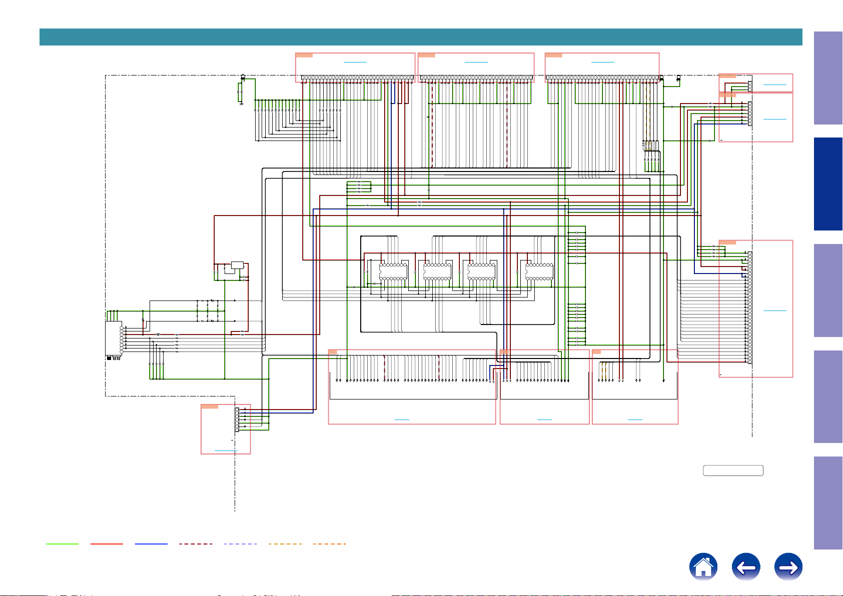
SCH20_AUDIO/VIDEO CONNECT
R3128
C3134
1K
10/63
100K
R3130
100K
R3126
100K
100K
R3127
0
33
33
33
33
2.2K
R3131
R3129
C3135
1K
10/63
N9015
To_8U-210228-8(N9016)
11
9
10
12
CG
CG
CG
CG
1
LOUT
2
ROUT
3
VCC
4
SCLK
5
SDIO
6
/SEN
7
/RST
8
GPIO2/INT
Z3001
TUNER_MODULE
C7716
TUNER_L
TUNER_R
TU+5V
TU_SCLK
TU_SDIO
TU_SEN
TU_RST
TU_GPIO2
OPEN
BLM21PG221
100P
100P
C3123
C3126
L3003
100P
C3127
100P
100P
C3129
C3128
R8072
R3134
R3135
R3136
R3137
R3138
1u
0.1
10K
R8213
C7712
C7714
82K
R3132
82K
R3133
A+7V
A-7V
PREGND
PHONOL
PREGND
PHONOR
PREGND
CONNECT-4_UNIT
TO N9016
B3001
M3-SIDE
OPEN
OPEN
C3029
C3027
PREGND
U7524
PQ050DNA1ZPH
3
VOUT
1
VIN
NC
4
ON/OFF
GND
2
5
C7713
4.7u
C7715
0.1
TUNERR
TUNERL
R8214
0
R8215
OPEN
1
2
3
PHONOL
4
5
PHONOR
6
7
N9015
7P-SOCKET(C125Z2)
1M
0.1
R3009
C3001
TUSCL
TUSDA
TUSEN
TURST
TUGPIO
1M
0.1
R30101MR3011
C3002
0.1
0.1
0.1
0.1
1M
0.1
C3006
C3007
C3005
C30041MR3015
R3013
C30031MR30121MR3014
AEXPDATA
AEXP_OE
AEXP_STB
AEXP_CLK
N9019
N9019
33P-SOCKET(C125Z2)
33
DGND
M3.3V
DA3.3V
AMPSIGDET
AMPSIGDET
CURRENTDET
CURRENTDET
TEHRMALE
THERMALF
100
100
R3017
R3016
THERMALDET_F
THERMALDET_E
All Ref.No. has been described in the parts list are four digits.
But there are less than four digits of printed Ref.No. on the PCB, and they have become four digits after the header by adding "0" in the parts list.
123456789
DAZ3L
DAZ2R
DAZ3R
DACGND
DA_Z2R
DA_Z3L
DA_Z3R
RLYGND
SPRL_RSV3
SPRL_RSV2
SPRL_RSV1
11Q812Q713Q614Q515OE16
VDD
STB2DATA3CLK4Q15Q26Q37Q48VSS
OPEN
1
U3004
PRERL_S
PRERL_F
PRERL_C
PRERL_SB
PRERL_Z3
PRERL_H2
PRERL_SW2
PRERL_SW1
PRERL_C
PRERL_F
PRERL_S
PRERL_H1
PRERL_Z3
PRERL_SB
PRERL_H2
PRERL_SW1
PRERL_SW2
TO PREOUT
TO 6H
N9018
N9018
33P-FFC
33
H/PR
H/PL
H/PGND
H/PL
H/PR
9
10
QS
Q'S
H/PR
H/PRL
PRERL_Z2
H/PRL
PRERL_Z2
H/PGND
H/PL
H/PL
H/PR
MIC
PREGND
MICIN
H/PGND
VAUXR
VAUXR
RLYGND
DGND
VAUXL
VAUXL
C5575
C5571
C5572
C5573
C5574
C5576
C3044
C3038
C3039
C3040
C3041
C3042
C3043
C3045
C3046
C3047
C3048
C3049
PREGND
TO N6010
DGND
ZVOLSTB
VOL_CLK
SEL_CLK
ZVOLCLK
ZVOLDATA
SEL_DATA
VOL_DATA
ZVOLDA
ZVOLCLK
ZVOLST
SEL_CLK
SEL_DATA
VOL_CLK
VOL_DATA
1000P
1000P
1000P
1000P
1000P
1000P
1000P
1000P
1000P
1000P
1000P
1000P
1000P
1000P
1000P
1000P
1000P
1000P
H7
VAUX_V
DECIN_V
VAUX_V
TO ANALOG VIDEO
To_8U-310223(N6010)
AEXP_STB
AEXP_CLK
AEXP_CLK
AEXP_STB
DECIN_Y
DECIN_CB
DECIN_Y
DECIN_V
AEXP_OE
AEXPDATA
AEXPDATA
AEXP_OE
DECIN_CR
DECIN_CR
DECIN_CB
DV5V
DV3.3V
DV+5V
DGND
DV+3.3V
DIGITALUNIT(1/19)
1011121314151617181920212223242526272829303132
DGND
AVSDA
AVSDA
DGND
AVSCL
C3026
AVSCL
AVSDA
AVSCL
AVSDA
AVSCL
AUX_V
DECIN_Y
DECIN_V
DECIN_Cb
DECIN_CB
DECIN_V
DECIN_Y
10/6.3
VAUX_V
OPEN
OPEN
OPEN
R3036
R3035
R303075R3037
B3002
123456789
M3-SIDE
DECIN_Cr
C3010
DECIN_CR
OPEN
R3038
DGND
1000P
B3003
M3-SIDE
ASODET
DCDET
TRDET
AMPSIGDET
SPRL_H2
SPRL_H3
SPRL_H1
SPRL_RSV3
SPRL_RSV2
SPRL_RSV1
SPRL_SB
SPRL_S
SPRL_C
SPRL_F
FANCONT_LOW
FANCONT_HIGH
FANCONT_MID
FANCONT_NC
BRL_HIGH
FANDET_HIGH
FANDET_ON
THERMALDET_F
THERMALDET_E
CURRENTDET
M3.3V
TO 7H
8U-210228-1(1/4)
A.AUDIO/VIDEO_UNIT
OPEN
R8211
R8212
OPEN
C3008
1000P
0
R3027
0
R3028
0
R3033
0
R3034
To_8U-110210-1(N6013)
SPEAKER_UNIT(1/2)
To_8U-210228-2(N9001)
DAC_UNIT(2/2)
N9035
N9035
3P-SAN
N9028
To_8U-110210-1(N6204)
SPEAKER_UNIT(2/2)
N3003
PREPOWERGND
PREPOWERGND
DGND
DGND
A+7V
A+7V
A-7V
A-7V
ASODET
DCDET
TRDET
AMPSIGDET
SPRL_H2
SPRL_H3
SPRL_H1
SPRL_RSV3
SPRL_RSV2
SPRL_RSV1
SPRL_SB
SPRL_S
SPRL_C
SPRL_F
FANCONT_LOW
FANCONT_HIGH
FANCONT_MID
NC
BRL_HIGH
FANDET_HIGH
FANDET_ON
TEHRMALDET_F
THERMALDET_E
CURRENTDET
M3.3V
TRDET
FANDET_ON
100
100
R3018
R3020
FANDET_ON
TRDET
M3.3V
H5
DCDET
FANDET_HIGH
100
100
R3019
R3021
DCDET
FANDET_HIGH
PHONOL
TO N5910
DGND
TUGPIO
ASODET
100
R3022
ASODET
TUGPIO
PHONOR
PHONOL
PHONOR
TUSEN
TURST
TURST
TUSEN
R3001
R3002
R3003
R3004
C3022
0.1
TUNERR
TUNERL
PREGND
TUNERL
TUSDA
TUSDA
R8158
VAUXL
VAUXL
TUNERR
TUSCL
TUSCL
VAUXR
VAUXR
DGND
0
0
0
0
0.1
C3023
MICIN
MICIN
AEXP_CLK
AEXP_CLK
4.7K
R3026
DA_Z3L
DA_Z3L
N3001
To_8U-210228-6_(N5910)
CONNECT-1_UNIT
1011121314151617181920212223242526272829303132
DGND
A-7V
AEXP_OE
TRIG12V
TRIGGND
AEXPDATA
AEXP_STB
TRIG12V
TRIGGND
AEXPDATA
AEXP_STB
AEXP_OE
OPEN
PRERL_C
PRERL_SW1
16
Q515OE
VDD
U3001
STB2DATA3CLK4Q15Q26Q37Q48VSS
CD74HC4094PWR
1
C3037
OPEN
PRERL_H1
DA_SL
DA_FL
DA_FR
DA_Z3R
DA_Z2R
DA_Z2L
DA_FL
DA_FR
DA_Z3R
DA_Z2R
DA_Z2L
TO AUDIO VOLUME
N3001
33P-SOCKET(C125Z2)
123456789
33
A+7V
A-7V
A+7V
PRERL_F
PRERL_S
11Q812Q713Q614
PRERL_SB
PRERL_SW2
PRERL_H2
DA_C
DA_SR
DA_C
DA_SL
DA_SR
TO 8U-210228-1(2/4) TO 8U-210228-1(3/4) TO 8U-210228-1(4/4)
TO 5H
10
Q'S
DA+5V
9
QS
DA_SW1
DA_SW1
DA+5V
DA_SW2
VOLMUTE
VOLMUTE
R8159
R8157
0.1
C3024
DA_SBR
DA_SBL
DA_SW2
DA_SBL
DA_H1L
DA_SBR
NETL
NETL
0
0
U3002
DA_H1R
DA_H1L
DAFL
NETR
DACGND
NETR
DA_FL
1000P
C3009
SPRL_C
VDD
STB2DATA3CLK4Q15Q26Q37Q48VSS
CD74HC4094PWR
1
DA_H2L
DA_H3L
DA_H2R
DA_H2L
DA_H3L
DA_H2R
DA_H1R
DAC
DAFR
DACGND
DA_FR
DA_C
SPRL_F
SPRL_S
SPRL_SB
PRERL_Z3
PRERL_Z2
H/PRL
ADINL.
DA_H3R
ADINR.
ADINL.
DA_H3R
DASW1
A_SW1
D
11Q812Q713Q614Q515OE16
ZADINL.
ADINR.
DASW2
DA_SW2
9
10
QS
Q'S
ZADINR.
ZADINR.
ZADINL.
DACGND
NETL
DASL
DA_SL
NETR
NETL
NETR
TO N5904
DASR
DASBL
DACGND
DA_SR
DA_SBL
0.1
C3028
U3003
VOLMUTE
VOL_DATA
VOLMUTE
DAH2R
DAH1R
DAH2L
DAH3L
DASBR
DAH1L
DAH3R
DACGND
DA_H3R
DA_H3L
DA_H1L
DA_H1R
DA_H2R
DA_H2L
DA_SBR
SPRL_H1
SPRL_H2
SPRL_H3
BRL_HIGH
10
11Q812Q713Q614Q515OE16
Q'S
VDD
STB2DATA3CLK4Q15Q26Q37Q48VSS
CD74HC4094PWR
1
FANCONT_MID
FANCONT_LOW
FANCONT_NC
FANCONT_HIGH
ZVOLST
ZVOLDA
SEL_CLK
VOL_CLK
ZVOLCLK
SEL_DATA
A-7V
ZVOLDA
ZVOLST
SEL_CLK
VOL_CLK
ZVOLCLK
SEL_DATA
VOL_DATA
To_8U-210228-7(N5904)
CONNECT-2_UNIT
1011121314151617181920212223242526272829303132
ADINR
ADINL
ZADINR
DACGND
ZADINL
DACGND
ZADINL.
ZADINR.
ADINR.
ADINL.
9
QS
H6
A-7V
A+7V
A+7V
RLY+13V
DAZ2L
DA_Z2L
OPEN
C3025
PRERL_H1
AUDIO/VIDEO CONNECT
Condential
N9028
7P-PH
33
32
31
30
29
28
27
26
25
24
23
22
21
20
19
18
17
16
15
14
13
12
11
10
1
2
3
1
2
3
4
5
6
7
9
8
7
6
5
4
3
2
1
DA+5V
DAGND
RLYB+13V
RLYGND
A+7V
PREGND
A-7V
N3003
TO N9001
TO N6204
TO N6013
33P-FFC
Caution in
servicing
Electrical Mechanical Repair Information Updating
GND LINE
POWER+ LINE
POWER- LINE
AUDIO SIGNAL
TMDS SIGNAL
ANALOG VIDEO
DIGITAL VIDEO
29
Page 30
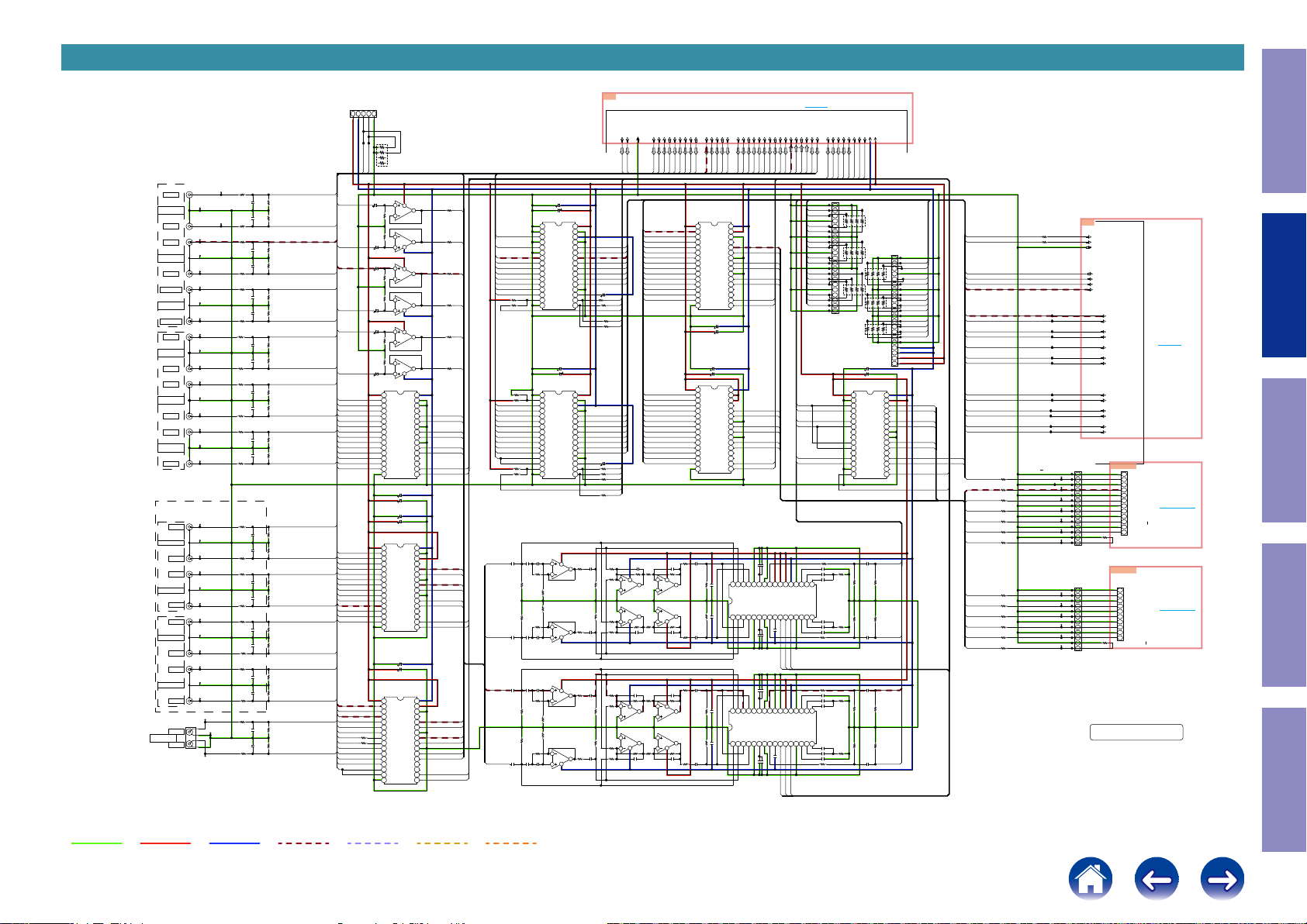
SCH21_AUDIO VOLUME
6
BDL
5
INPUT
1
BDR
2
7
DVDL
INPUT
DVDR
3
8
CBL/SATL
INPUT
UP
RCA-637-00-04
CBL/SATR
4
K3102
8
GAMEL
INPUT
GAMER
4
7
MPL
INPUT
MPR
3
6
CDL
5
INPUT
K3103
1
CDR
2
RCA-637-00-04
AVR-X6400H:OPEN
8
EXT.FL
FRONT
UP
EXTFR
4
7
EXTSL
SURR.
MID
K3104
EXTSR
3
RCA-637-00-04
8
EXTSBL
S.BACK
UP
EXTSBR
4
7
EXTSW
C/SW
MID
EXTC
3
K3105
RCA-637-00-04
TUMERR
INPUT
TUNERL
1 2 3 4
K3106
OPEN
R3201
470
R3202
470
R3203
470
R3204
470
R3205
470
R3206
470
R3207
470
R3208
470
R3209
470
R3210
470
R3211
470
R3212
470
R3215
OPEN
R3216
OPEN
R3217
OPEN
R3218
OPEN
R3219
OPEN
R3220
OPEN
R3221
OPEN
R3222
OPEN
R3213
OPEN
R3214
OPEN
C3201
330P
C3202
330P
C3203
330P
C3204
330P
C3205
330P
C3206
330P
C3207
330P
C3208
330P
C3209
330P
C3210
330P
C3211
330P
C3212
330P
C3215
OPEN
C3216
OPEN
C3217
OPEN
C3218
OPEN
C3219
OPEN
C3220
OPEN
C3221
OPEN
C3222
OPEN
C3213
OPEN
C3214
OPEN
R3223
820K
R3224
820K
R3225
820K
R3226
820K
R3227
820K
R3228
820K
R3229
820K
R3230
820K
R3231
820K
R3232
820K
R3233
820K
R3234
820K
R3237
820K
R3238
820K
R3239
820K
R3240
820K
R3241
820K
R3242
820K
R3243
820K
R3244
820K
R3247
OPEN
R3248
OPEN
CBL/SATL
CBL/SATR
EXT_FL
EXT_FR
EXT_SL
EXT_SR
EXT_SBL
EXT_SBR
EXT_SW
BDL
BDR
DVDL
DVDR
GAMEL
GAMER
MPL
MPR
CDL
CDR
EXT_C
TUNERR
TUNERL
ADINL
ADINR
ZADINL
ZADINR
Z3LLINE
Z3RLINE
GAMEL
GAMER
MPL
MPR
DA_Z2L
DA_Z2R
DA_Z3L
DA_Z3R
CDL
CDR
VAUXL
VAUXR
NETL
NETR
TUNERL
TUNERR
PHONOL
PHONOR
DA_FL
DA_FR
CBL/SATL
CBL/SATR
XLRL
XLRR
DVDL
DVDR
BDL
BDR
MAININL
MAININR
DA_FL
DA_FR
EXT_FL
EXT_FR
EXT_FL
EXT_C
NETL
NETR
ZADINL.
ZADINR.
MICIN
A+7V
R3236
R3365
All Ref.No. has been described in the parts list are four digits.
But there are less than four digits of printed Ref.No. on the PCB, and they have become four digits after the header by adding "0" in the parts list.
Caution in
5H
2
345
1
OPEN
N3209
7 8
5 6
XLRL
A-7V
XLRR
AGND
3 4
R3374
1 2
47Kx4
XLRR
XLRL
C7652
U7520
OPEN
10/63
NJM8080G
3
8
R8084
47
1
U7520
NJM8080G
7
U7521
NJM8080G
1
U7521
NJM8080G
7
U7523
NJM8080G
1
U7523
NJM8080G
7
V-
32
ADR1
31
ADR0
30
NC
29
28
27
26
25
24
23
22
21
NC
20
NC
19
18
DATA
17
100/16
100/16
100/16
100/16
V-
32
ADR1
31
ADR0
30
NC
29
28
27
26
25
24
23
22
21
NC
20
NC
19
18
DATA
17
100/16
100/16
V-
32
ADR1
31
ADR0
30
NC
29
28
27
26
25
24
23
22
21
NC
20
NC
19
18
DATA
17
R8085
R8086
R8087
R8088
R8089
ADINL.
ADINR.
47
ZADINL.
ZADINR.
Z3LLINE.
Z3RLINE.
MAININL
MAININR
ZADINL
ZADINR
Z3LLINE
Z3RLINE
SEL_CLK
SEL_DATA
MAININL
MAININR
ZADINL
ZADINR
Z3LLINE
Z3RLINE
SEL_CLK
SEL_DATA
ADINL
ADINR
Z2LLINE.
Z2RLINE.
SEL_CLK
SEL_DATA
EXT_C
47
DA_C
FL
FR
DA_H1L
DA_H1R
DA_SL
DA_SR
EXT_SL
EXT_SR
47
47
47
R3282
R3283
EXT_SBL
EXT_SBR
DA_SBL
DA_SBR
DA_H2L
DA_H2R
DA_H3L
DA_H3R
DA_SW1
DA_SW2
EXT_SW
Z3LLINE.
Z3RLINE.
Z2LLINE.
FL
FR
Z2RLINE.
2
470K
R8080
470K
6
R8081
C7653
10/63
4
5
C7654
10/63
3
8
2
470K
R8082
470K
R8083
6
C7655
10/63
4
5
C7656
10/63
3
8
2
470K
R8090
470K
R8091
6
C7657
10/63
4
5
U3212
NJU72750V
V+
1
InA1
2
InB1
3
InA2
4
OutA1
InB2
5
OutB1
InA3
6
REF_A
InB3
7
OutA2
InA4
8
OutB2
InB4
9
REF_B
InA5
10
OutA3
InB5
11
OutB3
InA6
12
InB6
13
InA7
14
CLOCK
InB7
15
REF
16
C3252
C3245
C3255
C3254
U3213
NJU72750V
V+
1
InA1
2
InB1
3
InA2
4
OutA1
InB2
5
OutB1
InA3
6
REF_A
InB3
7
OutA2
InA4
8
OutB2
InB4
9
REF_B
InA5
10
OutA3
InB5
11
OutB3
InA6
12
InB6
13
InA7
14
CLOCK
InB7
15
REF
16
C3251
C3241
U3214
NJU72750V
1
V+
2
InA1
3
InB1
4
InA2
OutA1
5
InB2
OutB1
6
InA3
REF_A
7
InB3
OutA2
8
InA4
0
OutB2
9
InB4
REF_B
InA5
10
OutA3
InB5
11
OutB3
InA6
12
InB6
13
InA7
14
CLOCK
InB7
15
REF
16
R3287
R8167
R3286
R8166
C3301
10/16
C3302
10/16
C3303
10/16
C3304
10/16
OPEN
0
0
470K
OPEN
OPEN
0
C3305
0.01
470K
R3301
R3302
C3306
0.01
C3307
0.01
470K
R3303
470K
R3304
C3308
0.01
C3309
0.01
R3305
150K
R3306
150K
C3310
0.01
C3311
0.01
R3307
150K
R3308
150K
C3312
0.01
C3260
C3242
U3215
NJU72343V
Z/C_REF
1
ADR
2
InA2
3
InB2
4
InA1
5
InB1
6
InC
7
InD
8
InE
9
InF
10
InG1
11
InH1
12
InG2
13
VDDOUT
InH2
14
CLOCK
MUTE
15
REF
16
C3250
C3259
U3216
NJU72343V
1
Z/C_REF
2
ADR
3
InA2
4
InB2
5
InA1
6
InB1
7
InC
8
InD
9
InE
InF
10
InG1
11
InH1
12
InG2
13
VDDOUT
InH2
14
CLOCK
MUTE
15
REF
16
3
8
1/2
2
U3205
NJM8080G
R3309
330K
R3310
330K
NJM8080G
U3205
6
2/2
4
5
3
8
1/2
2
U3206
NJM8080G
R3311
330K
R3312
330K
NJM8080G
U3206
6
2/2
4
5
220/25
220/25
V+
AREF
VAREF
OutA
OutB
OutC
OutD
OutE
OutF
OutG
OutH
AREF
DATA
220/25
220/25
V+
AREF
VAREF
OutA
OutB
OutC
OutD
OutE
OutF
OutG
OutH
AREF
DATA
1
7
1
7
32
31
30
29
28
27
26
25
24
23
22
21
20
19
18
17
32
31
30
29
28
27
26
25
24
23
22
21
20
19
18
17
R3313
100
R3314
100
R3315
100
R3316
100
R8173
R8172
C3313
10/16
R3317
100K
R3318
100K
C3314
10/16
C3315
10/16
R3319
100K
R3320
100K
C3316
10/16
OPEN
R8169
OPEN
R8170
R8171
R3280
R8168
R3281
PREOUT_C
PREOUT_RSV
PREOUT_FL
PREOUT_FR
PREOUT_H1L
PREOUT_H1R
PREOUT_SL
PREOUT_SR
C3258
1/50
SEL_CLK
SEL_DATA
VOLMUTE
0
VOL_CLK
VOL_DATA
0
PREOUT_SBL
PREOUT_SBR
PREOUT_H2L
PREOUT_H2R
PREOUT_H3L
PREOUT_H3R
PREOUT_SW1
PREOUT_SW2
C3257
1/50
VOL_CLK
0
SEL_DATA
SEL_CLK
VOLMUTE
0
VOL_DATA
R3321
39K
R3323
39K
R3324
39K
R3322
39K
R3325
39K
R3327
39K
R3328
39K
R3326
39K
PREGND-VAUXL
PHONOR-TUNERL
PHONOL
-
PHONOL
PHONOR
OPEN
OPEN
C3317
100P
R3329
2
4
22K
1/2
1
3
U3207
NJM8080G
U3208
NJM8080G
3
1/2
1
22K
4
2
R3330
C3318
100P
C3319
100P
R3331
2
4
22K
1/2
1
3
U3209
NJM8080G
U3210
NJM8080G
3
1/2
1
22K
4
2
R3332
C3320
100P
TUNERR
-
VAUXL
TUNERL
TUNERR
.PREOUT_FL
.PREOUT_FR
.PREOUT_SL
.PREOUT_SR
.PREOUT_C
PREOUT_RSV
.PREOUT_SBL
.PREOUT_SBR
.PREOUT_H1L
.PREOUT_H1R
.PREOUT_H2L
.PREOUT_H2R
PREOUT_H3L
PREOUT_H3R
.PREOUT_FL
.PREOUT_FR
.PREOUT_SL
.PREOUT_SR
.PREOUT_C
PREOUT_RSV
.PREOUT_SBL
.PREOUT_SBR
.PREOUT_H1L
.PREOUT_H1R
.PREOUT_H2L
.PREOUT_H2R
PREOUT_H3L
PREOUT_H3R
R3333
4.7K
6
2/2
5
5
2/2
6
R3334
4.7K
R3335
4.7K
6
2/2
5
5
2/2
6
R3336
4.7K
MICIN
VAUXR
DA_Z3L
-
-
-
DA_Z3L
VAUXR
MICIN
C3321
R3341
100P
47
R3337
8
4.7K
7
U3207
NJM8080G
U3208
NJM8080G
7
4.7K
8
R3338
R3342
47
C3322
100P
C3323
100P
R3343
R3339
8
4.7K
7
U3209
NJM8080G
U3210
NJM8080G
7
4.7K
8
R3340
R3344
47
C3324
100P
TO AUDIO/VIDEO CONNECT
DA_C
DA_SW2
DA_SL
DA_SBR
DA_SW1
DA_SBL
DA_SR-DA_FR
DA_FL
DA_Z3R
DA_Z2R-DA_Z2L
-
-
-
-
-
-
-
-
-
-
-
DA_Z3R
47
DA_Z2L
C3325
10/16
C3326
10/16
C3327
10/16
C3328
10/16
DA_Z2R
C3253
C3256
DA_FR
DA_SL
DA_FL
U3217
NJU72750V
V+
1
InA1
2
InB1
3
InA2
4
InB2
5
InA3
6
InB3
7
InA4
8
InB4
9
InA5
10
InB5
11
InA6
12
InB6
13
InA7
14
InB7
15
REF
16
C3244
C3243
U3218
NJU72750V
1
V+
2
InA1
3
InB1
4
InA2
5
InB2
6
InA3
7
InB3
8
InA4
9
InB4
InA5
10
InB5
11
InA6
12
InB6
13
InA7
14
InB7
15
REF
16
100K
0.1
C3329
R3345
100K
0.1
R3346
C3330
0.1
100K
R3347
C3331
0.1
100K
C3332
R3348
DA_SR
VADR1
ADR0
NC
OutA1
OutB1
REF_A
OutA2
OutB2
REF_B
OutA3
OutB3
NC
NC
CLOCK
DATA
100/16
100/16
100/16
100/16
VADR1
ADR0
NC
OutA1
OutB1
REF_A
OutA2
OutB2
REF_B
OutA3
OutB3
NC
NC
CLOCK
DATA
DA_C
32
31
30
29
28
27
26
25
24
23
22
21
20
19
18
17
32
31
30
29
28
27
26
25
24
23
22
21
20
19
18
17
32
1
32
1
DA_SW2
DA_SBL
DA_SW1
INB131INB230INB329INB4
U3203
INA1
INA23INA34INA45GND
2
INB131INB230INB329INB4
U3204
INA1
INA23INA34INA45GND
2
DA_SBR
AMPIN_FL
AMPIN_FR
AMPIN_SL
AMPIN_SR
AMPIN_H3L
AMPIN_H3R
VOL_DATA
AMPIN_SBL
AMPIN_SBR
AMPIN_H1L
AMPIN_H1R
AMPIN_H2L
AMPIN_H2R
VOL_DATA
C3333
28
27
GND
C3334
C3335
28
27
GND
C3336
ADINL.
DA_H1L
DA_H1R
DA_H2L
DA_H2R
DA_H3L
DA_H3R
-
-
-
---
-
ADINL.
DA_H1L
DA_H2L
DA_H2R
DA_H1R
DA_H3L
DA_H3R
VOL_CLK
VOL_CLK
C3337
OPEN
10/16
26
25
22
GND
VCC21VDD20GND
OUTB24ADR123ADR0
NJW1194
DCCAP_B
GND
DCCAP_A
OUTA9VDDOUT10DATA11CLOCK12LATCH13GND14TREA15BASSA116BASSA2
6
7
8
C3341
10/16
OPEN
10/16
C3338
ZVOLCLK
ZVOLDA
10/16
OPEN
C3339
26
25
22
GND
VCC21VDD20GND
OUTB24ADR123ADR0
NJW1194
DCCAP_B
GND
DCCAP_A
OUTA9VDDOUT10DATA11CLOCK12LATCH13GND14TREA15BASSA116BASSA2
6
7
8
10/16
C3342
OPEN
C3340
10/16
ZVOLST ZVOLST
ZVOLCLK
ZVOLDA
TO H5
ZADINR.
ZADINL.
ADINR.
-
-
-
ADINR.
ZADINL.
ZADINR.
PREOUT_SBR
PREOUT_SBL
.PREOUT_SBL
.PREOUT_SBR
PREOUT_FR
PREOUT_FL
.PREOUT_FL
.PREOUT_FR
PREOUT_C
PREOUT_SR
PREOUT_SL
.PREOUT_SL
.PREOUT_SR.PREOUT_SR
.PREOUT_C
.PREOUT_FL
.PREOUT_FR
19
18
TREB
BASSB117BASSB2
C3360
C3344
R3350
19
18
TREB
BASSB117BASSB2
C3362
C3346
R3352
NETL
NETR
-
-
NETR
NETL
PREOUT_Z2L
PREOUT_Z2R
PREOUT_Z3L
PREOUT_Z3R
R3349
C3343
C3359
C3347
10/16
C3348
10/16
R3351
C3345
C3361
C3349
10/16
C3350
10/16
VOLMUTE
100
3300P
0.1
0.1
3300P
100
100
3300P
0.1
0.1
3300P
100
TO 8U-210228-1(1/4)
ZVOLDA
ZVOLCLK
VOL_CLK
VOLMUTE
SEL_DATA
SEL_CLK
VOL_DATA
-
-
-
-
-
ZVOLCLK
ZVOLDA
SEL_DATA
SEL_CLK
VOL_CLK
VOL_DATA
N9033
OPEN
1
2
3
123456
78
4
5
6
7
8
9
123456
78
10
11
12
13
14
15
16
123456
78
17
18
19
0x4
R3381
20
21
R3382
R3384
C3248
C3249
NJU72751V
V+
1
ADR0
2
InA1
3
InB1
4
NC
5
InA2
6
InB2
7
NC
8
NC
9
InA3
10
InB3
11
NC
12
InA4
13
InB4
14
REF
15
DATA
16
C3355
10/16
100K
R3353
4.7K
R3357
100K
R3354
4.7K
C3356
R3358
10/16
C3357
10/16
100K
4.7K
R3355
R3359
100K
R3356
4.7K
C3358
R3360
10/16
A-7V
ZVOLST
ZVOLST
0x4
R3378
0x4
R3379
0x4
R3380
123456
123456
0x4
123456
0x4
100/16
100/16
U3219
ADR1
OutA1
OutB1
OutA2
OutB2
REF_A
REF_B
OutA3
OutB3
OutA4
OutB4
CLOCK
A+7V
N9034
OPEN
1
2
3
78
4
5
6
7
8
78
9
10
11
12
13
78
14
15
16
17
18
19
20
21
V-
32
31
30
29
NC
28
27
26
25
24
23
22
NC
21
20
19
NC
18
17
PREOUT_Z3L
R3361
100K
R3362
100K
PREOUT_Z3R
PREOUT_Z2L
R3363
100K
R3364
100K
PREOUT_Z2R
PREOUT_SW1
PREOUT_SW2
.PREOUT_SW2
.PREOUT_SW1
PREOUT_H1R
PREOUT_H1L
.PREOUT_H1L
.PREOUT_H1R.PREOUT_H1R
PREOUT_H2R
PREOUT_H2L
.PREOUT_H2L
.PREOUT_H2R.PREOUT_H2R
AMPIN_SBL
AMPIN_SBR
AMPIN_H1L
AMPIN_H1R
AMPIN_H2L
AMPIN_H2R
VOL_CLK
VOL_DATA
.
47
47
.PREOUT_H1L
.PREOUT_H2L
.PREOUT_H2R
14
13
12
11
10
9
8
7
6
5
4
3
2
1
N3204
OPEN
N3201
OPEN
1
2
3
4
5
6
7
8
9
10
11
12
H8
.H/PIN_FL
.H/PIN_FR
PREOUT_Z3R
PREOUT_Z3L
PREOUT_Z2R
PREOUT_Z2L
.PREOUT_FL
.PREOUT_FR
.PREOUT_SL
.PREOUT_SR
.PREOUT_C
.PREOUT_SW1
.PREOUT_SW2
.PREOUT_SBL
.PREOUT_SBR
.PREOUT_H1L
.PREOUT_H1R
.PREOUT_H2L
.PREOUT_H2R
.H/PIN_FL
.H/PIN_FR
.PREOUT_C
AMPIN_FL
AMPIN_SL
AMPIN_SBL
AMPIN_H1L
AMPIN_H2L
AMPIN_H3L
AMPIN_FR
AMPIN_SR
AMPIN_SBR
AMPIN_H1R
AMPIN_H2R
AMPIN_H3R
8U-210228-1(2/4)
A.AUDIO/VIDEO_UNIT
R3277
R3278
R3279
R3288
R3289
R3290
R3291
R3292
R3293
R3294
R3295
R3296
R3297
47
47
47
47
47
47
OPEN
47
47
47
47
47
OPEN
INGND
INGND
INGND
INGND
INGND
INGND
INGND
INGND
INGND
INGND
INGND
INGND
INGND
R3245
R3246
AUDIO VOLUME
H/PIN_FL
H/PIN_FR
PREGND
PREOUT_Z3R
PREOUT_Z3L
PREOUT_Z2R
PREOUT_Z2L
.PREOUT_FL
.PREOUT_FR
.PREOUT_SL
.PREOUT_SR
.PREOUT_C
.PREOUT_SW1
.PREOUT_SW2
.PREOUT_SBL
.PREOUT_SBR
.PREOUT_H1L
.PREOUT_H1R
.PREOUT_H2L
.PREOUT_H2R
N3206
GND
12
C
11
GND
10
FL
9
GND
8
SL
7
GND
6
SBL
5
GND
4
H2L
3
GND
2
H3L
1
R8199
GND
0
N3206
H1L
12P-PH
N9204
N9024
10P-PH
GND
1
FR
2
GND
3
SR
4
GND
5
SBR
6
GND
7
H2R
8
GND
9
H3R
10
R8198
GND
0
H1R
Condential
TO 8H
TO 8U-210228-1(3/4)
TO N5833
L_AMP_CONNECT_UNIT
To_8U-210228-3(N5833)
TO N5821
R_AMP_CONNECT_UNIT
To_8U-210228-4(N5821)
servicing
Electrical Mechanical Repair Information Updating
GND LINE
POWER+ LINE
POWER- LINE
AUDIO SIGNAL
TMDS SIGNAL
ANALOG VIDEO
DIGITAL VIDEO
30
Page 31

SCH22_PREOUT
8H
TO VOLUME
TO 8U-210228-1(2/4)
TO H8
-
G6J-2P-Y
KDS160
1
8
D3501
S3501
-
0
R3501
Q3501
Q3503
KRC105S
KRC105S
6H
TO AUDIO/VIDEO CONNECT
H/PIN_FL
H/PIN_FR
PREGND
PREOUT_Z3R
PREOUT_Z3L
PREOUT_Z2R
PREOUT_Z2L
.PREOUT_FL
.PREOUT_FR
.PREOUT_SL
.PREOUT_SR
.PREOUT_C
.PREOUT_SW1
.PREOUT_SW2
.PREOUT_SBL
.PREOUT_SBR
.PREOUT_H1L
.PREOUT_H1R
.PREOUT_H2L
.PREOUT_H2R
-
-
G6J-2P-Y
G6J-2P-Y
KDS160
KDS160
1
1
8
8
D3503
D3502
S3502
S3503
-
-
0
0
R3502
R3503
Q3505
Q3507
KRC105S
KRC105S
RLY+13V
PRERL_H1
A-7V
A+7V
PRERL_H1
PRERL_H2
H/PIN_FL
H/PIN_FR
PREOUT_Z3R
PREOUT_Z3L
PREOUT_Z2R
PREOUT_Z2L
.PREOUT_FL
.PREOUT_FR
.PREOUT_SL
.PREOUT_SR
.PREOUT_C
.PREOUT_SW1
.PREOUT_SW2
.PREOUT_SBL
.PREOUT_SBR
.PREOUT_H1L
.PREOUT_H1R
.PREOUT_H2L
.PREOUT_H2R
-
G6J-2P-Y
KDS160
1
8
D3504
S3504
-
0
R3504
Q3509
KRC105S
TO 8U-210228-1(1/4)
PRERL_H2
PRERL_Z3
PRERL_SW2
PRERL_SB
PRERL_C
PRERL_F
PRERL_S
PRERL_SW1
PRERL_SW2
PRERL_SB
PRERL_Z2
PRERL_SW1
PRERL_C
PRERL_Z3
PRERL_F
PRERL_S
-
-
G6J-2P-Y
G6J-2P-Y
KDS160
KDS160
1
1
8
8
D3506
D3505
S3506
S3505
-
-
0
0
R3506
R3505
Q3511
Q3513
KRC105S
KRC105S
TO H6
H/PR
H/PL
PRERL_Z2
H/PRL
RLY+13V
-
KDS160
D3507
-
Q3515
KRC105S
RLYGND
H/PGND
G6J-2P-Y
1
8
S3507
0
R3507
PREGND
-
KDS160
1
8
D3508
S3508
-
0
R3508
Q3517
KRC105S
All Ref.No. has been described in the parts list are four digits.
But there are less than four digits of printed Ref.No. on the PCB, and they have become four digits after the header by adding "0" in the parts list.
Caution in
servicing
U3501
C3538
OPEN
OPEN
OPEN
OPEN
OPEN
OPEN
OPEN
OPEN
OPEN
OPEN
OPEN
OPEN
OPEN
OPEN
OPEN
OPEN
OPEN
R3526
220K
R3527
220K
C3536
10/63
R3528
220K
R3529
C3537
10/63
220K
220P
R3531
C3539
220P
3
[2/2]
2
R3530
1K
1K
6
[1/2]
5
8
4
H/PIN_FR
H/PIN_FL
C3519
10/63
PREOUT_Z3R
R8174
R8175
C3520
10/63
PREOUT_Z3L
C3521
PREOUT_Z2R
10/63
.PREOUT_FR
.PREOUT_FL
.PREOUT_SR
.PREOUT_SL
.PREOUT_SBR
.PREOUT_SBL
.PREOUT_C
.PREOUT_SW1
.PREOUT_SW2
.PREOUT_H1R
.PREOUT_H1L
.PREOUT_H2R
.PREOUT_H2L
G6J-2P-Y
1
8
S3512
0
PREOUT_Z2L
R8176
R8177
R8178
R8179
R8180
R8181
R8182
R8183
R8184
R8185
R8186
R8189
R8190
R8191
R8192
C3522
10/63
C3523
10/63
C3524
10/63
C3525
10/63
C3526
10/63
C3530
10/63
C3531
10/63
C3527
10/63
C3528
10/63
C3529
10/63
C3534
10/63
C3535
10/63
C3559
10/63
C3560
10/63
H/PGND
R3031
0
0
R3032
-
-
G6J-2P-Y
KDS160
D3509
S3509
-
0
R3574
-
Q3521
KRC105S
KDS160
1
8
D3511
S3511
-
0
R3586
Q3523
KRC105S
G6J-2P-Y
KDS160
D3512
-
R3587
G6J-2P-Y
1
8
NJM4556AD
1
C3540
220/25
R3532
2.2K
R3533
2.2K
7
C3541
220/25
U3501
NJM4556AD
R3509
100K
R3510
100K
R3511
100K
R3512
100K
R3513
100K
R3514
100K
R3515
100K
R3516
100K
R3520
100K
R3521
100K
R3517
100K
R3518
100K
R3519
100K
R3524
100K
R3525
100K
R3575
100K
R3576
100K
R3577
R3578
R3534
R3579
R3535
R3580
S3506
G6J-2P-Y
S3507
G6J-2P-Y
S3508
G6J-2P-Y
5 7
4 2
5 7
4 2
5 7
4 2
5 7
4 2
5 7
4 2
4
4
4
5 7
4 2
5 7
4 2
100
100
100
2.2K
R3536
2.2K
100
100
R3537
100
6
S3502
G6J-2P-Y
S3502
G6J-2P-Y
3
6
S3503
G6J-2P-Y
S3503
G6J-2P-Y
3
6
S3504
G6J-2P-Y
S3504
G6J-2P-Y
3
6
S3505
G6J-2P-Y
S3505
G6J-2P-Y
3
6
S3509
G6J-2P-Y
S3509
G6J-2P-Y
3
S3506
6573
2
G6J-2P-Y
S3507
6573
2
G6J-2P-Y
S3508
6573
2
G6J-2P-Y
6
S3511
G6J-2P-Y
S3511
G6J-2P-Y
3
S3512
6
G6J-2P-Y
S3512
3
G6J-2P-Y
2.2K
R3538
2.2K
R3539
123
R3540
100K
R3541
100K
R3542
100K
R3543
100K
R3544
100K
R3545
100K
R3546
100K
R3547
100K
R3551
100K
R3552
100K
R3548
100K
R3549
100K
R3550
100K
R3555
100K
R3556
100K
R3583
100K
R3584
100K
N3501
OPEN
C3542
470P
C3543
470P
C3544
470P
C3545
470P
C3546
470P
C3547
470P
C3548
470P
C3549
470P
C3553
470P
C3554
470P
C3550
470P
C3551
470P
C3552
470P
C3557
470P
C3558
470P
C3561
470P
C3562
470P
S3501
G6J-2P-Y
S3501
G6J-2P-Y
4
5
R3557
220
R3558
220
R3559
220
R3560
220
R3561
220
R3562
220
R3563
220
R3564
220
R3568
220
R3569
220
R3565
220
R3566
220
R3567
220
R3572
220
R3573
220
R3581
220
R3582
220
3
2
7
6
PREOUT
2
Z3R
1
Z3R/Z3L
UNDER
RCA-637-00-04
5
K3105
6
2
K3104
6
K3104
4
8
3
RCA-637-00-04
K3301
7
2
6
4
3
K3302
RCA-349BF-00-07
2
4
8
3
7
2
RCA-637-00-04
K3303
6
1
5
1
5
1
AVR-X6400H
1
5
Z3L
Z2R
Z2R/Z2L
UNDER
Z2L
FR
FR/FL
FL
SR
SR/SL
SL
SBR
SBR/SBL
UNDER
SBL
C
TOP
SW1
MID
SW2
UNDER
SR8012
H1R
H1R/H1L
H1L
H2R
H2R/H2L
UNDER
H2L
TOP
MID
H1R
H1R/H1L
TOP
H1L
H2R
H2R/H2L
MID
H2L
H3L
H3R/H3L
UNDER
H3R
8U-210228-1(3/4)
A.AUDIO/VIDEO_UNIT
Electrical Mechanical Repair Information Updating
PREOUT
Condential
GND LINE
H/PRL
PRERL_Z3
POWER+ LINE
PRERL_Z2
PRERL_F
POWER- LINE
PRERL_S
AUDIO SIGNAL
PRERL_C
PRERL_SW1
PRERL_SW2
PRERL_SB
TMDS SIGNAL
PRERL_H2
PRERL_H1
ANALOG VIDEO
DIGITAL VIDEO
31
Page 32

SCH23_VIDEO SELECTOR
K3501
RCA-637-00-04
4
Y
3
COMP 6PIN
COMPONENT
VIDEO IN
x6400 open
VIDEO IN
6PIN(1/2)
Z3701
STYLE-PIN
Z3702
OPEN
Z3703
STYLE-PIN
Z3704
OPEN
Z3705
STYLE-PIN
CBL/SAT
Blu-ray
CBL/SAT
Blu-ray
Cb
2
Cr
1
8
Y
7
DVD
Cb
6
Cr
5
4
K3502
Y
OPEN
3
Cb
2
Cr
1
4
3
DVD
2
1
K3503
RCA-637-00-04
K4807
OPEN
4
3
2
1
R3701
75
R3702
75
R3703
75
R3704
75
R3705
75
R3706
75
R3707
OPEN
R3708
OPEN
R3709
OPEN
R3710
75
R3711
75
R3712
75
C3705
C3706
C3707
C3708
C3709
C3710
C3711
C3712
C3713
C3714
C3715
C3716
10/6.3
10/6.3
10/6.3
10/6.3
10/6.3
10/6.3
OPEN
OPEN
OPEN
10/6.3
10/6.3
10/6.3
Bluray_V
SAT_Y
SAT_CB
SAT_CR
DVD_Y
DVD_CB
DVD_CR
BD_Y
BD_CB
BD_CR
SAT_V
DVD_V
B3703
DVD_V
SAT_V
Bluray_V
VAUX_V
GAME_V
B3701
R3714
OPEN
Z2_VOUT
Z1_VOUT
75
75
R3731
R3740
All Ref.No. has been described in the parts list are four digits.
But there are less than four digits of printed Ref.No. on the PCB, and they have become four digits after the header by adding "0" in the parts list.
7H
TO AUDIO/VIDEO CONNECT
TO 8U-210228-1(1/4)
TO H7
DGND
AVSDA
DECIN_Y
DECIN_CB
DECIN_CR
DV+5V
DV+3.3V
AVSCL
VAUX_V
DECIN_V
AV-5V
R3716
C3729
C3730
C3731
U3701
LM27761DS
C3720
1u
C1+
8
C1-
7
EN
6
75NC76
BIASV2
100
100
R3738
R3739
4.7u
C3719
0.1
C3735
C3732
D3701
D3703
C3733
D3702
D3704
1M
R3717
470K
R3718
470K
R3719
Z1_YOUT
Z2_YOUT
75
4.7K
OPEN
R3742
R3741
R3762
75
0.1
C3736
72
73NC74
VCC
VEE
AVDM-2000
0.1
C3737
OPEN
UDZS5.1B
PESD0603-240
OPEN
UDZS5.1B
PESD0603-240
THPAD
DECIN_Y
10
R3744
1K
R3743
68
YOUT469YOUT370YOUT271YOUT1
U3703
L3606
BLM21PG221
L3607
BLM21PG221
OPEN
1000PC3649
0.1
C3641
C3645
DECIN_V
10
R3736
R3761
1K
R3737
77
78NC79
80
NC
81
VOUT3
VOUT5
VOUT4
82
VOUT2
75
83
VOUT1
0.1
VCC
84
0.1
85
VEE
86
BIASV1
87
VIN1
88
VIN2
89
VIN3
90
NC
91
VIN4
92
VIN5
93
VIN6
94
VIN7
95
VIN8
96
VIN9
0.1
97
VCC
98
NC
99
VDD
100
GND
VEE2NC3PS4NC5SDA6SCL7NC8EX19EX210NC11VEE12NC13BIASY114NC15YIN116YIN217NC18YIN319YIN420NC21YIN522YIN623NC24VCC25NC26VEE27NC28BIASPB129NC30PBIN1
1
0.1
C3734
R3734
4.7K
4.7K
R3735
VIN
GND
CPOUT
VOUT5VFB
9
R3729
66NC67
BIASY2
BD_Y
1
2
3
4
75
0.1
C3738
64NC65
VEE
DVD_Y
10/6.3
C3627
Z2_CBOUT
OPEN
R3745
0.1
C3739
63
VCC
R3732
SAT_Y
L3614
BLM21PG221
L3615
BLM21PG221
10/6.3
C36331uC3718
Z1_CBOUT
DECIN_CB
10
75
R3748
R3746
R3753
1K
R3747
59
PBOUT460PBOUT361PBOUT262PBOUT1
0
0.1
C3741
57NC58
BIASPB2
0.1
C3740
55NC56
VEE
75
0.1
C3743
54
0.1
C3742
Z2_CROUT
OPEN
R3749
VCC
B3702
Z1_CROUT
75
R3750
1K
R3751
51
PROUT352PROUT253PROUT1
PROUT4
BIASPR2
PRIN1
PRIN2
PRIN3
PRIN4
PRIN5
PRIN6
BIASPR1
PBIN6
PBIN5
PBIN4
PBIN3
PBIN2
S
S
4
1
2
5
G
G
Q3701
6
3
D
D
HN1K02FU
4
Y
MONITOR
3
/ZONE2
CB
2
CR
1
8
Y
7
CB
6
CR
Y
4
CB
3
CR
2
7
6
8
K4806
3
2
4
5
1
5
OPEN
1
K3505
RCA-349BF-00-07
ZONE2
K3502
OPEN
COMPONENT
VIDEO OUT
K3504
OPEN
MONITOR
/ZONE3
Z1MONITOR
VIDEO OUT
Z2MONITOR
VIDEO IN
GAME
K3503
RCA-637-00-04
VAUX_V
DECIN_V
DECIN_CB
DECIN_Y
DECIN_CR
DECIN_CR
10
R3752
50
NC
49
48
NC
47
0.1
C3744
46
VEE
0.1
C3745
45
VCC
44
43
42
41
40
39
38
37
VEE
36
VCC
35
34
33
32
31
C3746
C3747
C3749
C3748
0.1
0.1
100/10
100/10
0
R3724
0
R3723
BD_CR
DVD_CR
SAT_CR
SAT_CB
DVD_CB
BD_CB
Z1_YOUT
Z1_CBOUT
Z1_CROUT
Z2_YOUT
Z2_CBOUT
Z2_CROUT
Z1_VOUT
Z2_VOUT
GAME_V
C3717
10/6.3
R3713
75
Caution in
servicing
Electrical Mechanical Repair Information Updating
GND LINE
POWER+ LINE
POWER- LINE
AUDIO SIGNAL
TMDS SIGNAL
ANALOG VIDEO
8U-210228-1(4/4)
A.AUDIO/VIDEO_UNIT
VIDEO SELECTOR
Condential
DIGITAL VIDEO
32
Page 33

SCH24_CONNECT
All Ref.No. has been described in the parts list are four digits.
But there are less than four digits of printed Ref.No. on the PCB, and they have become four digits after the header by adding "0" in the parts list.
Caution in
servicing
N5910
N5907
N5907
33P-PLUG(C125Z1)
32
33
M3.3V.
DGND
M3.3V
DA3.3V
DGND.
M3.3V.
M3.3V.
DA3.3V..
DGND
DA3.3V
M3.3V
33
DGND
TURST
TUGPIO
TUSEN
TO N6012
101112131415161718192021222324252627282930
DGND
TUSDA
TUSCL
AEXP_CLK
AEXP_STB
DGND.
31
TO DIGITAL
A-7V
A+7V
TRDET
DCDET
TRIG12V
TRIGGND
ASODET
THERMALF
TEHRMALE
FANDET_ON
AMPSIGDET
CURRENTDET
FANDET_HIGH
AEXP_DATA
DGND
AEXP_OE
DA+5V
ZADINL....
ZADINR....
123456789
Z2VCOM
DACGND
To_8U-310223_(N6012)
DIGITAL_UNIT(1/19)
Electrical Mechanical Repair Information Updating
N5903
To_8U-210228-2(N5206)
N5904
DAC_UNIT(2/2)
33
DACGND
DAGND...
NETR
NETL
DACGND
33
N5904
33P-PLUG(C125Z1)
A+7V
A-7V
DA+5V
Z2VCOM
DACGND
DAGND..
N9029
To_8U-210228-2(N9030)
DAC_UNIT(2/2)
A+7V
A+7V
A+7V
DA+5V
DA+5V
DA+5V
DA+5V
Z2VCOM
DACGND
VOLMUTE
VOLMUTE
N5910
123456789
33P-PLUG(C125Z1)
123456789
TO N9030
N9029
ZADINR....
ZADINL....
11P-PLUG(C125Z1)
CONNECT-1_UNIT
8U-210228-6
10
TEDET.
DCDET.
TURST.
TUSEN.
TUSDA.
TUSCL.
ASODET.
TUGPIO.
THERMALF.
THERMALE.
FANDET_ON.
AMPSIGDET.
CURRENTDET.
FANDET_HIGH.
DGND
TRDET
FANDET_HIGH
CURRENTDET
FANDET_ON
AMPSIGDET
THERMALF
TEHRMALE
DGND
DCDET
ASODET
TURST
TUSCL
TUSDA
TUGPIO
TUSEN
TO N9019
AEXP_OE..
AEXP_STB..
AEXP_CLK..
AEXP_DATA..
DGND
AEXP__OE
AEXP_CLK
AEXP_DATA
AEXP_STB
TRIG12V
A-7V
TRIGGND
1011121314151617181920212223242526272829303132
To_8U-210228-1(N9019)
A.AUDIO/VIDEO_UNIT(1/4)
11
A-7V
A-7V
A-7V
A+7V
DAC
DAFL
DAFR
DASW1
DASW2
DACGND
DACGND
DASW2
DASW1
DAC
DAFL
DAFR
DACGND
DACGND
242526272829303132
TO MAIN DAC
DASL
DACGND
DASR DASR
DASL
DACGND
212223
TO AUDIO/VIDEO
TO N5206
N5903
33P-PLUG(C125Z1)
1011121314151617181920212223242526272829303132
DAH1R
DASBR
DAH3L
DASBL
DAH2R
DAH1L
DAH2L
DAH3R
DACGND
DACGND
ZADINL
DAH3L
DASBR
DASBL
DAH3R
DAH2L
DACGND
ZADINL
DAH1L
DACGND
DAH1R
DAH2R
1011121314151617181920
TO N3001
123456789
DAZ3R
DAZ2L
DAZ2R
DAZ3L
ADINL
ADINR
DACGND
ZADINR
DACGND
DAZ3L
DAZ2L
ADINL
DAZ3R
ADINR
DAZ2R
ZADINR
DACGND
DACGND
123456789
To_8U-210228-1(N3001)
A.AUDIO/VIDEO_UNIT(1/4)
NETR
NETL
C7679
100P
C7676
1000P
C7677
0.01
C7678
0.1
CONNECT-2_UNIT
8U-210228-7
GND LINE
POWER+ LINE
POWER- LINE
AUDIO SIGNAL
TMDS SIGNAL
ANALOG VIDEO
DIGITAL VIDEO
N9017
To_8U-110207-8_(N3902)
232C/PHONO_UNIT
A+7V
A-7V
PREGND
PHONOL
PREGND
PHONOR
PREGND
N9017
7P-PLUG(C125Z1)
1
2
3
4
5
6
7
TO N3902
33
+7V
-7V
PREGND..
PREGND..
PREGND..
8U-210228-8
CONNECT-4_UNIT
N9016
N9016
7P-PLUG(C125Z1)
To_8U-210228-1_(N9015)
AUDIO/VIDEO_UNIT(1/4)
1
2
3
4
5
TO N9015
6
7
CONNECT
Condential
Page 34

SCH25_AMP CONNECT
N5821
To_8U-210228-1(N9024)
A.AUDIO/VIDEO_UNIT(2/4)
N5821
10P-PHs
GND
1
FR
2
GND
3
SR
4
5
GND
6
SBR
GND
7
H2R
8
GND
9
H3R
10
TO N9204
N5822
OPEN
1
TR_THERMAL_B
2
ASODET
3
-FILTB
4
THERMALDET_E
5
THERMALDET_F
6
FANDET_ON
7
FANDET_HIGH
8
AMPGND
To_8U-110210-1(N9016)
SPEAKER_UNIT(1/2)
9
1
2
3
4
5
6
7
8
9
10
N5831
OPEN
N5842
N5842
9P-PH
1
2
3
4
5
6
7
8
9
TO N9016_
N5823
6P-PHs
1
2
3
4
5
6
7
8
9
10
N5841
OPEN
6
4
5
TR_THERMAL_B
ASODET
-FILTB
RADI_PROTDET_E
RADI_PROTDET_F
FANDET_ON
FANDET_HIGH
AMPGND
3
345
1
2
All Ref.No. has been described in the parts list are four digits.
But there are less than four digits of printed Ref.No. on the PCB, and they have become four digits after the header by adding "0" in the parts list.
Z5809
STYLE-PIN
Z5810
OPEN
Z5811
OPEN
Z5812
OPEN
Z5817
OPEN
Z5820
STYLE-PIN
N5801
To_8U-110207-4(N201)
P.AMP_UNIT
TO AMP
C
IDDLE-
13
IDDLE+
12
GND
11
C
10
AMPGND
9
8
TR_THERMAL_A
7
ASODET
6
-FILTB
5
-B
4
3
2
+B
1
N5801
13P-PLUG(C125Z1)
TO N201
N5815
2
1
N5844
5P-PHs
N5810
TR_THERMAL_B
TO N101C
N5802
To_8U-110207-1(N101)
P.AMP_UNIT
TO AMP
FL
IDDLE-
13
IDDLE+
12
GND
11
FL
10
AMPGND
9
8
TR_THERMAL_A
7
ASODET
6
-FILTB
5
-B
4
3
2
+B
1
N5802
13P-PLUG(C125Z1)
TO N101
TO N5816
FANDET_HIGH
FANDET_ON
RADI_PROTDET_F
RADI_PROTDET_E
1
2
3
4
N5815
4P-PHs
S4B-PH-K-S(LF)(SN)
To_8U-110207-9(N5816)
POSISTER_UNIT
To_8U-110207-1(N101)
P.AMP_UNIT
TO AMP
H2R
IDDLE-
13
IDDLE+
12
GND
11
FHR
10
AMPGND
9
8
7
ASODET
6
-FILTB
5
-B
4
3
2
1
+B
N5810
13P-PLUG(C125Z1)
N5803
To_8U-110207-4(N201)
P.AMP_UNIT
TO AMP
SL
13
12
11
10
9
8
7
6
5
-B
4
3
2
+B
1
N5803
13P-PLUG(C125Z1)
TO N201A
N5809
To_8U-110207-4(N201)
P.AMP_UNIT
TO AMP
H1R
IDDLEIDDLE+
GND
FWR
AMPGND
TR_THERMAL_B
ASODET
-FILTB
-B
+B
TO N201C
IDDLEIDDLE+
GND
SL
AMPGND
TR_THERMAL_A
ASODET
-FILTB
13
12
11
10
9
8
7
6
5
4
3
2
1
N5809
13P-PLUG(C125Z1)
N5804
To_8U-110207-1(N101)
P.AMP_UNIT
TO AMP
SBL
13
12
11
10
9
8
7
6
5
-B
4
3
2
+B
1
N5804
13P-PLUG(C125Z1)
TO N101A
N5808
To_8U-110207-1(N101)
P.AMP_UNIT
TO AMP
SBR
IDDLEIDDLE+
GND
SBR
AMPGND
TR_THERMAL_B
ASODET
-FILTB
-B
+B
TO N101D
N5825
N5805
To_8U-110207-4(N201)
P.AMP_UNIT
TO AMP
IDDLEIDDLE+
GND
SBL
AMPGND
TR_THERMAL_A TR_THERMAL_A
ASODET
-FILTB
13
12
11
10
9
8
7
6
5
4
3
2
1
N5808
13P-PLUG(C125Z1)
H1L
13
12
11
10
9
8
7
6
5
-B
4
3
2
+B
1
N5805
13P-PLUG(C125Z1)
TO N201B
N5807
To_8U-110207-4(N202)
P.AMP_UNIT
TO AMP
SR
IDDLEIDDLE+
GND
SR
AMPGND
TR_THERMAL_B
ASODET
-FILTB
-B
+B
TO N201D
IDDLEIDDLE+
GND
FWL
AMPGND
ASODET
-FILTB
13
12
11
10
9
8
7
6
5
4
3
2
1
N5807
13P-PLUG(C125Z1)
N5820
6P-PHs
N5811
To_8U-110207-1(N101)
P.AMP_UNIT
TO AMP
H2L
13
12
11
10
9
8
7
6
5
-B
4
3
2
+B
1
N5811
13P-PLUG(C125Z1)
TO N101B
IDDLEIDDLE+
GND
FHL
AMPGND
TR_THERMAL_A
ASODET
-FILTB
N5843
7P-PHs
N5833
TO N3206
N5834
TR_THERMAL_A
RADI_PROTDET_E
RADI_PROTDET_F
TO N6010_
1234567
1
2
3
4
5
6
8U-210228-3
L_AMP_CONNECT_UNIT
Z5813
STYLE-PIN
Z5814
OPEN
Z5815
OPEN
Z5816
OPEN
Z5818
OPEN
Z5819
STYLE-PIN
N5806
To_8U-110207-1(N101)
P.AMP_UNIT
TO AMP
FR
IDDLE-
13
IDDLE+
12
GND
11
FR
10
AMPGND
9
8
TR_THERMAL_B
7
ASODET
6
-FILTB
5
-B
4
3
2
1
+B
N5806
TO N101E
13P-PLUG(C125Z1)
ASODET
-FILTB
FANDET_ON
FANDET_HIGH
AMPGND
N5833
12P-PH
12
11
10
8
7
6
5
4
3
2
1
N5834
8P-PH
12
11
10
9
9
8
8
7
7
6
6
5
5
4
4
3
3
2
2
1
1
N5819
OPEN
8
7
6
5
4
3
2
1
N5812
OPEN
To_8U-210228-1(N3206)
A.AUDIO/VIDEO_UNIT(2/4)
GND
C
GND
FL
GND
SL
GND
SBL
GND
H2L
GND
H3L
To_8U-110210-1(N6010)
SPEAKER_UNIT(1/2)
TR_THERMAL_A
ASODET
-FILTB
THERMALDET_E
THERMALDET_F
FANDET_ON
FANDET_HIGH
AMPGND
Caution in
servicing
Electrical Mechanical Repair Information Updating
GND LINE
POWER+ LINE
POWER- LINE
AUDIO SIGNAL
TMDS SIGNAL
ANALOG VIDEO
DIGITAL VIDEO
34
RADI_PROTDET_E
FANDET_HIGH
FANDET_ON
RADI_PROTDET_F
2
3
4
TO N5811_
1
N5825
OPEN
8U-210228-4
-
R_AMP_CONNECT_UNIT
AMP CONNECT
Condential
Page 35

SCH26_ZONEDAC ADC
H9
DA3.3V.
DA_GND.
DAC_CCLK
DAC_RST2
DAC_RST1
DAC_CDATA
DAC_CCS2
TO 8U-210228-2(2/2)
TO MAIN DAC
DAC_CCS1
NETDAC_MCLK
NETDAC_BCK
NETDAC_LRCK
NETDAC_DATA
NETDAC_MUTE
TO 9H
N5001
DA3.3V
33
DA3.3V
32
DGND
31
Z3MUTE
30
Z3LRCK
29
Z3DATA
28
DGND
27
Z3BCK
26
DGND
25
Z3SCK
24
DGND
23
Z3EMP
22
DGND
21
Z2MUTE
20
Z2LRCK
19
Z2DATA
18
DGND
17
Z2BCK
16
DGND
15
Z2SCK
14
DGND
13
Z2EMP
12
ADCDATA
11
ADCLRCLK
10
ADCBCK
9
ADCSCK
8
ADCRST
7
DAC_RST1
6
DAC_CCS1
5
DAC_CDATA
4
DAC_CCLK
3
DAC_CCS2
2
DAC_RST2
1
TO N6011
To_8U-310223_(N6011)
DIGITAL_UNIT(1/19)
N5001
33P-FFC
All Ref.No. has been described in the parts list are four digits.
But there are less than four digits of printed Ref.No. on the PCB, and they have become four digits after the header by adding "0" in the parts list.
Caution in
servicing
U5004
C5053
C5057
C5027
C5028
10/6.3
C5029
0.01
C5054
0.01
C5058
0.01
C5030
0.01
C5031
R8208
R8209
R8210
R5033
R5037
R5013
R5014
R5050
0
R5051
R5015
0
R5016
R5017
0
R5018
NJM2115M
R5034
5
8
4.7u
(2/2)
7
4
C5059
470P
U5004
NJM2115M
C5061
470P
(1/2)
1
U5005
NJM2115M
8
(2/2)
7
4
C5036
470P
U5005
NJM2115M
C5037
470P
(1/2)
1
C5079
L
OPEN
C5077
OPEN
R
C5078
6
2
3
5
6
2
3
10/16
10/16C5080
C5060
-8.5dB
C5042
-8.5dB
10K
R5052
10K
R5053
4.7u
R5039
R5040
R5041
R5044
R5023
R5024
R5025
R5026
12K
33K
33K
12K
12K
33K
33K
12K
NETL.
NETR.
100
100
R5035
3.3K
R5036
3.3K
R5038
100
100
R5019
100
100
R5020
3.3K
R5021
3.3K
R5022
100
100
470
2200P
C5075
2200P
C5076
470
C5062
10/63
C5064
10/63
C5043
10/63
C5044
10/63
470K
R5042
470K
R5043
470K
R5027
470K
R5028
C5063
4.7u
C5045
4.7u
220/25
C5065
220/25
C5046
ADINL..
ADINR..
DAZ2L
DAZ2R
DAZ3L
DAZ3R
ZADINL..
ZADINR..
Electrical Mechanical Repair Information Updating
J0
DACGND
DA+5V.
NETL.
NETR.
ZADINR..
ZADINL..
ADINL..
TO 8U-210228-2(2/2)
ADINR..
DAZ2L
DAZ2R
TO MAIN DAC
DAZ3L
DAZ3R
TO 0J
470
C5570
10/16
L
OPEN
2200P
C5032
2200P
C5033
470
470
2200P
C5034
2200P
C5035
470
C5038
OPEN
C5039
OPEN
C5040
OPEN
C5041
C5568
R
C5567
L
R
10/16C5569
10/16
10/16
10K
R8076
10K
R8077
10K
R8078
10K
R8079
Z2VCOM
ZADINL...
ZADINR...
8U-210228-2
DAC_UNIT(1/2)
ZONEDAC/ADC
Z2VCOM
ZADINL...
ZADINR...
Condential
L
10/63
R5031
OPEN
R5032
U5006
FLT
SCK
BCK
DIN
LRCK
FMT
XSMT
LDOO
DGND
DVDD
U5002
FLT
SCK
BCK
DIN
LRCK
FMT
XSMT
LDOO
DGND
DVDD
U5003
FLT
SCK
BCK
DIN
LRCK
FMT
XSMT
LDOO
DGND
DVDD
DEMP
AGND
AVDD
OUTR
OUTL
VNEG
CAPM
CPGND
CAPP
CPVDD
DEMP
AGND
AVDD
OUTR
OUTL
VNEG
CAPM
CPGND
CAPP
CPVDD
DEMP
AGND
AVDD
OUTR
OUTL
VNEG
CAPM
CPGND
CAPP
CPVDD
1
AINR2AINL3CKS14VCOM
OPEN
C5013
10
9
8
7
6
5
4
3
2
1
10
9
8
7
6
5
4
3
2
1
10
9
8
7
6
5
4
3
2
1
R8207
0
4.7u
C5014
C5070
C5069
C5071
C5072
C5073
C5074
C5017
C5015
C5018
C5019
C5020
C5021
C5022
C5016
C5023
C5024
C5025
C5026
OPEN
R5011
OPEN
R5012
OPEN
100/10
0.1
2.2u
2.2u
0.1
100/10
0.1
2.2u
2.2u
0.1
0.1
2.2u
2.2u
0.1
10/63
R
L
10/63
10/63
R
4.7u
4.7u
4.7u
100/10
DA_GND.
DAC_CCLK
DAC_RST2
DAC_RST1
DAC_CDATA
DAC_CCS2
DAC_CCS1
NETDAC_MCLK
NETDAC_BCK
NETDAC_LRCK
NETDAC_DATA
NETDAC_MUTE
R8201
OPEN
Z3MUTE
Z3LRCK
C6003
1000P
Z3DATA
C6004
1000P
C6005
1000P
Z3BCK
C6006
1000P
C6007
1000P
Z3SCK
C6008
1000P
C6001
1000P
Z3EMP
C6011
0.1
Z2MUTE
C6012
0.1
Z2LRCK
C6013
0.1
Z2DATA
C6014
0.1
C6015
0.1
Z2BCK
C6016
0.1
C6002
0.1
Z2SCK
Z2EMP
ADCDATA
ADCLRCK
ADCBCK
ADCSCK
ADCRST
DAC_RST1
DAC_CCS1
DAC_CDATA
DAC_CCLK
DAC_CCS2
DGND...
DAC_RST2
Z2VCOM
ZADINL...
ZADINR...
ADCDATA
ADCLRCK
ADCSCK
ADCBCK
ADCRST
NETDAC_MCLK
NETDAC_BCK
NETDAC_DATA
NETDAC_LRCK
NETDAC_MUTE
Z2EMP
Z2SCK
Z2BCK
Z2DATA
Z2LRCK
Z2MUTE
Z3EMP
Z3SCK
Z3BCK
Z3DATA
Z3LRCK
Z3MUTE
4.7u
100/10
OPEN
OPEN
C5009
C5008
C5010
C5007
5
6VA7VD8
AGND
DGND
U5001
SDTO10LRCLK11MCLK12SCLK13PDN14DIF15CKS216CKS0
AK5358BET
9
R5010
33
R5007
1K
NET_DAC
10K
R5045
10K
R5046
10K
R5047
0.1
C5066
0.1
C5067
C5068
1000P
R5048
47K
R5049
1K
Z2DAC
10K
R5001
10K
R5002
0.1
C5001
0.1
C5002
C5003
1000P
R5003
47K
R5008
1K
Z3DAC
10K
R5004
10K
R5005
0.1
C5004
0.1
C5005
C5006
1000P
R5006
47K
1K
R5009
2.2u
C5011
C5012 1000P
PCM5100PWR
11
12
13
14
15
16
17
18
19
20
PCM5100PWR
11
12
13
14
15
16
17
18
19
20
PCM5100PWR
11
12
13
14
15
16
17
18
19
20
GND LINE
POWER+ LINE
POWER- LINE
AUDIO SIGNAL
TMDS SIGNAL
ANALOG VIDEO
DIGITAL VIDEO
35
Page 36

SCH27_MAIN DAC
9H
TO 8U-210228-2(1/2)
TO ZONE DAC/ADC
NETDAC_MCLK
NETDAC_BCK
NETDAC_LRCK
NETDAC_DATA
NETDAC_MUTE
TO H9
N4822
NETDAC_MCLK
1
DGND
2
NETDAC_BCK
3
DGND
4
NETDAC_DATA
5
NETDAC_LRCK
6
DGND
7
NETDAC_MUTE
8
VOLMUTE
9
DGND
10
DAC1_F/FR
11
DAC1_C/C
12
DAC1_S/SW1
13
DGND
14
DAC1_SW2/SL
15
DAC1_-/SR
16
DAC1_-/SW2
17
DGND
18
DAC2_-SB/SBR
19
DAC2_H1/H1L
20
DAC2_H2/H1R
21
DGND
22
DAC2_H3/H2L
23
DAC2_-/H2R
24
DGND
25
DAC1_BCK/CK
26
DGND
27
DAC1_MCLK
28
DGND
29
DAC1_LRCK/FL
30
DAC2_LRCK/SBL
31
DA3.3V
32
DLHD
CONNECT-3_UNIT
TO N5204
K5201
1P-PIN-JACK
3
4
DGND..
Z7501
STYLE-PIN
Z7502
STYLE-PIN
33
2
1
To_8U-110210-11(N5204)
COAXOUT
DA3.3V.
DA_GND.
DAC_CCLK
DAC_RST2
DAC_RST1
DAC_CDATA
DAC_CCS2
DAC_CCS1
N4822
33P-SOCKET(C125Z2)
C5201
1u
100K
OPEN
C5202
R5201
NJM2845DL1-33
IN
4.7u
C4011
0.1
C4012
NETDAC_MCLK
NETDAC_BCK
NETDAC_DATANETDAC_DATA
NETDAC_LRCKNETDAC_LRCK
DGND..
NETDAC_MUTE
VOLMUTE.
DAC1_F/FR
DAC1_C/C
DAC1_S/SW1
DAC1_SW2/SL
DAC1_-/SR
DAC1_-/SW2
DAC2_SB/SBR
DAC2_H1/H1L
DAC2_H2/H1R
DAC2_H3/H2L
DAC2_-/H2R
DAC1_BCK/CK
DAC1_MCLK
DAC1_LRCK/FL
DAC2_LRCK/SBL
DA3.3VDLHD
DLHD
R5202
Q5201
68
2SC4617EB
470
470
C5203
R5203
U4011
R128
2.2K
R5204
1.8K
OUT
C4022
3.9K
R5206
4.7u
DAC_CCLK
DAC_RST2
DAC_RST1
DAC_CDATA
DAC_CCS2
DAC_CCS1
NETDAC_MCLK
NETDAC_BCK
NETDAC_LRCK
NETDAC_DATA
NETDAC_MUTE
R4014
0
0.1
C4023
C4024
C7689
C7688
C7687
C7686
C7685
C7684
C7709
C7708
C7698
C7699
C7700
C7704
C7705
C7690
C7691
C7692
C7693
C7694
C7695
C7696
C7697
C7701
C7702
C7703
C7706
C7707
100/16
C4025
100/16
0.1
0.1
0.1
0.1
0.1
0.1
0.1
0.1
0.1
0.1
0.1
0.1
0.1
1000P
1000P
1000P
1000P
1000P
1000P
1000P
1000P
1000P
1000P
1000P
1000P
1000P
OPEN
C7682
OPEN
C7683
C7651
C7501
10/6.3
C7502
DAC_RST1
C7650
C7503
10/6.3
C7504
DAC_RST2
All Ref.No. has been described in the parts list are four digits.
But there are less than four digits of printed Ref.No. on the PCB, and they have become four digits after the header by adding "0" in the parts list.
33K
R7599
R7600
R7515
0
R7509
C7524
220/16
0
C7529
10/6.3
0
C7526
0
0
0
C75350C7553
C7530
C7538
C75410C75320C7531
L7501
0
C7536
10/6.3
C7533
0.1
0.1
C7647
0
C7542
0.1
0
C7545
C7539
0
0
C7548
C75510C7555
R7513
0
220/16
C7546
10/6.3
C7543
0
C7552
0.1
C7549
0
C7554
220/16
R7511
0
0
0
0
0
0
0
C75160C7523
C75170C7528
C7518
C7519
C7515
DA_GND.
C7520
C7521
RSV
RSV
SW2
SW2
SR
SR
SL
SL
R7501
0
C7505
220/16
C7506
10/6.3
0.1
C7507
0.1
0.1
C7511
R7503
C7681
OPEN
1u
1K
C7513
37
38
39
40
41
42
43
44
45
46
47
48
0.1
36
35
33
AOUTR3N
VREFL334VREFH3
AOUTL3N32AOUTL3P
AOUTR3P
AOUTL4P
AOUTL4N
VREFH4
VREFL4
AOUTR4N
AOUTR4P
LDOE
TVDD
DVSS
VDD18
PDN
MCLK
BICK/DCLK3LRCK/DSDS14SDTI1/DSDR15SDTI2/DSDL26SDTI3/DSDR2/TDMO1
49
2
1
DAC1_F/FR
DAC1_LRCK/FL
DAC1_BCK/CK
DAC1_MCLKDAC1_MCLK
L7502
0
R7510
0
C7522
220/16
10/6.3
C7525
0.1
C7527
31
29
AVDD30AVSS
AOUTR2P28AOUTR2N
U7501
AK4458VN
CAD0_I2C/CSN/DIF
SDTI4/DSDL3/TDMO2
DSDR39DSDL410DSDR4
7
8
DAC1_-/SR
DAC1_SW2/SL
DAC1_S/SW1
DAC1_C/C
10/6.3
C7534
0.1
C7649
0.1
C7537
27
25
VREFH226VREFL2
PS/CAD0_SPI
SCL/CCLK/TDM1
SDA/CDTI/TDM1
DZF/SMUTE
11
OPEN
DAC1_-/SW2
R8165
R7514
0
10/6.3
C7544
220/16
C7540
AOUTL2N
AOUTL2P
AOUTR1P
AOUTR1N
VREFH1
VREFL1
AOUTL1N
AOUTL1P
I2C
CAD1/DCHAIN
12
0.1
C7547
C7550
220/16
220/16
C7710
10/6.3
C7556
24
23
22
21
0.1
C7557
20
19
18
17
16
DAC_CCS1
15
DAC_CCLK
14
DAC_CDATA
13
SW1
SW1
FR
0.1
C7646
FR
FL
FL
H2R
R7512
0
H2R
H2L
R7502
0
C7508
220/16
C7509
R7505
10/6.3
C7510
0.1
C7680
OPEN
R7506
R7507
R7508
C7512
R7504
0.1
0.1
1u
1K
C7514
1K
1K
1K
1K
0.1
36
35
AOUTR3N
VREFL334VREFH3
AOUTR3P
37
AOUTL4P
38
AOUTL4N
39
VREFH4
40
VREFL4
41
AOUTR4N
42
AOUTR4P
43
LDOE
44
TVDD
45
DVSS
46
VDD18
47
PDN
48
MCLK
BICK/DCLK3LRCK/DSDS14SDTI1/DSDR15SDTI2/DSDL26SDTI3/DSDR2/TDMO1
49
1
2
DAC1_BCK/CK
DAC2_LRCK/SBL
VOLMUTE.
33
31
AVDD30AVSS
AOUTL3N32AOUTL3P
U7502
AK4458VN
DAC2_SB/SBR
DAC2_H1/H1L
DAC2_H2/H1R
29
27
25
AOUTL2N
VREFH226VREFL2
AOUTR2P28AOUTR2N
AOUTL2P
AOUTR1P
AOUTR1N
VREFH1
VREFL1
AOUTL1N
AOUTL1P
PS/CAD0_SPI
CAD0_I2C/CSN/DIF
SCL/CCLK/TDM1
SDA/CDTI/TDM1
CAD1/DCHAIN
DZF/SMUTE
SDTI4/DSDL3/TDMO2
DSDR39DSDL410DSDR4
7
8
11
12
OPEN
R8162
DAC2_H3/H2L
DAC2_-/H2R
220/16
C7711
C7558
10/6.3
24
23
22
21
0.1
C7559
20
19
18
I2C
17
16
DAC_CCS2
15
DAC_CCLK
14
DAC_CDATA
13
0.1
C7648
H2L
H1R
H1R
H1L
H1L
SBR
SBR
SBL
SBL
C7658
-
1200P
3.9K
C7560
2700P
R7516
R7543
3.9K
33K
+
R7544
R7517
47K
+
3.9K
C7561
2700P
C7659
R7518
1200P
-
3.9K
R7519
C7660
-
1200P
3.9K
C7562
2700P
R7520
R7545
+
3.9K
33K
R7546
R7521
33K
+
3.9K
C7563
2700P
C7661
R7522
1200P
-
3.9K
C7663
R7523
-
1200P
3.9K
C7564
2700P
R7524
R7547
+
3.9K
47K
R7548
R7525
33K
+
C
3.9K
C7565
2700P
C7662
R7526
1200P
C
-
3.9K
R7527
C7664
-
1200P
3.9K
C7566
2700P
R7528
R7549
+
3.9K
33K
R7550
R7529
33K
+
3.9K
C7567
2700P
C7665
R7530
1200P
-
3.9K
C7666
R7531
-
3.9K
1200P
C7568
2700P
R7532
R7551
+
3.9K
33K
R7552
R7533
33K
+
3.9K
C7569
2700P
C7667
R7534
-
1200P
3.9K
C7668
R7535
-
1200P
3.9K
C7570
2700P
R7536
R7553
+
3.9K
33K
R7554
R7537
33K
+
3.9K
C7571
2700P
C7669
R7538
3.9K
-
1200P
C7670
R7539
-
1200P
3.9K
C7572
2700P
R7555
R7540
+
3.9K
33K
R7556
R7541
33K
+
3.9K
C7573
2700P
C7671
R7542
1200P
-
3.9K
R7571
180
R7572
180
R7557
4.7K
R7558
10K
R7573
150
R7574
150
R7575
180
R7576
180
R7559
4.7K
R7560
4.7K
R7577
180
R7578
180
R7579
150
R7580
150
R7561
10K
R7562
4.7K
R7581
180
R7582
180
R7583
180
R7584
180
R7563
4.7K
R7564
4.7K
R7585
180
R7586
180
R7587
180
R7588
180
R7565
4.7K
R7566
4.7K
R7589
180
R7590
180
R7591
180
R7592
180
R7567
4.7K
R7568
4.7K
R7593
180
R7594
180
R7595
180
R7596
180
R7569
4.7K
R7570
4.7K
R7597
180
R7598
180
C7589
C7575
680P
C7576
470P
C7590
R7601
R7602
R7603
R7604
C7591
C7577
680P
C7578
680P
C7592
R7605
R7606
R7607
R7608
C7593
C7579
470P
C7580
680P
C7594
R7609
R7610
R7611
R7612
C7595
C7581
680P
C7574
680P
C7582
R7634
R7614
R7615
R7616
C7598
C7583
680P
C7584
680P
C7599
R7617
R7618
R7619
R7620
C7600
C7585
680P
C7586
680P
C7601
R7621
R7622
R7623
R7624
C7602
C7587
680P
C7588
680P
C7603
R7625
R7626
2
(1/2)
3
5
(2/2)
6
2
(1/2)
3
5
(2/2)
6
2
(1/2)
3
5
(2/2)
6
2
(1/2)
3
5
(2/2)
(2/2)
6
2
(1/2)
3
5
(2/2)
6
2
(1/2)
3
5
(2/2)
6
2
(1/2)
3
5
(2/2)
6
4.7K
680P
1
8
U7503
NJM8080G
U7503
NJM8080G
4
7
470P
10K
47K
33K
4.7K
680P
1
8
U7505
NJM8080G
U7505
NJM8080G
4
7
680P
4.7K
33K
47K
10K
470P
1
8
U7507
NJM8080G
U7507
NJM8080G
4
7
680P
4.7K
33K
33K
4.7K
680P
1
8
U7509
NJM8080G
U7509
NJM8080G
4
7
680P
4.7K
33K
33K
4.7K
680P
1
8
U7511
NJM8080G
U7511
NJM8080G
4
7
680P
4.7K
33K
33K
4.7K
680P
1
8
U7513
NJM8080G
U7513
NJM8080G
4
7
680P
4.7K
33K
33K
4.7K
680P
1
8
U7515
NJM8080G
U7515
NJM8080G
4
7
680P
4.7K
33K
RSV
R7627
100
R7628
100
SW2
SR
R7629
100
R7630
100
SL
SW1
R7631
100
R7632
100
C
FR
R7633
100
R7613
100
FL
H2R
R7635
100
R7636
100
H2L
H1R
R7637
100
R7638
100
H1L
SBR
R7639
100
R7640
100
SBL
C7604
100/16
C7611
100/16
C7605
100/16
C7612
100/16
C7606
100/16
C7613
100/16
C7607
100/16
C7614
100/16
C7608
100/16
C7615
100/16
C7609
100/16
C7616
100/16
C7610
100/16
C7617
100/16
C7618
C7619
C7620
C7621
C7622
C7623
C7624
C7625
C7626
C7627
C7628
C7629
C7630
C7631
OPEN
OPEN
OPEN
OPEN
OPEN
OPEN
OPEN
OPEN
OPEN
OPEN
OPEN
OPEN
OPEN
OPEN
R7642
R7643
R7644
R7645
R7646
R7647
OPEN
R7648
R7649
R7650
R7651
R7652
R7653
R7654
OPEN
OPEN
OPEN
OPEN
OPEN
OPEN
OPEN
OPEN
OPEN
OPEN
OPEN
OPEN
C7633
47/50
C7634
100/50
C7635
100/50
C7636
47/50
C7637
100/50
C7638
100/50
C7596
100/50
C7640
47/50
C7641
47/50
C7642
47/50
C7643
47/50
C7644
47/50
C7645
47/50
R7655
100K
100K
R7656
DASW2
DASR
100K
R7657
R7658
100K
DASL
DASW1
100K
R7659
100K
R7660
DAC
DAFR
100K
R7661
R7662
100K
DAFL
DAH2R
100K
R7663
100K
R7664
DAH2L
DAH1R
100K
R7665
100K
R7666
DAH1L
8U-210228-2
DAC_UNIT(2/2)
DASBR
100K
R7667
MAIN DAC
100K
R7668
DASBL
NETL.
NETR.
ZADINR..
ZADINL..
ADINR..
ADINL..
DAZ2R
DAZ2L
DAZ3R
DAZ3L
Z2VCOM
ZADINL...
ZADINR...
NETL.
NETR.
DAFL
DAFR
DAC
DASW1
DASW2
DASL
DASR
DASBL
DASBR
DAH1L
DAH1R
DAH2L
DAH2R
ZADINL..
ZADINR..
ADINL..
ADINR..
DAZ2L
DAZ2R
DAZ3L
DAZ3R
VOLMUTE.
Z2VCOM
ZADINL...
ZADINR...
0J
N5206
DAH3L
DAH3R
N5206
33P-SOCKET(C125Z2)
N9030
A-7V.
A+7V.
N9030
11P-SOCKET(C125Z2)
N9001
N9001
3P-PH
Condential
DACGND
DA+5V.
NETL.
NETR.
ZADINR..
ZADINL..
ADINR..
ADINL..
DAZ2R
DAZ2L
DAZ3R
DAZ3L
TO 8U-210228-2(1/2)
TO J0
Z2VCOM
ZADINL...
ZADINR...
TO ZONE DAC/ADC
NETL
33
NETR
32
DACGND
31
DAFL
30
DAFR
29
DACGND
28
DAC
27
DASW1
26
DASW2
25
DACGND
24
DASL
23
DASR
22
DACGND
21
DASBL
20
DASBR
19
DAH3L
18
DAH3R
17
DACGND
16
DAH1L
15
DAH1R
14
DAH2L
13
DAH2R
12
DACGND
11
ZADINL
10
ZADINR
9
ADINL
8
ADINR
7
DACGND
6
DAZ2L
5
DAZ2R
4
DAZ3L
3
DAZ3R
2
DACGND
1
TO N5903
To_8U-210228-7(N5903)
CONNECT-2_UNIT
11
A-7V
10
A-7V
9
A+7V
8
A+7V
7
DA+5V
6
DA+5V
TO N9029
5
VOLMUTE
4
DACGND
3
Z2VCOM
2
ZADINL..
1
ZADINR..
To_8U-210228-6(N9029)
CONNECT-1_UNIT
1
2
TO N9035
3
To_8U-210228-1(N9035)
A.AUDIO/VIDEO_UNIT
Caution in
servicing
Electrical Mechanical Repair Information Updating
GND LINE
POWER+ LINE
POWER- LINE
AUDIO SIGNAL
TMDS SIGNAL
ANALOG VIDEO
DIGITAL VIDEO
36
Page 37

SCH28_FRONT HDMI USB
AUX1
HDMI IN
K5501
A0D7ABAR19N0
HPD/HEAC-
+5V
GND
DDCDATA
DDCCLK
UTILITY/HEAC+
CE_Remote
CK-
CKshield
CK+
D0-
DOshield
D0+
D1-
D1shield
D1+
D2-
D2shield
D2+
HDMI BRACKET
FRONT
USB
19
18
17
16
15
14
13
12
11
10
9
8
7
6
5
4
3
2
1
OPEN
Z5559
FRON_USB_BRACKET
FRON_HDMI_BRACKET
N5559
USB_CONNECTOR
VBUS2
1
-DATA2
2
+DATA2
3
4
Z5501
R5501
1K
KRC102S
0.1
OPEN
C5560
C5559
R5502
10K
Q5501
2.2K
220/6.3
R5559
C5561
D5559
R5503
R5504
47K
47K
Q5502
HPDF
KRC104S
CEC
D5502
D5501
VCH4AG100R8MA_TWA
PESD0603-240
PESD0603-240
D5560
PESD0603-240
D5561
VCH4AG100R8MA_TWA
2
3
L5559
DLW21SN181SQ2L
All Ref.No. has been described in the parts list are four digits.
But there are less than four digits of printed Ref.No. on the PCB, and they have become four digits after the header by adding "0" in the parts list.
Caution in
servicing
DDC_SCL
DDC_SDA
10/6.3
10/6.3
10/6.3
10/6.3
10/6.3
0.01
0.1
HPDF
DDC_SDA
DDC_SCL
CEC
RX_C-
RX_C+
RX_0-
RX_0+
RX_1-
RX_1+
RX_2-
RX_2+
RX_CRX_C+
RX_0RX_0+
RX_1RX_1+
RX_2RX_2+
Z9999
44431053810AS_S
N5501
N5501
HDMI-CONNECTOR
19
HP_DET
18
+5V
17
GND
16
DDC_SDA
15
DDC_SCK
14
N.C.
13
CE_REMOTE
12
TXC-
11
TXC_SHLD
10
TXC+
9
TX0-
8
TX0_SHLD
7
TX0+
6
TX1-
5
TX1_SHLD
4
TX1+
3
TX2-
2
TX2_SHLD
1
TX2+
To_8U-310223(N3403)
DIGITAL_UNIT(17/19)
TO N3403
N5560
N5560
5P-PH
SHIELD
5
DGND
4
-Data
3
+Data
2
VBUS
1
To_8U-310223(N8001)
DIGITAL_UNIT(19/19)
TO N8001
C5508
C5506
C5505
C5504
C5503
C5507
C5509 1000P
C5510
R5505
1.8K
C5501
0.1
R5506
1.8K
22
R5512
1
2
3
4
GND
VCC
9
U5501
SCL_IN
PAD
SCL_OUT
ISL33003IRT2Z
SDA_IN
SDA_OUT
VCC1
5EN6
7
R5513
8
10K
R5514
22
R5507
0x2
4
3
1
2
R5508
0x2
4
3
1
2
R5509
0x2
4
3
1
2
R5510
0x2
4
3
1
2
HDMI_CABLE_HOLDER(A)
C5502
0.1
L5560
BLM21PG221
1
4
OPEN
C5564
8U-210228-5
FRONT_HDMI_USB_UNIT
Electrical Mechanical Repair Information Updating
GND LINE
POWER+ LINE
POWER- LINE
AUDIO SIGNAL
TMDS SIGNAL
ANALOG VIDEO
FRONT HDMI/USB
Condential
DIGITAL VIDEO
37
Page 38

SCH29_SMPS
AC-INLET(R-30190)
TO
POWER TRANS
Z6502
B6501
CMD1A834
FG
B6503
FG
CMD1A834
1
2
N6501
2P-VHw
All Ref.No. has been described in the parts list are four digits.
But there are less than four digits of printed Ref.No. on the PCB, and they have become four digits after the header by adding "0" in the parts list.
Caution in
servicing
C6501
1000P/250V
L
2
N
1
C6502
1000P/250V
F50
T10AL/250V
C6503
0.01/250V
H52
H51
H62
H61
S6501
FTR-F2PM006T_TV-8
34
FUSE(SCT2A)
F70
R6501
2.2M
L6502
25mH(HR28R)
4
D6507 R6509
OPEN
6.8B
16B
16B
6.2BOPEN
C6502
1000p
470p
470p
470p 470p
1000p
H51
H61
H52
H62
OPEN
FUSE
OPEN
CLIP
FUSE
OPEN
CLIP
OPEN
3
2
1
L6502
HR-28R
3.9k
-E253
HR-28R
6.2k
-E473
HR-28R
6.2k
-E473
HR-28R
3.9k
-E253
C6520C6501
3300p
2200p
2200p
3300p
F50
T10AL/250V
T5AL/250V
T5AL/250V
T10AL/250V
0.1/250V
C6541
1N4007-T
D6501
1M
R6504
1M
R6505
1M
R6506
330K
OPEN
R6507
C6507
1N4007-T
D6502
OPEN
C6508
0.1/250V
C6542
*USA
CANADA
EUROPE
CHINA
JAPAN
*USA
CANADA
EUROPE
CHINA
JAPAN
*USA
CANADA
EUROPE
CHINA
JAPAN
R6502
2.2M
R6503
2.2M
C6508
CK0.1
CK0.1
1000p
1000p
FUSE
HODLER
FUSE
HODLER
0.1
0.1
C6509
C6510
3
D6503
D3SB60
D6507
UDZS6.8B
C6512
4
2
C6511
0.01/250V
1
0.01/250V
Q6501
RK7002B
1M
OPEN
R6508
C6504
1K
100
R6515
R6533
R6511
2.2M
Europe/China=OPEN
Z6503
HEATSINK
44741010600AS
7
1
D
V
3
C
F
X
4S5
2
8.2K
R6510
3.9K
R6509
0
OPEN
R6535
R6538
Z6505
3X8_CPS(SW_W)ZNP
0RD4700051009
(2.2M)
R6512
2.2M
(2.2M)
R6514
56K
D6525 ZJ39B
Z6504
D6512
P6KE150A
1N4007-T
D6522
D6526
1SR154
D6510
UDZSTE-1730B
R6516
6.8
0.1
C6515
C6516
47/25
R6534
OPEN
8U-110207-7
C6517
2700P/1000
T6501
SW_TRANS(STR28L-278)
D6527
1N4003
C6519
22/50
D6514
1N4003
D6511
ZJ39B
1
3
6
5
4
U6501
PC123-Y-22
(1/2)
3300P/250V
1N4007-T
D6513
10K
R6549
U6504
PC123-Y-22
FTR-F2PM006T_TV-8
SMPS UNIT
10
8 7
C6520
C6506
150/400
U6503
TOP267EG
D
1
G
3
2
S
CLIP(TRK-24)
44431034100AS
11
2
S6501
R6513
22
R6550
OPEN
12
2
D6517
KDS160
1
Q6502
KTC3875S
R6519
C6536
4700P
D6515
KCQ60A06
R6520
10K
C6532
4700P
3
1
2
FG1
1.5K
(2/2)
UNFIX110157Z1
4.7u
C6528
PC123-Y-22
C6522
R6518
C6521
OPEN
Z6516
3X10_CBTS(S)-Z
Z6515
HEAT_SINK(SMPS)-A
4.7u
4.7u
4.7u
C6543
C6544
C6545
U6501
OPEN
OPEN
SHORTJ6501
R6531
OPEN
MAINPOWER
DGND
1000PC6524
R6523
3.3K
D5.2V
12
1500/10
3900/10
C6526
C6525
R6537
56
R6522
0
PC123-Y-22
R6524
5.6K
D6524
KIA2431AS
U6504
R6526
R6541
100K
R6521
56K
C6529
0.1
1M
47
R6528
R6532
22K
R6525
R6527
6.8K
C6505
OPEN
Q6503
KTC3875S
0
1500/10
OPEN
P6KE6.8A
N6513
C6527
D6519
D6520
N6513
7P-EH
MAINPOWER
1
D5.2V
2
D5.2V
3
DGND
4
DGND
5
FB
6
AC DET
7
DIGITAL_UNIT(1/19)
To_8U-310223(N6001)
TO N6001
Electrical Mechanical Repair Information Updating
GND LINE
POWER+ LINE
POWER- LINE
AUDIO SIGNAL
TMDS SIGNAL
ANALOG VIDEO
SMPS
Condential
DIGITAL VIDEO
38
Page 39

SCH30_232C PHONO
PHONOR
PHONOL
K3901
2PIN-JACK(RCA-206BG-00-05)
OPEN
3412 5
D3901
R3901
OPEN
OPEN
C3901
1000P
D3902
OPEN
C3902
OPEN
C3903
L3901
OPEN
OPEN
L3902
R3903
0
1 2 3
4 5
R3902
0
All Ref.No. has been described in the parts list are four digits.
But there are less than four digits of printed Ref.No. on the PCB, and they have become four digits after the header by adding "0" in the parts list.
Caution in
N3902
N3902
A+7V
PHONOL
PREGND
PHONOR
A-7V
7P-SOCKET(C125Z2)
1
A+7V
2
A-7V
3
PREGND
4
PHONOL
5
PREGND
6
PHONOR
7
PREGND
To_8U-210228-8(N9017)
CONNECT-4_UNIT
TO N9017
C3914
R3904
C3907
45
220P
123
C3908
220P
R3905
R3917
10/63
390
R3908
150K
R3912
270
R3906
68K
R3907
68K
R3913
270
R3909
150K
C3915
R3918
390
10/63
47
C3921
100P
C3919
220/6.3
C3920
220/6.3
C3922
100P
47
U3902
5
8
NJM8080G
7
(1/2)
6
150K
R3922
0.022
C3923
0.022
C3924
150K
R3923
-
1
(2/2)
423
U3902
NJM8080G
R3924
C3925
C3926
R3925
12K
6800P
6800P
12K
R3926
47
R3927
47
C3927
10/63
R3930
470K
R3931
470K
C3928
10/63
C3931
47/25
C3932
47/25
servicing
TRIGGER
OUT1
TRIGGER
OUT2
REMOTE
IN
REMOTE
OUT
RS232C
OPT1
OPT2
DIGITAL AUDIO IN
COAX2
COAX1
1000PC3946
K3902
MINI-JACK(PJ-308-02(RD))
2
2
3
3
1
1
K3903
MINI-JACK(PJ-308-02(RD))
2
2
3
3
1
1
2
2
3
3
1
1
K3904
MINI-JACK(PJ-308-02)
2
2
3
3
1
1
K3905
MINI-JACK(PJ-308-02)
10
1
6
2
7
3
8
4
9
5
11
N3901
9P_D-SUB
U3903
JSR1165
VCC
3
GND
2
OUT
1
VCC
3
GND
2
OUT
1
U3904
JSR1165
K3906
2P-PIN-JACK(MSD252V-31)
3 4 1 2
UDZS16B
1000PC3904
1000PC3910
0.1
C3912
D3904
1000PC3911
1000PC3905
0.1
UDZS16B
D3905
C3913
D3903
RB521S
C3909 1000P
0.1
C3906
D3906
PESD0603-240
Q3901
OPEN
R3914
OPEN
R3910
Q3903
KRC102S
Q3902
OPEN
R3915
OPEN
R3911
Q3904
KRC102S
1000P
1K
KDS160
RB521S
D3909
D3908
C3918
R3916
OPEN
D3912
33P
33P
D3907
C3916
C3917
PESD0603-240
C3939
0.1
C3940
1000P
C3938
0.1
C3941
1000P
OPEN.D3910
OPEN
75
R3933
R3935
OPEN
OPEN.D3911
75
R3936
R3934
R3953
R3954
R3955
OPEN
R3956
R3957
R3958
OPEN
3.3K
R3919
2.2K
R3920
Q3905
KTC3875S
C3942
0.01
C3943
0.01
OPEN
OPEN
OPEN
Q3907
OPEN
OPEN
OPEN
OPEN
Q3908
OPEN
C6538
R3921
R3937
33
R3938
33
R3939
470
R3940
470
XC6701BC02PR-G
1
1u/25
2
3
XC6701BC02PR-G
1u/25
C6540
Q3906
KRA102S
100K
VOUT
VSS
CE
1
2
3
U6505
VIN
NC
U6506
VOUT
VIN
VSS
CE
NC
D3913
5
4
5
4
OPEN
C6537
1u/25
1u/25
C6539
232TX
14
U3905
VCC
SN74AHCU04D
GND
7
R3941
OPEN
R3945
R3942
OPEN
SN74AHCU04D
R3943
OPEN
R3946
R3944
OPEN
SN74AHCU04D
SN74AHCU04D
L3903
11 10
U3905
U3905
5 6
U3905
C3944
0.1
R3947
47K
R3948
47K
R3932
R3928
R3929
C3929
C3930
BLM21PG221
9
10
11
33
12
1K
13
1K
14
15
4.7u
16
0.1
C3945
1000P
330K
9 8
U3905
SN74AHCU04D
330K
3 41 2
U3905
SN74AHCU04D
13 12
U3905
SN74AHCU04D
OPEN
OPEN
OPEN
OPEN
C6534
C3953
C6535
C3954
ROUT2
RIN2
8
TIN2
TOUT2
7
0.1
C3934
TIN1
V-
6
0.1
C3933
5
4
3
2
1
C3935
C3936
0.1
C3937
0.1
0.1
-
-
-
-
ROUT1
C2-
RIN1
C2+
TOUT1
C1-
GND
V+
VCC
C1+
U3901
ILX3232D
R3951
33
R3949
OPEN
R3952
33
R3950
OPEN
8U-110207-8
232C/PHONO_UNIT
TRIG12V
TRIG1.
TRIG2.
TRIGGND.
M3.3V
B/P_IRIN.
DGND.
232C_RX
232C_TX
DGND.
REMOTE3.3V
DGND.
OPT1
OPT2
DGND.
COAX2
COAX1
DA3.3V
N3903
N3903
19P-FFC
TRIG12V
1
TRIG1
2
TRIG2
3
TRIGGND
4
M3.3V
5
B/P_IRIN
6
DGND
7
232C_Rx
8
232C_Tx
9
DGND
10
REMOTE3.3V
11
DGND
12
OPT1
13
OPT2
14
DGND
15
COAX2
16
COAX1
17
DA3.3V
18
VS100_IRTX
19
To_8U-310223(N6005)
DIGITAL_UNIT(1/19)
TO N6005_
A+7V
A-7V
PREGND
PHONOL
PREGND
PHONOR
PREGND
N9017
OPEN
1
2
3
4
5
6
7
8U-110207-12
CONNECT-4_UNIT
8U-110207-9
POSISTER_UNIT
Z5801
PRF18BB471QB5RB
4P-PH-SAN
4.7u
PRF18BB471QB5RB
4.7u
PRF18BF471QB5RB
4.7u
PRF18BD471QB5RB
4.7u
B5801
M3-SIDE
C5801
Z5802
C5802
Z5803
C5803
Z5804
C5804
DAC1_F/FR
DAC1_C/C
DGND
DAC1_S/SW1
DAC1_SW2/SL
DGND
DAC1_-/SR
DAC1_-/SW2
DGND
DAC1_-/RSV1
DAC2_-SB/SBR
DGND
DAC2_H1/H1L
DAC2_H2/H1R
DGND
DAC2_H3/H2L
DAC2_-/H2R
DGND
DAC1_BCK/CK
DGND
DAC2_/H3L
DAC2_/H3R
DGND
DAC1_MCLK
DGND
DAC1_DZF
DAC1_LRCK/FL
DGND
DAC2_DZF
DAC2_LRCK/SBL
DGND
DLHD
DA3.3V
+7V
-7V
PREGND.
PREGND.
PREGND.
N5816
N5816
RADI_PROTDET_E
1
RADI_PROTDET_F
2
FANDET_ON
3
FANDET_HIGH
4
To_8U-210228-3(N5815)
L_AMP_CONNECT_UNIT
TO N5815
8U-110207-11
CONNECTOR-3 UNIT
1
2
3
4
5
6
7
8
9
10
11
12
13
14
15
16
17
18
19
20
21
22
23
24
25
26
27
28
29
30
31
32
33
N5202
OPEN
N5204
OPEN
N9016
OPEN
1
2
3
4
5
6
7
8
9
10
11
12
13
14
15
16
17
18
19
20
21
22
23
24
25
26
27
28
29
30
31
32
33
1
2
3
4
5
6
7
Electrical Mechanical Repair Information Updating
Condential
GND LINE
POWER+ LINE
POWER- LINE
AUDIO SIGNAL
TMDS SIGNAL
ANALOG VIDEO
DIGITAL VIDEO
39
Page 40

SCH31_P.AMP1
N101
TO N5802
N101A
TO N5804
N101B
TO N5811
N101C
TO N5810
N101D
TO N5808
N101E
TO N5806
To_8U-210228-3
L_AMP_CONNECT_UNIT
To_8U-210228-4
R_AMP_CONNECT_UNIT
IDDLE-
13
IDDLE+
12
AMPINGND
11
AMPSIGNAL
10
AMPGND
9
8
TR_THERMAL_A
7
ASODET
6
-FILTB
5
-B
4
3
2
+B
1
N101
13P-SOCKET(C125Z2)
Z106
OPEN
Z107
OPEN
-61.6V
62.9V
R106
0V 0.6V
Voltage A
C101
R102
1.5K
47/50
OPEN
R101
470
Q103
Point A
2N5401S
3
4 5
C118
HN4A06J
Q101
33K
1000P
OPENC117
C103
2200P
Q102
R103
C102
2N5551S
R104
470
-62.2V -62.2V -62.1V -62.1V -1.22V
-62.5V
62.3V 62.9V 1.2V
D101
C105
KDS160
100/16
D102
KDS160
47K
C104
100P
2
R112
C108
1
OPEN
Point B
R105
1.5K
Q104
2N5551S
R107
470
R109
C123
2N5551S
Q113
R108
1.2K
C106
0V
470/25
C107
OPEN
33K
OPEN
C120
100P
R136
470
R137
220
Q105
2N5401S
OPEN
R111
220
R110
470
Q107
2N5401S
R114
Q106
2N5551S
470
C109
220P
All Ref.No. has been described in the parts list are four digits.
But there are less than four digits of printed Ref.No. on the PCB, and they have become four digits after the header by adding "0" in the parts list.
N102_
TO N6001_
N102A
N102B
N102C
N102D
N102E
N102
5P-EHs
TO N6002
TO N6006
TO N6007
TO N6015
TO N6014*
5
OUT
4
3
+HIGHB
2
1
-HIGHB
To_8U-110210-1
SPEAKER_UNIT(1/2)
OPEN
R115
OPEN
R116
V101
R117
C119
OPEN
3
1
2
V6QB301T
OPEN
C110
470/25
0.4V
Point C1
Point C2
-1.2V
R118
47
R119
47
J107
J108
J106
SHORT
SHORT
SHORT
J101
J102
1.2V
PRF18BC471QB5RB
Z101
3
SHORT
2
SHORT
Q108
1
DHCT-C3
5
1
D105
5
KDS160
Q109
DHCT-A3
4
3
Z108
DHCT-A3/C3(4310F)
219050002102S
J103
J104
J105
J109
J110
63.4V
R124
0.47
R125
0.47
10K
R126
10K
R127
R128
10K
0V
C112
OPEN
R129
100K
D110
KDS160
63.4V
R131
10K
R132
22K
Q111
2N5551S
R130
5.6K
C113
0.1
R133
33K
Q112
2N5401S
C114
1/100
C115
-63.4V
1/100
C121
C122
1/100
1/100
0.08V
SHORT
SHORT
Q110
C111
2N5401S
0.1
SHORT
R122
0.47
R123
0.47
SHORT
R120
R121
330K
47K
SHORT
-0.08V
L101
R134
0V
1uH
10
C116
0.047
R135
10
8U-110207-1
P.AMP_UNIT
Point A Point C
Point C1
Point C2
Point B
DC mode AC mode
Caution in
servicing
Electrical Mechanical Repair Information Updating
GND LINE
POWER+ LINE
POWER- LINE
AUDIO SIGNAL
TMDS SIGNAL
ANALOG VIDEO
Voltage A
Measurement condition
・Voltage measurement : No signal
・Waveform measurement
INPUT: 200mVrms / 1KHz (ANALOG)
Surround mode: MCh Stereo
VOL: 70
Speaker load: 8ohms
POWER AMP
Condential
DIGITAL VIDEO
40
Page 41

SCH32_P.AMP2
N201
TO N5801
N201A
TO N5803
N201B
TO N5805
N201C
TO N5809
N201D
TO N5807
To_8U-210228-3
L_AMP_CONNECT_UNIT
To_8U-210228-4
R_AMP_CONNECT_UNIT
IDDLE-
13
IDDLE+
12
AMPINGND
11
AMPSIGNAL
10
AMPGND
9
8
TR_THERMAL_A
7
ASODET
6
-FILTB
5
-B
4
3
2
+B
1
N201
13P-SOCKET(C125Z2)
Z207
OPEN
47/50
OPEN
R201
C201
R202
1.5K
33K
1000P
R203
C202
OPENC217
2N5401S
3
HN4A06J
Q201
C203
2200P
Q202
2N5551S
R204
470
R206
Q203
4 5
C218
All Ref.No. has been described in the parts list are four digits.
But there are less than four digits of printed Ref.No. on the PCB, and they have become four digits after the header by adding "0" in the parts list.
Caution in
servicing
N202
TO N6003
N202A
TO N6004*
N202B
C216
R235
10
N202C
N202D
N202
5P-EHs
TO N6005*
TO N6008
TO N6009
5
OUT
4
3
+HIGHB
2
1
-HIGHB
To_8U-110210-1
SPEAKER_UNIT(1/2)
Electrical Mechanical Repair Information Updating
D201
C205
KDS160
470
100/16
D202
KDS160
47K
C204
100P
2
R212
1
OPEN
R205
1.5K
Q204
R208
2N5551S
1.2K
R207
470
C208
R209
C223
2N5551S
C206
470/25
C207
OPEN
C220
Q213
100P
OPEN
33K
R236
470
R237
220
Q205
2N5401S
OPEN
R211
220
R210
470
Q207
2N5401S
R214
Q206
2N5551S
470
C209
220P
OPEN
R215
OPEN
R216
V201
R217
C219
OPEN
3
1
2
V6QB301T
OPEN
C210
470/25
R218
47
R219
47
J207
J208
J206
SHORT
SHORT
SHORT
J201
J202
PRF18BC471QB5RB
Z201
3
SHORT
2
SHORT
Q208
1
DHCT-C3
5
1
D205
5
KDS160
Q209
DHCT-A3
4
3
Z208
DHCT-A3/C3(4310F)
219050002102S
J203
J204
J205
J209
J210
C213
R231
0.1
10K
SHORT
SHORT
C211
0.1
SHORT
SHORT
R220
330K
SHORT
R221
47K
Q210
2N5401S
R222
0.47
R223
0.47
R224
0.47
R225
0.47
10K
R226
10K
R227
R228
10K
C212
OPEN
R229
100K
D210
KDS160
R232
22K
Q211
2N5551S
R230
5.6K
R233
33K
Q212
2N5401S
C214
1/100
C215
1/100
C221
C222
1/100
1/100
L201
R234
1uH
10
0.047
8U-110207-4
P.AMP_UNIT
GND LINE
POWER+ LINE
POWER- LINE
AUDIO SIGNAL
TMDS SIGNAL
ANALOG VIDEO
POWER AMP
Condential
DIGITAL VIDEO
41
Page 42

SCH33_SPEAKER
N6001_
To_8U-110207-1(N102)
P.AMP_UNIT
TO N102_
N6002
To_8U-110207-1(N102)
P.AMP_UNIT
TO N102A
N6003
To_8U-110207-4(N202)
P.AMP_UNIT
TO N202
N6004*
To_8U-110207-4(N202)
P.AMP_UNIT
TO N202A
N6005*
To_8U-110207-4(N202)
P.AMP_UNIT
TO N202B
N6006
To_8U-110207-1(N102)
P.AMP_UNIT
TO N102B
N6007
To_8U-110207-1(N102)
P.AMP_UNIT
TO N102C
N6008
To_8U-110207-4(N202)
P.AMP_UNIT
TO N202C
To_8U-110207-4(N202)
N6009
P.AMP_UNIT
TO N202D
-HIGHB
+HIGHB
N6001
5P-EH(IM)
-HIGHB
+HIGHB
N6002
5P-EH(IM)
-HIGHB
+HIGHB
N6003
CENTER
5P-EH(IM)
-HIGHB
+HIGHB
N6004
5P-EH(IM)
-HIGHB
+HIGHB
N6005
5P-EH(IM)
-HIGHB
+HIGHB
N6006
5P-EH(IM)
-HIGHB
+HIGHB
N6007
5P-EH(IM)
-HIGHB
+HIGHB
N6008
5P-EH(IM)
-HIGHB
+HIGHB
N6009
5P-EH(IM)
N6010_
To_8U-210228-3(N5834)
L_AMP_CONNECT_UNIT
TO N5834
N9016_
To_8U-210228-4(N5842)
R_AMP_CONNECT_UNIT
TO N5842
B6020
GND-TERMINAL
B6006
GND-TERMINAL
B6007
GND-TERMINAL
2
3
5
FR
2
3
5
FL
2
3
5
2
3
5
SR
2
3
5
SL
2
3
5
SBR
2
3
5
SBL
2
3
5
H1R
2
3
H1L
5
8
7
6
5
4
3
2
1
5
6
7
8
9
N6012
9P-VH
TO POWER TRANS
1
4
1
4
1
4
1
4
1
4
1
4
1
4
1
4
1
4
N6010
8P-PH
1
2
3
4
N9016
9P-PH
1
2
3
4
5
6
7
8
9
C6480
C6479
C6050
C6064
C6065
C6478
C6066
C6067
N6015
To_8U-110207-1(N102)
P.AMP_UNIT
5P-EH(IM)
TO N102D
TR_THERMAL_A
ASODET
-FILTB
THERMALDET_E
THERMALDET_F
FANDET_ON
FANDET_HIGH
AMPGND
TR_THERMAL_B
ASODET
-FILTB
THERMALDET_E
THERMALDET_F
FANDET_ON
FANDET_HIGH
AMPGND
RED HIGH
F10
ORG MID
T10AL/250V
H11
BLU LOW
PRP EX
B6001
BLK GND
PRP LEX
H41
BLU LOW
H21
ORG MID
T10AL/250V
RED HIGH
OPEN
OPEN
OPEN
OPEN
OPEN
OPEN
DGND
OPEN
OPEN
PREGND
N6015
H12
H32H31
B6002
H22
F20
RLYGND
All Ref.No. has been described in the parts list are four digits.
N6014*
To_8U-110207-1(N102)
2
2
345
345
1
1
P.AMP_UNIT
N6014
5P-EH(IM)
H2R
R6093
R6095
FANDET_HIGH
KTC3875S
FANDET_HIGH
OPEN
Q6002
C6001
0.01
OPEN
OPEN
Q6001
0.1/250
-HIGHB
+HIGHB
Q6005
2N5401S
R6011
100
OPEN
R6094
C6002
220/100
C6003
OPEN
R6096
220/100
FANDET_ON
KTC3875S
Q6003
0
R6005
R6009
R6007
R6003
240K
120K
FANDET_ON
OPEN
Q6004
R6010
OPEN
R6006
R6008
R6004
OPEN
OPEN
B6009
OPEN
SHORT
C6014
J6001
8U-110210-9
D6001_UNIT
PREGND
0.1
C6481
B6412
GND-TERMINAL
THERMALDET_F
KTC3875S
Q6006
0
R6012
240K
OPEN
THERMALDET_F
Q6007
OPEN
R6015
R6013
OPEN
B6012
SHORT
SHORT
SHORT
J6002
J6003
J6004
1
D6001
KBJ2506
TO N102E
R6016
4.7
THERMALDET_E
KTC3875S
Q6008
0
R6014
OPEN
THERMALDET_E
Q6009
OPEN
R6017
OPEN
B6014
SHORT
SHORT
J6005
J6006
2
4
10K
R6018
3
KTC3875S
Q6010
10/63
C6004
SHORT
SHORT
OPEN
J6013
J6008
J6007
D6002
KBJ2506
8U-110210-10
D6002_UNIT
10K
10/63
C6005
R6019
B6013
SHORT
SHORT
J6009
J6010
1
KTC3875S
Q6011
TRDET
B6015
SHORT
SHORT
J6011
J6012
2
4
3.3K
47/25
R6020
KTC3875S
Q6012
C6006
3
ASODET
22K
22K
R6076
R6086
Q6013
330/10
C6007
22K
22K
R6030
R6021
KTC3875S
KTC3875S
Q6014
15K
R6022
R6023
R6024
R6025
R6026
R6027
R6028
R6029
N6013
22K
22K
R6033
R6031
0.1
100K
R6032
10K
10K
OPEN
OPEN
10K
OPEN
OPEN
M3.3V
N6013
33P-FFC
22K
R6034
KTA1504S
C6008
Q6015
CURRENTDET.
CURRENTDET
33
22K
22K
R6036
R6035
330/10
THERMALDET_E
THERMALDET_F
TEHRMALDET_E
THERMALDET_F
+HIGHB
H2LL
-HIGHB
R6001
47K
R6002
OPEN
B6008
53
4
FTR-F1CL012R
S6001
S6001
H42
FTR-F1CL012R
7
8 6
0.1
0.01
C6482
C6484
C6483
But there are less than four digits of printed Ref.No. on the PCB, and they have become four digits after the header by adding "0" in the parts list.
22K
22K
R6037
R6039
KTC3875S
KTC3875S
Q6017
Q6016
47K
R6038
C6009
FANDET_ON
FANDET_HIGH
FANDET_ON
FANDET_HIGH
100K
R6040
BRL_HIGH
BRL_HIGH
R6101
470K
R6102
470K
R6041
470K
R6042
470K
R6043
470K
R6044
470K
R6045
470K
R6046
470K
R6047
470K
R6048
470K
R6049
470K
0.1
KTC3875S
KTA1504S
KTC3875S
C6010
Q6018
Q6019
Q6020
330/10
47K
R6050
C6013
OPEN
R6051
15000/73
OPEN
R6052
C6011
OPEN
R6053
15000/73
OPEN
R6054
C6012
SPRL_S
SPRL_C
SPRL_F
FANCONT_LOW
FANCONT_MID
FANCONT_HIGH
SPRL_C
SPRL_S
SPRL_F
FANCONT_HIGH
FANCONT_LOW
FANCONT_NC
FANCONT_MID
TO AUDIO
TO N3003
D6026
D6027
D6003
D6004
D6005
D6006
D6007
D6008
D6009
D6010
D6011
0.1
100K
C6016
R6055
R6056
R6057
R6058
R6059
SPRL_SB
SPRL_RSV1
SPRL_SB
KDS160
KDS160
KDS160
KDS160
KDS160
KDS160
KDS160
KDS160
KDS160
KDS160
KDS160
KTA1504S
Q6021
UDZS3.6B
D6012
DCDET
OPEN
OPEN
PRE-GND
OPEN
B6005
OPEN
PREGND
SPRL_H1SPRL_H1
SPRL_RSV2
SPRL_RSV3
SPRL_H1
0.1
C6017
SPRL_H3
10/63
10K
100
R6062
R6061
C6018
AMPSIGDET
R6060
0.01
B6003
B6004
TRDET
DCDET
ASODET
SPRL_H2
AMPSIGDET
AMPSIGDET
DCDET
TRDET
SPRL_H2
ASODET
A-7V
A-7V
A+7V
1011121314151617181920212223242526272829303132
To_8U-210228-1(N3003)
A.AUDIO/VIDEO_UNIT(1/4)
C6071
1000P
C6019
0.1
C6020
0.01
A+7V
DGND
C6068
J6015
C6069
C6070
DGND
RLYB+13V
PREPOWERGND
PREPOWERGND
123456789
C6072
1000P
FANCONT_HIGH
FANCONT_MID
FANCONT_LOW
1000P
OPEN
1000P
1000P
KRC105S
Q6024
KRC102S
Q6025
OPEN
DGND
KDS160
D6013
R6063
0
Q6022
BRL_HIGH
Q6027
KRA102S
R6064
Q6028
OPEN
J1
RLYB+13V
RLYGND
B_RELAY
FRONT
HIGH
FTR-F1CL012R
2
2
KDS160
1
1
D6014
S6001
R6065
0
Q6026
KRC105S
SPRL_F
Q6030
KRA102S
Q6029
KRC102S
0
Q6036
OPEN
Q6033
OPEN
R6066
OPEN
TO 8U-110210-1(2/2)
PREGND
DAGND
G5PA-28-MC_DC12
S6002
Q6034
KRA102S
Q6031
KRC102S
8.2K
R6067
Q6035
OPEN
Q6032
OPEN
R6070
OPEN
TO 1J
R
L
R
L
R
L
SURR
R6068
R6069
KDS160
D6017
R6073
Q6042
KRC105S
SPRL_C
Q6037
KTC3875S
27K
Q6038
KTC3875S
R6098
100
OPEN
CENTER
G5PA-28-MC_DC12
KDS160
1
D6018
S6005
R6074
0
Q6044
KRC105S
SPRL_S
Q6040
2SC5810
C6477
OPEN
100
R6071
47K
R6097
Q6041
2SC5810
C6476
OPEN
OPEN
R6072
OPEN
R6099
OUND
G5PA-28-MC_DC12
212
S6006
R6075
0
Q6046
KRC105S
SPRL_H2
OPEN
OPEN
C6621
C6620
OPEN
OPEN
C6622
C6623
HEIGHT2
G5PA-28-MC_DC12
2
KDS160
1
D6019
S6007
0
HEIGHT3
1
2
3
1
N9018
2
3P-PH
3
1
N9019
2
3P-PH
3
1
2
3
R6078
Q6050
KRC105S
SPRL_SB
N9017
3P-PH
N9020
OPEN
0.1
C6021
S.BACK
KDS160
D6021
0
V load
0.1
C6022
8U-110210-1
SPEAKER UNIT(1/2)
FRONT
CENTER
SURROUND
S.BACK
HEIGHT1
HEIGHT2
HEIGHT1
G5PA-28-MC_DC12
2
2
KDS160
1
1
D6022
S6009
R6080
0
Q6052
KRC105S
SPRL_H1
C6023
+B
C6024
R6079
33K
100/16
C6025
S6002
53
G5PA-28-MC_DC12
64
S6002
S6005
53
G5PA-28-MC_DC12
64
S6005
S6006
53
G5PA-28-MC_DC12
64
S6006
S6009
5
3
G5PA-28-MC_DC12
4
6
S6009
S6010
53
G5PA-28-MC_DC12
64
S6010
S6007
53
G5PA-28-MC_DC12
64
S6007
G5PA-28-MC_DC12
S6010
1
2
3
1
2
3
1
2
3
1/100
R6081
1/100
R6082
KDS160
UDZS3.6B
10K
R6083
D6023
FR
FL
C
SR
SL
SBR
SBL
FWR
FWL
HR
HL
N9021
OPEN
N9022
OPEN
N9023
OPEN
10K
5
10K
8
6
C6026
R6084
OPEN
10K
U6001
NJM8080G
D6025
R6087
3.3K
1
R6088
C6062
4
SPEAKER
7
U6001
NJM8080G
R6089
10K
C6063
OPEN
3
2
330K
OPEN
10K
R6090
33K
R6092
1K
R6091
C6027
1/100
N6804
4P-SCN
4
3
2
1
C6039
2200P
C6029
C6040
2200P
C6030
C6028
2200P
C6041
C6042
2200P
C6031
C6043
2200P
C6032
C6044
2200P
C6033
C6045
2200P
C6034
C6046
2200P
C6035
C6047
2200P
C6036
C6048
2200P
4
C6037
3
2
1
C6049
N6828
2200P
4P-EH
C6038
8U-110210-6
HEIGHT2_SP_UNIT
Z6008
OPEN
Z6009
STYLE-PIN
Z6011
OPEN
Z6012
STYLE-PIN
Z6013
STYLE-PIN
Z6014
STYLE-PIN
Z6015
STYLE-PIN
Z6016
OPEN
1
2
3
1000P
FG
1
2
3
1000P
FG
1
2
3
1000P
FG
1
2
3
1000P
FG
1
2
3
1000P
FG
1
2
3
1000P
FG
1
2
3
1000P
FG
1
2
3
1000P
FG
1
2
3
1000P
FG
1
2
3
1000P
FG
1
2
3
1000P
FG
Z6001
OPEN
Z6002
OPEN
Z6005
OPEN
Z6006
STYLE-PIN
Z6007
OPEN
Z6003
OPEN
Z6004
OPEN
Z6010
OPEN
Condential
K6001
MST-1030V2-02
FRONT-R
K6002
MST-1030V2-02
FRONT-L
K6003
MST-1030V2-02
CENTER
K6004
MST-1030V2-02
SURROUND-R
K6005
MST-1030V2-02
SURROUND-L
K6006
MST-1030V2-02
SURROUND_BACK-R
K6007
MST-1030V2-02
SURROUND_BACK-L
K6008
MST-1030V2-02
HEIGHT1-R
K6009
MST-1030V2-02
HEIGHT1-L
K6010
MST-1030V2-02
HEIGHT2-R
K6011
MST-1030V2-02
HEIGHT2-L
Z6017
OPEN
Z6413
WIRE_CLIP(01562-21)
65101001140AS
Z6414
WIRE_CLIP(01562-21)
65101001140AS
Z6415
WIRE_CLIP(01562-21)
65101001140AS
PRE-GND
DGND
DGND
Caution in
servicing
Electrical Mechanical Repair Information Updating
GND LINE
POWER+ LINE
POWER- LINE
AUDIO SIGNAL
TMDS SIGNAL
ANALOG VIDEO
DIGITAL VIDEO
42
Page 43

SCH34_REG
All Ref.No. has been described in the parts list are four digits.
But there are less than four digits of printed Ref.No. on the PCB, and they have become four digits after the header by adding "0" in the parts list.
Caution in
servicing
Electrical Mechanical Repair Information Updating
8U-110210-11
COONECTOR-3_UNIT
N5202
NETDAC_MCLK
DGND
NETDAC_BCK
DGND
NETDAC_LRCK
NETDAC_DATA
DGND
NETDAC_MUTE
VOLMUTE
DGND
DAC1_F/FR
DAC1_C/C
DAC1_S/SW1
DGND
DAC1_SW2/SL
DAC1_-/SR
DAC1_-/SW2
DGND
DAC2_-SB/SBR
DAC2_H1/H1L
DAC2_H2/H1R
DGND
DAC2_H3/H2L
DAC2_-/H2R
DGND
DAC1_BCK/CK
DGND
DAC1_MCLK
DGND
DAC1_LRCK/FL
DAC2_LRCK/SBL
DA3.3V
DLHD
N5202
33P-PLUG(C125Z1)
DIGITAL_UNIT(1/19)
To_8U-310215(N6014)
TO N6014_
1
2
3
4
5
6
7
8
9
10
11
12
13
14
15
16
17
18
19
20
21
22
23
24
25
26
27
28
29
30
31
32
33
33P-PLUG(C125Z1)
N5204
1
2
3
4
5
6
7
8
9
10
11
12
13
14
15
16
17
18
19
20
21
22
23
24
25
26
27
28
29
30
31
32
33
N5204
DAC_UNIT(2/2)
To_8U-210222-2(N4822)
TO N4822
N6201
13P-EH
A_AC
1
2
AGND
3
4
A_AC
5
6
DA_AC
7
8
DA_AC
9
10
RL_AC
11
12
TO
POWER TRANS
RL_AC
13
8U-110210-12
POSISTER_UNIT
Z5811
C5811
Z5812
C5812
Z5813
C5813
Z5814
B5811
OPEN
C5814
OPEN
R6485
FUSE(SCT2A)
FUSE(SCT3.15A)
OPEN
OPEN
OPEN
OPEN
OPEN
OPEN
OPEN
OPEN
R6484
F6201
F6202
OPEN
J6015
0.1
C6201
0.1
C6202
FUSE(SCT2A)
FUSE(SCT2A)
R6486
OPEN
F6203
F6204
D6201
D6202
D6203
D6204
PRE-GND
OPEN
N5811_
N5811
1
2
3
4
1N4003
D6216
D6217
1N4003
D6218
1N4003
D6219
1N4003
0.1
D6220
1N4003
1N4003
D6221
C6208
1N4003
D6222
1N4003
D6223
J6202
1N4003
SHORT
1N4003
47K
OPEN
4700/16
1N4003
C6210 10/63
C6211
R6202
C6209
1N4003
J6412
1N4003
D6205
D6206
1N4003
1N4003
D6207
D6208
1N4003
SPEAKER UNIT(2/2)
RADI_PROTDET_E
RADI_PROTDET_F
FANDET_ON
FANDET_HIGH
To_8U-210228-4(N5825)
R_AMP_CONNECT_UNIT
TO N5825
KTC3875S
R6207
R6206
OPEN
10000/16
470
OPEN
OPEN
D6228
C6219
C6215
C6217
R6203
UDZS8.2B
D6229
UDZS8.2B
OPEN
OPEN
OPEN
10000/16
R6208
R6205
100
470
C6218
C6216
C6220
R6204
KTA1504S
DA+5V
U6202
J6206
NJM7805FA
SHORT
IN
OUT
OPEN
OPEN
OPEN
C6214
C6213 OPEN.
10/35C6611
C6221 10/63
C6223
10/35
C6612
RB521S
D6230
D6226
OPEN
C6614
SHORT
J6204
SHORT
FAN+13V
4700/35
C6212
47K
R6209
8U-110210-1
Q6202
100
C6225
470/16
C6226
470/16
Q6201
B6901
OPEN
B6902
OPEN
J6208
SHORT
J6210
SHORT
J6209
SHORT
J6207
SHORT
Z6416
RADIATOR_
44741010702AS
Z6205
3X8_CBS-B
U8554
MPM80
3
VIN
P-GND
4
VO
FB
S-GND
5
Q6204
KTC2026
Q6203
KTA1046
B6903
OPEN
6
7
C6615
OPEN
J6212
SHORT
J6211
SHORT
DA+5V
R14
DAGND
R12
R13
OPEN
470/16
C6233
C6229
470/16
OPEN
C6230
C6234
12K
3.3K
1K
OPEN
D6234
OPEN
D6235
OPEN
22/25
D6209
C6616
A+7V
A-7V
22/25
C6617
22/25
C6222
22/25
C6224
220/25
C6619
R6489
OPEN
N6204
DA+5V
DAGND
RLYB+13V
RLYGND
PREGND
1J
RLYB+13V
RLYGND
PREGND
DAGND
N6204
7P-SAN
+7V
-7V
1
To_8U-210228-1(N9028)
2
A.AUDIO/VIDEO_UNIT(1/4)
3
4
5
6
TO N9028
7
TO 8U-110210-1(1/2)
TO J1
REG
Condential
GND LINE
POWER+ LINE
POWER- LINE
AUDIO SIGNAL
TMDS SIGNAL
ANALOG VIDEO
DIGITAL VIDEO
43
Page 44

SCH35_FLD
8U-110210-3
P.SW UNIT
H/P-JACK(PJ-612AG-7)-AU)
N6401
7P-EHs
1
(F2)FLAC
2
3
FLAC (F1)
4
5
VKKAC
6
7
VKKGND
TO POWER TRANS
RED
Q6402
KRA102S
Q6401
KRC102S
OPEN
B6401
OPEN
C6401
H/P
5
4
2
3
6
7
1
K6401
B6402
M3-SIDE
8U-110210-5
H/P UNIT
ISELB
ISELA
B6403
OPEN
SWM5V
M3.3V
Q6403
KRA102S
OPEN
2.2K
1.2K
R6403
R6402
R6401
1
2
D6401
PVBWR-5A2M
D6402
D6404
C6403
R6407
R6405
R6406
C6405
2200P
D6403
D6405
C6406
C6474
1.2K
R6404
3
Z6411
OPEN
Z6412
STYLE-PIN
OPEN
C6402
USA
CANADA
ASIA/JAPAN
EUROPE
D6406
UDZS8.2B
Q6404
KRC102S
OPEN
OPEN
0.1
1000PC6404
100
0
0
C6408
2200P
OPEN
OPEN
0.1
1000PC6407
0.1
1000PC6475
FUSE(SCT250MA)
C6409
10/63
R6409
220
C6415
OPEN
R6410
50V
220
1N4003
F6401
C6413
0.1
50V
C6414
0.1
50V
R6408
R6412
4.7K
4.7K
SOURCE
S6422
EC16B12SAAD4ZZZ
2
1
0.1
0.1
A
B
3
S6422
C
5
4
C6412
C6410
GREEN
1K
R6411
S6401
TAC T
ON/STANDBY
R6403
D6401
R6404
PVBWR-5A2M
1.2K
BL-BJEGJ
560
204L
9P-PLUG(C125Z1)
Lch
GND
Rch
C6411
0.1
GND
DET
D6407
100/63
J6401
J6402
J6403
J6404
J6405
J6406
N6402
R6413
R6414
R6415
R6416
C6416
Q6409
CPU_POWER
B/PIRIN
FRONT_IRIN
1
2
3
4
5
6
7
8
9
1.8
OPEN
C6417
0.1
1.5
50V
OPEN
R6417
4.7K
R6479
OPEN
C6418
C6419
OPEN
R6418
100
R6419
100
POWERKEY
SHORT
SHORT
GREENLED
SHORT
SHORT
REDLED
SHORT
SHORT
N6403
9P-SOCKET(C125Z2)
1
2
3
4
5
6
7
8
H/PDET.
9
H/PGND
R6420
4.7K
0.1
0.1
SIR-341STA49
H/PL
H/PGND
H/PR
K1
K2
K3
/50V
/50V
D6408
D6409
OPEN
R6421
47K
Q6405
2SC5810
L1
Q-SEL-3
Q-SEL-4
Q-SEL-2
D6410
UDZS20B
D6411
UDZS20B
KRA104S
Q6406
R6423
47K
50V
0.1
C6420
U6401
R34FS8A
R6422
82
ZONE2
ON/OFF
K1
L2
S6402
ZONE2
ON/OFF
L2
ZONE2
ON/OFF
Q-SEL-1
ZONE3
ON/OFF
100/50
R6425
C6421
GND3VCC1VOUT
2
R6424
S6402
TAC T
47K
100
Q6498
OPEN
C6422
10/63
C6423
0.1
R6426
10
ZONE2
SELECT
K1
L3
ZONE2
SELECT
L3
ZONE2
SEL
STATUS
ZONE3
SEL
S6403
TAC T
S6403
R6497
All Ref.No. has been described in the parts list are four digits.
But there are less than four digits of printed Ref.No. on the PCB, and they have become four digits after the header by adding "0" in the parts list.
Z6404
Z6403
RUBBER_SHEET(30X7X7)
RUBBER_SHEET(30X7X7)
F1
F1
R6431
100
K2
L3
STATUS
S6406
TAC T
C6426
OPEN
R6433
270
R6434
270
R6435
270
1
INFO
K3
L4
LEFT
K1
L4
Q6499
OPEN
R6498
OPEN
R6499
R6427
82
ZONE3
ON/OFF
K3
L2
OPEN
OPEN
Q6410
OPEN
OPEN
OPEN
(1W)
OPEN
R6481
R6482
R6483
R6428
100
S6405
S6404
TAC T
TAC T
ZONE3
SELECT
K3 K3
L3
BACK
L4
L4
BACK
LEFT
INFO
S6404
ZONE3
ON/OFF
L5
UP
ENTER
DOWN
S6405
ZONE3
SELECT
L6
DIMMER
RIGHT
OPTION
S6406
STATUS
L7
SETUP
S6407
INFO
S6409
BACK
S6408
LEFT
S6407
TAC T
S6408
TAC T
S6409
TAC T
S6410
UP
S6411
ENTER
S6412
DOWN
R6436
220
R6437
220
R6438
220
Z6402
FLD(17-BT-40GINK)
R6439
10
UP
K1
L5
ENTER
K2
L5
DOWN
K3K2
L5
S6414
RIGHT
S6411
TAC T
S6412
TAC T
R6440
10
50V
0.1
C6427
S6413
OPTION
S6415
SETUP
Q6408
KTC3875S
39K
R6444
R6441
330
OPTION
K3
L6
R6442
330
RIGHT
K2
L6
R6443
560
SETUP
K2
L7
10K
R6445
17G47Q17G48TSB49TSA50DA51CP52CS#53RESET#54OSC55VDD56VH57PGND58LGND62F2
46
R6446
100
OPEN
D6412
S6413
TAC T
S6414
TAC T
S6415
TAC T
S6416
DIMMER
OPEN
D6413
R6447
330
OPEN
DIMMER
K1
L6
Q_SEL1
OPEN
C6428
C6429
S6417 S6418
100
24K
R6429
OPEN
0.01
OPEN
R6450
C6430
R6449
C6432
C6431
R6448
82
TAC T
Q_SEL1
K2
L2
OPEN
R6488
Q_SEL2 Q_SEL4
0.1
C6433
FL_DATA
FL_CLK
FL_CE1
C6492
0.047
FL_RST
Q6407
KRC102S
S6417
R6487
C6435
OPEN
C6434
10/63
10K
KEY3
Q_SEL2
L1
Q6413
KRC102S
Q6417
KRC102S
Q_SEL3
8U-110210-4
VOLUME UNIT
VOLUME
2
1
A
B
3
S6421
4
5
S6421
EC16B24T01D4ZZZ
KEY1
S6419
S6418
TAC T
TAC T
Q_SEL3
K1
L1
OPEN
Q6415
Q6414
KRA102S
KRA102S
S6410
KRC102S
TAC T
UP
Q6418
Q6419
KRA102S
KRA102S
S6416
KRC102S
TAC T
DIMMER
S6419
S6420
Q6416
Q6420
0.1
C6436
KEY2
K2
L1
R6480
OPEN
N6407
3P-PHs
0.1
C6437
S6420
TAC T
Q_SEL4
1
2
3
1
2
3
N6408
3P-PHs
DGND.
4.7K
R6451
VSELB
NET_FACT_RST
4.7K
R6452
VSELA
H/PGND
GREENLED
FL_CLK
FL_CE1
B/PIRIN
POWERKEY
FRONT_IRIN
ISELA
REDLED
CPU_POWER
ISELB
VSELB
KEY1
KEY2
KEY3
FL_RST
VSELA
FL_DATA
NET_FACT_RST
H/PDET.
H/PL
H/PR
H/PGND
N6405
DGND
DGND
DGND
GREENLED
NC
NC
SWM3.3V
FLCLK
M3.3V
FLCE1
B/PIRIN
POWERKEY
FRONT_IRIN
ISELA
REDLED
CPU_POWER
ISELB
SWM5V
VSELB
KEY1
KEY2
KEY3
FLRST
VSELA
FLDATA
NET FACT RST
H/PDET
MICDET
PREGND
VAUXL
VAUXR
PREGND
MIC
H/PL
H/PR
H/PGND
A-7V
A+7V
VAUXV
DGND
N6405
40-FMNs
R6500
R6458
C6447
OPEN
10/63
100
D6414
UDZS5.1B
OPEN
47K
C6235
C6442
R6455
10/63
R6235
0.1
C6443
C6440
OPEN
C6441
OPEN
0.1
C6444
R6453
R6454
100K
100K
C6445
10/63
C6446
10/63
100
U6403
NJM8080G
R6456
47
R6457
47
C6438
0.1
C6439
0.1
D6415
UDZS5.1B
8U-110210-2
FLD UNIT
123456789
DIGITAL_UNIT(1/19)
To_8U-310223(N6004)
1011
1213141516171819202122232425262728293031323334353637383940
TO DIGITAL
TO N6004
U6403
R6462
C6449
NJM8080G
100
OPEN
5
7
6
10K
33K
R6459
C6448
33P
R6461
R6460
OPEN
100P
100K
R6237
C6236
3
4
OPEN
1
8
2
C6238
10K
R6236
33P
C6237
6
4
C6450
7
OPEN
5
NJM8080G
U6404
U6404
NJM8080G
3
C6451
1
OPEN
8
2
PREGND.
1K
R6463
C6452
100/16
C6239
100/16
10K
R6238
C6464
C6465
C6468
C6469
100K
100P
C6453
R6464
0.1
0.01
0.1
0.01
C6454
10/63
R6467
FG1
R6466
1K
UDZS5.1B
R6465
D6416
470
R6468
56K
R6469
56K
470
10/63
C6455
DGND.
R6470
2.2K
C6456
10/63
C6457
10/63
C6489
C6488
C6487
C6486
C6485
OPEN
R6430
C6459
330P
C6460
330P
100P
100P
100P
100P
100P
OPEN
C6458
OPEN
R6472
PREGND.
OPEN.
100K
R6471
D6417
0.1
0
C6461
R6477
Q6411
KRC102S
R6475
R6473
470K
R6474
470K
R6476
470
470
R6478
DGND.
C6462
OPEN
C6491
C6490
C6472
C6473
C6470
C6471
C6424
C6425
C6466
C6467
D6418
OPEN
D6419
OPEN
0.1
DGND.
D6420
OPEN
D6421
PREGND.
OPEN
C6463
0.1
DGND.
100P
100P
0.1
0.01
0.1
0.01
0.1
0.01
0.1
0.01
H/PGND
Condential
MIC
2
H
3
SW
1
G
K6402
MINI-JACK(PJ-3610)
VAUX
G7
SW
8
H9
G4
SW
5
H6
G1
SW
2
H3
K6403
3P-PIN-JACK(RCA-328H)
Caution in
servicing
Electrical Mechanical Repair Information Updating
R
L
V
GND LINE
POWER+ LINE
POWER- LINE
AUDIO SIGNAL
TMDS SIGNAL
ANALOG VIDEO
DIGITAL VIDEO
44
Page 45

PRINTED CIRCUIT BOARDS
with FLANGE
DIGITAL
Lead-free Solder
When soldering, use the Lead-free Solder (Sn-Ag-Cu).
N6012
R6517
1
R6510
R6513
R6505
Q6505
R6506
R6509
Q6504
R6512
C6009
Q6007
R6006
R6008
Q6501
C6503
R6507
Q6502
R248
C221
C6502
R6508
R209
R247
A
C220
C218
R210
C241
39
R284
C243
N6501
C242
C222
N6014
R126
R127
R102
R122
R124
R103
R111
R125
C100
C139
R187
C9630
C9600
L101
L401
C438
R182
C135
C428
R109
R183
R421
C131
C132
R110
C403
R131
R132
B
R133
R134
C170
Q6002
R6001
Q6003
R6002
C6001
1
TOP
U8005
C8008
D8005
N6005
19
L8007
C8034
C8035
R8014
R8007
R8013
R8009
R8583
U8003
C8012
R6285
R8076
R8143
C8014
Q8001
Q8002
R6005
R104
R150
C108
R101
R112
R128
R130
R107
R108
C107
R1906
R1912
R1913
R6004
C6003
Q6005
L6001
R6298
2
N201
TOP
1
R224
R222
R226
R202
R203
C201
R211
R225
C207
C237
176
N6004
1
C247
C216
R216
R201
C203
40
U201
44
C202
C210
C217
C244
C9616
R252
R217
N101
N102
L202
TOP
7
1
10
C115
C163
R189
176
C114
1
C129
R129
C106
U101
44
45
R117
C105
C179
R152
R155
L102
C8016
C8015
R8081
C9516
L8008
D8006
D8007
N8002
R8582
R8584
R8012
R8075
C8013
R8144
C8011
U8002
C8007
C9513
R120
U102
C182
R135
C110
R153
C183
R146
C152
R156
U103
R115
C109
R145
R178
R144
C146
R176
R143
R116
R123
R113
C136
C155
R105
R106
C156
C101
C125
R121
C165
Q101
R220
R255
C1913
R235
C209
C6002
U202
C250
R251
Q6004
R6003
R253
C258
R256
R246
R250
C226
R215
C248
R212
C206
R245
R228
R278
R244
R287
C223
R207
R286
R213
R223
R276
R243
C236
C225
U203
R205
R206
R208
C1944
C1945
R1934
R324
U1906
R302
R304
R326
R6539
R6532
R6535
R292
C9615
R6514
R6515
R6533
L1912
L1911
C1950
C1949
N202
R241
7
R293
1
10
TOP
R227
C208
C233
132
C331
89
8845
A
R214
R268
C214
C245
C232
L1908
L1907
C1926
C
C1925
C1924
C1923
C1917
C1918
1
TOP
C1922
R141
176
132
1
44
89
45
88
B
C431
C402
R452
C9517
C117
C122
C9518
R114
C121
R167
R168
C149
C180
C9601
U
N8003
R8006
R8008
C8033
C9602
C185
C186
C193
C191
C450
R118
C409
R119
C120
R451
C130
R450
C435
C171
R181
C145
C148
R401
C448
C147
R412 R413
C168
C150
C192
C166
R422
C119
R407
R177
C164
R175
R423
C140
C1932
C1935
C1934
U104
C1933
C1931
C9617
R219
C253
C252
C257
R218
C231
C219
C215
C254
R281
C239
C255
C249
C211
R277
C246
R275
C251
U204
C205
C230
C1954
C1951
C1953
C1952
R221
Q201
R327
C1941
C308
R303
R325
C1943
R1935
R311
C301
C9620
R1936
N301
C1942
R1937
TOP
7
10
1
R382
176
1
L301
L201
C318
R321
R301
C303
44
45
C317
C302
C345
C311
R352
C9621
R317
C314
L302
N401
1
7
N400
TOP
1
Q3402
C8031
R8163
R8165
R435
C167
R420
R446
R445
R444
R443
R6319
C1905
R350
C335
C348
R312
R322
R307
R323
C1955
C1908
C1940
R1933
R1932
C9101
TOP
10
R483
C441
R441
88
C417
R417
C9632
C410
C432
C440
R1914
C418
U1902
L402
C422
C1916
R1915
C
R1916
R1917
C1914
C1915
R1911
C1901
R1901
L1902
R2654
L1901
R2633
D2624
Q2604
Q2605
R2662
R2663
with FLANGE
C2685
D2626
D2627
D2625
R2655
C1907
R2656
R2659
R2664
C1906
C1903
C1910
C1911
R8164
C8001
R1905
C1902
R1904
U1901
C1904
R1903
C8032
C9002
C9003
C9004
C9005
L1904
R8003
R1902
C9512
R455
R419
C453
C454
C455
R418
U402
U403
R453
C458
R456
R416
C407
R478
C430
R476
L1906
R335
R320
L1905
R355
C309
R319
U302
C350
R351
R318
R353
C358
R346
R356
U303
R316
C307
R345
R378
R344
C330
R343
R376
R313
C326
L1909
L1910
C305
C337
R332
R305
R306
R308
C325
C213
Q301
C323
C333
C212
C240
N6011
R6206
R6282
R6313
R6219
R6217
R6314
R6300
R6210
R6287
R6218
N302
R6211
1
R6212
R6257
R6213
R6253
R6214
TOP
R341
R6215
R6295
R380
C329
R6205
132
C344
U301
R6203
C321
R6202
R9264
R9265
R309
R7040
C9634
R6209
C320
R6208
C316
R6207
R310
R354
C7018
R357
R358
R361
C7019
R359
R349
R360
89
R362
C7013
C7014
88
C6208
R6226
R6221
R6220
R6229
R363
U7004
C312
C332
C322
L9100
R6235
R6234
R9110
C9103
C6213
C6212
C9118
C9117
X6201
R482
C423
132
U401
89
R415
R3467
C3488
R3472
C3487
D2630
D2628
R1210
R1209
R1238
R9109
R1256
R1239
U9201
C9116
R9108
R1254
R1255
R1267
C421
R1204
R1263
R402
R425
R426
R427
R442
R1200
R424
C408
R403
R409
R1208
R411
C401
R1206
C420
R1280
C416
R1281
R410
R428
R462
R1284
R463
R464
R461
R1927
R465
R400
R404
R414
R1929
R3473
U1904
R3459
R3454
C1936
C1937
R3471
D3404
D2635
D2634
D2633
D2631
D2632
D2629
R2669
R2689
D2636
D2642
D2640
Q2607
Q2606
R2674
N2603
R2675
with FLANGE
C2690
D2638
D2639
D2637
R2673
R2670
R2671
R2672
C1929
C1930
C9012
C9013
C9014
L1903
C9006
C9007
C9631
R477
U404
C437
Q401
U304
I
C9010
C9008
C9009
O
C9509
C9508
C1209
C9510
C1207
C1217
C1228
C1213
C436
C415
C419
C434
C447
C442
C439
C443
R481
C444
C449
C445
C414
C452
C9011
R1231
R1232
R1233
R1234
C9000
C1201
C9001
L1201
C446
C1219
C1221
C1220
R475
C426
C413
R406
R405
R408
C412
C425
C433
C404
L9104
C9122
C9121
C405
R432
C9120
C7029
C352
C353
C356
C357
C6004
C7028
C315
C7015
C7027
C319
C354
C339
R329
C349
R381
C9511
C310
C9622
C7021
R7036
R7039
C355
R377
C346
R375
C313
C351
C6220
Caution in
servicing
DIGITAL (A SIDE)
B501
S8001
R3405
R6227
R6228
R6230
R6231
R6233
R6236
R3487
R6255
U6201
R6299
132
133
176
1
R7041
C7026
R7046
R7026
R7050
R7048
R1205
R1271
16
U9103
R1240
1
A
R1931
R9233
R1287
R1202
R9234
R1212
R1203
C1939
D2646
D2641
D2644
D2643
D2645
D2647
R2612
R2610
Q2602
D2600
Q2600
N2700
R2620
R2621
C2600
D2602
C2604
C2619
C2618
U1202
G
C1203
C1211
C1229
R9229
C1210
C1204
R1235
R1236
R1276
R1282
U1203
R1243
R1261
C1235
C1227
C1214
C1215
R1277
C7024
U7005
C7011
R7029
R7047
R7037
R7034
R7042
C7012
C6202
C6201
C6209
R6283
R6216
C6221
R6269
C6222
C6219
R6223
R6007
Q6006
R6224
R6222
C3618
R6260
R6265
R6266
R6268
R3606
N6201
R6254
R6252
1
R3404
Q3401
TOP
Q3403
R3402
R3401
R3612
C3413
R3403
Q3608
R9266
R6247
R6248
Q3606
R6245
R6291
R6249
89
88
R6201
R6290
R6289
R6270
R6271
R6272
R6273
R6274
R6275
45
44
R6251
N8001
R6250
R6246
R1303
R7043
R6315
R6238
R1207
R6244
R6243
R1230
R1229
R7027
R1228
C7025
Q7002
Q7003
R7028
R7031
R7030
R9235
R1252
R1294
C9501
R2625
C2615
C2616
C1206
C1233
C1234
C1222
R1253
R7045
R7033
C6211
C6210
C6218
R6267
U6202
R6225
TOP
R1278
R1268
R1214
R1215
R1216
R9251
R1304
R9257
R1305
R9255
R1260
R1307
R1308
R1309
T
R1242
R1251
R9224
R1217
R1218
R1219
R1220
C2679
36
R1226
37
U2601
C2660
R2601
72
73
R2614
H
R2623
N2600
R2624
D2604
D2606
C2601
R2611
R2615
Q2603
R2617
R2619
R2613
C2605
C2606
C2607
C2608
C2609
C2612
Q2601
C2610
C2678
C2672
L2605
C2617
C2644
C2646
C2680
C2674
C2670
C2681
L2606
C2602
L2602
L2601
C2667
C2673
C2675
C2663
R1223
C2682
R1224
R1211
R1237
C1212
R1225
C1230
C1218
C1205
R1249
C1223
R1248
U1201
R1222
R9231
R9232
C1216
C1208
C7023
R7044
U7006
C7022
C7016
Q8014
Q8013
Q8011
Q8012
R7032
C7020
C7017
R7038
R7035
R6232
D6001
U6002
C6010
C6215
R6237
R6241
R6284
C6216
R6009
R9217
C6217
C6011
C6223
R6015
R9230
C6205
R6204
R6263
C6204
R6264
R6239
R6296
C6206
C6214
C6203
N6010
B603
11
R6262
2
R6258
R6256
R6276
R6277
R6278
R6279
R6280
R6281
R8093
R8094
U8006
R8104
R8105
R8106
R8108
7
R8109
R8110
R8111
N1201
R8112
R8113
R8114
1
R8115
R8116
R8117
R8118
R8121
B605
80
R1245
R1244
R9250
D2612
D2614
D2618
D2616
D2610
D2608
H
R2637
1
R2638
R2635
144
R2641
R2640
C3679
C3682
R2605
R2604
C2622
R2632
R2607
109
R2606
108
R2602
I
N2601
with FLANGE
DIGITAL (B SIDE)
D2605
D2607
D2603
R2616
R2618
R2639
R2622
D2601
C2603
C2632
C2625
C2620
C2647
R2630
R2631
C2627
C2628
C2636
C2630
C2631
C2633
C2648
C2621
C2623
C2629
C2686
C2645
C2669
C2676
L2600
C2684
L2603
L2604
C2671
C2677
C2656
C2651
C2657
R1241
R1213
C1224
R1274
R1221
R8162
U1205
U1206
C8027
C1226
R1227
R1273
C1231
C1225
C1232
Q8003
R8151
R8606
U1207
R8150
R1201
R9252
R9253
R9254
C1202
R1292
Q1201
Q8006
R8152
Q8004
R8159
R8004
C9514
R9222
R6013R6014
R9212
R8005
R9213
R9223
R8091
R9228
C9515
R8171
R8167
R6242
R6259
R6261
C8026
R6240
R8177
R8085
R8087
R8596
R8088
R8605
Q6001
R8090
C8036
1
C8021
R8027
C8022
R8024
R8153
R8017
Q8009
L8004
R9242
R8155
R8019
Q8010
R8020
C8002
R8021
R9241
R9240
R8022
R9239
R8023
R9238
C8005
D8003
U
R8050
D2423
R8051
D2426
N8004
D2418
79
R8174
R8172
R8173
R8587
R8585
R8588
D2613
D2620
D2622
D2611
D2609
C3634
U3601
R3620
R3628
R3621
L3608
C3671
C3608
C2614
C3629
X2601
R2628
C2613
D2424
D2428
D2432
D2416
D2420
R2404
R2400
D2400
Q2404
Q2400
R2425
R2426
C2400
D2404
R2436
R2424
R2412
C2624
C2626
C2634
C2658
C2637
C2611
C2640
C2641
C2642
C2665
C2688
C3612
R2609
C3600
R2608
R3600
R3656
L2607
C2687
C9503
C6513
R8149
R8175
U8007
Q8005
C8028
R8161
R8160
U8008
C6014
C6013
R6012
D6002
Q6008
R6010
R6011
C6207
C6012
R9227
U9203
U8009
R8170
C8018
C8025
C8017
R8036
R8037
R8038
R8039
R8040
R8041
R8042
R8043
R8044
R8045
R8046
R8047
R8048
R8049
C8006
L8001
D8004
R2407
D2431
D2427
D2430
D2422
D2615
D2617
L3752
D2440
D2436
with FLANGE
D2408
D2412
R2408
C2652
C2689
C2691
C2643
L3600
C3758
R8016
L8003
R8018
C8020
R9237
R8025
R8026
R9236
R8028
R8079
R8077
R8029
R8603
R8080
R8031
R8078
R8032
R9243
R8601
R8033
R8602
R8034
R9244
R9245
R9246
R9247
R9248
R2433
D2435
D2442
D2434
I
D2621
D2619
C3762
C3764
R3756
D2444
R3824
R3811
U3802
C8003
C8004
R3809
D8002
R3807
L8002
D8001
R3805
C3808
C3817
R2423
R2403
D2447
D2449
K
R3415
D2439
D2443
R3458
D3403
D2446
D3401
D2438
R3457
R3469
J
R6516
M
R9263
R6540
R9262
Q6503
D2623
Z6501
R9259
C6505
R3755
R3642
R9221
C3665
R3754
C3756
C3760
C3659
U3604
U3605
C3752
R3643
C3674
R3641
C3754
R9220
R2405
D2417
R2401
Q2405
D2401
Q2401
R2428
N2400
R2429
with FLANGE
C2401
D2405
R2427
R2437
R2413
C3606
R3602
D3601
C3605
R3601
R3609
R3607
R2634
R3611
C3602
U3602
C3604
C3750
L3750
R3752
C3650
R3632
R3750
L3616
C2481
C2461
C2454
C2432
C2431
C2411
C6504
C6500
C6501
U6500
U6501
U6504
C3430
C8009
R8010
C8010
L3406
R8011
U8004
C2100
C2032
C2092
C2098
C2037
R2054
R2027
C2048
C2029
C2043
C2053
C2033
C2014
C2084
R2015
R2026
C2058
C2056
R2014
C2054
C2049
C2139
R2071
C2044
C2039
C2086
C2069
C2072
C2075
C2078
C2080
C2083
C2093
C2052
C2099
R2065
R8146
C2090
C2088
C8019
R8148
C2062
U9202
Q8007
R8157
C6016
Q8008
C8024
C8023
L8005
R8156
C8030
C8029
N6001
Q2001
D
R2001
R2000
R2002
R2003
C6019
C6018
C6017
R2017
R2018
R2019
R2020
C2003
R2022
R2023
R2024
R2025
R8123
R8124
R8125
C2001
C2002
C2000
C2007
R8126
R8127
R8128
R8129
R8130
R8132
R8133
L3802
R8134
R8135
L3803
C3803
R8136
C3801
L3805
C3802
R8137
L3804
R8139
U3801
P
C3804
R8140
C3805
R8141
D3801
R8142
L3801
R3816
R3813
R3812
R3810
R3808
R3804
R3806
R3424
R3801
R3416
L3806
C3807
D3430
D3429
D3406
R3462
D3408
D3415
D3412
R9261
C9633
C3767
C3769
L3622
D2425
D2421
D2409
D2413
R2409
Q3602
Q3607
R3605
C3617
C3766
R3655
C2485
C2458
C2483
C2482
C3816
C3809
C3812
C3814
R3803
R3818
R3817
C3424
C3818
C3421
C3499
G
C2019
C2024
C2038
C2096
C2028
C6015
C6023
L6005
L6006
N8005
C3806
R3474
R3477
D3428
D3409
R3456
D3402
D3400
R3461
D3405
R3451
R3464
R3455
D3416
D3418
D3414
D3411
L
R3468
D3407
R3466
R3465
R3452
R3453
D3427
D3423
D3421
D3425
D3419
D3417
N
R9258
R9260
R2440
U2401
C3768
R2441
R2458
72
C9500
73
R2416
D2441
D2429
D2433
D2437
J
R2406
R2402
D2445
Q2406
D2402
Q2402
N2401
R2431
R2432
N2402
with FLANGE
C2402
D2406
R2430
R2438
R2414
C2493
C2472
U2400
R2448
R2449
L2404
C2404
C2462
C2468
C2471
C2439
L2400
C2446
L2401
C2403
C2469
C2476
L2402
C2492
L2406
C9506
C2427
C2409
C2417
C2420
C2424
C2425
C2426
C2428
C2452
C2429
C2430
C2478
C2465
C2475
C6510
R6504
U6502
U6503
C6506
R3222
C3815
C3813
R3814
D3802
C3811
C3819
R3802
T
C3821
C3820
C3810
Q2803
F
C2901
C2906
C2904
C2808
C2823
C2907
C2825
C2829
C2813
C2882
C2811
R2861
C2819
C2909
C2817
C2919
C2018
C2827
C2879
C2831
C2821
C2877
C6024
C2891
C6020
C6022
C6021
L2813
L6004
C2855
L6002
L6003
L2806
R6286
B604
C9025
C9041
1
2
42
D3424
D3420
S
D2410
D2414
R2410
C2466
C2474
Q2801
U2802
R2813
R2852
R2851
C2905
C2896
C2902
C2892
C2894
C2859
C2857
C2911
L2815
C9031
R8054
R8166
R8176
C9032
L2805
C2853
R8056
R8058
R8059
C9042
R8060
R8061
R8062
R2875
R8063
R2870
R8064
R8065
R8066
R8067
R2872
R8068
R2871
R8069
C2883
R8071
R2849
R8072
R8073
R8074
41
TOP
R2879
N2800
R3223
R3230
R3232
R3233
R3231
R3234
R3450
R3463
R3235
D3426
D3422
R3229
B606
C2140
C9027
R2447
R2419
R2420
36
37
R2476
R
109
108
D2411
D2415
R2434
R2422
N5010
with FLANGE
D2407
R2415
R2439
D2419
R2494
R2462
R2435
C2419
C2480
C2479
L2407
R2460
C2496
C2448
C2405
R2457
R2456
R2461
C2457
C2415
C2416
R2421
C2499
C2455
C2467
C2477
C2473
L2405
C2470
C2459
L2403
C2451
C2498
C2497
C2438
C2484
C3221
C2801
C3216
R2801
U2801
R2803
R2877
C2873
R2846
C2876
R2802
Q2802
C9026
L2812
R2848
C2895
R2860
R2850
C2912
R2883
R2914
C2856
C2854
R2900
C2861
U8010
R8168
R8169
C2914
C2918
C2865
C2864
C2899
R2869
R2868
C2900
R2867
C2898
R2866
C2897
L2807
R6511
R6288
N6003
C9040
C2838
R2816
R2817
R2819
L2804
C2842
C2916
C9033
L2803
C2850
X2800
C2863
R2815
R2818
R2820
C2852
R2855
C2917
C2849
C2881
C2860
C2858
R2898
U2800
R2899
7
R2807
R2805
R2806
R2884
R3225
1
R2064
144
D2450
C2406
C2410
C2434
R3226
R2804
T
A
U3200
R3204
1
R3205
R3208
16
R3216
C2047
R3210
R2077
C2012
C2010
R2067
R3207
R3212
R3224
R3213
R2034
R2033
R2032
R2038
E
C3448
R2418
R3411
R2446
R2455
C2413
C3434
R
X3400
R3418
X2400
C2412
C3435
R3429
R3430
R3431
R3432
R3436
1
R3443
R3901
R3900
R3437
R2477
R3440
M
K
R2411
D3413
C3491
D2403
C2407
C2408
C2414
R2444
T
C9504
C3512
R3427
C2437
C3510
C2433
C2423
C2436
C2422
C2435
C2421
C2418
C3220
C3207
C3217
C3211
C3203
C3215
R3228
R3218
R3227
C3209
C3206
C3214
R2880
C3205
R2844
R2847
R2808
R2809
R2810
C9037
L2801
C2893
F
C2807
L2816
R2812
R2811
L2810
L2808
R2892
R2894
R2893
R5075
C2869
C2871
R2889
R2888
R3203
R3214
C3692
R3206
R3215
R3414
R3433
R3434
R3435
216
R3460
with FLANGE
C3513
C3514
L3408
R3425
C3509
C9502
C3204
C3218
C2872
L2817
R3697
C3690
L2802
Q3692
C2835
C2834
C2913
R2835
R2836
R2839
R2830
R2829
R3694
L3691
C9024
C9030
C3213
C3219
C3757
R3758
R3757
U3401
R3479
R3476
N
C3489
C3492
R3475
C3454
C3459
C3456
C3447
C3474
C3450
R3448
R3447
C2073
C2070
C2066
C2095
R3201
R3200
C2818
C2826
C2805
C2810
C2820
C2828
C2822
C2830
C2824
C2832
C2885
C2815
C2806
C2809
R2858
R2859
C2843
C2851
DIGITAL UNIT
N6002
C9038
C9039
C2870
63301022310AS
C2878
C2875
8U-310223
R3692
R2825
R3014
9
R2824
R2821
C3695
R2827
1
C2833
A
R2826
U3000
X2000
C2136 C2137
R2066
R2832
9
R2831
R2828
R2834
1
A
U3001
R2833
C3007
C3645
L3614
C3694
C3649
C3633
R3627
R3631
R2062
Q3696
R2063
R3626
Q3691
U3603
C3615
C3623
R3691
C3637
C9029
U2000
C3753
U3606
C3755
R9219
R3759
C3763
L3753
C3765
C3761
C3422
C3419
R3408
R3410
162
R3409
R3444
R3449
S
L
N3402
with FLANGE
R3484
R3480
R3481
C3402
C3408
C3469
C3472
C3505
C3466
C3470
C3464
C3468
C3467
C3465
C3462
C3463
C3457
C3461
C3460
C3458
C3438
C3441
C3442
C3443
C3444
C3440
C3445
C3446
C3475
C3437
C3439
C3436
C3518
C3516
C3423
R3485
C3411
C3420
L3401
C2079
C2027
C2042
L3404
C3497
C2076
C2081
C3759
C2108
R3753
R3751
C2105
C2129
C3751
L3751
L2001
C2111
C2115
C3699
L3606
C3697
C2138
C3603
L2004
R3659
C2122
C2118
R3603
C2120
C2125
C3627
C3641
C3023
C3016
C3033
C3017
C3014
C3018
C2866
C3013
C3015
C3024
C3009
R2840
R2838
R2837
R2843
C3039
C3041
C3048
R2841
C3037
R2823
C3042
R2822
C3040
C3000
C3025
C3043
C3002
C3003
C3049
C3034
C3038
C3036
C2816
L3000
C2814
Q3694
C3006
C3004
C3005
C3001
C2812
Z6502
1
N6006
R3010
C3019
R3008
R3006
R3004
R2059
C3027
R3002
R2060
R2061
R3000
R2050
R
R2051
C2061
C2064
C3029
R3009
R3012
C2116
C2113
R3007
C2121
C2124
C2109
R3005
C2104
R3003
R2842
C2089
C3026
R3001
C2091
C2094
C2097
C2101
C2036
D
C9036
R
C3008
C3032
C2134
C2135
R2078
R2079
R2057
R2058
C2132
C2119
L2008
C9043
C2068
L2003
C2128
C9035
R3438
R3439
R3407
108
R3445
R3442
54
R3482
C3410
C3400
L3402
C3403
L3405
C3519
C3455
R3419
R3420
R3412
C2051
L2006
C2102
C2130
C2065
C3010
C3022
C3021
R3011
C3035
C3046
C3047
C3051
L2012
C2117
C9028
L2011
E
C2114
R2075
C2110
R2076
N3403
C3453
R3423
C2017
C2011
C2106
C3012
R3015
C3011
C3028
C3020
C2884
C3050
R3013
C3045
R3016
with FLANGE
R3413
R3441
R3421
R3426
R3470
C9505
P
N3401
C3479
C3480
C3515
C3481
C3477
C3478
C3482
C3483
C3511
C3476
C3473
C3471
C3416
C3406
L3400
R3406
C3485
L3403
C3409
R3428
C3412
C3484
C3407
C3401
C3517
C2021
C2026
C2031
R3422
C2035
C2041
R2083
R2085
R2084
C2022
C9034
L2002
C2016
C2046
C2133
R2068
R2069
L2010
R2031
C2087
L2005
C2112
R2052
R2021
C2085
R2053
G
C2107
C2103
R2016
C2082
L2009
C2131
C2127
C2123
C2025
C2015
C2030
C2067
C2074
C2013
C2040
C2071
C2034
C2023
C2060
C2020
C2005
C2006
C2004
C2059
C2063
C2057
L2000
L2007
C2077
C2055
C2050
C2045
C2874
C2880
C2845
C2847
C2910
C2908
R2857
R2856
C2915
L2814
C3044
C3030
C3031
C3052
R3017
Electrical Mechanical Repair Information Updating
45
Page 46

AUDIO VIDEO, FRONT HDMI USB, CONNECT-1, CONNECT-2, CONNECT-4
C3213
AUDIO VIDEO (A SIDE) FRONT HDMI USB (A SIDE) FRONT HDMI USB (B SIDE)AUDIO VIDEO (B SIDE)
R3134
C3123
C3126
U3003
R3128
C5571
Z3001
C3134
R3130
K3106
C3135
R3131
UP
G
LO
MI
UP
LO
G
MI
UPUP
G
LO
MI
LO
G
MI
UPUP
G
LO
MI
LO
G
MI
UPUP
G
MI
LO
G
MI LO
UP
GG
LOLO
MI
UP
MI
(3P)
K3302
UP
LO
GG
MI
UP
LO
MI
UP
G
LO
K4807
MI
UP
LO
(6P)
K4806
K3503
G
MI
UP
G
LO
MI
UP
LO
(6P)
K3501
G
MI
UP
GG
LO
(6P)
K3502
MIMI
UP
LO
K3505
(3P) (3P) (3P)
(3P)
K3504
C5574
R3126
R3127
L3003
C7716
R8072
C7713
R8215
R3129
C7715
R8214
U7524
C7714
C7712
C3044
R8213
C3254
(6P)
K3102
R3374
U3213
C3245
U3212
(6P)
K3103
C3241
R3236
R3365
U3214
(6P)
K3104
R3503
Q3505
S3503
R3502
Q3503
S3502
R3574
Q3517
S3509
(6P)
K3105
R3505
Q3509
S3505
R3504
Q3507
S3504
R3508
Q3515
S3508
K3301
R3507
(6P)
Q3513
S3507
R3506
Q3511
S3506
R3586
Q3521
S3511
R3587
Q3523
S3512
(6P)
K3303
R3501
C3714
R3710
C3716
Q3501
R3712
S3501
R3538
R3711
R3536
C3715
R3577
C3038
R3578
N3501
R3534
C3717
C3540
C3541
R3713
R3701
R3703
R3702
R3704
R3706
R3705
R3707
R3709
R3708
U3501
R3532
R3530
C3705
R3528
C3538
C3707
C3706
C3039
C3708
R3751
C3710
R3750
R3749
C3709
R3753
C3743
C3741
R3748
R3747
C3711
R3746
R3729
C3713
R3745
C3739
C3712
C3738
U3703
R3744
R3743
R3742
R3741
R3762
R3761
C3736
C3735
R3737
R3731
R3740
R3716
U3004
C3025
C3028
C3024
C3023
U3002
R3026
U3001
C3037
N3209
C3255
R8082
R8086
U7521
C7655
R8083
R8087
R8090
C3252
R8088
C7656
U7523
C7657
R8091
R8089
C3251
R8080
R8084
C7652
U7520
C7653 C7654
R8081
R8085
C3521
C3522
C3519
C3520
C3531
C3525
C3526
C3523
C3524
R3378
C3529 C3530
R3379
C3528
C3527
R3381
C3534
N9033
C3535
R3380
C3559
R3382
C3560
R3384
R3539
R3537
R3580
N9034
R3579
R3535
C3537
R3533
R3531
C3048
R3527
R3529
R3526
C3539
C3536
C3040
C3746
C3744
R3724
C3745
C3747
R3752
R3723
C3742
C3740
R3732
C3731
R3736
R3714
C3730
C3729
R3735
C3734
C3749
C3748
N9015
R3034
R3027
R3028
R3033
Z3704
C3259
R3282
R3283
U3216
R3280
C3257
R8172
R8168
R3281
R8166
R3286
C3242
U3215
R8173
C3258
R8169
R8171
R8170
R8167
R3287
C3358
R3364
R3360
R3352
C3346
U3204
C3345
R3351
R3359
C3357
R3363
C3356
R3362
R3358
R3350
C3344
U3203
C3343
R3357
R3361
C3355
C3249
U3219
C3256
U3218
C3243
U3217
Z3702
R3739
R3738
C3041
C3049
L3606
R3717
C3719
L3607
R3718
U3701
B3701
C3645
R3719
C3649
C3641
C3737
R3734
D3701
D3703
C3732
C3733
D3704
D3702
C5573
C5575
C5572
N3003
C3003
R3011
C3005
C5576
C3250
1
C3260
8U-210228-1
63201022810AS
AUDIO/VIDEO UNIT
Z3705
R3327
U3209
R3348
R3325
C3315
R3335
R3319
C3319
C3327
R3331
R3328
R3326
C3328
R3332
C3320
R3347
R3336
U3210
R3321
C3303
R3345
R3323
R3311
R3303
U3207
C3313
R3317
C3317
C3325C3326
R3329
R3324
R3333
R3349
U3208
R3346
R3322
C3301
R3301
R3330
R3309
R3334
C3318
C3248
R3277
R3278
R3279
(12P)
R3245
R3288
N3206
R3246
R3289
C3253
R3290
R8199
R3291
R3297
R3296
R8198
R3295
C3244
(10P)
R3294
N9024
R3293
R3292
C3042
C3627
C3718
C3633
L3614
L3615
C3720
B3703
C3022
B3003
Z3703
C3006
R3014
C3007
R3015
R3013
C3004
R3012
C3002
R3010
C3001
R3009
R3017
R3016
R3020
R3018
R3019
R3021
R3022
N9019
R3002
C3010
R3003
R3001
C3340
R3315
R3307
C3311
C3307
N3001
C3316
R3320
U3206
R3316
R3004
R3308
C3312
C3308
C3304
R3312
R3304
C3314
R3318
U3205
R3314
R3306
C3027
C3310
C3306
C3302
R3302
R3310
R3313
R3305
B3001
C3029
C3309
C3305
C3009
R3032
(14P)
R3031
N3204
R8211
R8212
N9035
C3045
C3026
R3035
R3030
C3046
(12P)
R3036
R3037
N3201
R3038
C3047
N9018
Q3701
C3043
B3002
B3702
R8159
R8157
Z3701
C3008
N9028
R8158
C3336
C3323
R3339
R3343
C3324
R3344
R3337
C3321
R3341
C3322
R3342
C3350
C3342
C3362
R3356
C3332
R3355
C3331
C3361
C3339
C3349
R3340
C3335
C3334
C3338
C3330
C3348
C3341
C3360
R3354
R3353
C3359
C3329
C3347
R3338
C3337
C3333
R3135
C3127
R3136
R3137
C3128
C3129
R3138
R8176
D3503
R3511
R8177
D3502
R3512
R8174
R3509
R8175
D3509
R3510
R8182
D3505
R3520
R8183
R3521
D3504
R8180
R3515
R8181
D3508
R3516
R8178
D3507
R3513
R8179
R3514
R8186
D3506
R3519
R8185
D3511
R3518
R8184
D3512
R3517
R8189
R3524
R8190
R3525
R8191
R3575
R8192
R3576
D3501
Caution in
1
8
R3132
R3247
R3213
R3133
C3214
R3248
R3214
C3206
R3202
R3228
R3206
R3224
C3202
R3204
C3204
R3226
C3205
R3201
R3205
R3227
C3201
R3223
C3203
R3203
R3225
C3208
R3212
R3208
R3230
R3234
C3212
R3210
C3210
R3232
C3207
R3207
R3211
R3229
C3211
R3233
C3209
R3209
R3231
C3216
R3559
R3238
R3216
C3544
R3542
R3218
C3218
R3240
C3215
R3560
R3237
R3215
C3545
R3543
C3217
R3217
R3239
C3220
R3220
R3242
R3557
C3542
R3540
C3222
R3222
R3244
C3219
R3558
R3241
R3219
C3543
R3541
C3221
R3221
R3243
C3546
R3568
R3544
R3561
C3553
R3551
R3563
C3548
R3546
C3547
R3569
R3545
R3562
C3554
R3552
R3564
C3549
R3547
C3550
R3548
R3567
R3565
C3552
R3550
R3566
C3551
R3549
R3583
R3581
C3561
R3572
C3557
R3555
R3582
C3562
R3584
R3573
C3558
R3556
8U-210228-5
HDMI/USB
FRONT
N5501
Z9999
N5560
1
L5560
C5503
C5506
C5504
C5505
C5507
C5502
C5501
R5506
R5512
Z5559
D5561
L5559
C5561
D5560
D5559
C5564
R5559
N5559
C5560
C5559
R5505
R5510
K5501
R5509
C5510
C5508
C5509
R5508
R5514
R5507
D5502
R5501
R5513
R5504
D5501
R5503
R5502
U5501
Q5502
Z5501
Q5501
CONNECT-1 (A SIDE) CONNECT-1 (B SIDE)
TO DAC
N9029
CONNECT-1 UNIT
8U-210228-6
TO AUDIO/VIDEO
1
TO DIGITAL
N5910
N5907
CONNECT-2 (A SIDE) CONNECT-2 (B SIDE)
N5903
TO AUDIO/VIDEO
TO DAC
8U-210228-7
CONNECT-2 UNIT
N5904
C7679
C7678
1
C7677
C7676
servicing
Electrical Mechanical Repair Information Updating
CONNECT-4 (A SIDE) CONNECT-4 (B SIDE)
1
8U-210228-8
CONNECT-4
UNIT
N9016
N9017
46
Page 47

DAC, L AMP CONNECT, R AMP CONNECT, FRONT
Z5812
R7598
Z7501
R7597
R7570
R7569
R7596
U7515
R7595
C7670
R7622
R7621
C7601
U7511
C7542
R5021
R5014
C5007
C5013
C5569
C5570
C5015
C5078
R8078 R8079
C5076
C5071
R5050
R5051
R5046
R5047
R5048
C5068
I
G
O
C4023
C4024
C7705
C7709
C7696
C7706
MK
MP2
C5072
R5012
C5031
C7585
C7586
R7554
R7539
R7540
R7555
R7541
R7542
C7572
R7568
R7567
C7541
C5028
C7552
R5015
R8077
R8076
R5053
C5075
C5080
C7704
C7703
R7551
C7583
C7584
R7552
R7535
R7536
R7537
C7571
R7594
C7669
R7593
R7592
R7591
C7668
C7570
R7618
R7617
C7599
C7598
R7616
R7615
R7566
R7565
C7596
C7638
R5016
C5039
C5038
C5032 C5033
C7637
R5052
C5077
C5079
C5074
C5070
C5069
C7634
C5066
C5067
C7633
R5049
U4011
C4025
C7688
C7700
C7691
C5073
R7531
R7532 R7533
R7553
R7538
C7569
C7667
R7590
R7589
R7588
R7587
C7568
C7666
1
DAC UNIT
C7636
N4822
C7684
C7695
R7656
R7642
R7643
R7644
R7645
R7646
C7624
R7534
DAC (A SIDE)
C7535
R7584
C7595
R7614
R7634
C7665
C7567
C7538
R7612
C7582
R7585
R7586
R7611
R7583
C7566
8U-210228-2
R7633
R7632
R7600
C7523
C7664
R7613
R7564
C7607
U7509
C7550
C7614
R7514
R7563
C7540
L7502
C7522
R7562
R7510
C7613
C7606
U7507
R7502
R7547
C7508
R7631
C7549
C7635
R7513
R7630
C7605
R7560
C7612
U7505
R7559
C7539
C7536
L7501
R7629
R7628
R7509
C7521
C7604
R7544
R7501
C7589
U7503
R7557
C7517
C7611
R7572
C7560
R7602
R7601
R7571
C7618
C7590
R7627
C7658
R7599
R7655
DAC (B SIDE)
R7515
R7516
R7543
C7575
R7558
C7576
C7619
R7517
R7657
R7658
R7659
R7661
R7647
R7662
R7648
C7625
R7518
R7519
C7620
R7520
R7545
C7577
R7546
C7578
R7521
C7621
R7522
R7523
C7622
C7579
R7524
R7561
R7660
C7580
R7548
C7623
R7525
R7526
R7527
R7528
C7581
R7549
R7550
C7574
R7529
R7530
R7610
R7609
C7565
C7662
C7532
C7594
C7547
C7537
C7527
R7511
C7546
C7543
C7647
C7505
C7518
C7561
C7659
R7574
R7573
Z7502
R7581
R7582
R7512
C7711
C7544
C7558
C7648
C7531
C7559
R8162
R7506
C7649
U7502
R7507
R7505
C7525
C7710
C7556
C7646
C7557
C7524
C7519
C7591
R7604
R7603
R7508
C7514
R7504
C7512
C7504
C7680
C7530
C7510
C7503
C7509
C7529
C7650
N9001
R7580
C7593
C7663
C7564
R7579
R7608
R7607
C7528
R8165
R7606
R7605
C7533 C7534
C7506
C7661
R7578
C7563
C7592
R7577
U7501
C7513
C7502
R7503
C7501
C7651
C7526
C7511
C7681
C7507
C7520
R7576
C7699
C7702
C7689
C7562
C7660
R7575
C7690
K5201
C5202
R5204
C7685
C7694
R5201
R128
C5201
Q5201
R5202
R5203
C5203
R5206
40
N6405
JV253
1
JV218
JV124
C7671
R7626
C7573
R7640
R7625
C7645
C7610
C7603
C7602
R7624
C7617
C7644
N5206
R7623
R7639
R7638
C7643
C7609
C7600
U7513
R7620
R7619
C7616
C7642
R7636R7637
C7608
C7641
C6016
C6008
C6011
C7640
C7615
C6003
C6012
C6004
R7635
C6015
C6007
C6014
C6006
C7545
C6013
C7548
C6005
R5028
R5027
C5044
C5043
N5001
C7555
C5053
C5059
C7553
C5057
R5032
R5031
C5037
R5024
R5025
R5026
U5005
R5023
R5020
C5045
R5022
C5036
R5019
R5013
C5027
C5046
U5001
C7515
C5008
C5009
C5014
C5012
R5010
R5007
R5001
C5018
U5002
R5002
C5003
R5003
R5008
C5001
C5021
C5029
C6002
C5017
C5002
C6001
U5003
R8209
R5004
R5005
C7551
C5023
C5006
R5006
C5026
R5009
C5005
C5004
C5016
R8207
C5022
N9030
C7516
R5018
C5568
C5041
C5035
C5567
R5017
R8210
C5040
C5034
R5034
C5065
R5035
R5033
C5062
R5039
R8208
U5006
R5045
C4011
R5040
C4012
C5060
C5063
U5004
R5041
C4022
C5061
R4014
R5044
C5064
MPMP
R5037
C7682
R5036
R5038
C7554
C7683
MKMK
C7687
C7692
C7701
C7707
C7708
C7697
C7698
C7686
C7693
MK1MKMK2
MP
MP
MP1
C5058
R5043
R5042
C5054
C5025
C5024
R8201
C5020
C5019
C5011
C5010
R5011
C5030
C5042
R7663
C7626
R7664
R7649
C7627
R7650
R7665
C7628
R7666
R7651
R7652
C7629
R7667
C7630
C7587
R7668
R7653
C7588
C7631
R7654
R7556
L AMP CONNECT (A SIDE)
L AMP CONNECT (B SIDE)
Caution in
servicing
Z5819
N5819
N5833
N5812
N5811
N5834
H2L
PURPLE
H1L
YELLOW
SBL
GRAY
SL
BROWN
RED
FL
C
BLUE
R AMP CONNECT (B SIDE)R AMP CONNECT (A SIDE)
N5825
Z5817
N5806
Z5812
SRFR
RED
SBR
BROWN
H1R
GRAY
YELLOW
H2R
PURPLE
Electrical Mechanical Repair Information Updating
N5801
N5815
L-AMP CONNECT UNIT
N5804
8U-210228-3
N5805
Z5816
1
Z5818
DIP
N5803
N5843
Z5815
N5820
Z5813
N5802
Z5814
N5841
N5831
N5822
N5842
N5810
N5823
REF
IM/
A
Z5809
Z5820
N5809
R-AMP CONNECT UNIT
N5844
8U-210228-4
N5808
Z5810
N5821
N5807
Z5811
1
FRONT (A SIDE)
ON/STBY
S6401
1
RG
15.0
JV53
B6401
D6401
B6403
B5811
1
N5811
8U-110210-12
1
K6403
K6402
JV159
12.5
C6455
Q.SEL4
S6420
7.5
JV23
Q.SEL3
JV21
C6239
15.0
JV146
N6408
12.5
15.0
JV116
20.0
JV260
20.0
JV144
25.0
JV249
15.0
JV247
15.0
JV261
17.5
JV256
JV250
JV264
JV263
C6235
C6447
JV266
20.0
JV262
JV58
JV226
S6419
JV86
25.0
JV34
12.5
JV269
15.0
15.0
JV268
JV118
7.5
JV147
JV137
JV138
JV74
17.5
17.5
JV4
C6452
JV162
12.5
12.5
JV39
Q.SEL2
S6418
JV24
7.5
C6454
22.5
JV208
12.5
Q.SEL1
S6417
JV154
C6446
C6445
JV150
JV166
JV210
7.5
7.5
7.5
JV131
JV127
15.0
DIMMER
S6416
JV13
JV26
JV27
C6456C6457
JV22
7.5
JV233
17.5
17.5
17.5
JV235
JV186
JV141
JV179
20.0
20.0
7.5
JV240
JV241
JV128
JV129
DOWN
S6412
SETUP
S6415
JV184
RIGHT
ENTER
S6414
12.5
OPTION
S6413
JV15
JV130
S6411
JV230
S6410
JV158
12.5
17.5
17.5
17.5
JV139
JV48
JV44
JV43
JV40
20.0
17.5
17.5
25.0
JV188
JV237
JV187
JV232
JV123
JV142
JV212
JV239
15.0
15.0
JV211
JV236
BACK
N6403
S6409
12.5
JV32
INFO
S6407
17.5
LEFT
JV35
S6408
UP
7.5
JV234
JV107
JV112
JV111
JV108
JV113
17.5
15.0
12.5
12.5
12.5
Z6402
STATUS
S6406
JV227
12.5
JV36
JV57
7.5
JV228
JV244
C6434
JV157
JV156
12.5
20.0
12.5
JV91
JV10
7.5
JV106
JV85
12.5
JV81
JV125
12.5
7.5
JV104
7.5
JV101
25.0
JV84
20.0
12.5
JV82
20.0
15.0
7.5
JV75
15.0
JV77
JV73
S6404
S6405
JV246
ZONE3
JV68
SELECT
12.5
JV92
JV93
JV56
12.5
7.5
7.5
JV102
JV242
JV192
7.5
JV243
7.5
JV100
S6403
S6402
JV224
JV14
ZONE3
ON/OFF
7.5
JV219
JV191
D6408
7.5
JV213
JV229
ZONE2
ZONE2
7.5
SELECT
ON/OFF
JV66
JV90
JV97
JV121
JV89
JV225
JV105
R6481
R6482
R6483
JV7
15.0
12.5
12.5
12.5
12.5
7.5
JV217
JV69
C6422
15.0
JV126
G
OUT
VCC
U6401
JV70
JV72
12.5
JV245
JV60
JV30
7.5
C6421
7.5
R6479
JV248
C6409
C6416
JV52
12.5
F6401
JV220
20.0
N6401
JV11
7.5
7.5
JV189
Z6411
J6406
J6401
J6405
J6404
J6402
J6403
JV55
JV222
D6407
T250mAL/250V
8U-110210-3
15.0
15.0
15.0
15.0
15.0
15.0
7.5
JV223
SOURCE
8U-110210-2
FLD UNIT
Z6412
S6422
FRONT (B SIDE)
C6433
C6428
R6449
R6433
C6429
C6430
C6431
C6492
R6450
R6428
C6432
R6429
C6435
R6419
R6418
R6427
R6436
R6421
D6409
C6423
R6434
R6423
R6426
Q6406
R6422
R6424
R6480
Q6416
Q6415
Q6420
Q6419
Q6418
R6488
R6447
Q6414
R6499
R6498
R6487
R6415
R6416
Q6417
Q6413
C6417
R6413
Q6498
Q6409
Q6410
R6414
R6409
R6497
Q6499
R6410
D6406
C6415
C6419
D6411
R6425
C6418
R6417
D6410
R6420
C6420
Q6405
C6413
C6414
C6412
R6412
Q6402
Q6403
R6411
C6410
R6408
Q6401
Q6404
R6402
R6404
R6403
R6401
C6401
C6402
C5814
C5813
Z5814
Z5813
Z5811
C5811
C5812
C6486
C6485
C6487
R6451
R6452
R6455
C6442
D6414
D6415
R6500
R6235
R6458
C6443
R6465
R6459
R6460
U6403
C6449
C6448
R6461
R6463
R6462
R6237
C6444
C6453
C6458
R6464
C6236
C6465
D6416
R6471
R6236
C6237
R6238
C6238
R6470
H
C6464
C6426
D6413
D6412
R6445
R6446
R6438
R6437
C6471
C6470
R6444
C6427
Q6408
R6440
R6439
R6431
R6435
Q6407
C6491
C6490
C6488
R6454
C6440
R6453
R6466
C6441
R6456
R6430
R6457
C6439
Q6411
D6418
D6419
C6462
C6461
R6477
R6472
D6417
H
C6468
SW
SW
C6469
G
G
C6451
R6468
R6469
C6450
C6460
U6404
R6475
R6476
C6438
R6467
R6473
R6474
R6478
H
C6463
D6420
SW
G
G
D6421
C6489
C6459
SW
C6473
C6467
C6472
C6466
C6424
C6425
R6448
R6441
R6443
H
R6442
47
Page 48

SPEAKER, HEIGHT2 SP, HP, P.SW, CONNECT-3
R6405
C6475
SPEAKER (A SIDE) HEIGHT2 SP (A SIDE)
HEIGHT2 SP (B SIDE)
Caution in
servicing
17.5
N9019
N9017
Q6008
R6081
C6023
JV65
R6089
R6012
C6623
R6090
JV31
JV103
C6027
JV1
25.0
15.0
17.5
JV194
JV63
Q6006
JV19
17.5
JV505
C6621
C6063
15.0
R6007
C6620
K6002K6003
20.0
JV42
JV18
JV506
C6002 C6003
17.5
R6011
R6016
12.5
JV109
7.5
JV201
20.0
N9018
R6006
C6622
R6001
R6003
Q6003
R6072
C6476
C6026
R6084
Q6038
Q6041
R6071
C6021
Q6040
C6477
R6088
Q6037
C6022
R6092
C6028
JV180
N9020
Q6002
R6002
15.0
C6020
C6019
R6014
R6094
R6097
R6096
JV59
R6099
25.0
Q6004
JV87
Q6005
R6004
25.0
R6009
R6067
R6010
R6095
R6093
Z6004
Z6414
JV78
JV62
JV50
JV37
JV132
JV80
N6010
JV5
12.5
N9016
R6015
R6008
R6013
Q6009
Q6007
R6005
R6070
C6072
R6098
Q6034
R6064
R6066
R6069
R6068
Q6026
Q6042
C6030
K6001
FL
C6018
JV190
63101021010AS
8U-110210-1
SPEAKER UNIT
JV51
20.0
JV54
17.5
12.5
12.5
12.5
B6004
N6013
C6004
JV149
JV20
C6005
JV209
JV205
JV202
Z6015
R6017
R6023
R6024
R6027
R6028
R6029
Q6001
R6025
R6026
Q6022
Q6036
Q6033
Q6029
Q6030
Q6024
Q6027
Q6025
Q6028
Q6032
Q6035
Q6031
C6071
Q6044
Q6050
Q6052
Q6046
R6062
Q6020
R6061
C6017
D6012
C6040
R6055
C6016
Q6021
C6013
JV195
7.5
Q6011
Q6010
C6039
K6011
FR
C6007
C6009
1
Z6010
B6006
Z6415
C6006
15.0
JV25
15.0
JV122
Z6413
Z6003
8U-110210-4
R6019
R6018
Q6012
R6020
C6065
C6064
Q6014
Q6016
Q6018
Q6015
C6010
R6032
C6008
R6040
Q6013
R6038
R6022
R6050
Q6019
Q6017
C6029
K6010
H2L
8U-110210-6
H2R
1
N6828
HP (A SIDE)
N6402
8U-110210-5
K6401
JV6
1
JV8
12.5
15.0
B6402
L
P.SW (A SIDE)
S6421
VOLUME
CONNECT-3 (A SIDE)
1
N5202
8U-110210-11
C6048
HP (B SIDE)
R
P.SW (B SIDE)
N6407
1
CONNECT-3 (B SIDE)
N5204
R6406
R6407
C6474
C6437
C6436
C6037
D6402
D6404
C6403
C6408
C6404
C6405
C6407
C6406
D6405
C6049
C6038
Electrical Mechanical Repair Information Updating
C6411
D6403
K6005
SBR
S6009
JV71
JV47
JV76
7.5
20.0
22.5
JV155
GRAY
C6011
22.5
22.5
22.5
25.0
20.0
J6010
J6013
J6008
J6009
N6007
( )
SL
JV9
JV151
JV197
17.5
20.0
17.5
17.5
JV95
N6006
GRAY
25.0
15.0
B6015
JV120
17.5
17.5
Z6002
J6011
J6012
J6007
8U-110210-10
1
D6002
K6004
S6006
N6005
BROWN
JV508
17.5
JV169
Z6009
JV200
JV168
JV2
17.5
17.5
17.5
17.5
N6004
JV96
BROWN
BLUE
25.0
25.0
25.0
JV67
JV117
JV504
R6060
JV199
12.5
JV88
15.0
C6001
15.0
JV61
H22
H42
7.5
JV214
20.0
C6014
T10AL/250V
JV152
F20
H41
H21
C6050
Z6014
B6020
SR
JV176
17.5
JV17
CENTER
N6003
S6002
JV173
JV16
17.5
17.5
N6001
N6002
17.5
JV98
REDRED
( )
B6009
S6001
N6012
C6025
JV110
JV164
JV231
C6024
12.5
12.5
Z6016
JV140
H12
H32
JV178
F10
T10AL/250V
15.0
H31
B6001
H11
Z6013
S6005
D6223
N9021
C6208
D6205
D6201
D6202
F6201
H1R
D6207
T2AL/250V
JV145
D6208
Z6017
Z6006
25.0
JV134
25.0
JV83
T3.15AL/250V
F6202
B6007
25.0
22.5
C6478
K6007
JV221
15.0
S6007
N6804
12.5
JV115
JV79
7.5
N6014
N6015
PURPLE
PURPLE
JV509
C6202
Z6008
K6009
JV175
15.0
JV33
U8554
Z6416
12.5
JV165
J6412
17.5
JV182
Z6012
Z6011
17.5
JV119
N6204
25.0
JV198
JV193
7.5
JV170
7.5
B6412
JV183
7.5
C6221
C6210
J6202
J6204
J6206
1
20.0
20.0
20.0
8U-110210-7
U6202
IOG
C6218
JV185
20.0
C6216
C6209
C6226
JV161
25.0
JV41
25.0
JV153
22.5
15.0
JV203
7.5
JV207
7.5
JV238
C6230
J6209
J6211
J6207
Z6007
1
20.0
20.0
20.0
Q6203
8U-110210-8
B
E
C
K6008
H1L
Z6001
B6903
JV3
C6619
B6902
FB
B6901
SG
O
I
PG
NC
C6213
JV177
B6005
15.0
C6229
J6212
J6208
20.0
20.0
Q6204
B
E
C
J6015
C6225
C6212
D6222
D6221
D6220
D6219
D6218
D6217
C6215
D6216
12.5
JV510
JV167
7.5
JV163
D6206
Z6005
C6217
D6204
D6203
JV160
17.5
17.5
JV174
C6201
JV172
T2AL/250V
T2AL/250V
J6210
F6203
F6204
N6201
20.0
N9022
N9023
B6013
( )
SBL
12.5
JV206
JV49
7.5
25.0
JV136
17.5
1
8U-110210-9
K6006
JV94
17.5
S6010
JV196
12.5
17.5
JV171
25.0
JV38
17.5
22.5
J6003
J6004
JV46
JV12
17.5
20.0
22.5
N6009
N6008
JV64
YELLOWYELLOW
C6012
JV28
JV29
JV45
JV114
B6003
B6002
22.5
JV216
( )
B6008
B6012
( )
JV215
B6014
( )
22.5
17.5
17.5
J6001
J6002
J6005
J6006
D6001
SPEAKER (B SIDE)
C6480
R6045
C6043
D6018
D6007
R6074
D6006
R6044
R6033
C6479
R6031
R6043
C6031
D6017
D6005
D6013
R6073
C6042
R6063
R6030
R6042
D6025
D6023
R6083
R6087
D6014
D6004
U6001
R6091
R6082
R6079
R6065
D6003
C6062
R6041
R6021
C6041
C6483
C6484
C6481
C6482
C6223
D6230
D6226
R6202
R6485
C6066
C6067
R6484
Q6201
C6615
C6234
C6220
C6214
R14
R6204
D6235
R12
C6614
C6036
R6208
C6233
D6234
R6207
D6229
Q6202
R6205
D6228
C6611
C6224
R13
D6209
C6617
C6616
C6222
C6047
C6219
R6203
R6206
C6612
C6069
R6209
C6070
C6035
C6046
C6068
R6486
R6086
R6102
D6019
D6027
C6034
R6075
D6026
R6101
C6045
R6076
R6039
R6051
C6033
R6036
C6044
R6047
D6021
D6009
R6057
R6052
R6056
R6078
D6008
R6046
R6035
R6034
C6032
R6058 R6059
R6053 R6054
D6022
R6080
D6010
D6011
R6037
R6048
R6049
C6211
R6489
48
Page 49

AMP1, AMP2, SMPS, 232C PHONO, POSISTER, RADIATOR COVER
V101
Z5802
Q111
R127
D110
CUT
C212
R230
R229
R220
R131
R132
C112
C119
R116
R232
Q211
Q212
D210
R216
Z201
AMP1 (B SIDE)
C113
Q112
R133
Q107
D102
Q105
D101
Z101
AMP2 (B SIDE)
R231
C213
C219
R227
R233
D202
D201
Q207
Q205
R228
R101
C107
R115
Q103
C123
R106
R128
R215
Q203
R206
C223
D205
C117
R104
Q102
C118
R107
R105
Q104
C120
C104
Q101
C108
Q113
Q106
R126
C207
Q213
R226
R117
D105
R201
C217
R204
Q202
C218
R205
Q204
R207
C204
Q201
C208
C220
Q206
R217
C202
V201
C102
R102
C103
Z107
R202
C203
Z207
AMP1 (A SIDE) SMPS (A SIDE) SMPS (B SIDE)
N101
C101
(P=1.9)
JV105
R103
JV112
R111
R119
J106
J110
J107
J108
7.5
7.5
7.5
7.5
1
8U-
110207-2
B
C
C201
JV215
R203
JV217
R211
R219
8U-110207-4
JV108
JV115
C106
12.5
JV116
7.5
20.0
JV104
7.5
7.5
7.5
JV101
JV114
JV117
JV109
R137
R108
J109
R109
7.5
JV106
R123
R125
Q109
E
AMP2 (A SIDE)
N201
(P=1.9)
JV204
7.5
JV205
C206
20.0
7.5
12.5
JV212
R237
JV201
JV210
JV213
12.5
R208
JV214
JV209
J210
J208
J207
J206
7.5
7.5
7.5
7.5
1
Q209
N102
C121
12.5
7.5
JV102
C114
C122
JV103
C110
R112
R114
20.0
C105
R110
JV110
JV107
7.5
J105
J102
J101
J103
J104
7.5
7.5
7.5
7.5
R122
R124
JV202
R212
C210
J209
7.5
1
8U-110207-5
ECB
7.5
1
8U-110207-3
Q108
B
E
C
C221
N202
C222
JV206
R214
20.0
JV216
C209
R210
C205
R209
JV211
R222
R224
R223
R225
C115
JV111
R136
R118
8U-110207-1
C214
JV208
C215
R236
R218
JV207
7.5
J203
J205
7.5
ECB
Z106
C116
R135
C109
L101
R134
R234
L201
J201
7.5
7.5
1
110207-6
8U-
R130
12.5
JV113
R129
R121
R120
Q110
C111
1
C216
JV203
R235
R221
Q210
C211
J202
J204
7.5
7.5
Q208
Z6515
D6515
17.5
JV10
20.0
JV262
JV5
C6532
C6536
JV7
JV8
T6501
C6517
(Pri.)
(Sec.)
H51
T5AL/250V:220V-240V AREA
T10AL/250V:100V-120V AREA
C6503
8U-110207-7
B6501
Caution in
servicing
D6520
C6527
C6526
U6501
C6525
7.5
JV13
D6511
D6527
D6514
JV11
JV249
7.5
12.5
JV153
JV17
V
X
JV20
C
F
S
Z6503
D
D6513
D6522
JV12
U6503
7.5
7.5
15.0
C6506
JV264
D6512
R6515
R6533
H61
S6501
C6501
H52
H62
F50
F70
T2AL/250V
JV265
20.0
20.0
JV266
1
L N
(Pri.)
(Sec.)
Z6502
C6515
N6513
C6519
L6502
R6501
J6501
JV267
JV6
7.5
JV251
JV4
15.0
U6504
(Sec.)
(Pri.)
JV3
15.0
D6525
15.0
12.5
JV195
JV196
JV151
12.5
R6512
JV152
12.5
C6511
C6512
R6511
D6501
C6541
R6503
R6502
C6542
20.0
20.0
N6501
(Pri.)
(Sec.)
C6502
C6520
D6502
R6531
R6528
Q6503
C6521
C6505
R6541
R6518
C6522
R6521
(Sec.)
D6507
(Pri.)
R6508
C6504
R6506
R6505
R6507
C6510
R6534
Q6501
C6509
C6507
C6508
R6504
JV9
JV1
12.5
12.5
12.5
JV2
D6503
(Pri.)
B6503
D6526
R6526
R6527
D6524
R6549
D6510
R6535
R6538
R6532
R6525
C6529
R6509
(Sec.)
D6519
C6524
R6524
R6522
R6523
R6516
R6510
C6516
R6514
(Pri.)
C6543
C6544
R6537
R6513
R6550
C6545
C6528
R6520
R6519
Q6502
(Sec.)
(Pri.)
D6517
Electrical Mechanical Repair Information Updating
232C PHONO (A SIDE) 232C PHONO (B SIDE)
N3902
C3927 C3928
JV252
25.0
JV255
25.0
C3919
C3931
C3932
C3920
C3914
C3915
L3901
L3902
K3901
63101020710AS
8U-110207-8
17.5
JV259
JV194
JV156
7.5
N3903
7.5
K3902
JV248
JV14
1
17.5
17.5
JV15
JV159
JV22
JV21
JV172
JV23
K3904 K3905
K3903
JV158
15.0
JV187
25.0
JV173
JV257
15.0
5
9
N3901
JV188
JV261
22.5
K3906
1
6
JV157
7.5
12.5
JV16
JV263
12.5
U3903
G
VCC OUTGVCC OUT
U3904
R3938
C3941
C3938
R3937
C3940
C3939
R3939
C3942
D3910
R3933
R3935
R3941
R3942
R3944
R3943
R3934
R3936
R3940
C3943
D3911
R3948
U3905
C3945
C3944
R3946
R3952
R3945
R3947
R3951
R3950
R3949
C3934
U3901
C3917
D3907
R3932
R3929
C3933
R3928
C3929
D3906
C3916
D3903
C3935
C3936
C3937
C3930
C3906
Q3905
R3916
C3918
C3909
R3920
D3909
D3913
C6537
U6506
D3908
D3912
Q3906
C6540
R3919
R3921
C3953
R3958
R3957
R3956
C3911
C3913
Q3902
D3905
C6539
U6505
R3955
R3954
R3953
Q3907
Q3908
R3910
C6538
R3915
Q3904
Q3901
R3911
C3912
C3905
C3910
D3904
R3914
Q3903
C3946
L3903
C3904
C6535
R3927
R3925
C6534
R3924
C3925
D3902
C3954
C3903
R3931
C3926
C3908
C3921
C3924
C3901
R3926
R3930
R3923
C3923
R3909
R3922
U3902
R3907
R3905
R3902
R3901
C3922
R3906
R3908
D3901
R3918
R3913
R3917
C3907
R3912
R3904
R3903
C3902
POSISTER (A SIDE) POSISTER (B SIDE)
N5816
8U-110207-9
B5801
1
Z5803
C5803
Z5804
C5804
Z5801
C5801
C5802
RADIATOR COVER (A SIDE)
1
8U-110207-10
12
1
メイン部品
49
Page 50

LEVEL DIAGRAM
FRONT ch
AVR-X6400H
LEVEL DIAGRAM
FRONT ch
Caution in
servicing
NJU72750
LINE
MIC IN
200mV
MIC IN
11.48mVrms
+
2.82Vrms:A/D FULL SCALE
+20dB
851mVrms
+10dB
0dB
-10dB
-20dB
-30dB
-40dB
LINE IN/EXT IN
+37.60dB
ACM2(DM-A409)Sensitivity:
-38.8dB/Pa=11.48mV/Pa at94dBSPL@Operation Voltage 5.0V
(94dBSPL is expected to -11dBFS)
NJU72343
NJU72750
GAIN
-
TOZONE
2
5
AK
58
3
TOZONE3
AD IN=319mVrms
AD IN=75mVrms
ADC:AK5358
0dBFS=1.06Vrms
-10dBFS
-20dBFS
-30dBFS
-40dBFS
-8.5dB
-8.5dB
-8.5dB
x
PLD
DSP
4pc
s
S
W:YES
-20dBFS(DIG.IN)
-23dBFS(A/D IN)
W
S
-32dBFS(DIG.IN)
-35dBFS(A/D IN)
AK445
8
+
-
D/A
DAC:AK4458
1.98Vrms=0dBFS
-10dBFS
-30dBFS
:NONE
-40dBFS
+
-
o
e I
N
lu
C
JU72343 NON CLI
V
m
:
L
E
U
AL
F
SC
LEVE
L
O
L
D
BY
IT LEV
L
IM
L
.P.
AIN =
F G
+0.4dB
L =
L
= 1.41V
E
P M
.0Vrm
2
I
L L
S
NA
AX
G
s
m
s (ALL ch-3dBFS)
r
L
r
m
4.2V
EVE
s
-2.5dB
+0.5dB
+9.5dB
+12.5dB
GAIN Setting of MASTER VOL 00dB
・SW:YES (ANALOG) -2.0dB -0.5dB +3.0dB = +0.5dB
・SW:NONE (DIGITAL) -2.0dB -0.5dB +12.0dB = +9.5dB
・SW:NONE (ANALOG) -2.0dB -0.5dB +12.0dB +3.0dB = +12.5dB
①:Basic OFFSET of VOL=0dB (indication valude)
②:Fine-tuning by software Digital input
③:Voltage due to hardware of analog input
④:OFFSET of SW NONE
ADJ.
Headroom:3dB
-2.5dB
LINE IN/EXT IN
① ② ③ ④ ⑤
NJU72750
Bd5.2- = Bd5.0- Bd0.2- )LATIGID( SEY:WS・
NJU72751
H/POUT
m
r
rms
s
m
/
/33Ω
s/33Ω
SPEAKER
OUT
PRE OUT
+30dB
8Ω
PK OU
T
S
+20dB
+10dB
H/POUT
200mVrms
PRE OUT
-10dB
-20dB
-30dB
-40dB
+
MUTE
4
.
4V
2
.
3
-2
7dB
76m
2
V
+29d
B
10
+
.1d
r
B
B
0d
6.
2
3
8mV
8.
150mVrms
Electrical Mechanical Repair Information Updating
50
Page 51

CENTER / SURROUND ch
AVR-X6400H
LEVEL DIAGRAM
CENTER/SURROUND ch
Caution in
servicing
200mV
+20dB
+10dB
-10dB
NJU72343
Electrical Mechanical Repair Information Updating
+
GAIN
Headroom:3dB
-2.5dB
LINE IN/EXT IN
ADJ.
MUTE
4.24Vrms/8Ω
d
29
+
B
150mVrms
A
K4458
D/A
1.98Vrms=0dBFS
-10dBFS
E
SW:
S
Y
-20dBFS(DIG.IN)
-23dBFS(A/D IN)
+
-
DAC:AK4458
PLD
DS
P
x4pcs
0dB
LINE IN/EXT IN
L
.P
.F GAIN
+
-
C
J
343
I
N
Volum
=
e I
+0.4dB
N
:
U
L SCALE LEV
L
F
DOLB
U7
LIMIT L
Y
2
L
I
NON C
P MAX S
G
L = 2.0Vrms
E
E
1
.41Vrm
VEL =
s (A
L L
A
EVE
LL ch-3dB
m
L
2Vr
.
s
4
F
)
S
-2.5dB
+0.5dB
SPEAKER
PRE OUT
+30dB
PK O
S
+20dB
+10dB
200mVrms
PRE OUT
-10dB
OUT
U
T
-20dB
-30dB
-40dB
51
GAIN Setting of MASTER VOL 00dB
・SW:YES (DIGITAL) -2.0dB -0.5dB = -2.5dB
・SW:YES (DIGITAL) -2.0dB -0.5dB +3.0dB = +0.5dB
①:Basic OFFSET of VOL=0dB (indication valude)
②:Fine-tuning by software Digital input
③:OFFSET of SW NONE
④:OFFSET of A/D input
① ②③④
-20dB
-30dB
-40dB
Page 52

SUBWOOFER ch
AVR-X6400H
LEVEL DIAGRAM
SUB WOOFER ch
Caution in
servicing
200mV
+20dB
+10dB
-10dB
-20dB
-30dB
-40dB
NJU72343
Electrical Mechanical Repair Information Updating
GAIN
S
I
GN
+11.5dB
A
L LEVEL 4.2
ADJ.
Vrm
Headroom:3dB
+14.5dB
150mVrms
PRE OUT
+30dB
+30dB
+20dB
+10dB
200mVrms
PRE OUT
-10dB
-20dB
-30dB
-40dB
MUTE
s
AK4458
PLD
DSP
x4pcs
0dB
LINE IN/EXT IN
PCM INPUT:-20dBFS L+R
ANA INPUT:200mVrms L+R 30Hz
DD INPUT:-30dBFS LFE 30Hz
-34dBFS(DIG.IN:PCM)
-37dBFS(A/D IN)
-40dBFS
(DIG.IN:DD
+
-
A
D/
1.98Vrms=0dBFS
-10dBFS
-20dBFS
-30dBFS
-40dBFS
-50dBFS
AK4458
+
-
.P.F GAIN = +6.5dB
L
F
UL
OL
D
L
SCALE LEVE
L
B
IMIT LEVEL
Y
L
(
A
L
L ch-3dBFS)
u
:
ol
V
4
C
23
ON CL
me I
NJU7
GAIN Setting of MASTER VOL 00dB
・DIGITAL IN -2.0dB -0.5dB +14dB = +11.5dB
・ANALOG IN -2.0dB -0.5dB +14dB +3.0dB = +14.5dB
①:Basic OFFSET of VOL=0dB (indication valude)
②:Fine-tuning by software Digital input
③:Voltage due to hardware of analog input
④:Correction of Subwoofer
⑤:OFFSET of A/D input
X
N
P MA
3
I
-2.5dB
LINE IN/EXT IN
+11.5dB
① ②③④ ⑤
52
Page 53

SURROUND BACK / HEIGHT1 / HEIGHT2 ch
AVR-X6400H
SURROUND BACK/HEIGHT1/HEIGHT2 ch
LEVEL DIAGRAM
Caution in
servicing
200mV
+20dB
+10dB
-10dB
NJU72343
Electrical Mechanical Repair Information Updating
NJU72750
+
GAIN
Headroom:3dB
-2.5dB
LINE IN/EXT IN
ADJ.
MUTE
4.
2
dB
29
+
150mVrms
AK4458
PLD
DS
P
x4pcs
0dB
LINE IN/EXT IN
A
D/
1.98Vrms=0dBFS
-10dBFS
SW:YES
-20dBFS(DIG.IN)
-23dBFS(A/D IN)
+
-
DAC:AK4458
+
-
Volum
L
.P.F GAIN = +0.
e IC: N
F
DOLBY
4
dB
2
JU
343 NON
7
E
U
A
L SC
L
L
L
IM
I
L
T
C
V
E
L
E
= 2.0
EVEL = 1.41
L
IP MAX S
L
I
L
r
N
EV
G
Vrms
s (
rm
V
ms
L
L 4.2V
A
E
ch-
)
LL
dBFS
A
3
-2.5dB
+0.5dB
SPEAKER
OUT
PRE OUT
+30dB
m
s/
4Vr
8Ω
P
U
S
T
K O
+20dB
+10dB
200mVrms
PRE OUT
-10dB
-20dB
-30dB
-40dB
53
GAIN Setting of MASTER VOL 00dB
・SW:YES (DIGITAL) -2.0dB -0.5dB = -2.5dB
・SW:YES (DIGITAL) -2.0dB -0.5dB +3.0dB = +0.5dB
①:Basic OFFSET of VOL=0dB (indication valude)
②:Fine-tuning by software Digital input
③:OFFSET of SW NONE
④:OFFSET of A/D input
① ②③④
-20dB
-30dB
-40dB
Page 54

ZONE2 / ZONE3 ch
NJU72750
LINE
PCM5100
Z2 DAC
PCM5100
Z3 DAC
NJU72750
To MAIN
MONO
HPF
HPF
MONO
Caution in
servicing
AVR-X6400H
LEVEL DIAGRAM
ZONE2/ZONE3
Electrical Mechanical Repair Information Updating
MUTE
MONO
MONO
NJW1194V
NJW1194V
NJU72751
+
mono
Z2
PRE OUT
SPEAKER
OUT
200mVrms
+20dB
+10dB
-10dB
-20dB
-30dB
-40dB
MUTE
NJW1194V MAX. OUTPUT 4.2Vrms
PCM5100
2.0Vrms=0dBFS
-10dBFS
-20dBFS(DIG.IN)
LINE IN
0dB
-20dBFS
-30dBFS
-40dBFS
MAX. SIGNAL LEVEL
+29dB
-2.5dB
Z3
PRE OUT
+30dB
SP OUT
4.24Vrms/8Ω
+20dB
+10dB
0dB
PRE OUT
150mVrms
-10dB
-20dB
-30dB
-40dB
54
Page 55

BLOCK DIAGRAM
ANALOG AUDIO DIAGRAM
●AVRX6400/SR8012 BLOCK DIAGRAM (A.AUDIO/Z2,3HPF)
ADC INPUT
AD-L
AD-R
TO
DIGITAL
AUDIO
BLOCK
DIAGRAN
Z2ADL
Z2ADR
7.1ch IN
AVR-X6400H=OPEN
EXT-FL
FL
EXT-FR
FR
C
EXT-SW
SW
EXT-SL
SL
EXT-SR
SR
EXT-SBL
SBL
EXT-SBR
SBR
DAC OUT
FL
FR
C
DA-SW1
SW1
DA-SW2
SW2
SL
SR
DA-SBL
SBL
DA-SBR
SBR
DA-H1L
H1L
DA-H1R
H1R
DA-H2L
H2L
DA-H2R
H2R
DA-H3L
H3L
DA-H3R
H3R
Z2
Z3
NET
AUDIO
INPUT
CBL/SAT
DVD
Blu-ray
GAME
MP
CD
V.AUX
PHONO
MIC
TUNER
EXT-C
DA-FL
DA-FR
DA-C
DA-SL
DA-SR
Z2L/R
Z3L/R
NETL/R
SAT/CBL
PHONO
TUNER
GAME
V.AUX
MAIN_LR
EXT-FL/FR
EXT-C
NETL/R
Z2ADL/R
DVD
BD
MP
CD
MIC
DA-FL/FR
MIC
Z2ADR
Z2ADL
MAIN-L
MAIN-R
GAME
MP
Z2L/R
Z3L/R
CD
V.AUX
NETL/R
TUNER
PHONO
DA-FL/FR
CBL/SAT
XLR
DVD
BD
7in-3out
Analog SW
NJU72750
OUT1A/B
(IN1L/R)
(IN2L/R)
(IN3L/R)
(IN4L/R)
(IN5L/R)
(IN6L/R)
(IN7L/R)
MAIN-L
MAIN-R
7in-3out
Analog SW
NJU72750
OUT1A/B
(IN1L/R)
(IN2L/R)
(IN3L/R)
(IN4L/R)
(IN5L/R)
(IN6L/R)
(IN7L/R)
7in-3out
Analog SW
NJU72750
OUT1A/B OUT2A/B
(IN1L/R)
(IN2L/R)
(IN3L/R)
(IN4L/R)
(IN5L/R)
(IN6L/R)
(IN7L/R)
FL
FR
OUT2A/B
OUT2A/B OUT3A/B
OUT3A/B
OUT3A/B
Z2RLINE
Z2LLINE
Z3RLINE
Z3LLINE
Z2LLINE
Z2RLINE
Z3RLINE
Z3LLINE
DA-C
EXT-C
DA-TOP
FL
FR
DA-H1L
DA-H1R
DA-SL
EXT-SL
DA-SR
EXT-SR
DA-SBL
EXT-SBL
DA-SBR
EXT-SBR
DA-H2L
DA-H2R
DA-H3L
DA-H3R
DA-SW1
EXT-SW
DA-SW2
EXT-SW
(INA2)
(INB2)
(ING2)
(INA2)
(INB2)
(ING2)
MONO
HPF
MONO
HPF
MONO
HPF
MONO
HPF
(INA1)
(INB1)
(INC)
(IND)
(INE)
(INF)
(ING1)
(INH1)
(INH2)
(INA1)
(INB1)
(INC)
(IND)
(INE)
(INF)
(ING1)
(INH1)
(INH2)
C
TOP
FL
FR
H1L
H1R
SL
SR
SBL
SBR
H2L
H2R
H3L
H3R
SW1
SW2
MONO
MONO
MONO
MONO
VOLUME IC1
NJU72343
VOLUME IC2
NJU72343
FULL
MONO
HPF
HPF+MONO
FULL
MONO
HPF
HPF+MONO
FULL
MONO
HPF
HPF+MONO
FULL
MONO
HPF
HPF+MONO
(OUTA)
(OUTB)
(OUTC)
(OUTD)
(OUTE)
(OUTF)
(OUTG)
(OUTH)
(OUTA)
(OUTB)
(OUTC)
(OUTD)
(OUTE)
(OUTF)
(OUTG)
(OUTH)
TONE
TONE
TONE
TONE
PREOUT-C
PREOUT-TOP
PREOUT-FL
PREOUT-FR
PREOUT-H3L
PREOUT-H3R
PREOUT-SL
PREOUT-SR
PREOUT-SBL
PREOUT-SBR
PREOUT-H1L
PREOUT-H1R
PREOUT-H2L
PREOUT-H2R
PREOUT-SW1
PREOUT-SW2
ZONE2
NJW1194
ZONE3
NJW1194
PREOUT
Z2L
PREOUT
Z2R
PREOUT
Z3L
PREOUT
Z3R
PREOUT-C
HDAM
SR8012
PRE_FL/FR
PRE_SL/SR
PRE_C/TOP
PRE_SBL/SBR
PRE_H1L/H1R
PRE_H2L/H2R
PRE_H3L/H3R
PRE_FL/FR
PRE_SL/SR
PRE_C/TOP
PRE_SBL/SBR
PRE_H1L/H1R
PRE_H2L/H2R
PRE_H3L/H3R
PRE_Z2L/Z2R
PRE_Z3L/Z3R
Z2/Z3 MONO
PREOUT-FL/FR
7in-3out
Analog SW
NJU72750
OUT1A/B
(IN1L/R)
(IN2L/R)
(IN3L/R)
(IN4L/R)
(IN5L/R)
(IN6L/R)
(IN7L/R)
7in-3out
Analog SW
NJU72750
OUT1A/B OUT3A/B
(IN1L/R)
(IN2L/R)
(IN3L/R)
(IN4L/R)
(IN5L/R)
(IN6L/R)
(IN7L/R)
4in-4out
Analog SW
NJU72751
OUT1A/B
(IN1L/R)
(IN2L/R)
(IN3L/R)
(IN4L/R)
OUT2A/B
OUT2A/B
OUT2A/B
OUT3A/B
OUT3A/B
OUT4A/B
P.AMP
P.AMP
P.AMP
P.AMP
P.AMP
P.AMP
P.AMP
P.AMP
P.AMP
P.AMP
P.AMP
P.AMP
P.AMP
OPEN
Caution in
servicing
PREOUT
PRE_FL
PRE_FR
PRE_C
PRE_SW1
PRE_SW2
PRE_SL
PRE_SR
PRE_SBL
PRE_SBR
PRE_HL1
OPEN
PRE_HR1
PRE_HL2 (H1L AVR-X6400H/SR8012)
PRE_HR2 (H1R AVR-X6400H/SR8012)
PRE_HL3 (H2L AVR-X6400H/SR8012)
PRE_HR3 (H2R AVR-X6400H/SR8012)
PRE_Z2L
PRE_Z2R
PRE_Z3L
PRE_Z3R
Electrical Mechanical Repair Information Updating
11ch AMP SP OUT
No5
ATO
MOS
5ch
4HEI
GHT
FL
FR
SL
HL1
HR1
HL2
HR2
ATO
MOS
5ch
2HEI
GHT
C
FL
FR
SL
SR
HL1
HR1
No7No6
9ch
non
HEI
GHT
C
FLFL
FR
SL
SR
SBL
SBR
FWL HL2
FWR
No9
No8
No12 No15
No14
No13FRNo16
9ch
4HEI
GHT
FL
FR
SL
SR
HL1
HR1
HR2
No11
No10
9ch
7ch
7ch
7ch
2HEI
+Z2
+Z2
+Z2
GHT
SB
HEI
WIDE
GHT
HEI
GHT
CC C
C
C
C
C
FL
FL
FL
FL
FR
FR
FR
SL
SL
SL
SL
SR
SR
SR
SR
Z2L
SBL
Z2R
SBR
HL1
Z2L
HL1
HL1 Z3L
HR1
Z2R
HR1
HR1
Z2L
Z2R
No17
7ch
5ch
7ch
7ch
7ch
+Z2
+Z2
+Z3
+Z3
+Z3
+Z3
SB
+Z3
HEI
WIDE
MONO
GHT
HEI
HEI
GHT
GHT
C
C
C C
C
FL
FL
FL
FL
FR
FR
FR
SL
SL
SL
SL
SR
SR
SR
SR
Z3L
Z2L
SBL
SBL
Z3R
Z2R
SBR
SBR
Z3L
HL1HL1
Z2L
Z3R
Z3R
HR1
HR1
Z3R
Z3L
Z3R
No18
No19
7ch
7ch
+Z2
+Z2
+Z3
+Z3
MONO
MONO
SB
WIDE
HEI
GHT
C
C
FL
FL
FL
FR
FRFR
FR
SL
SL
SL
SR
SR
SR
SBL
Z2L
Z3R
SBR
HL1
HL1 HL1
HR1HR1
Z2L
Z3R
No20 No21 No22 No23 No24
7ch
7ch
5ch
7ch
7ch
Fro
Bi
Bi
Bi
Bi
-ntB
Amp
Amp
Amp
Amp
+Z2
SB
HEI
WIDE
GHT
HEI
GHT
C
C
C
C
C
FL
FL
FL
FL
FL
FR
FR
FR
FR
FR
SL
SL
SL
SL
SL
SR
SR
SR
SR
SR
SBL
SBL
SBL
FL
Z2L
FR
SBR
SBR
SBR
Z2R
FL
HR1
FR
FL
FL
FL
FR
FR
FR
No4
No1
No3
No2
11ch
11ch
ATO
ATO
2HEI
4HEI
MOS
MOS
GHT
GHT
7ch
7ch
4HEI
2HEI
GHT
GHT
C
FL
FR
FR
SL
SL
SR
SR SR
SBL
SBL
SBR
SBR
HL1
HL1
HR1
HR1
HL2
FWL
HR2
FWR
FL
FR
SL
SR
SBL SBL
SBR
HL1
HR1
HL2
HR2
SBR
HL1
HR1
C C
FL
FR
SL
SR
CENTER
+
FL
+
FR
+
SL
+
SR
+
OPEN
H3L
+
H3R
+
SBL
+
SBR
+
H1L(H1L X6400H)
+
H1R(H1R X6400H)
+
H3L(H2L X6400H)
+
H3R(H2R X6400H)
+
Lch
2
Rch
3
H/P OUT
G
1
55
Page 56

DIGITAL AUDIO DIAGRAM
AVR-X6400H/SR8012 DIGITAL AUDIO/NETWORK BLOCK DIRAGRAM
Caution in
servicing
DIGITAL AUDIO BLOCK
Wireless Network
Input
Wired Network
Input
Input
Input
USB-A
USB-A
(FRONT)
(REAR)
AVR-X7200
AV8802
I2S/DSD_eARC
SPDIF_eARC
I2S/DSD_HDMIRX
SPDIF_HDMIRX
I2S_HDMITX
SPDIF_Z2HDMI
NET_VideoSignal(Clock/HS/VS/DE)
to VIDEO BLOCK
NET_VBUSdata(R:8bit/B:8bit/G:8bit)
OPT1
OPT2
COAX1
COAX2
DENONLinkHD
AVR-X6400H only
AVR-X6400
SR8012
AVR-X7200
AV8802
INPUT
INPUT
INPUT
INPUT
OUTPUT
INPUT
OUTPUT
OUTPUT
Netowrk Module
iPod
Coprocessor
NET_VideoSignal(Clock/HS/VS/DE)
NET_VBUSdata(R:8bit/B:8bit/G:8bit)
Z2NET_I2S
SPDIF_eARC
SPDIF_HDMIRX
I2S_NET
DSD_NET
SPDIF_eARC
SPDIF_HDMIRX
I2S/DSD_eARC
I2S/DSD_HDMIRX
I2S_HDMITX
FCXO-05
22.5792MHz
SPDIF_Z2HDMI
FCXO-05
24.576MHz
Z2NETADC
Clock Generator
HDMI SPDIF
SELECTOR
COAX1
COAX2
OPT1
OPT2
SPDIF_Z2HDMI
OPT1
OPT2
COAX1
COAX2
SPDIF_HDMIRX
CLK
Z2_SPDIF
DLHD
CLK
Z3_SPDIF
FCXO-05
25.0MHz
Ref clock Sel.
DENON Link HD
Generator Module
Z2NET_I2S
Z2NETDAC_MCLK
REFCLK
Main DIR
PCM9211
CLK
ZONE2 DIR
LC89091JA
ZONE3 DIR
LC89091JA
Z2_SPDIF
Z3_SPDIF
fs Assign Sel.
DSP1 INPUT MUX
I2S_HDMIRX
DSD_HDMIRX
I2S_eARC
DSD_eARC
I2S_NET
DSD_NET
DIR_I2S
I2S_HDMITX
I2S_NET
ADCCLK
SDATA
Z2NET_ADCINL
Z2NET_ADCINR
Jitter Reducer PLL
1/2
Div.
Z2DIR_I2S
Z3DIR_I2S
CS2100
1/4
Div.
PLLOUT
1 2
1 2
1 2
1 2
1 2
1 2
1 2
SDRAM FLASH FLASHSDRAM SDRAM FLASH
1st DSP
ADSP-21487 ADSP-21487
SDRAM
2nd DSP
ADSP-21487
FLASH
3rd DSP
DSP_CLK DSP_CLK
DSP3 INPUT MUX
1
2
ZONE2 I2S MUX
1
3
2
ZONE3 I2S MUX
1
3
2
ZONE2
Mute Logic
ZONE3
Mute Logic
3
Z2DAC_I2S
Z3DAC_I2S
4th DSP
ADSP-21487
DAC INPUT MUX
1
3
2
Audio PLD
5M570ZF256C5N
Main ZONE
Mute Logic
ADC_CLK
SDATA
Z2DAC_I2S
Z3DAC_I2S
Z2NET_ADCINL
Z2NET_ADCINR
I2S_NET
MAIN DAC1
AK4458
MAIN DAC2
AK4458
MAIN ADC
AK5358B
ZONE2 DAC
PCM5100
ZONE3 DAC
PCM5100
NET DAC
PCM5100
6
OUTPUT
DA_FL
7
5
3
OUTPUT
1
2
6
5
3
2
6
5
3
2
6
5
3
2
6
5
3
2
6
5
3
2
6
5
3
2
DA_FR
OUTPUT
DA_C
7
OUTPUT
1
DA_SW1
OUTPUT
DA_SW2
7
OUTPUT
1
DA_RSV
OUTPUT
DA_SL
7
OUTPUT
1
DA_SR
OUTPUT
DA_SBL
7
OUTPUT
1
DA_SBR
OUTPUT
DA_H1L
7
OUTPUT
1
DA_H1R
OUTPUT
DA_H2L
7
to ANALOG AUDIO BLOCK DIAGRAM
OUTPUT
1
DA_H2R
INPUT
ADIN_FL
INPUT
ADIN_FR
OUTPUT
Z2DA_L
OUTPUT
Z2DA_R
OUTPUT
Z3DA_L
OUTPUT
Z3DA_R
INPUT
Z2NET_ADCINL
INPUT
Z2NET_ADCINR
OUTPUT
NET_L
OUTPUT
NET_R
Electrical Mechanical Repair Information Updating
56
Page 57

VIDEO DIAGRAM
●AVRX6400/SR8012 BLOCK DIAGRAM (VIDEO)
from NETWORK
SR8012 only
HDMI 1
CBL/SAT
INPUT
HDMI 2
DVD
INPUT
HDMI 3
Blu-ray
INPUT
HDMI 4
GAME
INPUT
HDMI 5
Media
Player
INPUT
HDMI 6
AUX2
INPUT
HDMI 7
CD
INPUT
HDMI 8
FRONT
INPUT
LEGO_VideoSignal(Clock/HS/VS/DE)
LEGO_VBUSdata(R:8bit/B:8bit/G:8bit)
INPUT1
INPUT2
INPUT3
COMPOSITE
INPUT
COMPOSITE
INPUT
COMPOSITE
INPUT
COMPOSITE
INPUT
COMPOSITE
INPUT
SAT
DVD
BD
CBL/SAT
Blu-ray
DVD
GAME
V.AUX
Y
Cb
Cr
Y
Cb
Cr
Y
Cb
Cr
COMPONENT
COMPONENT
COMPONENT
-
-
-
-
-
-
-
-
BD_Y
DVD_Y
SAT_Y
Blu-ray_V
VAUX_V
SAT_Y
SAT_Cb
SAT_Cr
DVD_Y
DVD_Cb
DVD_Cr
BD_Y
BD_Cb
BD_Cr
SAT_V
DVD_V
GAME_V
BD_Cb
DVD_Cb
SAT_Cb
BD_Cr
DVD_Cr
SAT_Cr
DVD_V
SAT_V
GAME_V
VAUX_V
Blu-ray_V
75
75
75
75
75
75
75
75
75
75
75
75
75
75
Y_IN1
Y_IN2
Y_IN3
Y_IN4
Y_IN5
Y_IN6
Cb_IN1
Cb_IN2
Cb_IN3
Cb_IN4
Cb_IN5
Cb_IN6
Cr_IN1
Cr_IN2
Cr_IN3
Cr_IN4
Cr_IN5
Cr_IN6
V_IN2
V_IN3
V_IN4
V_IN6
V_IN7
V_IN1
V_IN5
V_IN8
V_IN9
DEC. Select
Zone1 Select
Zone2 Select
DEC. Select
ZoNE1 Select
Zone2 Select
DEC. Select
ZoNE1 Select
Zone2 Select
Z1 V Select
Z2 V Select
DEC V Select
AVDM2000
6dB
6dB
6dB
6dB
6dB
6dB
6dB
6dB
6dB
6dB
6dB
6dB
DIGITAL VIDEO BLOCK
TMDS
RX3
TX0
TMDS
RX2
Matlix SW2
Rx
TMDS
MN864788
RX1
TMDS
RX0
TX1
TMDS
TMDS
TMDS
TMDS
VIDEO
DECODER
ADV7850
DEC Y
DEC V
DEC Cb
DEC Cr
150
150
150
330
330
330
330
470
470
470
10
Y_OUT4
75
Y_OUT2
75
Y_OUT1
10
CB_OUT4
75
CB_OUT2
75
CB_OUT1
10
CR_OUT4
75
CR_OUT2
75
CR_OUT1
75
V_OUT2
75
V_OUT3
10
V_OUT4
Caution in
servicing
TMDS
RX3
RX2
Matlix SW1
Rx
MN864788
RX1
RX0
Z2 SPDIF
-
TMDS
-
TMDS
TMDS
TMDS
TMDS
RX1
RX0
RX3
RX2
TX0
TX1
TTL
HDMI Tx
scaler
MN864787
TTL
VIDEO PLD
EPM570F256
TX1
TX0
-
-
-
-
-
ARC/eARC
SiI9437
TMDS
ARC/eARC
TMDS
TO D.AUDIO (I2S/DSD)
TO D.AUDIO (SPDIF)
FROM D.AUDIO (I2S)
TO D.AUDIO (I2S/DSD)
TO D.AUDIO (SPDIF)
-
-
-
-
-
-
-
SPDIF_Z2HDMI
HDMI 3
HDMI 1
HDMI 2
I2S/DSD_HDMIRX
SPDIF_HDMIRX
I2S_HDMITX
I2S/DSD_ARC
SPDIF_ARC
to DIGITAL AUDIO
HDMI
MONITOR1
ZONE2
HDMI
MONITOR1
ZONE1
HDMI
MONITOR2
ZONE1
to DIGITAL AUDIO
from DIGITAL AUDIO
to DIGITAL AUDIO
Electrical Mechanical Repair Information Updating
TTL
I/P scaler
S.FLASH
128Mbit
GUI
ADV8003
DDR2
DDR2
Y
COMPONENT
MONITOR
Cb
ZONE1/2
Cr
OPEN
COMPONENT
CbYMONITOR
ZONE2
Cr
AVR-X7200,AV8802 only
CVBS
MONITOR
ZONE1
CVBS
MONITOR
ZONE2
150470
57
Page 58

POWER DIAGRAM
AC PLUG
CONTR
OLLER
AVRX6400/SR8012 BLOCK DIAGRAM (P.SUPPLY)
Caution in
servicing
DIGITAL PCB BLOCK
IC
NCP380
USBVBUSDRV
form_NETWORK_MODULE
FET
IN
FDC60BPZ
NET5V_POWER
form_MAIN
FET
FDC608PZ
NET3.3V_POWER
from_MAIN
TR
IN
2SA2018
CEC_POWER
form_MAIN
DC_DC_CONV.
IN
XCL212
CEC_POWER
form_MAIN
DC-DC_CONV.
IN
XCL212
CEC_POWER1
form_MAIN
DC-DC_CONV.
IN
XCL212
CEC_POWER1
form_MAIN
DC-DC_CONV.
IN
XCL212
CEC_POWER1
form_MAIN
POWER_SW
IN
NCP380
DV_POWER1
form_MAIN
DC-DC_CONV.
IN
ISL85415FRZ
POWER
FET
IN
FDC60BPZ
DV_POWER1
form_MAIN
DC-DC_CONV.
IN
XCL212
DV_POWER2
form_MAIN
5.2V
OUT
FRONT_USB_VBUS
5.2V
OUT
NET5V
3.3V
OUT
NET3.3V
5.2V
OUT
CEC5V
3.3V
OUT
CEC3.3V
1.2V
OUT
CEC1.1V1
1.2V
OUT
CEC1.1V2
1.2V
OUT
CEC1.1V3
5.2V
OUT
DV5V
-5V
OUT
AV-5V
3.3V
OUT
DV3.3V
1.8V
OUT
DV1.8V
FRONT_USB_VBUS
USBVBUSDRV
NET5V
NETWORK
1.4A
NET3.3V
CEC5V
0.02A
CEC3.3V
1.425A
HDMI SW1
CEC1.1V1
HDMI SW2
1.4A
HDMI TX
CEC1.1V2
1.4A
CEC1.1V3
DV5V
0.045A
DECORDER
AV-5V
I/P OSD
0.12A
VIDEO PLD
DV3.3V
ANALOG VIDEO
DV1.8V
1.34A
Electrical Mechanical Repair Information Updating
5.2V
IN
MAIN_POWER
GND
DC_DC_CONV.
XCL212
POWER
5.2V
5.2V
D5V
5.2V
D5V
OUT
D5V
IN
IN
3.3V
M3.3V
DC-DC_CONV.
IN
XCL212
DA_POWER1
DC_DC_CONV.
XCL212
DA_POWER1
DC-DC_CONV.
XCL212
CEC_POWER1
3.3V
M3.3V
3.3V
M3.3V
5.2V
D5V
form_MAIN
form_MAIN
form_MAIN
IN
FDC608PZ
CPU_POWER
IN
2SA2018
REMOTE_POWER
IN
2SA2018
CPU_POWER
1.1V
OUT
CEC1.1V
3.3V
OUT
DA3.3V
1.1V
OUT
DA1.1V
FET
form_MAIN
TR
form_MAIN
TR
form_MAIN
3.3V
OUT
SWM3.3V
3.3V
OUT
REMOTE3.3V
5.2V
OUT
SWM5V
NJM2845DL1-18
IN
OUT
REG
5.2V
IN
D5V
POWER AMP BLOCK
4.85A
POWER_AMP_HIGH_B
POWER_AMP_GND
4.85A
POWER_AMP_HIGH_B
IN
OUT
Tr
OUT
IN
Tr
DC_DC_CONV.
MPM80
POWER
IN
REG
+12V
OUT
OUT
IN
OUT
REG
IN
25V
IN
ANALOG AUDIO BLOCK
ANALOG_AUDIO_+7V
ANALOG_AUDIO_GND
ANALOG_AUDIO_-7V
TRIG/FAN/RELAY BLOCK
FAN_+6~12V
FAN_GND
RELAY_12V
RELAY_GND
TRIGGER1&2_+12V
TRIGGER_GND
0.1A
DA_+5V
0.1A
DA_+3.3V
DA_GND
TUNER BLOCK
OUT
TU_+5V
REG
FLD_AC
0.25A
FLD_AC
FLD_VKK
FLD_GND
0.42A
0.42A
0.7A
0.3A
Digital Audio BLOCK
FLD BLOCK
0.02A
D5V
RESET/B_DOWN
M+3.3V
MAINCPU_CONTROL
M+3.3V
MAIN CPU
0.04A
SWM+3.3V
0.105A
M+3.3V
0.03A
SWM+3.3V
0.05A
REMOTE+3.3V
SWM+5V
REMOTE+3.3V
DSP1.1V1
0.3A
DA3.3V
0.4A
DSP/DIR/
PLD/DAC
DA1.8V
0.1A
DA1.1V2
0.3A
FRONT
232C
D5V
5.2V
3.3V
M3.3V
DV5V
CEC3.3V
D5V
IN
5.2V
D5V
5.2V
D5V
5.2V
D5V
5.2V
D5V
5.2V
D5V
5.2V
D5V
5.2V
3.3V
5.2V
D5V
58
Page 59

SEMICONDUCTORS
Only major semiconductors are shown, general semiconductors etc. are omitted to list.
The semiconductor which described a detailed drawing in a schematic diagram are omitted to list.
1. IC's
R5F564MJCDFC (DIGITAL : U6201)
133
PE2
134
PE1
135
PE0
136
P64
137
P63
138
P62
139
P61
140
VSS
141
P60
142
VCC
143
PD7
144
PG1
145
PD6
146
PG0
147
PD5
148
PD4
149
P97
150
VREFL0
VREFH0
AVCC0
PD3
151
VSS
152
P96
153
VCC
154
PD2
155
P95
156
PD1
157
P94
158
PD0
159
P93
160
P92
161
P91
162
VSS
163
P90
164
VCC
165
P47
166
P46
167
P45
168
P44
169
P43
170
P42
171
P41
172
173
P40
174
175
176
P07
RX64M GROUP
PLQP0176KB-A
176 pin LQFP
(Top View)
R5F56108VNFP Terminal Functions
Pin Pin Name Symbol I/O Pu/Pd STBY STOP
1 AVSS0 AVSS0 - - - - Ground pin
M3VPu
2 P05/IRQ13 POWER_KEY I
I I I
3 AVCC1 AVCC1 - - - - Power supply pin
4 P03/IRQ11 RED_LED O L/H L H POWER/STANDBY LED control pin
5 AVSS1 AVSS1 - - - - Ground pin
P02/SCK6/IRQ10/
6
AN120
P01/RXD6/IRQ9/
7
AN119
P00/TXD6/IRQ8/
8
AN118
9 PF5/IRQ4
FANDET_
LOW/MID
I/O
SW3VPu
I/L I/L I/L
RXD_MI232O I Pd I I I
TXD_MO232I O L L L
WHITE_LED (X6400
(NA))/GREEN_LED
(X6400 (EU/CH/JP),
SR8012)
O L L L POWER LED control pin
10 EMLE EMLE I Pd - - -
11 PJ5 VSEL_A I I I I Master Volume (Rotary encoder) signal input pin
12 VSS VSS - - - - Ground pin
13 PJ3 VSEL_B I I I I Master volume (Rotary encoder) signal input pin
14 VCL VCL I - - - Smoothing capacitor connection pin
CEC
STBY
Detect Power switch (Release from Wait Mode,Set to
interrupt)
Thermally detection input pin (for FAN control)(A/D
converter)
External data input port (for AMX/FW update via 232C)
:Connector is FFC
External data output port (for AMX/FW update via 232C)
:Connector is FFC
E20 Emulator control pin (On chip Emulator is used,this
pin should be High. Not used,it should be Low)
88
P74
87
P75
86
PC2
85
P76
84
P77
83
PC3
82
PC4
81
P80
80
P81
79
P82
78
PC5
77
PC6
76
PC7
75
VCC
74
P83
73
VSS
72
P50
71
P51
70
P52
69
P53
68
P10
67
P11
66
VCC_USBA
65
VSS1_USBA
64
USBA_DP
63
USBA_DM
62
VSS2_USBA
61
PVSS_USBA
60
AVSS_USBA
59
USBA_RREF
58
AVCC_USBA
57
VSS_USB
56
USB0_DP
55
USB0_DM
54
VCC_USB
53
P12
52
P13
51
P14
50
P15
49
P86
48
P16
47
P87
46
P17
45
P20
Function
Pin Pin Name Symbol I/O Pu/Pd STBY STOP
CEC
STBY
Function
15 VBATT VBATT - - - - Power supply pin
16 NC NC I Pd - - - NC(Pull down)
17 TRST#/PF4
TRST#/ NC
(NORMRAL)
18 MD/FINED MD I
I/I Pd I/I I/I I/I
M3VPu
I I I
E20 Emulator control pin/When normal operating
mode,set to input.
Pins for setting the operating mode(select the Boot
Mode or User Boot Mode,Single Chip Mode)
19 XCIN XCIN I Pd - - - NC(Pull down)
20 XCOUT XCOUT I - - - NC(open)
21 RES# RESET I - - - Reset signal input pin
22 XTAL/P37 XTAL I - - - Pins for a crystal resonator (Xin=12MHz × 10)
23 VSS VSS - - - - Ground pin
24 EXTAL/P36 EXTAL - - - - Pins for a crystal resonator (Xin=12MHz × 10)
25 VCC VCC - - - - Power supply pin
26 UPSEL/P35(IN)/NMI
P34/SCK6/SCK0/
27
IRQ4
P33/TIOCD0/RXD6/
28
RXD0/IRQ3-DS
P32/TIOCC0/TXD6/
29
TXD0/IRQ2-DS
30 TMS/PF3
31 TDI/PF2/RXD1
32 P31/IRQ1-DS
33 P30/RXD1
TCK/FINEC/PF1/
34
SCK1
35 TD0/TXD1/PF0
36 P27/SCK1
37 P26/TXD1
NC (X6400)/
DOOR_DET
(SR8012)
M3VPu/
I
I I I
Front trap door open/close detect input pin (High:Door
open)
BDOWN I I I I Detect power down
RC_IN I I I I Remote input
NC (X6400) /
FLASHER_IN (SR8012)
TMS/NC
(NORMRAL)
TDI/RXD_MITSUBISHI
TU_GPO2_INT
(X6400(ALL),
SR8012(NA))/ NC
(SR8012 (EU/ JP/ CH)
TU_SDIO (X6400(ALL),
SR8012 (NA))/ NC
(SR8012(EU/ JP/ CH)
TCK/NC
(NORMRAL)
TDO/ TXD_
MITSUBISHI
TU_SEN (X6400(ALL),
SR8012 (NA))/ NC
(SR8012 (EU/JP/CH)
TU_SCLK (X6400(ALL),
SR8012(ALL))/ NC
(SR8012 (EU/ JP/ CH)
O/I L/I L/I L/I
M3VPu
M3VPu
-/I -/I I
-/-/I -/-/I I
I/I
I/I/I
I L L L TUNER control
I_O L L L TUNER control
M3VPu
M3VPu
-/I -/I I
-/-/I -/-/I I
I/I
O/O/I
O L L L TUNER control
O L L L TUNER control
IR Flasher control signal input (When standby mode,set
to inturrupt)
E20 Emulator control pin/When normal operating
mode,set to input.
E20 Emulator control pin/Mitsubishi writter control pin/
When normal operating mode,set to input.
E20 Emulator control pin//When normal operating
mode,set to input.
E20 Emulator control pin/Mitsubishi writter control pin/
When normal operating mode,set to input.
38 P25/RXD3 VOL_DATA O L L L Volume control pin (NJU72343)
39 VCC VCC - - - - Power supply pin
40 P24/SCK3
41 VSS VSS - - - - Ground pin
P23/TXD3/CTS0#/
42
RTS0#
43 P22/SCK0 E_CTS_MIEO I
44 P21/RXD0/IRQ9 E_RXD_MIEO I
45 P20/TXD0/IRQ8 E_TXD_MOEI O
P17/SCK1/TXD3/
46
IRQ7
47 P87/TXD10/TIOCA2
P16/TXD1/RXD3/
48
IRQ6
NC (X6400)/ KILL_IR
(SR8012)
E_RTS_MOEI O
NET_FACT_
RST
NC (X6400)/ RC_OUT
(SR8012)
NET5V_POWER
O(ODR)
O L L L Front IR disable control pin
Pd
(BCM58305
L L L Ethernet(LEGO) control pin
Internal Pd)
Pd (onboad
+ BCM58305
I I I Ethernet(LEGO) control pin
Internal Pd)
Pd (onboad
+ BCM58305
I L I Ethernet(LEGO) control pin
Internal Pd)
Pd
(BCM58305
L L L Ethernet(LEGO) control pin
Internal Pd)
Pu
(BCM58305
Z Z Z Ethernet(LEGO) control pin
Internal Pu)
O L/H L/L L/H Remote code (RC-5) output pin
O L L L Ethernet power supply (Net5V) control pin
49 P86/RXD10 SEL_DATA O L L L Audio selector control pin (NJU72750/72751)
Caution in
servicing
Electrical Mechanical Repair Information Updating
59
Page 60

Pin Pin Name Symbol I/O Pu/Pd STBY STOP
P15/RXD1/SCK3/
50
IRQ5
AEXP_STB O L L L Expander (MC14094) control pin
CEC
STBY
Function
51 P14/IRQ4 AEXP_OE O L L L Expander (MC14094) control pin
52 P13/TXD2/IRQ3 AEXP_CLK O L L L Expander (MC14094) control pin
53 P12/RXD2/IRQ2 AEXP_DATA O L L L Expander (MC14094) control pin
54 VCC_USB VCC_USB - - - - Power supply pin
55 USB0_DM USB0_DM - - - - NC(open)
56 USB0_DP USB0_DP - - - - NC(open)
57 VSS_USB VSS_USB - - - - Ground pin
58 AVCC_USBA AVCC_USBA - - - - Power supply pin
59 USBA_PREF USBA_PREF - - - - NC(open)
60 AVSS_USBA AVSS_USBA - - - - Ground pin
61 PVSS_USBA PVSS_USBA - - - - Ground pin
62 VSS2_USBA VSS2_USBA - - - - Ground pin
63 USBA_DM USBA_DM - - - - NC(open)
64 USBA_DP USBA_DP - - - - NC(open)
65 VSS1_USBA VSS1_USBA - - - - Ground pin
66 VCC_USBA VCC_USBA - - - - Power supply pin
67 P11/SCK2/IRQ1 CEC_OUT O L L - CEC-D control pin
68 P10/IRQ0 CEC_IN I
69 P53
70 P52/RXD2
71 P51/SCK2
72 P50/TXD2
ADV8003_
SPI_CS
ADV8003_
SPI_MI
ADV8003_
SPI_CLK
ADV8003_
SPI_MO
SW3VPu
I I I CEC-D control pin
O L L L GUI control pin(ADV8003)
I L L L GUI control pin(ADV8003)
O L L L GUI control pin(ADV8003)
O L L L GUI control pin(ADV8003)
73 VSS VSS - - - - Ground pin
74 P83/SCK10 IP_RST O Pd I I L Scaler w/ GUI (ADV8003) Reset control pin
75 VCC VCC - - - - Power supply pin
UB/PC7/TXD8/
76
IRQ14
UB I Pd - - -
77 PC6/RXD8/IRQ13 AVSDA I/O
78 PC5/SCK8 AVSCL I/O
79 P82/TXD10 DSP_MOSI O
80 P81/RXD10 DSP_MISO I
81 P80/SCK10 DSP_CLK O
DV3VPu
O/L O/L L
DV3VPu
O/L O/L L
DA3VPu
L L L DSP(ADI) control pin
DA3VPu
L L L DSP(ADI) control pin
DA3VPu
L L L DSP(ADI) control pin
Pins for setting the boot mode(select the Boot Mode or
User Boot Mode)
VIDEO I2C control pin for ADV8003/ ADV7850/ ARC IC/
ADVM2000
VIDEO I2C control pin for ADV8003/ ADV7850/ ARC IC/
ADVM2000
82 PC4/SCK5 DSP1FLAG0 I Pd L L L DSP(ADI) interrupt signal input pin
83 PC3/TXD5 DSP2FLAG0 I Pd L L L DSP(ADI) interrupt signal input pin
84 P77/TXD11 DSP3FLAG0 I Pd L L L DSP(ADI) interrupt signal input pin
85 P76/RXD11 DSP4FLAG0 I Pd L L L DSP(ADI) interrupt signal input pin
86 PC2/RXD5 DSP_RST O L L L DSP(ADI) reset control pin
87 P75/SCK11 CEC_POWER2 O L L L CEC standby power control (for CEC Standby Mode 3)
88 P74 DSP1CS O
DA3VPu
L L L DSP(ADI) control pin
89 PC1/SCK5/IRQ12 DAC.PLD_ERR I L L L Detect PLD error (from Audio PLD)
90 VCC VCC - - - - Power supply pin
91 PC0/IRQ14 DSP2CS O
DA3VPu
L L L DSP(ADI) control pin
92 VSS VSS - - - - Ground pin
93 P73 DSP3CS O
94 PB7/TXD9 HSDA I/O
95 PB6/RXD9 HSCL I/O
96 PB5/SCK9
NC (X6400)/
AC_RL1
(SR8012)
DA3VPu
L L L DSP(ADI) control pin
CE-
L L L HDMI I2C control pin for MN864787/MN864788
C3VPu
CE-
L L L HDMI I2C control pin for MN864787/MN864788
C3VPu
O L L L AC relay control pin for rush resistor (SR8012 only)
97 PB4 APLD_CS O L L L Audio PLD (5M570ZF256C5N) control pin
Pin Pin Name Symbol I/O Pu/Pd STBY STOP
98 PB3/SCK4/SCK6
99 PB2
PB1/TXD4/TXD6/
100
IRQ4-DS
APLD_DATA/
DAC_DATA
APLD_CLK/
DAC_CLK
O L L L
O L L L
DAC_MS O L L L DAC (AK4458) control pin
CEC
STBY
Audio PLD (5M570ZF256C5N) control pin/DAC (AK4458)
control pin
Audio PLD (5M570ZF256C5N) control pin/DAC (AK4458)
control pin
Function
101 P72 DAC_RST O L L L DAC (AK4458) control pin
102 P71 Z2PLD_ERR I - L L L Detect PLD error (from Audio PLD)
103 VCC VCC - - - - Power supply pin
PB0/RXD4/RXD6/
104
IRQ12
Z3PLD_ERR I - L L L Detect PLD error (from Audio PLD)
105 VSS VSS - - - - Ground pin
106 PA7 ISEL_A I I I I Input selector (Rotary encoder) signal input pin
107 PA6 ISEL_B I I I I Input selector (Rotary encoder) signal input pin
108 PA5 VOL_CLK O L L L Volume control pin (NJU72343)
PA4/TXD5/SSDA5/
109
IRQ5-DS
NC O L L L NC
110 PA3/RXD5/SSCL5 MVOL_MUTE O L L L Volume control pin (NJU72343)
111 TRDATA3/PG7
REMOTE_
POWER (232C)
O L L L 232C power supply (REMOTE 3.3V) control pin
112 PA2/RXD5 NC/(USB_EN) O L L L NC/(for X7500H/AV8805)
113 TRDATA2/PG6 ZVOL_DATA O L L L ZONE2 volume control pin (NJW1194)
114 PA1/SCK5/IRQ11 ZVOL_CLK O L L L ZONE2 volume control pin (NJW1194)
115 VCC VCC - - - - Power supply pin
116 TRCLK/PG5 ZVOL_STB O L L L ZONE2 volume control pin (NJW1194)
117 VSS VSS - - - - Ground pin
118 PA0 H5V_DET I - I I I HDMI IN 5V detect signal pin
119 TRSYNC/PG4 FL_RST O L L L FL display control pin
120 P67/IRQ15 FL_CE O L L L FL display control pin
121 TRDATA1/PG3 FL_CLK O L L L FL display control pin
122 P66 FL_DATA O L L L FL display control pin
123 TRDATA0/PG2
124 P65
125 PE7/IRQ7/AN105
126 PE6/IRQ6/AN104
NC (X6400)/ FL_
CE2 (SR8012)
NC (X6400)/ FIL_
CTRL (SR8012)
ASO/DC_DET
MIC_DET/ H/
P_DET
O L L L FL display control pin
O L L L Filament Power control pin (for Portal FLD)
I I I I
I I I I
Protection detect signal input pin (for ASO and DC) (A/D
converter)
Headphone insert detect pin/Microphone insert detect
pin (A/D converter)
127 VCC VCC - - - - Power supply pin
128 P70 ADC_RST O I L I A/D convertor(AK5358) reset control pin
129 VSS VSS - - - - Ground pin
130 PE5/IRQ5/AN103 MAIN_POWER O L L L Power supply control pin
131 PE4/AN102 CPU_POWER O L L L CPU power supply control pin
132 PE3/AN101
PE2/RXD12/IRQ7-
133
DS/AN100
AIOS4_WAKEUP
AIOS4_STBY_
STATUS
O L L L
I Pd I I I
same as NET5V_POWER,NET3.3V_POWER (This port use
to control for LEGO standby mode in the future(Low:
Deep Standby, High:normal))
Not used (This port use to detect for LEGO standby status
in the future (Low:normal, High:Deep Standby))
134 PE1/TXD12 GUI_WRITE O L L L GUI ash rom writing control
135 PE0/SCK12
136 P64 D5V_POWER O L L H
137 P63 CEC_POWER O L L ※
NET3.3V_
POWER
O L L L Ethernet power supply control(Net3.3V)
Digital 5V power supply control pin(3.3V and 1.8V gener-
ate from 5V)
CEC standby power supply
control(CEC5V,CEC3.3V,CEC1.8V)
138 P62 DV_POWER1 O L L L Digital video power supply (DV5V,DV3.3V) control pin
139 P61 DV_POWER2 O L L L Digital video power supply (DV1.8V) control pin
140 VSS VSS - - - - Ground pin
141 P60 DIR_DIN O L L L DIR (PCM9211) control pin
142 VCC VCC - - - - Power supply pin
Caution in
servicing
Electrical Mechanical Repair Information Updating
60
Page 61

MDO/ADR0
PCM9211
www.ti.com
SBAS495– JUNE 2010
PIN CONFIGURATIONS
PT PACKAGE
LQFP-48
(TOP VIEW)
Pin Pin Name Symbol I/O Pu/Pd STBY STOP
CEC
STBY
Function
143 PD7/IRQ7/AN107 DIR_CE O L L L DIR (PCM9211) control pin
DA3.3Pu
144 PG1 DIR_DOUT I
I I I DIR (PCM9211) control pin
145 PD6/IRQ6/AN106 DIR_CLK O L L L DIR (PCM9211) control pin
146 PG0 DIR_RST O L L L DIR (PCM9211) control pin
147 PD5/IRQ5/AN113 787_HAINT I - Z - HDMI Rx (MN864787) audio interrupt signal det
148 PD4/IRQ4/AN112 DSP4CS O - Pd Z L DSP(ADI) control pin
149 P97 DE_RST O Pd Z L Video decoder (ADV7850) reset control pin
150 PD3/IRQ3/AN111 787_HINT I - Z - HDMI Tx (MN864787) interrupt signal input pin
151 VSS VSS - - - - Ground pin
152 P96 787_RST O Pd Z ※ HDMI Tx (MN864787) reset control pin
153 VCC VCC - - - - Power supply pin
154 PD2/IRQ2/AN110 788_2_HINT I - Z - HDMI Rx (MN864788) interrupt signal input pin
155 P95 788_2_RST O Pd Z ※ HDMI Rx (MN864788) reset control pin
156 PD1/IRQ1/AN109 788_1_HINT I - Z - HDMI Rx (MN864788) interrupt signal input pin
157 P94 788_1_RST O Pd Z ※ HDMI Rx (MN864788) reset control pin
158 PD0/IRQ0/AN108 ARC_RST O L L L Reset control pin for ARC IC
159 P93/AN117
160 P92/RXD7/AN116 DA_POWER1 O L L L Digital audio power supply (DA3.3V,DA1.2V) control pin
161 P91/AN115
THERMAL_A
THERMAL_E
(X6400H), FANDET_
HIGH (SR8012)
SW3VPu
I
I/I
I L I Protection detect signal input pin (for power TR)
SW3VPu
I/I L I/I
Protection detect signal input pin (for Heat sink)(X6400H),
Thermally detection input pin (for FAN control)(SR8012)
162 VSS VSS - - - - Ground pin
163 P90/TXD7/AN114
THERMAL_F
SW3VPu
I/I
I/I L I/I Protection detect signal input pin (for Heat sink)
164 VCC VCC - - - - Power supply pin
P47/IRQ15-DS/
165
AN007
P46/IRQ14-DS/
166
AN006
P45/IRQ13-DS/
167
AN005
P44/IRQ12-DS/
168
AN004
P43/IRQ11-DS/
169
AN003
P42/IRQ10-DS/
170
AN002
P41/IRQ9-DS/
171
AN001
ARC_INT I L L L ARC IC interrupt signal input pin
CURRENT_DET
AMPSIGDET
I/O I/L L/L I/L Current level monitor pin (A/D converter)
I I L I Signal level monitor pin (AD converter)
MODE I I I I Region setting pin
KEY3 I
KEY2 I
KEY1 I
M3VPu
M3VPu
M3VPu
I I I
I I I
I I I
Key control signalinput pin (When standby mode,set to
inturrupt)
Key control signalinput pin (When standby mode,set to
inturrupt)
Key control signalinput pin (When standby mode,set to
inturrupt)
172 VREFL0 VREFL0 - - - - Ground pin
173 P40 SEL_CLK O L L L Audio selector control pin (NJU72750/72751)
174 VREFH0 VREFH0 - - - - Power supply pin
175 AVCC0 AVCC0 - - - - Power supply pin
176 P07/IRQ15
DSP2FLAG3
Pd
I
L L L DSP(ADI) control pin
PCM9211 (DIGITAL : U7004)
AGNDAD
MPO1
VCOM
FILT
PCM9211
LRCK
DOUT
AGND
VCC
XTO
XTI
GNDRX
RXIN0
37
40 39 38
41
42
VDDRX
36
RXIN1
35
RST
34
RXIN2
33
RXIN3
32
RXIN4/ASCKIO
31
RXIN5/ABCKIO
30
RXIN6/ALRCKIO
29
RXIN7/ADIN0
28
MODE
27
MS/ADR1
26
MC/SCL
25
23
24
21 22
BCK
DVDD
SCKO
DGND
MDI/SDA
DESCRIPTION
VINR
VINL
VCCAD
48 47 464544 43
ERROR/INT0
1
NPCM/INT1
2
MPIO_A0
3
MPIO_A1
4
MPIO_A2
5
MPIO_A3
6
MPIO_C0
7
MPIO_C1
8
MPIO_C2
9
MPIO_C3
10
MPIO_B0
11
MPIO_B1
12
131415 161718 19 20
MPO0
MPIO_B2
MPIO_B3
PIN Functions
PIN
NO. NAME I/O
5-V
TOLERANT
1 ERROR/INT0 O No DIR Error detection output / Interrupt0 output
2 NPCM/INT1 O No DIR Non-PCM detection output / Interrupt1 output
3 MPIO_A0 I/O Ye s Multipurpose I/O, Group A(1)
4 MPIO_A1 I/O Ye s Multipurpose I/O, Group A(1)
5 MPIO_A2 I/O Ye s Multipurpose I/O, Group A(1)
6 MPIO_A3 I/O Ye s Multipurpose I/O, Group A(1)
7 MPIO_C0 I/O Yes Multipurpose I/O, Group C(1)
8 MPIO_C1 I/O Yes Multipurpose I/O, Group C(1)
9 MPIO_C2 I/O Yes Multipurpose I/O, Group C(1)
10 MPIO_C3 I/O Ye s Multipurpose I/O, Group C(1)
11 MPIO_B0 I/O Yes Multipurpose I/O, Group B(1)
12 MPIO_B1 I/O Ye s Multipurpose I/O, Group B(1)
13 MPIO_B2 I/O Ye s Multipurpose I/O, Group B(1)
14 MPIO_B3 I/O Ye s Multipurpose I/O, Group B(1)
15 MPO0 O No Multipurpose output 0
16 MPO1 O No Multipurpose output 1
17 DOUT O No Main output port, serial digital audio data output
18 LRCK O No Main output port, LR clock output
19 BCK O No Main output port, Bit clock output
20 SCKO O No Main output port, System clock output
21 DGND – – Ground, for digital
22 DVDD – – Power supply, 3.3 V (typ.), for digital
23 MDO/ADR0 I/O Yes Software control I/F, SPI data output / I2C slave address
24 MDI/SDA I/O Ye s Software control I/F, SPI data input / I2C data input/output(2)
25 MC/SCL I Ye s Software control I/F, SPI clock input / I2C clock input(2)
setting0(2)
(3)
Caution in
servicing
Electrical Mechanical Repair Information Updating
61
Page 62

MPIO_A0
MPIO_A1
MPIO_A2
MPIO_A3
MPIO_C0
MPIO_C1
MPIO_C2
MPIO_C3
AGND VDDRX GNDRX DVDDVCCAD AGNDAD DGNDVCC
PCM9211
www.ti.com
SBAS495 –JUNE 2010
BLOCK DIAGRAM
PIN
NO. NAME I/O
5-V
TOLERANT
DESCRIPTION
26 MS/ADR1 I Ye s Software control I/F, SPI chip select / I2C slave address
setting1(2)
27 MODE I No Control mode setting, (see the Serial Control Mode section,
Control Mode Pin Setting)
28 RXIN7/ADIN0 I Ye s Biphase signal, input 7 / AUXIN0, serial audio data input(2)
29 RXIN6/ALRCKI0 I Ye s Biphase signal, input 6 / AUXIN0, LR clock input(2)
30 RXIN5/ABCKI0 I Yes Biphase signal, input 5 / AUXIN0, bit clock input(2)
31 RXIN4/ASCKI0 I Yes Biphase signal, input 4 / AUXIN0, system clock input(2)
32 RXIN3 I Yes Biphase signal, input 3(2)
33 RXIN2 I Yes Biphase signal, input 2(2)
34 RST I Ye s Reset Input, active low(2) (4)
35 RXIN1 I Yes Biphase signal, input 1, built-in coaxial amplier
36 VDDRX – – Power supply, 3.3 V (typ.), for RXIN0 and RXIN1.
37 RXIN0 I Yes Biphase signal, input 0, built-in coaxial amplier
38 GNDRX - - Ground, for RXIN
39 XTI I No Oscillation circuit input for crystal resonator or external XTI
clock source input(5)
40 XTO O No Oscillation circuit output for crystal resonator
41 AGND – – Ground, for PLL analog
42 VCC – – Power supply, 3.3 V (typ.), for PLL analog
43 FILT O No External PLL loop filter connection terminal; must connect
recommended lter
44 VCOM O No ADC common voltage output; must connect external
decoupling capacitor
45 AGNDAD – – Ground, for ADC analog
46 VCCAD – – Power supply, 5.0 V (typ.), for ADC analog
47 VINL I No ADC analog voltage input, left channel
48 VINR I No ADC analog voltage input, right channel
(1) Schmitt trigger input
(2) Schmitt trigger input
(3) Open-drain conguration in I2C mode
(4) Onboard pull-down resistor (50 k Ω , typical)
(5) CMOS Schmitt trigger input
PCM9211 BLOCK DIAGRAM
RXIN0
RXIN1
RXIN2
RXIN3
RXIN4/ASCKI0
RXIN5/ABCKI0
RXIN6/ALRCKI0
RXIN7/ADIN0 RXIN7
VINL
VINR
VCOM
XTI
XTO
MC/SCL
MDI/SDA
MDO/ADR0
MS/ADR1
RST
MODE
MPIO_A
SELECTOR
MPIO_C
SELECTOR
OSC
SPI/I C
INTERFACE
Reset
and Mode
Set
Com.Supply
2
AUXIN0
RXIN0
RXIN1
RXIN2
RXIN3
RXIN4
RXIN5
RXIN6
RXIN8
RXIN9
RXIN10
RXIN11
DITOUT
ADC
ADC Standalone
AUXIN1
Function
Control
GPIO/GPO
ANALOG
FILT
AUTO
DIR
PLL
Lock:DIR
Unlock:ADC
Clock/Data
Recovery
Lock Detection
RECOUT0
RECOUT1
ADC
ADC Mode
Control
ADC Clock
(SCK/BCK/LRCK)
Divider
XMCKO
(To MPIO_A & MPO0/ 1)
XMCKO
Divider
REGISTER
DIR
DIR CS
P and P
CD
DIR Interrupt
ANALOG
f Calculator
S
f Calculator
S
DIR
(48-bit)
DITCS
(48-bit)
Data
POWER SUPPLY
ADC
DIR
ANALOG
RXIN7
DIR
DOUT
ADC
AUXIN0
AUXIN1
AUXIN2
AUTO
DIR
ADC
AUXIN0
AUXIN1
AUXIN2
AUTO
DIR
ADC
AUXIN0
AUXIN1
Secondary BCK/LRCK
DIR
All Port
ALL
SCKO/BCK/LRCK
RECOUT0
RECOUT1
DITOUT
AUXOUT
AUXIN2
Divider
Selector
EXTRA DIR FUNCTIONS
ERROR DETECTION
Non-PCM DETECTION
f Calculator
S
Flags
DTS-CD/LD Detection
Validity Flag
User Data
Channel Status Data
BFRAME Detection
Interrupt System
MAIN
OUTPUT
PORT
DIT
MPO0/1
SELECTOR
MPIO_B
SELECTOR
SBCK/SLRCK
(to MPIO_A)
MPIO_A
MPIO_B
MPIO_C
MPO0
MPO1
MPO0
MPO1
MPIO_B0
MPIO_B1
MPIO_B2
MPIO_B3
ERROR/INT0
NPCM/INT1
SCKO
BCK
LRCK
DOUT
Caution in
servicing
Electrical Mechanical Repair Information Updating
62
Page 63

ADSP-21487KSWZ-4B (DIGITAL : U0101, U0201, U0301, U0401)
45
GND 177*
A3V56S30GTP
A3V56S40GTP
256M Single Data Rate Synchronous DRAM
)
)
DQ0-15 : Data I/O (A3V56S40GTP) VSSQ : Ground for Output
BA0
BA1
V
DQ0
VDDQ
DQ1
DQ2
VSSQ
DQ3
DQ4
VDDQ
DQ5
DQ6
VSSQ
DQ7
VDD
LDQM
/WE
/CAS
/RAS
/CS
A10(AP)
A2
A3
VDD
A0
A1
VDD
DQ0
V
NC
DQ1
VSSQ
NC
DQ2
VDDQ
NC
DQ3
VSSQ
NC
VDD
NC
/WE
/CAS
/RAS
/CS
BA0
BA1
A10(AP)
A2
A3
VDD
A0
A1
DQM
CKE
VSS
DQ15
VSSQ
DQ14
DQ13
VDDQ
DQ12
DQ11
VSSQ
DQ10
DQ9
VDDQ
DQ8
VSS
NC
UDQM
CLK
CKE
A12
A11
A8
A7
A6
A5
A4
VSS
A9
VSS
DQ7
VSSQ
NC
DQ6
VDDQ
NC
DQ5
VSSQ
NC
DQ4
VDDQ
NC
VSS
NC
CLK
A12
A11
A8
A7
A6
A5
A4
VSS
A9
PIN CONFIGURATION
(TOP VIEW)
x8
x16
1
2
3
4 5 6
7
8
9
10
11
12
13
14
15
16
17
18
19
20
21
22
54
53
52
51
50
49
48
47
46
45
44
43
42
41
40
39
38
37
36
35
34
33
23
32
24
31
25
30
26
29
27
28
176
1
PIN 1
133
132
A3V56S40GTP-60 (DIGITAL : U0103, U0203, U0303, U0403)
Caution in
servicing
44
ADSP21487KSWZ3B Terminal Function
Pin Name Pin No. Pin Name Pin No. Pin Name Pin No. Pin Name Pin No.
SDDQM 1 V
MS0
SDCKE 3 DPI_P07 47 V
V
DD_INT
CLK_CFG1 5 DPI_P09 4 9 V
ADDR0 6 DPI_P10 50 DAI_P08 94 FLAG3 138
BOOT_CFG0 7 DPI_P11 51 DAI_P14 95 NC 139
V
DD_EXT
ADDR1 9 DPI_P13 53 DAI_P18 97 V
ADDR2 10 DPI_P14 54 DAI_P17 98 NC 142
ADDR3 11 DAI_P03 55 DAI_P16 99 V
ADDR4 12 NC 56 DAI_P12 100 TRST
ADDR5 13 V
BOOT_CFG1 14 NC 58 V
GND 15 NC 59 DAI_P11 103 DATA0 147
ADDR6 16 NC 60 V
ADDR7 17 NC 61 V
NC 18 V
NC 19 NC 63 V
ADDR8 20 NC 64 AMI_ACK 108 DATA4 152
ADDR9 21 V
CLK_CFG0 22 N C 66 THD_M 110 DATA5 154
V
DD_INT
CLKIN 24 V
XTAL 25 NC 69 V
ADDR10 26 WDTRSTO
SDA10 27 NC 71 MS1
V
DD_EXT
V
DD_INT
ADDR11 30 DAI_P13 74 WDT_CLKIN 118 DATA9 162
ADDR12 31 DAI_P19 75 V
ADDR17 32 DAI_P01 76 ADDR23 120 TCK 164
ADDR13 33 DAI_P02 77 ADDR22 121 DATA11 165
V
DD_INT
ADDR18 35 NC 79 V
RESETOUT
V
DD_INT
DPI_P01 38 N C 82 V
DPI_P02 39 N C 83 ADDR16 127 SDWE
DPI_P03 40 V
V
DD_INT
DPI_P05 42 DAI_P06 86 ADDR14 130 TMS 174
DPI_P04 43 DAI_P 05 87 AMI_WR
DPI_P06 44 DAI_P09 88 AMI_RD
2 DPI_P08 46 V
4 V
8 DPI_P12 52 DAI_P04 96 NC 140
23 NC 67 THD_P 111 DATA6 155
28 V
29 DAI_P07 73 WDT_CLKO 117 DATA8 161
34 V
/RUNRSTIN 36 NC 80 ADDR20 124 DATA13 168
37 NC 81 ADDR19 125 V
41 V
DD_EXT
DD_INT
DD_EXT
DD_INT
DD_INT
DD_INT
DD_EXT
DD_INT
DD_EXT
DD_INT
GND PAD
(PIN 177)
at BOTTOM
TOP VIEW
(PINS DOWN)
45 DAI_P10 89 V
48 DAI_P20 92 FLAG2 136
57 DAI_P15 101 NC 14 5
62 BOOT_CFG2 106 DATA3 150
DD_INT
DD_EXT
DD_INT
DD_INT
DD_EXT
DD_INT
DD_INT
65 GND 109 V
68 V
70 V
72 V
78 ADDR21 122 DATA12 166
84 ADDR15 128 SDRAS 172
85 V
DD_THD
DD_INT
DD_INT
DD_INT
DD_EXT
DD_INT
DD_EXT
DD_INT
89
88
90 FLAG0 134
91 FLAG1 135
DD_INT
93 NC 137
DD_EXT
DD_INT
102 EMU 146
104 DATA1 148
105 DATA2 149
107 TDO 151
DD_EXT
112 V
113 DATA7 157
114 TDI 158
115 SDCLK 159
116 V
DD_INT
DD_EXT
119 DATA10 163
123 DATA14 167
126 DATA15 170
DD_INT
129 RESE T 173
131 SDCAS 175
132 V
DD_INT
DD
DDQ
Electrical Mechanical Repair Information Updating
133
CLK : Master Clock DQM : Output Disable / Write Mask (A3V56S30GTP
CKE : Clock Enable U,L DQM : Output Disable / Write Mask (A3V56S40GTP
141
143
144
Block Diagram
153
156
160
169
171
176
/CS : Chip Select A0-12 : Address Input
/RAS : Row Address Strobe BA0,1 : Bank Address
/CAS : Column Address Strobe V
/WE : Write Enable V
DQ0-7 : Data I/O (A3V56S30GTP) V
DD : Power Supply
DDQ : Power Supply for Output
SS : Ground
63
Page 64

AK4458VN (DAC : U7501, U7502)
[AK4458]
5. Pin Configurations and Functions
Ordering Guide
AK4458VN 40
+105 C (Exposed pad is connected to ground)
40 +85 C (Exposed pad is open)
48-pin QFN (0.5mm pitch)
AKD4458 Evaluation Board for AK4458
Pin Configurations
Pin Function
No. Pin Name I/O Function PD State
1 MCLK I External Master Clock Input Pin Hi-Z
BICK I Audio Serial Data Clock Pin in PCM mode
2
DCLK I DSD Clock Pin in DSD mode
LRCK I Input Channel Clock Pin in PCM mode
3
DSDL1 I Audio Serial Data Input in DSD mode
SDTI1 I Audio Serial Data Input in PCM mode
4
DSDR1 I Audio Serial Data Input in DSD mode
SDTI2 I Audio Serial Data Input in PCM mode
5
DSDL2 I Audio Serial Data Input in DSD mode
SDTI3 I Audio Serial Data Input in PCM mode
6
DSDR2 I Audio Serial Data Input in DSD mode
TDMO1 O Audio Serial Data Output in Daisy Chain mode
SDTI4 I Audio Serial Data Input in PCM mode
7
DSDL3 I Audio Serial Data Input in DSD mode
TDMO2 O Audio Serial Data Output in Daisy Chain mode
8 DSDR3 I Audio Serial Data Input in DSD mode Hi-Z
9 DSDL4 I Audio Serial Data Input in DSD mode Hi-Z
10 DSDR4 I Audio Serial Data Input in DSD mode Hi-Z
DZF O Zero Input Detect in I2C Bus or 3-wire serial control mode
11
SMUTE I
CAD1 I Chip Address 0 Pin in I C Bus or 3-wire serial control mode
12
DCHAIN I Daisy Chain Mode select pin in Parallel control mode.
SDA I/O Control Data Pin in I2C Bus serial control mode
13
TDM0 I TDM Mode select pin in Parallel control mode.
SCL I Control Data Clock Pin in I2C Bus serial control mode
14
TDM1 I TDM Mode select pin in Parallel control mode.
Soft Mute Pin in Parallel control mode.
When this pin is changed to "H", soft mute cycle is initiated. When it is returning to "L", the
output mute is released.
Hi-z
Hi-Z
Hi-Z
Hi-Z
100k Ω
Pull down
100k Ω
Pull down
100k Ω
Pull down
Hi-Z
Hi-ZCDTI I Control Data Input Pin in 3-wire serial control mode
Hi-ZCCLK I Control Data Clock Pin in 3-wire serial control mode
No. Pin Name I/O Function PD State
CAD0_I2C I Chip Address 0 Pin in I2C Bus serial control mode
CSN I Chip Select Pin in 3-wire serial control mode
15
DIF I Audio Data Format Select in Parallel control mode. "L": 32-bit MSB, "H": 32-bit I2S
PS I
16
CAD0_SPI I (I2C pin = "L") Chip Address 0 Pin in 3-wire serial control mode
17 I2C I
18 AOUTL1P O Lch Positive Analog Output 1 Pin Hi-Z
19 AOUTL1N O Lch Negative Analog Output 1 Pin Hi-Z
20 VREFL1 I Negative Voltage Reference Input Pin, AVSS Hi-Z
21 VREFH1 I Positive Voltage Reference Input Pin, AVDD Hi-Z
22 AOUTR1N O Rch Negative Analog Output 1 Pin Hi-Z
23 AOUTR1P O Rch Positive Analog Output 1 Pin Hi-Z
24 AOUTL2P O Lch Positive Analog Output 2 Pin Hi-Z
25 AOUTL2N O Lch Negative Analog Output 2 Pin Hi-Z
26 VREFL2 I Negative Voltage Reference Input Pin, AVSS Hi-Z
27 VREFH2 I Positive Voltage Reference Input Pin, AVDD Hi-Z
28 AOUTR2N O Rch Negative Analog Output 2 Pin Hi-Z
29 AOUTR2P O Rch Positive Analog Output 2 Pin Hi-Z
30 AVSS - Analog Ground Pin -
31 AVDD - Analog Power Supply Pin, 3.0V-5.5V -
32 AOUTL3P O Lch Positive Analog Output 3 Pin Hi-Z
33 AOUTL3N O Lch Negative Analog Output 3 Pin Hi-Z
34 VREFH3 I Positive Voltage Reference Input Pin, AVDD Hi-Z
35 VREFL3 I Negative Voltage Reference Input Pin, AVSS Hi-Z
36 AOUTR3N O Rch Negative Analog Output 3 Pin Hi-Z
37 AOUTR3P O Rch Positive Analog Output 3Pin Hi-Z
38 AOUTL4P O Lch Positive Analog Output 4 Pin Hi-Z
39 AOUTL4N O Lch Negative Analog Output 4 Pin Hi-Z
40 VREFH4 I Positive Voltage Reference Input Pin, AVDD Hi-Z
41 VREFL4 I Negative Voltage Reference Input Pin, AVSS Hi-Z
42 AOUTR4N O Rch Negative Analog Output 4 Pin Hi-Z
43 AOUTR4P O Rch Positive Analog Output 4 Pin Hi-Z
44 LDOE I Internal LDO Enable Pin. "L": Disable, "H": Enable Hi-Z
45 TVDD - Digital Power Supply Pin, 3.0V-3.6V -
46 DVSS - Digital Ground Pin -
47 VDD18
48 PDN I
(I2C pin = "H") Control Mode Select Pin "L": I2C Bus serial control mode, "H": Parallel control
mode.
Control Mode Select Pin "L": 3-wire serial control mode
"H": I2C Bus serial control mode or Parallel control mode.
O LDO Output Pin (LDOE pin = "H") This pin should be connected to DVSS with 1.0µF.
I 1.8V Power Input Pin (LDOE pin = "L")
Power-Down & Reset Pin
When this pin is "L", the AK4458 is powered-down and the control registers are reset to default
state.
Hi-Z
Hi-Z
Hi-Z
(Note 4)
Hi-Z
Note 2. All input pins except internal pull-up/down pins should not be left oating.
Note 3. PCM mode and DSD mode are controlled by registers. Daisy Chain mode is controlled by both
registers and pins.
Note 4. This pin outputs DVSS when the LDOE pin = "H" and Hi-z when the LDOE pin = "L".
Caution in
servicing
Electrical Mechanical Repair Information Updating
64
Page 65

FUNCTIONAL BLOCK DIAGRAM
[AK4458]
4. Block Diagram and Functions
DVSS TVDD
PCM
Data
sis
DSD
Data
PS/CAD0_SPI
VDD18
LDO
DATT
Soft Mute
DSD Filter
DATT
Soft Mute
DSD Filter
DATT
Soft Mute
DSD Filter
DATT
Soft Mute
DSD Filter
Control
Register
LDOE
BICK/DCLK
LRCK/DSDL1
SDTI1/DSDR1
SDTI2/DSDL2
SDTI3/DSDR2/TDMO1
SDTI4/DSDL3/TDMO2
DSDR3
DSDL4
DSDR4
Interface
De-empha
Interface
DZF/SMUTE
CAD1/DCHAIN
I2C
CAD0_I2C/CSN/DIF
SCL/CCLK/TDM1
SDA/CDTI/TDM0
PDN AVDD
8X
Interpolator
DATT
Soft Mute
8X
Interpolator
DATT
Soft Mute
8X
Interpolator
DATT
Soft Mute
8X
Interpolator
DATT
Soft Mute
Clock
Divider
MCLK
Modulator
Noise
Rejection
Filter
Modulator
Noise
Rejection
Filter
Modulator
Noise
Rejection
Filter
Modulator
Noise
Rejection
Filter
AK5358BET (DAC : U5001)
AVSS
Bias
AOUTL1P
SCF
SCF
SCF
SCF
SCF
SCF
SCF
SCF
AOUTL1N
VREFH1
Vref
VREFL1
AOUTR1P
AOUTR1N
AOUTL2P
AOUTL2N
VREFH2
Vref
VREFL2
AK5358BET Pin Function
AOUTR2P
AOUTR2N
AOUTL3P
AOUTL3N
VREFH3
Vref
VREFL3
AOUTR3P
AOUTR3N
AOUTL4P
AOUTL4N
VREFH4
Vref
VREFL4
AOUTR4P
AOUTR4N
Caution in
servicing
Electrical Mechanical Repair Information Updating
65
Page 66

PCM5100 (DAC
PCM5100, PCM5101, PCM5102
SLAS764 – MAY 2011
www.ti.com
DEVICE INFORMATION
TERMINAL FUNCTIONS, PCM510x
PCM510X (top view)
VNEG
PCM5100, PCM5101, PCM5102
SLAS764 –MAY 2011
www.ti.com
Table 1. Differences Between PCM510x Devices
Part Number Dynamic Range SNR THD
PCM5102 112dB 112dB –93dB
PCM5101 106dB 106dB –92dB
PCM5100 100dB 100dB –90dB
spacer
61 1
61 1
: U5002, U5003, U5006
Table 2. TERMINAL FUNCTIONS, PCM510x
TERMINAL
NAME NO.
CPVDD 1 - Charge pump power supply, 3.3V
CAPP 2 O Charge pump flying capacitor terminal for positive rail
CPGND 3 - Charge pump ground
CAPM 4 O Charge pump flying capacitor terminal for negative rail
VNEG 5 O Negative charge pump rail terminal for decoupling, -3.3V
OUTL 6 O Analog output from DAC left channel
OUTR 7 O Analog output from DAC right channel
AVDD 8 - Analog power supply, 3.3V
AGND 9 - Analog ground
DEMP 10 I De-emphasis control for 44.1kHz sampling rate
FLT 11 I Filter select : Normal latency (Low) / Low latency (High)
SCK 12 I System clock input
BCK 13 I Audio data bit clock input
DIN 14 I Audio data input
LRCK 15 I Audio data word clock input
FMT 16 I Audio format selection : I2S (Low) / Left justified (High)
XSMT 17 I Soft mute control : Soft mute (Low) / soft un-mute (High)
LDOO 18 - Internal logic supply rail terminal for decoupling
DGND 19 - Digital ground
DVDD 20 - Digital power supply, 3.3V
I/O DESCRIPTION
PCM5100 Block Diagram
DIN (i2s)
LRCK
Audio Interface
Zero
Data
Detector
Clock Halt
Detection
BCK
PLL Clock
MCK
)
Current
I/V I/V
Segment
DAC
Current
Segment
32bit ∆Σ Modulator
DAC
8x Interpolation Filter
Advanced Mute Control
PCM510x
UVP/Reset
Figure 1. PCM510x Functional Block Diagram
Mute
Analog
Mute
Analog
Ch. PumpPOR
CAPM
CAPP
(1)
: Off (Low) / On (High)
LINE OUT
Power
Supply
CPVDD (3.3V)
AVDD (3.3V)
DVDD (3.3V)
GND
NJU72343 (AUDIO/VIDEO : U3215, U3216)
32
17
No. Symbol Function No. Symbol Function
1 AREF Analog reference potential 17 DATA IC control data input
2 ADR Address selection 18 CLOCK IC control clock input
3 InA2 Ach input2 19 VDDOUT Digital power supply output
4 InB2 Bch input2 20 AREF Analog reference potential
5 InA1 Ach input1 21 OutH Hch output
6 InB1 Bch input1 22 OutG Gch output
7 InC Cch input 23 OutF Fch output
8 InD Dch input 24 OutE Ech output
9 InE Ech input 25 OutD Dch output
10 InF Fch input 26 OutC Cch output
11 InG1 Gch input1 27 OutB Bch output
12 InH1 Hch input1 28 OutA Ach output
13 InG2 Cch input2 29 AREF Analog reference potential
14 InH2 Dch input2 30 V- Power supply(-)
15 MUTE External mute control 31 AREF Analog reference potential
16 REF Digital reference potential 32 V+ Power supply(+)
NJU72750 (AUDIO/VIDEO : U3212, U3213, U3214, U3217, U3218)
32
17
No. Symbol Function No. Symbol Function
1 V+ Power supply(+) 17 DATA IC control data input
2 InA1 Ach input1 18 CLOCK IC control clock input
3 InB1 Bch input1 19 NC -
4 InA2 Ach input2 20 NC -
5 InB2 Bch input2 21 OutB3 Bch output3
6 InA3 Ach input3 22 OutA3 Ach output3
7 InB3 Bch input3 23 REF_B Bch reference potential
8 InA4 Ach input4 24 OutB2 Bch output2
9 InB4 Bch input4 25 OutA2 Ach output2
10 InA5 Ach input5 26 REF_A Ach reference potential
11 InB5 Bch input5 27 OutB1 Bch output1
12 InA6 Ach input6 28 OutA1 Ach output1
13 InB6 Bch input6 29 NC 14 InA7 Ach input7 30 ADR0 Address selection pin 0
15 InB7 Bch input7 31 ADR1 Address selection pin 1
16 REF BIAS reference potential 32 V- Power supply(-)
Caution in
servicing
Electrical Mechanical Repair Information Updating
66
Page 67

NJU72751 (AUDIO/VIDEO : U3219)
32
17
61 1
No. Symbol Function No. Symbol Function
1 V+ Power supply(+) 17 CLOCK IC control clock input
2 ADR0 Address selection pin 0 18 NC 3 InA1 Ach input1 19 OutB4 Bch output4
4 InB1 Bch input1 20 OutA4 Ach output4
5 NC - 21 NC 6 InA2 Ach input2 22 OutB3 Bch output3
7 InB2 Bch input2 23 OutA3 Ach output3
8 NC - 24 REF_B Bch reference potential
9 NC - 25 REF_A Ach reference potential
10 InA3 Ach input3 26 OutB2 Bch output2
11 InB3 Bch input3 27 OutA2 Ach output2
12 NC - 28 NC 13 InA4 Ach input4 29 OutB1 Bch output1
14 InB4 Bch input4 30 OutA1 Ach output1
15 REF BIAS reference potential 31 ADR1 Address selection pin 1
16 DATA IC control data input 32 V- Power supply(-)
Caution in
servicing
Electrical Mechanical Repair Information Updating
67
Page 68

2. FL DISPLAY
FLD (17-BT-40GINK) (FRONT : Z6402)
(B)
(B)
(B)
(B)
(B)
(B)
(B)
(B)
(B)
(B)
(B)
(B)
(B)
(B)
(B)
(B)
(A)
(A)
(A)
(A)
(A)
(A)
(A)
(A)
(A)
(A)
(A)
(A)
(A)
(A)
(A)
(A)
1G
2G
3G
4G
5G
6G
7G
8G
9G
10G
11G
12G
13G
14G
15G
16G
PIN CONNECTION
6261605958575655545352
PIN NO.
F2
NP
NP
LGND
PGND
VH
NX
CONNECTION
5049484746454443424140393837363534333231302928272625242322212019181716151413121110
PIN NO.
DA
NXNXNXNXNXNXNXNXNXNXNXNXNXNXNXNXNXNXNXNXNXNXNXNXNXNXNXNXNXNXNXNXNXNXNXNXNXNXNXNXNX
TSB
TSA
17G
Q17G
CONNECTION
NOTE
1) F1, F2 ----Filament
2) NP ------No pin
3) DL ------Datum Line
4) NX ------No extend pin
5) 17G ----Grid
6) Q17G ----Driver Output Port.
7) LGND ----Logic GND pin
8) PGND ----Power GND pin
9) VH ------High Voltage Supply pin
10) VDD ------Logic Voltage Supply pin
11) OSC ----Pin for self-oscillation
12) RESET --Reset Input
13) CS ------Chip Select Input pin
14) CP ----Shift Register Clock
15) DA ----Serial Data Input
16) TSA, B --Test pin
17) Solder composition is Sn-3Ag-0.5Cu.
18) Field of vision is a minimum of 21.8° from the lower side.
VDD
OSC
CS
RESET
51
CP
qY2
17G
8765432
9
PATTERN DETAIL
1G-16G
1-1 2-1 3-1 4-1 5-1
1-2 2-2 3-2 4-2 5-2
1-3 2-3 3-3 4-3 5-3
1-4 2-4 3-4 4-4 5-4
1-5 2-5 3-5 4-5 5-5
1-6 2-6 3-6 4-6 5-6
1-7 2-7 3-7 4-7 5-7
1
F1
NP
NP
NX
ANODE CONNECTION
1G-16G 17G 1G-16G 17G
D0A 1-1A - D0B 1-1B
D1A 2-1A - D1B 2-1B
D2A 3-1A - D2B 3-1B
D3A 4-1A - D3B 4-1B
D4A 5-1A - D4B 5-1B
D5A 1-2A - D5B 1-2B
D6A 2-2A - D6B 2-2B
D7A 3-2A - D7B 3-2B
D8A 4-2A - D8B 4-2B
D9A 5-2A - D9B 5-2B
D10A 1-3A D10B 1-3B
D11A 2-3A Dp D11B 2-3B
D12A 3-3A 3d D12B 3-3B
D13A 4-3A 3e D13B 4-3B
D14A 5-3A 3c D14B 5-3B
D15A 1-4A 3g D15B 1-4B
D16A 2-4A 3f D16B 2-4B
D17A 3-4A 3b D17B 3-4B
D18A 4-4A 3a D18B 4-4B
D19A 5-4A 2d D19B 5-4B
D20A 1-5A 2e D20B 1-5B
D21A 2-5A 2c D21B 2-5B
D22A 3-5A 2g D22B 3-5B
D23A 4-5A 2f D23B 4-5B
D24A 5-5A 2b D24B 5-5B
D25A 1-6A 2a D25B 1-6B
D26A 2-6A 1d D26B 2-6B
D27A 3-6A 1e D27B 3-6B
D28A 4-6A 1c D28B 4-6B
D29A 5-6A 1g D29B 5-6B
D30A 1-7A 1f D30B 1-7B
D31A 2-7A 1b D31B 2-7B
D32A 3-7A 1a D32B 3-7B
D33A 4-7A S1 D33B 4-7B
D34A 5-7A D34B 5-7B
INDEXING
Caution in
servicing
Electrical Mechanical Repair Information Updating
68
Page 69

3. Remote Code Table
SHARP FORMAT
FORMAT: SHARP / DATA CONSTRUCTION 15bits C14 0 C15 0=NOT INVERTED, 1=INVERTED /REMOTE ID : 1
Data (C6~C11)
No.
RCSHP0230000
RCSHP0230001
RCSHP0230002
RCSHP0230003
RCSHP0230004
RCSHP0230005
RCSHP0230006
RCSHP0230007
RCSHP0230008
RCSHP0230009
RCSHP0230010
RCSHP0230011
RCSHP0230012
RCSHP0230013
RCSHP0230014
RCSHP0230015
No.
RCSHP0230032
RCSHP0230033
RCSHP0230034
RCSHP0230035
RCSHP0230036
RCSHP0230037
RCSHP0230038
RCSHP0230039
RCSHP0230040
RCSHP0230041
RCSHP0230042
RCSHP0230043
RCSHP0230044
RCSHP0230045
RCSHP0230046
RCSHP0230047
000000
100000
010000
110000
001000
101000
011000
111000
000100
100100
010100
110100
001100
101100
011100
111100
Data (C6~C11)
000001
100001
010001
110001
001001
101001
011001
111001
000101
100101
010101
110101
001101
101101
011101
111101
SYSTEM ADDRESS(C1~C5) : 0100 0 , EXTENSION BIT(C12,C13) : 11
POWER RCSHP0230017
FL LEVEL UP RCSHP0230018
PHONO RCSHP0230019
CD RCSHP0230020
TUNER RCSHP0230021
FL LEVEL DOWN RCSHP0230023
CBL/SAT RCSHP0230024
TV AUDIO RCSHP0230025
Blu-ray RCSHP0230026
FR LEVEL UP RCSHP0230027
AUX1 RCSHP0230028
GAME RCSHP0230029
MEDIA PLAYER RCSHP0230030
ENTER RCSHP0230048
POWER ON RCSHP0230049
POWER OFF RCSHP0230050
DVD RCSHP0230051
STANDARD(DOLBY/DTS SURR.)
SW LEVEL DOWN RCSHP0230053
DSP SIMULATION RCSHP0230054
SB/SBL LEVEL UP RCSHP0230055
SB/SBL LEVEL DOWN RCSHP0230059
SW LEVEL UP RCSHP0230060
FRONT SPEAKER RCSHP0230061
SP-A ,FRONT RCSHP0230062
SP-B ,FRONT RCSHP0230063
Key Name No.
RCSHP0230016
RCSHP0230022
RCSHP0230031
Key Name No.
RCSHP0230052
RCSHP0230056
RCSHP0230057
RCSHP0230058
Data (C6~C11)
000010
100010
010010
110010
001010
101010
011010
111010
000110
100110
010110
110110
001110
101110
011110
111110
Data (C6~C11)
000011
100011
010011
110011
001011
101011
011011
111011
000111
100111
010111
110111
001111
101111
011111
111111
FR LEVEL DOWN
SR LEVEL UP
SR LEVEL DOWN
VIDEO SELECT
INPUT MODE ANALOG
CURSOR RIGHT
STATUS
INFO
MUTING
MASTER VOLUME UP
MASTER VOLUME DOWN
SL LEVEL UP
SL LEVEL DOWN
CENTER LEVEL UP
CENTER LEVEL DOWN
SBR LEVEL UP
SBR LEVEL DOWN
TONE CONTROL OFF
TONE CONTROL ON
Key Name
Key Name
FORMAT: SHARP / DATA CONSTRUCTION 15bits C14 0 C15 0=NOT INVERTED, 1=INVERTED /REMOTE ID : 1
Data (C6~C11)
No.
RCSHP0C20000
RCSHP0C20001
RCSHP0C20002
RCSHP0C20003
RCSHP0C20004
RCSHP0C20005
RCSHP0C20006
RCSHP0C20007
RCSHP0C20008
RCSHP0C20009
RCSHP0C20010
RCSHP0C20011
RCSHP0C20012
RCSHP0C20013
RCSHP0C20014
RCSHP0C20015
No.
RCSHP0C20032
RCSHP0C20033
RCSHP0C20034
RCSHP0C20035
RCSHP0C20036
RCSHP0C20037
RCSHP0C20038
RCSHP0C20039
RCSHP0C20040
RCSHP0C20041
RCSHP0C20042
RCSHP0C20043
RCSHP0C20044
RCSHP0C20045
RCSHP0C20046
RCSHP0C20047
000000
100000
010000
110000
001000
101000
011000
111000
000100
100100
010100
110100
001100
101100
011100
111100
Data (C6~C11)
000001
100001
010001
110001
001001
101001
011001
111001
000101
100101
010101
110101
001101
101101
011101
111101
SYSTEM ADDRESS(C1~C5) : 0011 0 , EXTENSION BIT (C12,C13) : 01
Key Name No.
ALL BASS DOWN RCSHP0C20016
RCSHP0C20017
SURROUND BACK RCSHP0C20018
MASTER VOL. PRESET1(0dB) RCSHP0C20019
RCSHP0C20020
MASTER VOL. PRESET2(-20dB) RCSHP0C20021
MASTER VOL. PRESET3(-40dB) RCSHP0C20022
ZONE2 VOL. PRESET1(0dB) RCSHP0C20023
ZONE2 VOL. PRESET2(-20dB) RCSHP0C20024
ZONE2 VOL. PRESET3(-40dB) RCSHP0C20025
ZONE2 CBL/SAT RCSHP0C20026
RCSHP0C20027
ZONE3 VOL. PRESET1(0dB) RCSHP0C20028
ZONE2 VOLUME UP RCSHP0C20029
ZONE2 VOLUME DOWN RCSHP0C20030
ZONE2 PHONO RCSHP0C20031
Key Name No.
SETUP MENU RCSHP0C20048
RCSHP0C20049
ZONE3 VOL. PRESET2(0dB) RCSHP0C20050
CURSOR UP RCSHP0C20051
CURSOR DOWN RCSHP0C20052
RCSHP0C20053
RCSHP0C20054
RCSHP0C20055
MULTI CH STEREO RCSHP0C20056
RCSHP0C20057
RCSHP0C20058
RCSHP0C20059
RCSHP0C20060
RCSHP0C20061
RCSHP0C20062
CH LEVEL RCSHP0C20063
Data (C6~C11)
000010
100010
010010
110010
001010
101010
011010
111010
000110
100110
010110
110110
001110
101110
011110
111110
Data (C6~C11)
000011
100011
010011
110011
001011
101011
011011
111011
000111
100111
010111
110111
001111
101111
011111
111111
ZONE2 CD
Key Name
ZONE2 TUNER
ZONE2 Blu-ray
ZONE2 AUX1
ZONE2 GAME
ZONE2 PRESET UP
ZONE2 PRESET DOWN
ZONE2 MEDIA PLAYER
ZONE2 TV AUDIO
STEREO
DIRECT
ZONE3 VOL. PRESET2(0dB)
Key Name
INPUT MODE
ALL TREBLE UP
ALL TREBLE DOWN
ZONE2 DVD
ALL BASS UP
Caution in
servicing
Electrical Mechanical Repair Information Updating
69
Page 70

FORMAT: SHARP / DATA CONSTRUCTION 15bits C14 0 C15 0=NOT INVERTED, 1=INVERTED /REMOTE ID : 1
Data (C6~C11)
No.
RCSHP0C10032
RCSHP0C10033
RCSHP0C10034
RCSHP0C10035
RCSHP0C10036
RCSHP0C10037
RCSHP0C10038
RCSHP0C10039
RCSHP0C10040
RCSHP0C10041
RCSHP0C10042
RCSHP0C10043
RCSHP0C10044
RCSHP0C10045
RCSHP0C10046
RCSHP0C10047
000001
100001
010001
110001
001001
101001
011001
111001
000101
100101
010101
110101
001101
101101
011101
111101
FORMAT: SHARP / DATA CONSTRUCTION 15bits C14 0 C15 0=NOT INVERTED, 1=INVERTED /REMOTE ID : 1
No.
Data (C6~C11)
RCSHP0C30000
RCSHP0C30001
RCSHP0C30002
RCSHP0C30003
RCSHP0C30004
RCSHP0C30005
RCSHP0C30006
RCSHP0C30007
RCSHP0C30008
RCSHP0C30009
RCSHP0C30010
RCSHP0C30011
RCSHP0C30012
RCSHP0C30013
RCSHP0C30014
RCSHP0C30015
000000
100000
010000
110000
001000
101000
011000
111000
000100
100100
010100
110100
001100
101100
011100
111100
SYSTEM ADDRESS(C1~C5) : 0011 0 , EXTENSION BIT (C12,C13) : 10
SYSTEM ADDRESS(C1~C5) : 0011 0 , EXTENSION BIT (C12,C13) : 11
1 RCSHP0C30017
2 RCSHP0C30018
3 RCSHP0C30019
4 RCSHP0C30020
5 RCSHP0C30021
6 RCSHP0C30022
7 RCSHP0C30023
8 RCSHP0C30024
9 RCSHP0C30025
0 RCSHP0C30026
TUNER MEMORY RCSHP0C30028
RT ※EU only
Key Name No.
RCSHP0C10048
RCSHP0C10049
RCSHP0C10050
RCSHP0C10051
RCSHP0C10052
RCSHP0C10053
RCSHP0C10054
RCSHP0C10055
RCSHP0C10056
RCSHP0C10057
RCSHP0C10058
RCSHP0C10059
RCSHP0C10060
RCSHP0C10061
RCSHP0C10062
RCSHP0C10063
Key Name No.
RCSHP0C30016
RCSHP0C30027
RCSHP0C30029
RCSHP0C30030
RCSHP0C30031
Data (C6~C11)
000011
100011
010011
110011
001011
101011
011011
111011
000111
100111
010111
110111
001111
101111
011111
111111
Data (C6~C11)
000010
100010
010010
110010
001010
101010
011010
111010
000110
100110
010110
110110
001110
101110
011110
111110
Key Name
CURSOR LEFT
Key Name
DIRECT SEARCH
(RDS SEARCH ※EU only )
PTY ※EU only
TUNER PRESET DOWN
TUNER PRESET UP
TUNER BAND
TUNER TUNING MODE
TUNER TUNING UP
TUNER TUNING DOWN
DIMMER
FORMAT: SHARP / DATA CONSTRUCTION 15bits C14 0 C15 0=NOT INVERTED, 1=INVERTED /REMOTE ID : 1
Data (C6~C11)
No.
RCSHP0210000
RCSHP0210001
RCSHP0210002
RCSHP0210003
RCSHP0210004
RCSHP0210005
RCSHP0210006
RCSHP0210007
RCSHP0210008
RCSHP0210009
RCSHP0210010
RCSHP0210011
RCSHP0210012
RCSHP0210013
RCSHP0210014
RCSHP0210015
No.
RCSHP0210032
RCSHP0210033
RCSHP0210034
RCSHP0210035
RCSHP0210036
RCSHP0210037
RCSHP0210038
RCSHP0210039
RCSHP0210040
RCSHP0210041
RCSHP0210042
RCSHP0210043
RCSHP0210044
RCSHP0210045
RCSHP0210046
RCSHP0210047
FORMAT: SHARP / DATA CONSTRUCTION 15bits C14 0 C15 0=NOT INVERTED, 1=INVERTED /REMOTE ID : 1
No.
RCSHP0420000
RCSHP0420001
RCSHP0420002
RCSHP0420003
RCSHP0420004
RCSHP0420005
RCSHP0420006
RCSHP0420007
RCSHP0420008
RCSHP0420009
RCSHP0420010
RCSHP0420011
RCSHP0420012
RCSHP0420013
RCSHP0420014
RCSHP0420015
000000
100000
010000
110000
001000
101000
011000
111000
000100
100100
010100
110100
001100
101100
011100
111100
Data (C6~C11)
000001
100001
010001
110001
001001
101001
011001
111001
000101
100101
010101
110101
001101
101101
011101
111101
Data (C6~C11)
000000
100000
010000
110000
001000
101000
011000
111000
000100
100100
010100
110100
001100
101100
011100
111100
SYSTEM ADDRESS (C1~C5) : 01000 , EXTENSION BIT (C12,C13) : 10
ZONE3 TUNER RCSHP0210024
ZONE3 PHONO RCSHP0210025
ZONE3 CD RCSHP0210026
ZONE3 DVD RCSHP0210030
ZONE3 Blu-ray RCSHP0210031
ZONE3 VOLUME DOWN RCSHP0210 053
ZONE3 VOLUME UP RCSHP0210054
PURE DIRECT RCSHP0210058
SYSTEM ADDRESS (C1~C5) : 00100 , EXTENSION BIT (C12,C13) : 01
ROCK ARENA RCSHP0420019
JAZZ CLUB RCSHP0420020
MONO MOVIE RCSHP0420022
MATRIX RCSHP0420023
VIDEO GAME
VIRTUAL
Key Name No.
RCSHP0210016
RCSHP0210017
RCSHP0210018
RCSHP0210019
RCSHP0210020
RCSHP0210021
RCSHP0210022
RCSHP0210023
RCSHP0210027
RCSHP0210028
RCSHP0210029
Key Name No.
RCSHP0210048
RCSHP0210049
RCSHP0210050
RCSHP0210051
RCSHP0210052
RCSHP0210055
RCSHP0210056
RCSHP0210057
RCSHP0210059
RCSHP0210060
RCSHP0210061
RCSHP0210062
RCSHP0210063
Key Name No.
RCSHP0420016
RCSHP0420017
RCSHP0420018
RCSHP0420021
RCSHP0420024
RCSHP0420025
RCSHP0420026
RCSHP0420027
RCSHP0420028
RCSHP0420029
RCSHP0420030
RCSHP0420031
Data (C6~C11)
000010
100010
010010
110010
001010
101010
011010
111010
000110
100110
010110
110110
001110
101110
011110
111110
Data (C6~C11)
000011
100011
010011
110011
001011
101011
011011
111011
000111
100111
010111
110111
001111
101111
011111
111111
Data (C6~C11)
000010
100010
010010
110010
001010
101010
011010
111010
000110
100110
010110
110110
001110
101110
011110
111110
Key Name
ZONE3 TV AUDIO
ZONE3 CBL/SAT
ZONE3 GAME
ZONE3 MEDIAPLAYER
ZONE3 AUX1
ZONE2 ON/OFF
Key Name
MAIN ZONE ON
MAIN ZONE OFF
ZONE2 ON
ZONE2 OFF
ZONE3 ON
ZONE3 OFF
Key Name
MultEQ XT32
Caution in
servicing
Electrical Mechanical Repair Information Updating
70
Page 71

No.
Data (C6~C11)
RCSHP0420032
RCSHP0420033
RCSHP0420034
RCSHP0420035
RCSHP0420036
RCSHP0420037
RCSHP0420038
RCSHP0420039
RCSHP0420040
RCSHP0420041
RCSHP0420042
RCSHP0420043
RCSHP0420044
RCSHP0420045
RCSHP0420046
RCSHP0420047
FORMAT KASEIKYO
DATA CONSTRUCTION 48bits
1 2 3 4 5 6 7 8 9 10 11 12 13 14 15 16 17 18 19 20 21 22 23 24
0 0 1 0 1 0 1 0 0 1 0 0 1 1 0 0 0 0 0 0 * * * *
GENRE2(*2) Data ID(*3) Parity(*5)
25 26 27 28 29 30 31 32 33 34 35 36 37 38 39 40 41 42 43 44 45 46 47 48
* * * * * * * * * * * * * * * * * * * * * * * *
(*5) Parity :
Delimit of each to 8 bits, and add the 3rd byte and the 4th byte and the 5th byte with modulo 2(exclusive-OR).
3rd byte ( 17 - 24 bit)
4th byte ( 25 - 32 bit)
5th byte ( 33 - 40 bit)
000001
100001
010001
110001
001001
101001
011001
111001
000101
100101
010101
110101
001101
101101
011101
111101
DENON CODE Parity GENRE1(*1)
REMOTE ID SETTING: (default ID 1)
ID No. ZONE/DEVICE
Key Name No.
MAIN ZONE 0
ZONE2 0 0 1 0 1 1 0 0 0 0 SHARP&K4-3
1
ZONE3 0 0 1 0 1 0 1 0 0 0 SHARP&K4-5
TUNER 0 0 1 0 1 0 0 0 0 0 SHARP&K4-1
HEOS MUSIC
MAIN ZONE 0
ZONE2 0 0 1 0 0 0 1 0 1 0 K4-4
ZONE3 0 0 1 0 0 1 1 0 1 0 K4-6
2
TUNER 0 0 1 0 0 1 0 0 1 0 K4-2
HEOS MUSIC
MAIN ZONE 0
ZONE2 0 0 1 0 0 0 1 0 0 1 K4-4
ZONE3 0 0 1 0 0 1 1 0 0 1 K4-6
3
TUNER 0 0 1 0 0 1 0 0 0 1 K4-2
HEOS MUSIC
MAIN ZONE 0
ZONE2 0 0 1 0 0 0 1 0 1 1 K4-4
ZONE3 0 0 1 0 0 1 1 0 0 1 K4-6
4
TUNER 0 0 1 0 0 1 0 0 1 1 K4-2
HEOS MUSIC
21 22 23 24 25 26 27 28 39 40
RCSHP0420048
RCSHP0420049
RCSHP0420050
RCSHP0420051
RCSHP0420052
RCSHP0420053
RCSHP0420054
RCSHP0420055
RCSHP0420056
RCSHP0420057
RCSHP0420058
RCSHP0420059
RCSHP0420060
RCSHP0420061
RCSHP0420062
RCSHP0420063
GENRE1(*1)
GENRE2(*2) ID(*3)
0 1 0 1 0 0 0 0 0 SHARP&K4-1
0 0 1 0 1 1 1 0 0 0 K4-7
0 1 0 0 1 0 0 1 0 K4-2
0 0 1 0 0 0 0 1 1 0 K4-8
0 1 0 0 1 0 0 0 1 K4-2
0 0 1 0 0 0 0 1 0 1 K4-8
0 1 0 0 1 0 0 1 1 K4-2
0 0 1 0 0 0 0 1 1 1 K4-8
Data (C6~C11)
000011
100011
010011
110011
001011
101011
011011
111011
000111
100111
010111
110111
001111
101111
011111
111111
Key Name
INPUT MDOE AUTO
MAIN ZONE
4 5 2 3 0
1 2 3 4 5 6 7 8 9 10 11 12 13 14 15 16 17 18 19 20 21 22 23 24 25 26 27 28
0 0 1 0 1 0 1 0 0 1 0 0 1 1 0 0 0 0 0 0 0 0 1 0 1 0 0 0
4 5 2 3 0
1 2 3 4 5 6 7 8 9 10 11 12 13 14 15 16 17 18 19 20 21 22 23 24 25 26 27 28
0 0 1 0 1 0 1 0 0 1 0 0 1 1 0 0 0 0 0 0 0 0 1 0 0 1 0 0
No. Data ID parity Key Name
RCKSK0410001 1 0 0 0 0 0 0 0 0 0 * * * * * * * * * * ALL POWER ON/OFF
RCKSK0410002 0 1 0 0 0 0 0 0 0 0 * * * * * * * * * * ALL POWER ON
RCKSK0410003 1 1 0 0 0 0 0 0 0 0 * * * * * * * * * * ALL POWER OFF
RCKSK0410006 0 1 1 0 0 0 0 0 0 0 * * * * * * * * * * MAIN ZONE ON
RCKSK0410007 1 1 1 0 0 0 0 0 0 0 * * * * * * * * * * MAIN ZONE OFF
RCKSK0410012 0 0 1 1 0 0 0 0 0 0 * * * * * * * * * * TRIGGER-1 ON
RCKSK0410013 1 0 1 1 0 0 0 0 0 0 * * * * * * * * * * TRIGGER-1 OFF
RCKSK0410014 0 1 1 1 0 0 0 0 0 0 * * * * * * * * * * TRIGGER-2 ON
RCKSK0410015 1 1 1 1 0 0 0 0 0 0 * * * * * * * * * * TRIGGER-2 OFF
RCKSK0410016 0 0 0 0 1 0 0 0 0 0 * * * * * * * * * * KEY1
RCKSK0410017 1 0 0 0 1 0 0 0 0 0 * * * * * * * * * * KEY2
RCKSK0410018 0 1 0 0 1 0 0 0 0 0 * * * * * * * * * * KEY3
RCKSK0410019 1 1 0 0 1 0 0 0 0 0 * * * * * * * * * * KEY4
RCKSK0410020 0 0 1 0 1 0 0 0 0 0 * * * * * * * * * * KEY5
RCKSK0410021 1 0 1 0 1 0 0 0 0 0 * * * * * * * * * * KEY6
RCKSK0410022 0 1 1 0 1 0 0 0 0 0 * * * * * * * * * * KEY7
RCKSK0410023 1 1 1 0 1 0 0 0 0 0 * * * * * * * * * * KEY8
RCKSK0410024 0 0 0 1 1 0 0 0 0 0 * * * * * * * * * * KEY9
RCKSK0410025 1 0 0 1 1 0 0 0 0 0 * * * * * * * * * * KEY0
RCKSK0410027 1 1 0 1 1 0 0 0 0 0 * * * * * * * * * * CURSOR UP
RCKSK0410028 0 0 1 1 1 0 0 0 0 0 * * * * * * * * * * CURSOR DOWN
RCKSK0410029 1 0 1 1 1 0 0 0 0 0 * * * * * * * * * * CURSOR LEFT
RCKSK0410030 0 1 1 1 1 0 0 0 0 0 * * * * * * * * * * CURSOR RIGHT
RCKSK0410031 1 1 1 1 1 0 0 0 0 0 * * * * * * * * * * ENTER
RCKSK0410034
RCKSK0410035
RCKSK0410036
RCKSK0410042
RCKSK0410045 1 0 1 1 0 1 0 0 0 0 * * * * * * * * * * Bilingual Mode(toggle) (JP only)
RCKSK0410112 0 0 0 0 1 1 1 0 0 0 * * * * * * * * * * VIDEO SELECT
RCKSK0410292
RCKSK0410293 1 0 1 0 0 1 0 0 1 0 * * * * * * * * * * QUICK SELECT 2
RCKSK0410294 0 1 1 0 0 1 0 0 1 0 * * * * * * * * * * QUICK SELECT 3
RCKSK0410295 1 1 1 0 0 1 0 0 1 0 * * * * * * * * * * QUICK SELECT 4
RCKSK0410296 0 0 0 1 0 1 0 0 1 0 * * * * * * * * * * QUICK SELECT 5
RCKSK0410304 0 0 0 0 1 1 0 0 1 0 * * * * * * * * * * STEREO
RCKSK0410305 1 0 0 0 1 1 0 0 1 0 * * * * * * * * * * DIRECT/STEREO
RCKSK0410306 0 1 0 0 1 1 0 0 1 0 * * * * * * * * * * DIRECT
RCKSK0410307 1 1 0 0 1 1 0 0 1 0 * * * * * * * * * * PURE DIRECT
RCKSK0410308 0 0 1 0 1 1 0 0 1 0 * * * * * * * * * * STANDARD
RCKSK0410309 1 0 1 0 1 1 0 0 1 0 * * * * * * * * * * DIRECT
RCKSK0410320 0 0 0 0 0 0 1 0 1 0 * * * * * * * * * * DTS SURROUND
RCKSK0410324 0 0 1 0 0 0 1 0 1 0 * * * * * * * * * * AUTO SOUND
RCKSK0410329 1 0 0 1 0 0 1 0 1 0 * * * * * * * * * * MOVIE SURROUND
RCKSK0410330 0 1 0 1 0 0 1 0 1 0 * * * * * * * * * * MUSIC SURROUND
RCKSK0410331 1 1 0 1 0 0 1 0 1 0 * * * * * * * * * * GAME SURROUND
RCKSK0410332 0 0 1 1 0 0 1 0 1 0 * * * * * * * * * * SURROUND MODE toggle(Reverse)
RCKSK0410336 0 0 0 0 1 0 1 0 1 0 * * * * * * * * * * DSP SIMULATION
RCKSK0410337 1 0 0 0 1 0 1 0 1 0 * * * * * * * * * * MULTI CH STEREO
RCKSK0410340 0 0 1 0 1 0 1 0 1 0 * * * * * * * * * * ROCK ARENA
RCKSK0410341 1 0 1 0 1 0 1 0 1 0 * * * * * * * * * * JAZZ CLUB
RCKSK0410343 1 1 1 0 1 0 1 0 1 0 * * * * * * * * * * MONO MOVIE
RCKSK0410344 0 0 0 1 1 0 1 0 1 0 * * * * * * * * * * MATRIX
RCKSK0410345 1 0 0 1 1 0 1 0 1 0 * * * * * * * * * * VIDEO GAME
RCKSK0410346 0 1 0 1 1 0 1 0 1 0 * * * * * * * * * * VIRTUAL
RCKSK0410348 0 0 1 1 1 0 1 0 1 0 * * * * * * * * * * Dolby Atmos ON/OFF
RCKSK0410349 1 0 1 1 1 0 1 0 1 0 * * * * * * * * * * SURROUND MODE toggle(Normal)
RCKSK0410352 0 0 0 0 0 1 1 0 1 0 * * * * * * * * * * INPUT MODE SELECT
RCKSK0410353 1 0 0 0 0 1 1 0 1 0 * * * * * * * * * * INPUT MODE:ANALOG
RCKSK0410357 1 0 1 0 0 1 1 0 1 0 * * * * * * * * * * INPUT MODE HDMI
RCKSK0410358 0 1 1 0 0 1 1 0 1 0 * * * * * * * * * * INPUT MODE:AUTO
RCKSK0410359 1 1 1 0 0 1 1 0 1 0 * * * * * * * * * * INPUT MODE DIGITAL
DENON CODE
DENON CODE
29 30 31 32 33 34 35 36 37 38 39 40 41 42 43 44 45 46 47 48
0 1 0 0 0 1 0 0 0 0 * * * * * * * * * *
1 1 0 0 0 1 0 0 0 0 * * * * * * * * * *
0 0 1 0 0 1 0 0 0 0 * * * * * * * * * *
0 1 0 1 0 1 0 0 0 0 * * * * * * * * * *
0 0 1 0 0 1 0 0 1 0 * * * * * * * * * *
Parity GENRE1 GENRE2
Parity GENRE1 GENRE2
REMOTE ID SET: 1
4
REMOTE ID SET: 2-4
4
1
2
RETURN/BACK
SETUP MENU
MEMORY
UPGRADE ID ON
QUICK SELECT 1
Caution in
servicing
Electrical Mechanical Repair Information Updating
71
Page 72

RCKSK0410368 0 0 0 0 1 1 1 0 1 0 * * * * * * * * * * Volume Up
RCKSK0410760 0 0 0 1 1 1 1 1 0 1 * * * * * * * * * * Reference Level Offset (0dB) for Dynamic EQ
RCKSK0410761 1 0 0 1 1 1 1 1 0 1 * * * * * * * * * * Reference Level Offset (5dB) for Dynamic EQ
RCKSK0410369 1 0 0 0 1 1 1 0 1 0 * * * * * * * * * * Volume Down
RCKSK0410370 0 1 0 0 1 1 1 0 1 0 * * * * * * * * * * Mute
RCKSK0410372 0 0 1 0 1 1 1 0 1 0 * * * * * * * * * * M.VR PRESET1(0dB)
RCKSK0410373 1 0 1 0 1 1 1 0 1 0 * * * * * * * * * * M.VR PRESET2(-20dB)
RCKSK0410374 0 1 1 0 1 1 1 0 1 0 * * * * * * * * * * M.VR PRESET3(-40dB)
RCKSK0410378 0 1 0 1 1 1 1 0 1 0 * * * * * * * * * * CHANNEL LEVEL
RCKSK0410384 0 0 0 0 0 0 0 1 1 0 * * * * * * * * * * FL LEVEL UP
RCKSK0410385 1 0 0 0 0 0 0 1 1 0 * * * * * * * * * * FL LEVEL DOWN
RCKSK0410386 0 1 0 0 0 0 0 1 1 0 * * * * * * * * * * FR LEVEL UP
RCKSK0410387 1 1 0 0 0 0 0 1 1 0 * * * * * * * * * * FR LEVEL DOWN
RCKSK0410388 0 0 1 0 0 0 0 1 1 0 * * * * * * * * * * C LEVEL UP
RCKSK0410389 1 0 1 0 0 0 0 1 1 0 * * * * * * * * * * C LEVEL DOWN
RCKSK0410390 0 1 1 0 0 0 0 1 1 0 * * * * * * * * * * SW1 LEVEL UP
RCKSK0410391 1 1 1 0 0 0 0 1 1 0 * * * * * * * * * * SW1 LEVEL DOWN
RCKSK0410392 0 0 0 1 0 0 0 1 1 0 * * * * * * * * * * SL LEVEL UP
RCKSK0410393 1 0 0 1 0 0 0 1 1 0 * * * * * * * * * * SL LEVEL DOWN
RCKSK0410394 0 1 0 1 0 0 0 1 1 0 * * * * * * * * * * SR LEVEL UP
RCKSK0410395 1 1 0 1 0 0 0 1 1 0 * * * * * * * * * * SR LEVEL DOWN
RCKSK0410396 0 0 1 1 0 0 0 1 1 0 * * * * * * * * * * SBL LEVEL UP
RCKSK0410397 1 0 1 1 0 0 0 1 1 0 * * * * * * * * * * SBL LEVEL DOWN
RCKSK0410398 0 1 1 1 0 0 0 1 1 0 * * * * * * * * * * SBR LEVEL UP
RCKSK0410399 1 1 1 1 0 0 0 1 1 0 * * * * * * * * * * SBR LEVEL DOWN
RCKSK0410400 0 0 0 0 1 0 0 1 1 0 * * * * * * * * * * ALL TREBLE UP
RCKSK0410401 1 0 0 0 1 0 0 1 1 0 * * * * * * * * * * ALL TREBLE DOWN
RCKSK0410403 1 1 0 0 1 0 0 1 1 0 * * * * * * * * * * ALL BASS UP
RCKSK0410404 0 0 1 0 1 0 0 1 1 0 * * * * * * * * * * ALL BASS DOWN
RCKSK0410406 0 1 1 0 1 0 0 1 1 0 * * * * * * * * * * TONE CONTROL ON/OFF
RCKSK0410407 1 1 1 0 1 0 0 1 1 0 * * * * * * * * * * TONE CONTROL OFF
RCKSK0410408 0 0 0 1 1 0 0 1 1 0 * * * * * * * * * * TONE CONTROL ON
RCKSK0410410 0 1 0 1 1 0 0 1 1 0 * * * * * * * * * * SW2 LEVEL UP
RCKSK0410411 1 1 0 1 1 0 0 1 1 0 * * * * * * * * * * SW2 LEVEL DOWN
RCKSK0410417 1 0 0 0 0 1 0 1 1 0 * * * * * * * * * * TFL LEVEL UP
RCKSK0410418 0 1 0 0 0 1 0 1 1 0 * * * * * * * * * * TFL LEVEL DOWN
RCKSK0410419 1 1 0 0 0 1 0 1 1 0 * * * * * * * * * * TFR LEVEL UP
RCKSK0410420 0 0 1 0 0 1 0 1 1 0 * * * * * * * * * * TFR LEVEL DOWN
RCKSK0410421 1 0 1 0 0 1 0 1 1 0 * * * * * * * * * * TML LEVEL UP
RCKSK0410422 0 1 1 0 0 1 0 1 1 0 * * * * * * * * * * TML LEVEL DOWN
RCKSK0410423 1 1 1 0 0 1 0 1 1 0 * * * * * * * * * * TMR LEVEL UP
RCKSK0410424 0 0 0 1 0 1 0 1 1 0 * * * * * * * * * * TMR LEVEL DOWN
RCKSK0410425 1 0 0 1 0 1 0 1 1 0 * * * * * * * * * * TRL LEVEL UP
RCKSK0410426 0 1 0 1 0 1 0 1 1 0 * * * * * * * * * * TRL LEVEL DOWN
RCKSK0410427 1 1 0 1 0 1 0 1 1 0 * * * * * * * * * * TRR LEVEL UP
RCKSK0410428 0 0 1 1 0 1 0 1 1 0 * * * * * * * * * * TRR LEVEL DOWN
RCKSK0410429 1 0 1 1 0 1 0 1 1 0 * * * * * * * * * * RHL LEVEL UP
RCKSK0410430 0 1 1 1 0 1 0 1 1 0 * * * * * * * * * * RHL LEVEL DOWN
RCKSK0410431 1 1 1 1 0 1 0 1 1 0 * * * * * * * * * * RHR LEVEL UP
RCKSK0410432 0 0 0 0 1 1 0 1 1 0 * * * * * * * * * * RHR LEVEL DOWN
RCKSK0410433 1 0 0 0 1 1 0 1 1 0 * * * * * * * * * * FDL LEVEL UP
RCKSK0410434 0 1 0 0 1 1 0 1 1 0 * * * * * * * * * * FDL LEVEL DOWN
RCKSK0410435 1 1 0 0 1 1 0 1 1 0 * * * * * * * * * * FDR LEVEL UP
RCKSK0410436 0 0 1 0 1 1 0 1 1 0 * * * * * * * * * * FDR LEVEL DOWN
RCKSK0410437 1 0 1 0 1 1 0 1 1 0 * * * * * * * * * * SDL LEVEL UP
RCKSK0410438 0 1 1 0 1 1 0 1 1 0 * * * * * * * * * * SDL LEVEL DOWN
RCKSK0410439 1 1 1 0 1 1 0 1 1 0 * * * * * * * * * * SDR LEVEL UP
RCKSK0410440 0 0 0 1 1 1 0 1 1 0 * * * * * * * * * * SDR LEVEL DOWN
RCKSK0410441 1 0 0 1 1 1 0 1 1 0 * * * * * * * * * * BDL LEVEL UP
RCKSK0410442 0 1 0 1 1 1 0 1 1 0 * * * * * * * * * * BDL LEVEL DOWN
RCKSK0410443 1 1 0 1 1 1 0 1 1 0 * * * * * * * * * * BDR LEVEL UP
RCKSK0410444 0 0 1 1 1 1 0 1 1 0 * * * * * * * * * * BDR LEVEL DOWN
RCKSK0410445 1 0 1 1 1 1 0 1 1 0 * * * * * * * * * * Audyssey LFC ON
RCKSK0410446 0 1 1 1 1 1 0 1 1 0 * * * * * * * * * * Audyssey LFC OFF
RCKSK0410456 0 0 0 1 0 0 1 1 1 0 * * * * * * * * * * Audyssey LFC ON/OFF
RCKSK0410522 0 1 0 1 0 0 0 0 0 1 * * * * * * * * * * FRONT SPEAKER
RCKSK0410542 0 1 1 1 1 0 0 0 0 1 * * * * * * * * * * DYNAMIC VOLUME OFF
RCKSK0410545 1 0 0 0 0 1 0 0 0 1 * * * * * * * * * * DYNAMIC VOLUME SELECT
RCKSK0410547 1 1 0 0 0 1 0 0 0 1 * * * * * * * * * * DYNAMIC EQ SELECT
RCKSK0410548 0 0 1 0 0 1 0 0 0 1 * * * * * * * * * * AUDIO RESTORER SELECT
RCKSK0410549 1 0 1 0 0 1 0 0 0 1 * * * * * * * * * * DYNAMIC EQ/VOLUME SELECT
RCKSK0410556 0 0 1 1 0 1 0 0 0 1 * * * * * * * * * * RESTORER(OFF)
RCKSK0410557 1 0 1 1 0 1 0 0 0 1 * * * * * * * * * * RESTORER(High)
RCKSK0410558 0 1 1 1 0 1 0 0 0 1 * * * * * * * * * * RESTORER(Medium)
RCKSK0410559 1 1 1 1 0 1 0 0 0 1 * * * * * * * * * * RESTORER(Low)
RCKSK0410605 1 0 1 1 1 0 1 0 0 1 * * * * * * * * * * FRONT SP A ON/OFF
RCKSK0410606 0 1 1 1 1 0 1 0 0 1 * * * * * * * * * * FRONT SP B ON/OFF
RCKSK0410620 0 0 1 1 0 1 1 0 0 1 * * * * * * * * * * AUDIO DELAY MODE
RCKSK0410621 1 0 1 1 0 1 1 0 0 1 * * * * * * * * * * AUDIO DELAY UP
RCKSK0410622 0 1 1 1 0 1 1 0 0 1 * * * * * * * * * * AUDIO DELAY DOWN
RCKSK0410624 0 0 0 0 1 1 1 0 0 1 * * * * * * * * * * INFO
RCKSK0410640 0 0 0 0 0 0 0 1 0 1 * * * * * * * * * * FLD STATUS
RCKSK0410649 1 0 0 1 0 0 0 1 0 1 * * * * * * * * * * FHL LEVEL UP
RCKSK0410650 0 1 0 1 0 0 0 1 0 1 * * * * * * * * * * FHL LEVEL DOWN
RCKSK0410651 1 1 0 1 0 0 0 1 0 1 * * * * * * * * * * FHR LEVEL UP
RCKSK0410652 0 0 1 1 0 0 0 1 0 1 * * * * * * * * * * FHR LEVEL DOWN
RCKSK0410656 0 0 0 0 1 0 0 1 0 1 * * * * * * * * * * Front Display(Dimmer)
RCKSK0410669 1 0 1 1 1 0 0 1 0 1 * * * * * * * * * * HDMI Monitor Select 1
RCKSK0410670 0 1 1 1 1 0 0 1 0 1 * * * * * * * * * * HDMI Monitor Select 2
RCKSK0410671 1 1 1 1 1 0 0 1 0 1 * * * * * * * * * * HDMI Monitor Select Auto(Dual)
RCKSK0410691 1 1 0 0 1 1 0 1 0 1 * * * * * * * * * * Internet Radio
RCKSK0410698 0 1 0 1 1 1 0 1 0 1 * * * * * * * * * * CD / PHONO
RCKSK0410699 1 1 0 1 1 1 0 1 0 1 * * * * * * * * * * Media Server
RCKSK0410704 0 0 0 0 0 0 1 1 0 1 * * * * * * * * * * PHONO
RCKSK0410705 1 0 0 0 0 0 1 1 0 1 * * * * * * * * * * TUNER
RCKSK0410706 0 1 0 0 0 0 1 1 0 1 * * * * * * * * * * CD
RCKSK0410711 1 1 1 0 0 0 1 1 0 1 * * * * * * * * * *
RCKSK0410714 0 1 0 1 0 0 1 1 0 1 * * * * * * * * * * SIRIUSXM (NA only)
RCKSK0410715 1 1 0 1 0 0 1 1 0 1 * * * * * * * * * * TUNER
RCKSK0410716 0 0 1 1 0 0 1 1 0 1 * * * * * * * * * *
RCKSK0410718 0 1 1 1 0 0 1 1 0 1
RCKSK0410719 1 1 1 1 0 0 1 1 0 1 * * * * * * * * * * TUNER
RCKSK0410720 0 0 0 0 1 0 1 1 0 1 * * * * * * * * * * DVD
RCKSK0410721 1 0 0 0 1 0 1 1 0 1 * * * * * * * * * * Blu-ray
RCKSK0410722 0 1 0 0 1 0 1 1 0 1 * * * * * * * * * * TV AUDIO
RCKSK0410723 1 1 0 0 1 0 1 1 0 1 * * * * * * * * * * CBL/SAT
RCKSK0410725 1 0 1 0 1 0 1 1 0 1 * * * * * * * * * * GAME
RCKSK0410726 0 1 1 0 1 0 1 1 0 1 * * * * * * * * * * MEDIA PLAYER
RCKSK0410729 1 0 0 1 1 0 1 1 0 1 * * * * * * * * * * AUX1
RCKSK0410730 0 1 0 1 1 0 1 1 0 1 * * * * * * * * * * AUX2
RCKSK0410732 0 0 1 1 1 0 1 1 0 1 * * * * * * * * * * DVD/Blu-ray
RCKSK0410735 1 1 1 1 1 0 1 1 0 1 * * * * * * * * * * MEDIA PLAYER
RCKSK0410736 0 0 0 0 0 1 1 1 0 1 * * * * * * * * * * MultEQ XT32
RCKSK0410741 1 0 1 0 0 1 1 1 0 1 * * * * * * * * * * INTERNET RADIO(Recent Play)
RCKSK0410746 0 1 0 1 0 1 1 1 0 1 * * * * * * * * * * DYNAMIC EQ ON
RCKSK0410747 1 1 0 1 0 1 1 1 0 1 * * * * * * * * * * DYNAMIC EQ OFF
RCKSK0410748 0 0 1 1 0 1 1 1 0 1 * * * * * * * * * * DYNAMIC VOLUME(Heavy)
RCKSK0410749 1 0 1 1 0 1 1 1 0 1 * * * * * * * * * * DYNAMIC VOLUME(Medium)
RCKSK0410750 0 1 1 1 0 1 1 1 0 1 * * * * * * * * * * DYNAMIC VOLUME(Light)
RCKSK0410751 1 1 1 1 0 1 1 1 0 1 * * * * * * * * * * Bluetooth
RCKSK0410752 0 0 0 0 1 1 1 1 0 1 * * * * * * * * * * RESOLUTION
RCKSK0410753 1 0 0 0 1 1 1 1 0 1 * * * * * * * * * * Monitor Select
RCKSK0410754 0 1 0 0 1 1 1 1 0 1 * * * * * * * * * * RESOLUTION(HDMI)
RCKSK0410757 1 0 1 0 1 1 1 1 0 1 * * * * * * * * * * ASPECT(16:9)
RCKSK0410758 0 1 1 0 1 1 1 1 0 1 * * * * * * * * * * ASPECT(4:3)
RCKSK0410762 0 1 0 1 1 1 1 1 0 1
RCKSK0410763 1 1 0 1 1 1 1 1 0 1
RCKSK0410764 0 0 1 1 1 1 1 1 0 1 * * * * * * * * * * Spotify (NA & EU only)
RCKSK0410765 1 0 1 1 1 1 1 1 0 1 * * * * * * * * * * Pandora (NA only)
RCKSK0410787 1 1 0 0 1 0 0 0 1 1 * * * * * * * * * * INPUT SOURCE SELECT Right
RCKSK0410788 0 0 1 0 1 0 0 0 1 1 * * * * * * * * * * INPUT SOURCE SELECT Left
RCKSK0410789 1 0 1 0 1 0 0 0 1 1 * * * * * * * * * * Graphic EQ (toggle)
RCKSK0410791 1 1 1 1 1 0 0 0 1 1 * * * * * * * * * * Graphic EQ ON
RCKSK0410792 0 0 0 1 1 0 0 0 1 1 * * * * * * * * * * Graphic EQ OFF
RCKSK0410822 0 1 1 0 1 1 0 0 1 1 * * * * * * * * * * All Zone Stereo ON
RCKSK0410823 1 1 1 0 1 1 0 0 1 1 * * * * * * * * * * All Zone Stereo OFF
RCKSK0410826 0 1 0 1 1 1 0 0 1 1 * * * * * * * * * * HDMI(CEC)Control ON
RCKSK0410827 1 1 0 1 1 1 0 0 1 1 * * * * * * * * * * HDMI(CEC)Control OFF
RCKSK0410829 1 0 1 1 1 1 0 0 1 1 * * * * * * * * * * HDMI Audio Out Select
RCKSK0410830 0 1 1 1 1 1 0 0 1 1 * * * * * * * * * * HDMI Audio Out TV
RCKSK0410831 1 1 1 1 1 1 0 0 1 1 * * * * * * * * * * HDMI Audio Out AMP
RCKSK0410834 0 1 0 0 0 0 1 0 1 1 * * * * * * * * * * All Zone Stereo ON/OFF
RCKSK0410836 0 0 1 0 0 0 1 0 1 1 * * * * * * * * * * SLEEP MODE
RCKSK0410849 1 0 0 0 1 0 1 0 1 1 * * * * * * * * * * Video Mode Select
RCKSK0410850 0 1 0 0 1 0 1 0 1 1 * * * * * * * * * * Video Mode Select Auto
RCKSK0410851 1 1 0 0 1 0 1 0 1 1 * * * * * * * * * * Video Mode Select Movie
RCKSK0410852 0 0 1 0 1 0 1 0 1 1 * * * * * * * * * * Video Mode Select Game
RCKSK0410857 1 0 0 1 1 0 1 0 1 1 * * * * * * * * * * Loudness Management ON/OFF
RCKSK0410872 0 0 0 1 0 1 1 0 1 1 * * * * * * * * * * ECO MODE(toggle)
RCKSK0410873 1 0 0 1 0 1 1 0 1 1 * * * * * * * * * * ECO MODE(OFF)
RCKSK0410874 0 1 0 1 0 1 1 0 1 1 * * * * * * * * * * ECO MODE(ON)
RCKSK0410875 1 1 0 1 0 1 1 0 1 1 * * * * * * * * * * ECO MODE(AUTO)
RCKSK0410896 0 0 0 0 0 0 0 1 1 1 * * * * * * * * * * SHL LEVEL UP
RCKSK0410897 1 0 0 0 0 0 0 1 1 1 * * * * * * * * * * SHL LEVEL DOWN
RCKSK0410898 0 1 0 0 0 0 0 1 1 1 * * * * * * * * * * SHR LEVEL UP
RCKSK0410899 1 1 0 0 0 0 0 1 1 1 * * * * * * * * * * SHR LEVEL DOWN
RCKSK0410900 0 0 1 0 0 0 0 1 1 1 * * * * * * * * * * TS LEVEL UP
RCKSK0410901 1 0 1 0 0 0 0 1 1 1 * * * * * * * * * * TS LEVEL DOWN
RCKSK0410949 1 0 1 0 1 1 0 1 1 1 * * * * * * * * * * OPTION
RCKSK0410950 0 1 1 0 1 1 0 1 1 1 * * * * * * * * * * PAGE Previous
RCKSK0410951 1 1 1 0 1 1 0 1 1 1 * * * * * * * * * * PAGE Next
RCKSK0410956 0 0 1 1 1 1 0 1 1 1 * * * * * * * * * * MAIN ZONE REPEAT
* * * * * * * * * * USB
* * * * * * * * * *
* * * * * * * * * *
HEOS MUSIC
HEOS MUSIC
Reference Level Offset (10dB) for Dynamic
EQ
Reference Level Offset (15dB) for Dynamic
EQ
Caution in
servicing
Electrical Mechanical Repair Information Updating
72
Page 73

RCKSK0410957 1 0 1 1 1 1 0 1 1 1 * * * * * * * * * * MAIN ZONE RANDOM/SHUFFLE
RCKSK0410995 1 1 0 0 0 1 1 1 1 1 * * * * * * * * * * MAIN ZONE SKIP MINUS/ TUNING DOWN
RCKSK0410996 0 0 1 0 0 1 1 1 1 1 * * * * * * * * * * MAIN ZONE SKIP PLUS/TUNING UP
RCKSK0430787 1 1 0 0 1 0 0 0 1 1 * * * * * * * * * * ZONE2 INPUT SOURCE SELECT Right
RCKSK0430788 0 0 1 0 1 0 0 0 1 1 * * * * * * * * * * ZONE2 INPUT SOURCE SELECT Left
RCKSK0430995 1 1 0 0 0 1 1 1 1 1 * * * * * * * * * * ZONE2 SKIP MINUS/TUNING DOWN
RCKSK0410958 0 1 1 1 1 1 0 1 1 1 * * * * * * * * * * MAIN ZONE USB DIRECT PLAY
RCKSK0410959 1 1 1 1 1 1 0 1 1 1 * * * * * * * * * * MAIN ZONE FAVORITE DIRECT PLAY
RCKSK0410970 0 1 0 1 0 0 1 1 1 1 * * * * * * * * * * MAIN ZONE TUNING UP
RCKSK0410971 1 1 0 1 0 0 1 1 1 1 * * * * * * * * * * MAIN ZONE TUNING DOWN
RCKSK0410972 0 0 1 1 0 0 1 1 1 1 * * * * * * * * * * MAIN ZONE PRESET CH UP
RCKSK0410973 1 0 1 1 0 0 1 1 1 1 * * * * * * * * * * MAIN ZONE PRESET CH DOWN
RCKSK0410976 0 0 0 0 1 0 1 1 1 1 * * * * * * * * * * MAIN ZONE Rewind
RCKSK0410977 1 0 0 0 1 0 1 1 1 1 * * * * * * * * * * MAIN ZONE BAND FM
RCKSK0410978 0 1 0 0 1 0 1 1 1 1 * * * * * * * * * * MAIN ZONE BAND AM
RCKSK0410979 1 1 0 0 1 0 1 1 1 1 * * * * * * * * * * MAIN ZONE Fast Forward
RCKSK0410983 1 1 1 0 1 0 1 1 1 1 * * * * * * * * * * MAIN ZONE SEARCH(RDS)
RCKSK0410992 0 0 0 0 0 1 1 1 1 1 * * * * * * * * * * MAIN ZONE PLAY/PAUSE
RCKSK0410993 1 0 0 0 0 1 1 1 1 1 * * * * * * * * * * MAIN ZONE STOP
RCKSK0410994 0 1 0 0 0 1 1 1 1 1 * * * * * * * * * * MAIN ZONE PAUSE
RCKSK0410997 1 0 1 0 0 1 1 1 1 1 * * * * * * * * * * MAIN ZONE TUNING ▼
RCKSK0410998 0 1 1 0 0 1 1 1 1 1 * * * * * * * * * * MAIN ZONE TUNING ▲
ZONE2
4 5 2 3 0
1 2 3 4 5 6 7 8 9 10 11 12 13 14 15 16 17 18 19 20 21 22 23 24 25 26 27 28
0 0 1 0 1 0 1 0 0 1 0 0 1 1 0 0 0 0 0 0 0 0 1 0 1 1 0 0
4 5 2 3 0
1 2 3 4 5 6 7 8 9 10 11 12 13 14 15 16 17 18 19 20 21 22 23 24 25 26 27 28
0 0 1 0 1 0 1 0 0 1 0 0 1 1 0 0 0 0 0 0 0 0 1 0 0 0 1 0
No. Data ID parity Key Name
RCKSK0430005 1 0 1 0 0 0 0 0 0 0 * * * * * * * * * * ZONE2 POWER ON/OFF
RCKSK0430006 0 1 1 0 0 0 0 0 0 0 * * * * * * * * * * ZONE2 POWER ON
RCKSK0430007 1 1 1 0 0 0 0 0 0 0 * * * * * * * * * * ZONE2 POWER OFF
RCKSK0430016 0 0 0 0 1 0 0 0 0 0 * * * * * * * * * * ZONE2 KEY1
RCKSK0430017 1 0 0 0 1 0 0 0 0 0 * * * * * * * * * * ZONE2 KEY2
RCKSK0430018 0 1 0 0 1 0 0 0 0 0 * * * * * * * * * * ZONE2 KEY3
RCKSK0430019 1 1 0 0 1 0 0 0 0 0 * * * * * * * * * * ZONE2 KEY4
RCKSK0430020 0 0 1 0 1 0 0 0 0 0 * * * * * * * * * * ZONE2 KEY5
RCKSK0430021 1 0 1 0 1 0 0 0 0 0 * * * * * * * * * * ZONE2 KEY6
RCKSK0430022 0 1 1 0 1 0 0 0 0 0 * * * * * * * * * * ZONE2 KEY7
RCKSK0430023 1 1 1 0 1 0 0 0 0 0 * * * * * * * * * * ZONE2 KEY8
RCKSK0430024 0 0 0 1 1 0 0 0 0 0 * * * * * * * * * * ZONE2 KEY9
RCKSK0430025 1 0 0 1 1 0 0 0 0 0 * * * * * * * * * * ZONE2 KEY0
RCKSK0430027
RCKSK0430028
RCKSK0430029
RCKSK0430030 0 1 1 1 1 0 0 0 0 0 * * * * * * * * * * ZONE2 CURSOR RIGHT
RCKSK0430031 1 1 1 1 1 0 0 0 0 0 * * * * * * * * * * ZONE2 ENTER
RCKSK0430034
RCKSK0430036 0 0 1 0 0 1 0 0 0 0 * * * * * * * * * * ZONE2 MEMORY
RCKSK0430292 0 0 1 0 0 1 0 0 1 0 * * * * * * * * * * ZONE2 QUICK SELECT 1
RCKSK0430293 1 0 1 0 0 1 0 0 1 0 * * * * * * * * * * ZONE2 QUICK SELECT 2
DENON CODE
DENON CODE
29 30 31 32 33 34 35 36 37 38 39 40 41 42 43 44 45 46 47 48
1 1 0 1 1 0 0 0 0 0 * * * * * * * * * * ZONE2 CURSOR UP
0 0 1 1 1 0 0 0 0 0 * * * * * * * * * * ZONE2 CURSOR DOWN
1 0 1 1 1 0 0 0 0 0 * * * * * * * * * * ZONE2 CURSOR LEFT
0 1 0 0 0 1 0 0 0 0 * * * * * * * * * * ZONE2 RETURN
Parity GENRE1 GENRE2
Parity GENRE1 GENRE2
REMOTE ID SET: 1
4
REMOTE ID SET: 2-4
4
3
4
RCKSK0430294 0 1 1 0 0 1 0 0 1 0 * * * * * * * * * * ZONE2 QUICK SELECT 3
RCKSK0430295 1 1 1 0 0 1 0 0 1 0 * * * * * * * * * * ZONE2 QUICK SELECT 4
RCKSK0430296 0 0 0 1 0 1 0 0 1 0 * * * * * * * * * * ZONE2 QUICK SELECT 5
RCKSK0430368 0 0 0 0 1 1 1 0 1 0 * * * * * * * * * * ZONE2 VOLUME UP
RCKSK0430369 1 0 0 0 1 1 1 0 1 0 * * * * * * * * * * ZONE2 VOLUME DOWN
RCKSK0430370 0 1 0 0 1 1 1 0 1 0 * * * * * * * * * * ZONE2 VOLUME MUTE
RCKSK0430370 1 1 0 0 1 1 1 0 1 0 * * * * * * * * * * ZONE2 VR PRESET(MUTE)
RCKSK0430372 0 0 1 0 1 1 1 0 1 0 * * * * * * * * * * ZONE2 VR PRESET1(0dB)
RCKSK0430373 1 0 1 0 1 1 1 0 1 0 * * * * * * * * * * ZONE2 VR PRESET2(-20dB)
RCKSK0430374 0 1 1 0 1 1 1 0 1 0 * * * * * * * * * * ZONE2 VR PRESET3(-40dB)
RCKSK0430691 1 1 0 0 1 1 0 1 0 1 * * * * * * * * * * ZONE2 Internet Radio
RCKSK0430692 0 0 1 0 1 1 0 1 0 1 * * * * * * * * * * Main Zone Source CALL
RCKSK0430698 0 1 0 1 1 1 0 1 0 1 * * * * * * * * * * ZONE2 CD / PHONO
RCKSK0430699 1 1 0 1 1 1 0 1 0 1 * * * * * * * * * * ZONE2 Media Server
RCKSK0430704 0 0 0 0 0 0 1 1 0 1 * * * * * * * * * * ZONE2 PHONO
RCKSK0430705 1 0 0 0 0 0 1 1 0 1 * * * * * * * * * * ZONE2 TUNER
RCKSK0430706 0 1 0 0 0 0 1 1 0 1 * * * * * * * * * * ZONE2 CD
RCKSK0430711 1 1 1 0 0 0 1 1 0 1 * * * * * * * * * * ZONE2 HEOS MUSIC
RCKSK0430714 0 1 0 1 0 0 1 1 0 1 * * * * * * * * * * ZONE2 SIRIUSXM (NA only)
RCKSK0430715 1 1 0 1 0 0 1 1 0 1 * * * * * * * * * * ZONE2 TUNER
RCKSK0430716 0 0 1 1 0 0 1 1 0 1 * * * * * * * * * * ZONE2 HEOS MUSIC
RCKSK0430718 0 1 1 1 0 0 1 1 0 1 * * * * * * * * * * ZONE2 USB
RCKSK0430719 1 1 1 1 0 0 1 1 0 1 * * * * * * * * * * ZONE2 TUNER
RCKSK0430720 0 0 0 0 1 0 1 1 0 1 * * * * * * * * * * ZONE2 DVD
RCKSK0430721 1 0 0 0 1 0 1 1 0 1 * * * * * * * * * * ZONE2 Blu-ray
RCKSK0430722 0 1 0 0 1 0 1 1 0 1 * * * * * * * * * * ZONE2 TV AUDIO
RCKSK0430723 1 1 0 0 1 0 1 1 0 1 * * * * * * * * * * ZONE2 CBL/SAT
RCKSK0430725 1 0 1 0 1 0 1 1 0 1 * * * * * * * * * * ZONE2 GAME
RCKSK0430726 0 1 1 0 1 0 1 1 0 1 * * * * * * * * * * ZONE2 MEDIA PLAYER
RCKSK0430729 1 0 0 1 1 0 1 1 0 1 * * * * * * * * * * ZONE2 AUX1
RCKSK0430730 0 1 0 1 1 0 1 1 0 1 * * * * * * * * * * ZONE2 AUX2
RCKSK0430732 0 0 1 1 1 0 1 1 0 1 * * * * * * * * * * ZONE2 DVD/Blu-ray
RCKSK0430735 1 1 1 1 1 0 1 1 0 1 * * * * * * * * * * ZONE2 MEDIA PLAYER
RCKSK0430741 1 0 1 0 0 1 1 1 0 1 * * * * * * * * * * ZONE2 INTERNET RADIO(Recent Play)
RCKSK0430751 1 1 1 1 0 1 1 1 0 1 * * * * * * * * * * ZONE2 Bluetooth
RCKSK0430764 0 0 1 1 1 1 1 1 0 1 * * * * * * * * * * ZONE2 Spotify (NA & EU only)
RCKSK0430765 1 0 1 1 1 1 1 1 0 1 * * * * * * * * * * ZONE2 Pandora (NA only)
RCKSK0430788 0 0 1 0 0 0 1 0 1 1 * * * * * * * * * * ZONE2 SLEEP
RCKSK0430950 0 1 1 0 1 1 0 1 1 1 * * * * * * * * * * ZONE2 PAGE Previous
RCKSK0430951 1 1 1 0 1 1 0 1 1 1 * * * * * * * * * * ZONE2 PAGE Next
RCKSK0430956 0 0 1 1 1 1 0 1 1 1 * * * * * * * * * * ZONE2 REPEAT
RCKSK0430957 1 0 1 1 1 1 0 1 1 1 * * * * * * * * * * ZONE2 RANDOM/SHUFFLE
RCKSK0430958 0 1 1 1 1 1 0 1 1 1 * * * * * * * * * * ZONE2 USB DIRECT PLAY
RCKSK0430959 1 1 1 1 1 1 0 1 1 1 * * * * * * * * * * ZONE2 FAVORITE DIRECT PLAY
RCKSK0430970 0 1 0 1 0 0 1 1 1 1 * * * * * * * * * * ZONE2 TUNING UP
RCKSK0430971 1 1 0 1 0 0 1 1 1 1 * * * * * * * * * * ZONE2 TUNING DOWN
RCKSK0430972 0 0 1 1 0 0 1 1 1 1 * * * * * * * * * * ZONE2 PRESET CH UP
RCKSK0430973 1 0 1 1 0 0 1 1 1 1 * * * * * * * * * * ZONE2 PRESET CH DOWN
RCKSK0430976 0 0 0 0 1 0 1 1 1 1 * * * * * * * * * * ZONE2 Rewind
RCKSK0430977 1 0 0 0 1 0 1 1 1 1 * * * * * * * * * * ZONE2 BAND FM
RCKSK0430978 0 1 0 0 1 0 1 1 1 1 * * * * * * * * * * ZONE2 BAND AM
RCKSK0430979 1 1 0 0 1 0 1 1 1 1 * * * * * * * * * * ZONE2 Fast Foward
RCKSK0430983 1 1 1 0 1 0 1 1 1 1 * * * * * * * * * * ZONE2 SEARCH(RDS)
RCKSK0430992 0 0 0 0 0 1 1 1 1 1 * * * * * * * * * * ZONE2 PLAY/PAUSE
RCKSK0430993 1 0 0 0 0 1 1 1 1 1 * * * * * * * * * * ZONE2 STOP
RCKSK0430994 0 1 0 0 0 1 1 1 1 1 * * * * * * * * * * ZONE2 PAUSE
RCKSK0430996 0 0 1 0 0 1 1 1 1 1 * * * * * * * * * * ZONE2 SKIP PLUS/TUNING UP
RCKSK0430997 1 0 1 0 0 1 1 1 1 1 * * * * * * * * * * ZONE2 TUNING ▼
RCKSK0430998 0 1 1 0 0 1 1 1 1 1 * * * * * * * * * * ZONE2 TUNING ▲
Caution in
servicing
Electrical Mechanical Repair Information Updating
73
Page 74

ZONE3
RCKSK0450787 1 1 0 0 1 0 0 0 1 1 * * * * * * * * * * ZONE3 INPUT SOURCE SELECT Right
RCKSK0450788 0 0 1 0 1 0 0 0 1 1 * * * * * * * * * * ZONE3 INPUT SOURCE SELECT Left
RCKSK0450995 1 1 0 0 0 1 1 1 1 1 * * * * * * * * * * ZONE3 SKIP MINUS/TUNING DOWN
4 5 2 3 0
1 2 3 4 5 6 7 8 9 10 11 12 13 14 15 16 17 18 19 20 21 22 23 24 25 26 27 28
0 0 1 0 1 0 1 0 0 1 0 0 1 1 0 0 0 0 0 0 0 0 1 0 1 1 0 0
4 5 2 3 0
1 2 3 4 5 6 7 8 9 10 11 12 13 14 15 16 17 18 19 20 21 22 23 24 25 26 27 28
0 0 1 0 1 0 1 0 0 1 0 0 1 1 0 0 0 0 0 0 0 0 1 0 0 0 1 0
No. Data ID parity Key Name
RCKSK0450005 1 0 1 0 0 0 0 0 0 0 * * * * * * * * * * ZONE3 POWER ON/OFF
RCKSK0450006 0 1 1 0 0 0 0 0 0 0 * * * * * * * * * * ZONE3 POWER ON
RCKSK0450007 1 1 1 0 0 0 0 0 0 0 * * * * * * * * * * ZONE3 POWER OFF
RCKSK0450016 0 0 0 0 1 0 0 0 0 0 * * * * * * * * * * ZONE3 KEY1
RCKSK0450017 1 0 0 0 1 0 0 0 0 0 * * * * * * * * * * ZONE3 KEY2
RCKSK0450018 0 1 0 0 1 0 0 0 0 0 * * * * * * * * * * ZONE3 KEY3
RCKSK0450019 1 1 0 0 1 0 0 0 0 0 * * * * * * * * * * ZONE3 KEY4
RCKSK0450020 0 0 1 0 1 0 0 0 0 0 * * * * * * * * * * ZONE3 KEY5
RCKSK0450021 1 0 1 0 1 0 0 0 0 0 * * * * * * * * * * ZONE3 KEY6
RCKSK0450022 0 1 1 0 1 0 0 0 0 0 * * * * * * * * * * ZONE3 KEY7
RCKSK0450023 1 1 1 0 1 0 0 0 0 0 * * * * * * * * * * ZONE3 KEY8
RCKSK0450024 0 0 0 1 1 0 0 0 0 0 * * * * * * * * * * ZONE3 KEY9
RCKSK0450025 1 0 0 1 1 0 0 0 0 0 * * * * * * * * * * ZONE3 KEY0
RCKSK0450027
RCKSK0450028
RCKSK0450029
RCKSK0450030 0 1 1 1 1 0 0 0 0 0 * * * * * * * * * * ZONE3 CURSOR RIGHT
RCKSK0450031 1 1 1 1 1 0 0 0 0 0 * * * * * * * * * * ZONE3 ENTER
RCKSK0450034
RCKSK0450036 0 0 1 0 0 1 0 0 0 0 * * * * * * * * * * ZONE3 MEMORY
RCKSK0450292 0 0 1 0 0 1 0 0 1 0 * * * * * * * * * * ZONE3 QUICK SELECT 1
RCKSK0450293 1 0 1 0 0 1 0 0 1 0 * * * * * * * * * * ZONE3 QUICK SELECT 2
RCKSK0450294 0 1 1 0 0 1 0 0 1 0 * * * * * * * * * * ZONE3 QUICK SELECT 3
RCKSK0450295 1 1 1 0 0 1 0 0 1 0 * * * * * * * * * * ZONE3 QUICK SELECT 4
RCKSK0450296 0 0 0 1 0 1 0 0 1 0 * * * * * * * * * * ZONE3 QUICK SELECT 5
RCKSK0450368 0 0 0 0 1 1 1 0 1 0 * * * * * * * * * * ZONE3 VOLUME UP
RCKSK0450369 1 0 0 0 1 1 1 0 1 0 * * * * * * * * * * ZONE3 VOLUME DOWN
RCKSK0450370 0 1 0 0 1 1 1 0 1 0 * * * * * * * * * * ZONE3 VOLUME MUTE
RCKSK0450370 1 1 0 0 1 1 1 0 1 0 * * * * * * * * * * ZONE3 VR MUTE
RCKSK0450372 0 0 1 0 1 1 1 0 1 0 * * * * * * * * * * ZONE3 VR PRESET1(0dB)
RCKSK0450373 1 0 1 0 1 1 1 0 1 0 * * * * * * * * * * ZONE3 VR PRESET2(-20dB)
RCKSK0450374 0 1 1 0 1 1 1 0 1 0 * * * * * * * * * * ZONE3 VR PRESET3(-40dB)
RCKSK0450691 1 1 0 0 1 1 0 1 0 1 * * * * * * * * * * ZONE3 Internet Radio
RCKSK0450692 0 0 1 0 1 1 0 1 0 1 * * * * * * * * * * Main Zone Source CALL
RCKSK0450698 0 1 0 1 1 1 0 1 0 1 * * * * * * * * * * ZONE3 CD / PHONO
RCKSK0450699 1 1 0 1 1 1 0 1 0 1 * * * * * * * * * * ZONE3 Media Server
RCKSK0450704 0 0 0 0 0 0 1 1 0 1 * * * * * * * * * * ZONE3 PHONO
RCKSK0450705 1 0 0 0 0 0 1 1 0 1 * * * * * * * * * * ZONE3 TUNER
RCKSK0450706 0 1 0 0 0 0 1 1 0 1 * * * * * * * * * * ZONE3 CD
RCKSK0450711 1 1 1 0 0 0 1 1 0 1 * * * * * * * * * * ZONE3 HEOS MUSIC
RCKSK0450714 0 1 0 1 0 0 1 1 0 1 * * * * * * * * * * ZONE3 SIRIUSXM (NA only)
RCKSK0450715 1 1 0 1 0 0 1 1 0 1 * * * * * * * * * * ZONE3 TUNER
RCKSK0450716 0 0 1 1 0 0 1 1 0 1 * * * * * * * * * * ZONE3 HEOS MUSIC
RCKSK0450718 0 1 1 1 0 0 1 1 0 1 * * * * * * * * * * ZONE3 USB
RCKSK0450719 1 1 1 1 0 0 1 1 0 1 * * * * * * * * * * ZONE3 TUNER
RCKSK0450720 0 0 0 0 1 0 1 1 0 1 * * * * * * * * * * ZONE3 DVD
RCKSK0450721 1 0 0 0 1 0 1 1 0 1 * * * * * * * * * * ZONE3 Blu-ray
RCKSK0450722 0 1 0 0 1 0 1 1 0 1 * * * * * * * * * * ZONE3 TV AUDIO
RCKSK0450723 1 1 0 0 1 0 1 1 0 1 * * * * * * * * * * ZONE3 CBL/SAT
RCKSK0450725 1 0 1 0 1 0 1 1 0 1 * * * * * * * * * * ZONE3 GAME
RCKSK0450726 0 1 1 0 1 0 1 1 0 1 * * * * * * * * * * ZONE3 MEDIA PLAYER
RCKSK0450729 1 0 0 1 1 0 1 1 0 1 * * * * * * * * * * ZONE3 AUX1
RCKSK0450730 0 1 0 1 1 0 1 1 0 1 * * * * * * * * * * ZONE3 AUX2
RCKSK0450732 0 0 1 1 1 0 1 1 0 1 * * * * * * * * * * ZONE3 DVD/Blu-ray
RCKSK0450735 1 1 1 1 1 0 1 1 0 1 * * * * * * * * * * ZONE3 MEDIA PLAYER
RCKSK0450741 1 0 1 0 0 1 1 1 0 1 * * * * * * * * * * ZONE3 INTERNET RADIO(Recent Play)
RCKSK0450751 1 1 1 1 0 1 1 1 0 1 * * * * * * * * * * ZONE3 Bluetooth
RCKSK0450764 0 0 1 1 1 1 1 1 0 1 * * * * * * * * * * ZONE3 Spotify (NA & EU only)
RCKSK0450765 1 0 1 1 1 1 1 1 0 1 * * * * * * * * * * ZONE3 Pandora (NA only)
RCKSK0450788 0 0 1 0 0 0 1 0 1 1 * * * * * * * * * * ZONE3 SLEEP
RCKSK0450950 0 1 1 0 1 1 0 1 1 1 * * * * * * * * * * ZONE3 PAGE Previous
DENON CODE
DENON CODE
29 30 31 32 33 34 35 36 37 38 39 40 41 42 43 44 45 46 47 48
1 1 0 1 1 0 0 0 0 0 * * * * * * * * * * ZONE3 CURSOR UP
0 0 1 1 1 0 0 0 0 0 * * * * * * * * * * ZONE3 CURSOR DOWN
1 0 1 1 1 0 0 0 0 0 * * * * * * * * * * ZONE3 CURSOR LEFT
0 1 0 0 0 1 0 0 0 0 * * * * * * * * * * ZONE3 RETURN
Parity GENRE1 GENRE2
Parity GENRE1 GENRE2
REMOTE ID SET: 1
4
REMOTE ID SET: 2-4
4
5
6
RCKSK0450951 1 1 1 0 1 1 0 1 1 1 * * * * * * * * * * ZONE3 PAGE Next
RCKSK0450956 0 0 1 1 1 1 0 1 1 1 * * * * * * * * * * ZONE3 REPEAT
RCKSK0450957 1 0 1 1 1 1 0 1 1 1 * * * * * * * * * * ZONE3 RANDOM/SHUFFLE
RCKSK0450958 0 1 1 1 1 1 0 1 1 1 * * * * * * * * * * ZONE3 USB DIRECT PLAY
RCKSK0450959 1 1 1 1 1 1 0 1 1 1 * * * * * * * * * * ZONE3 FAVORITE DIRECT PLAY
RCKSK0450970 0 1 0 1 0 0 1 1 1 1 * * * * * * * * * * ZONE3 TUNING UP
RCKSK0450971 1 1 0 1 0 0 1 1 1 1 * * * * * * * * * * ZONE3 TUNING DOWN
RCKSK0450972 0 0 1 1 0 0 1 1 1 1 * * * * * * * * * * ZONE3 PRESET CH UP
RCKSK0450973 1 0 1 1 0 0 1 1 1 1 * * * * * * * * * * ZONE3 PRESET CH DOWN
RCKSK0450976 0 0 0 0 1 0 1 1 1 1 * * * * * * * * * * ZONE3 Rewind
RCKSK0450977 1 0 0 0 1 0 1 1 1 1 * * * * * * * * * * ZONE3 BAND FM
RCKSK0450978 0 1 0 0 1 0 1 1 1 1 * * * * * * * * * * ZONE3 BAND AM
RCKSK0450979 1 1 0 0 1 0 1 1 1 1 * * * * * * * * * * ZONE3 Fast Forward
RCKSK0450983 1 1 1 0 1 0 1 1 1 1 * * * * * * * * * * ZONE3 SEARCH(RDS)
RCKSK0450992 0 0 0 0 0 1 1 1 1 1 * * * * * * * * * * ZONE3 PLAY/PAUSE
RCKSK0450993 1 0 0 0 0 1 1 1 1 1 * * * * * * * * * * ZONE3 STOP
RCKSK0450994 0 1 0 0 0 1 1 1 1 1 * * * * * * * * * * ZONE3 PAUSE
RCKSK0450996 0 0 1 0 0 1 1 1 1 1 * * * * * * * * * * ZONE3 SKIP PLUS/TUNING UP
RCKSK0450997 1 0 1 0 0 1 1 1 1 1 * * * * * * * * * * ZONE3 TUNING ▼
RCKSK0450998 0 1 1 0 0 1 1 1 1 1 * * * * * * * * * * ZONE3 TUNING ▲
ANALOG TUNER
4 5 2 3 0
1 2 3 4 5 6 7 8 9 10 11 12 13 14 15 16 17 18 19 20 21 22 23 24 25 26 27 28
0 0 1 0 1 0 1 0 0 1 0 0 1 1 0 0 0 0 0 0 0 0 1 0 1 0 0 0
4 5 2 3 0
1 2 3 4 5 6 7 8 9 10 11 12 13 14 15 16 17 18 19 20 21 22 23 24 25 26 27 28
0 0 1 0 1 0 1 0 0 1 0 0 1 1 0 0 0 0 0 0 0 0 1 0 0 1 0 0
No. Data ID parity Key Name
RCKSK0410144 0 0 0 0 1 0 0 1 0 0 * * * * * * * * * * TUNING UP
RCKSK0410145 1 0 0 0 1 0 0 1 0 0 * * * * * * * * * * TUNING DOWN
RCKSK0410146 0 1 0 0 1 0 0 1 0 0 * * * * * * * * * * PRESET CH UP
RCKSK0410147 1 1 0 0 1 0 0 1 0 0 * * * * * * * * * * PRESET CH DOWN
RCKSK0410152 0 0 0 1 1 0 0 1 0 0 * * * * * * * * * * BAND FM/AM
RCKSK0410153 1 0 0 1 1 0 0 1 0 0 * * * * * * * * * * BAND FM
RCKSK0410154 0 1 0 1 1 0 0 1 0 0 * * * * * * * * * * BAND AM
RCKSK0410156 0 0 1 1 1 0 0 1 0 0 * * * * * * * * * * MODE AUTO/MANUAL
RCKSK0410160 0 0 0 0 0 1 0 1 0 0 * * * * * * * * * * MEMORY
RCKSK0410163 1 1 0 0 0 1 0 1 0 0 * * * * * * * * * * RDS(EU only)/SEARCH
RCKSK0410166 0 1 1 0 0 1 0 1 0 0 * * * * * * * * * * RT (EU only)
RCKSK0410169 1 0 0 1 0 1 0 1 0 0 * * * * * * * * * * PTY(EU only)
RCKSK0410170 0 1 0 1 0 1 0 1 0 0 * * * * * * * * * * CURSOR UP(TUNER)
RCKSK0410171 1 1 0 1 0 1 0 1 0 0 * * * * * * * * * * CURSOR DOWN(TUNER)
RCKSK0410173 1 0 1 1 0 1 0 1 0 0 * * * * * * * * * * CURSOR LEFT(TUNER)
RCKSK0410174 0 1 1 1 0 1 0 1 0 0 * * * * * * * * * * CURSOR RIGHT(TUNER)
RCKSK0410175 1 1 1 1 0 1 0 1 0 0 * * * * * * * * * * CURSOR ENTER(TUNER)
RCKSK0410176 0 0 0 0 1 1 0 1 0 0 * * * * * * * * * * PRESET 1 / Numeric 1
RCKSK0410177 1 0 0 0 1 1 0 1 0 0 * * * * * * * * * * PRESET 2 / Numeric 2
RCKSK0410178 0 1 0 0 1 1 0 1 0 0 * * * * * * * * * * PRESET 3 / Numeric 3
RCKSK0410179 1 1 0 0 1 1 0 1 0 0 * * * * * * * * * * PRESET 4 / Numeric 4
RCKSK0410180 0 0 1 0 1 1 0 1 0 0 * * * * * * * * * * PRESET 5 / Numeric 5
RCKSK0410181 1 0 1 0 1 1 0 1 0 0 * * * * * * * * * * PRESET 6 / Numeric 6
RCKSK0410182 0 1 1 0 1 1 0 1 0 0 * * * * * * * * * * PRESET 7 / Numeric 7
RCKSK0410183 1 1 1 0 1 1 0 1 0 0 * * * * * * * * * * PRESET 8 / Numeric 8
RCKSK0410184 0 0 0 1 1 1 0 1 0 0 * * * * * * * * * * Numeric 9
RCKSK0410185 1 0 0 1 1 1 0 1 0 0 * * * * * * * * * * Numeric 0
RCKSK0410241 1 0 0 0 1 1 1 1 0 0 * * * * * * * * * * RETURN(TUNER)
DENON CODE
DENON CODE
29 30 31 32 33 34 35 36 37 38 39 40 41 42 43 44 45 46 47 4
Parity GENRE1 GENRE2
Parity GENRE1 GENRE2
REMOTE ID SET: 1
4
REMOTE ID SET: 2-4
4
1
2
8
Caution in
servicing
Electrical Mechanical Repair Information Updating
74
Page 75

HEOS MUSIC
4 5 2 3 0
1 2 3 4 5 6 7 8 9 10 11 12 13 14 15 16 17 18 19 20 21 22 23 24 25 26 27 28
0 0 1 0 1 0 1 0 0 1 0 0 1 1 0 0 0 0 0 0 0 0 1 0 1 1 1 0
4 5 2 3 0
1 2 3 4 5 6 7 8 9 10 11 12 13 14 15 16 17 18 19 20 21 22 23 24 25 26 27 28
0 0 1 0 1 0 1 0 0 1 0 0 1 1 0 0 0 0 0 0 0 0 1 0 0 0 0 1
No. Data ID parity Key Name
RCKSK0470027
RCKSK0470028 0 0 1 1 1 0 0 0 0 0 * * * * * * * * * * CURSOR DOWN
RCKSK0470029 1 0 1 1 1 0 0 0 0 0 * * * * * * * * * * CURSOR LEFT
RCKSK0470030 0 1 1 1 1 0 0 0 0 0 * * * * * * * * * * CURSOR RIGHT
RCKSK0470031 1 1 1 1 1 0 0 0 0 0 * * * * * * * * * * ENTER
RCKSK0470034 0 1 0 0 0 1 0 0 0 0 * * * * * * * * * * RETURN
RCKSK0470773 1 0 1 0 0 0 0 0 1 1 * * * * * * * * * * PLAY
RCKSK0470774 0 1 1 0 0 0 0 0 1 1 * * * * * * * * * * PAUSE
RCKSK0470775 1 1 1 0 0 0 0 0 1 1 * * * * * * * * * * STOP
RCKSK0470776 0 0 0 1 0 0 0 0 1 1 * * * * * * * * * * SKIP PLUS
RCKSK0470777 1 0 0 1 0 0 0 0 1 1 * * * * * * * * * * SKIP MINUS
RCKSK0470778 0 1 0 1 0 0 0 0 1 1 * * * * * * * * * * REPEAT ONE
RCKSK0470779 1 1 0 1 0 0 0 0 1 1 * * * * * * * * * * REPEAT OFF
RCKSK0470780 0 0 1 1 0 0 0 0 1 1 * * * * * * * * * * RANDOM ON
RCKSK0470781 1 0 1 1 0 0 0 0 1 1 * * * * * * * * * * RANDOM OFF
RCKSK0470785 1 0 0 0 1 0 0 0 1 1 * * * * * * * * * * REPEAT ALL
DENON CODE
DENON CODE
29 30 31 32 33 34 35 36 37 38 39 40 41 42 43 44 45 46 47 4
1 1 0 1 1 0 0 0 0 0 *
Parity GENRE1 GENRE2
Parity GENRE1 GENRE2
REMOTE ID SET: 1
4
REMOTE ID SET: 2-4
4
* * * * * * * * * CURSOR UP
7
8
8
Caution in
servicing
Electrical Mechanical Repair Information Updating
75
Page 76

DISASSEMBLY
Flowchart
1. FRONT PANEL ASSY
2. RADIATOR ASSY
3. BACK PANEL ASSY
4. TRANS
MECHANICAL
Caution in
servicing
EXPLODED VIEW
PACKING VIEW
Electrical Mechanical Repair Information Updating
76
Page 77

DISASSEMBLY
Flowchart
• Remove each part following the ow below.
• Reassemble the removed parts in the reverse order.
• Read "SAFETY PRECAUTIONS" before reassembling the removed parts.
• If wire bundles are removed or moved during adjustment or part replacement, reshape the wires after completing the work. Failure to shape the wires correctly may cause problems such as noise.
• See "EXPLODED VIEW"
TOP COVER
Caution in
servicing
Electrical Mechanical Repair Information Updating
FRONT PANEL ASSY
DISASSEMBLY
1. FRONT PANEL ASSY
and "EXPLODED VIEW"
FRONT HDMI/USB PCB
Ref. No. of EXPLODED VIEW : B 02-5
FRONT PCB
Ref. No. of EXPLODED VIEW : B 03-2
HP PCB
Ref. No. of EXPLODED VIEW : B 03-5
RADIATOR ASSY
DISASSEMBLY
2. RADIATOR ASSY
and "EXPLODED VIEW"
L-AMP CONNECT PCB
Ref. No. of EXPLODED VIEW : B 02-3
R-AMP CONNECT PCB
Ref. No. of EXPLODED VIEW : B 02-4
AMP1 PCB
Ref. No. of EXPLODED VIEW : B 04-1
AMP2 PCB
Ref. No. of EXPLODED VIEW : B 04-4
POSISTOR PCB
Ref. No. of EXPLODED VIEW : B 04-9
RADIATOR COVER PCB
Ref. No. of EXPLODED VIEW : B 04-10
TRANS
DISASSEMBLY
4. TRANS
and "EXPLODED VIEW"
POWER TRANS
Ref. No. of EXPLODED VIEW : 8
BACK PANEL ASSY
DISASSEMBLY
3. BACK PANEL ASSY
and "EXPLODED VIEW"
DIGITAL PCB
Ref. No. of EXPLODED VIEW : B 01
AUDIO/VIDEO PCB
Ref. No. of EXPLODED VIEW : B 02-1
DAC PCB
Ref. No. of EXPLODED VIEW : B 02-2
CONNECT-1 PCB
Ref. No. of EXPLODED VIEW : B 02-6
CONNECT-2 PCB
Ref. No. of EXPLODED VIEW : B 02-7
CONNECT-4 PCB
Ref. No. of EXPLODED VIEW : B 02-8
SPEAKER PCB
Ref. No. of EXPLODED VIEW : B 03-1
HEIGHT2 SP PCB
Ref. No. of EXPLODED VIEW : B 03-6
SMPS PCB
Ref. No. of EXPLODED VIEW : B 04-7
232C PHONO PCB
Ref. No. of EXPLODED VIEW : B 04-8
CONNECT-3 PCB
Ref. No. of EXPLODED VIEW : B 04-11
NETWORK MODULE ASSY
Ref. No. of EXPLODED VIEW : 28
77
Page 78

Explanatory Photos for DISASSEMBLY
• For the shooting direction of each photos used in this manual, see the photo below.
• A, B, C and D in the photo below indicate the shooting directions of photos.
• The photographs with no shooting direction indicated were taken from the top of the unit.
• Photos of AVR-X6400H E3 are used in this manual.
The viewpoint of each photograph
(Shooting direction : X) [View from the top]
↑
Front side
↑
↓Shooting direction: B↓
1. FRONT PANEL ASSY
Proceeding : TOP COVER → FRONT PANEL ASSY
(1) Remove the screws.
x6
View from the bottom
Caution in
servicing
(2) Remove the screws. Cut the wire clamp, then remove the STYLE PIN and connector.
N6401
x2
↓Shooting direction: D↓
↑Shooting direction: A↑
↑Shooting direction: C↑
N8001
x3
STYLE PIN
CUT
N3403
Electrical Mechanical Repair Information Updating
78
Page 79

2. RADIATOR ASSY
Proceeding : TOP COVER → FRONT PANEL ASSY → RADIATOR ASSY
(1) Remove the screws. Remove the STYLE PIN and connectors.
3. BACK PANEL ASSY
Proceeding : TOP COVER → BACK PANEL ASSY
(1) Remove the screws.
↓Shooting direction: A↓
Caution in
servicing
x2
(3) Remove the connector.
STYLE PIN
N5812
N5819
N5821
L-AMP CONNECT R-AMP CONNECT
N5842
x2
x5
Electrical Mechanical Repair Information Updating
x2x2
↑Shooting direction: C↑↑Shooting direction: D↑
(2) Cut the wire clamps, then remove the STYLE PINs and connectors.
Remove the FFC. Remove the screws.
STYLE PIN
x1
FFC
N8001
CUT
x1
x1
H2L
PURPLE
H1L
YELLOW
SBL
SL
GRAY
BROWN
RED
BLUE
FR
RED
SR
BROWN
SBR
C
FL
L-AMP CONNECT R-AMP CONNECT
STYLE PIN
H1R
YELLOW
H2R
PURPLE
N9016 N9018 N9017
N6012
N9019
STYLE PIN
x2
x5
GRAY
N3403
N6201
79
Page 80

4. TRANS
Proceeding : TOP COVER → RADIATOR ASSY or BACK PANEL ASSY → TRANS
x4
Caution in
servicing
Electrical Mechanical Repair Information Updating
N6012
STYLE PIN
N6501
N6201
80
Page 81

EXPLODED VIEW
S07
Parts List :
70
http://dmedia.dmglobal.com/Document/DocumentDetails/23542
S03
51
78
S02
48
49
10
57
72
55
69
71
54
50
52
12
58
53
S02
S10
59
56
13
S03
B03-3
64
65
S07
B03-2
S02
S03
S03
11
S03
S03
B04-9
66
S10
S12
B04-1
S07
61
B04-4
S03
60
63
51
14
S03
B02-5
B03-5
S03
B04-10
S02
S03
B02-4
B03-4
S12
S07
S10
S03
B02-3
S12
67
S03
S09
86
S02
18
B04-8
B02-8
B04-11
B02-1
S02
S07
A-4
S02
32
24
S07
A-4
A-2 A-3
S02
A-2 A-3
15
27
28
S05
A-1
S03
20
21
S07
S02
B03-6
S02
19
22
B02-7
31
S07
17
B02-6
23
17
30
17
B03-1
B01
27
A-1
B02-2
S02
B04-7
S06
S09
9
S11
8
z
7
S08
S03
S03
S08
33
34
6
z
7
S02
S08
7
z
6
7
7
S08
7
2
S08
10
77
S07
S01
S08
6
z
S03
S01
1
Caution in
servicing
Electrical Mechanical Repair Information Updating
3
4
S03
5
S01
S07
S07
77
10
81
WARNING:
Parts marked with this symbol z have critical characteristics.
Use ONLY replacement parts recommended by the manufacturer.
Page 82

PACKING VIEW
Parts List :
http://dmedia.dmglobal.com/Document/DocumentDetails/23542
Caution in
P26P27
P11 P06 P12P30
P14 P13 P42P29
P28P21P20 P23P22
servicing
P38
P04
z
P32 P31
P15 P16 P18 P24 P25 P19 P17
z
P33
P36
P37
P39
P08
P07
P09
P03
P34
P34
P44
Electrical Mechanical Repair Information Updating
P05
P03
P41
P10
UK plug
(UK Only)
P35
P43
P41 P40
82
Page 83

TROUBLE SHOOTING
REPAIR INFORMATION
SPECIAL MODE
Caution in
servicing
1. POWER
2. Analog video
3. HDMI/DVI
4. AUDIO
5. Network / Bluetooth / USB
6. SMPS
HDMI "Rx/Tx" Failure Detection
1. Prior checking
2. Preparations for checking HDMI Switcher reception/transmission register
3. Starting detecting the point of failure
4. Device implementation location
CLOCK FLOW & WAVE FORM IN DIGITAL
BLOCK
Special mode setting button
1. Version Display Mode
2. PANEL / REMOTE LOCK Selection Mode
3-1. Selecting the Mode for Service-related
3-2. Protection History Display Mode
3-3. 232C Standby Clear Mode
3-4. Operation Info Mode
3-5. TUNER STEP mode (E2 only)
3-6. Remote ID Setup Mode
4. Protection Pass Mode
5. Network Initialization Mode
6. Clearing the Operation Info
7. Log Capture feature
PROTECTION DIAGRAM
AUDIO CHECK PASS
DIAGNOSTIC MODE
Electrical Mechanical Repair Information Updating
Service Path Check Mode
DIAGNOSTIC PATH DIAGRAM
JIG FOR SERVICING
ADJUSTMENT
83
Page 84

TROUBLE SHOOTING
1. POWER
1.1. The unit does not power on
1.2. Fuse is blown
Caution in
servicing
The unit does not power on
Does the power indicator on the front panel
ash in green or white when the power is turned
on?
YES
Is a fuse blown?
NO
YES
See "1.2. Fuse is blown"
Is DC 5V being supplied from the SMPS PCB
[N6513] to the DIGITAL PCB?
YES YES
Check the circuits around the Microprocessor
on the DIGITAL PCB and replace any faulty
parts.
Does the power display on the front panel lights
green after approximately 10 seconds?
NO
Does the power shut down after several
seconds?
NO
TO "6. SMPS"
NO
NO
Is DC5V output even when the connector
[N6001] supplying power from the SMPS PCB
to the DIGITAL PCB is removed?
Check for breakages and short circuits in the
circuits and parts between [N6001] on the
DIGITAL PCB and the microprocessor power
supply and replace any faulty parts.
YES
Are there any parts not fully connected into
the connectors that connect the PCBs?
YES
Check for leaks and short
circuits in the parts on the primary side. Replace any faulty
parts.
NO
TO "3-2. Protection History
Display Mode"
Blown fuse
Check the rectier diode in the
rectier circuit on the secondary side, and check for short
circuits. Replace any faulty
parts.
Replace the fuse after repair.
Check for short circuits between
the regulator output terminal and
GND in the power supply stabilization circuit. Replace faulty parts if
there is a short circuit.
Electrical Mechanical Repair Information Updating
NO
YES
Is a fuse blown?
NO
See "1.2. Fuse is blown"
Check the voltage of [N6012 18, 19, 22 pin] on
the DIGITAL PCB while the power display is ashing in green or white.
0.6V or -0.6V
Remove the connector [N6012] of the SPEAKER PCB.
Check the "3-2. Protection History Display Mode"
YES
Connect the connectors correctly.
0V
Check the circuits around the Microprocessor
on the DIGITAL PCB and replace any faulty
parts.
84
Page 85

2. Analog video
CVBS MONITOR OUT
To "A"
CVBS MONITOR OUT
Input CVBS
COMPONENT MONITOR OUT
Not output
Input COMPONENT
COMPONENT MONITOR OUT
Z2 CVBS MONITOR OUT
To "A"
Z2 CVBS MONITOR OUT
AUDIO VIDEO test point
G
G
GG
K3505
K3504
(3P) (3P) (3P)
(3P)
C3749
C3748
C3734
R3735
rC3733 eC3732
qC3748 +side wC3749 -side
UP
oR3740
Q0R3731
Q2R3742
R3761
R3762
R3742
R3740
C3736
R3716
R3731
R3737
R3741
C3735
R3736
C3729
C3730
R3714
C3731
R3738
R3739
D3702
C3732
C3733
D3703
D3704
R3743
U3703
R3744
U3703
MIMILOLO
K3502
Q5R3744
C3712
C3738
R3734
D3701
LO
MI
(6P)
K3501
(6P)
UP
UP
R3704
R3705
R3706
R3707
R3708
R3709
Q3R3746
Q6R3748
Q4R3750
C3710
C3711
C3708
C3709
C3713
R3729
R3751
C3741
R3749
R3750
R3745
R3746
R3747
C3739
R3753
C3743
R3748
R3752
C3744
C3745
R3724
C3746
Q7R3752Q1R3736
C3747
R3723
R3732
C3742
C3740
C3737
iC3707
uC3706
MI
LO
UP
R3701
R3702
R3703
C3705
C3706
C3707
C3039
R3528
C3538
C3539
R3531
R3529
C3536
C3040
R3526
R3527
C3048
C3641
C3649
C3645
B3701
R3718
R3719
U3701
B3703
C3720
yC3705
L3607
L3615
G
G
K4806
K4807
tC3714
MI
MI
LO
LO
K3503
(6P)
UP
UP
R3710
R3711
R3712
R3713
C3715
C3717
C3714
C3716
C3038
Q3501
R3577
R3538
R3501
R3578
C3540
R3536
R3534
R3530
R3532
S3501
C3541
N3501
U3501
R3539
R3533
C3537
C3719
C3560
R3537
R3580
R3579
R3535
R3384
N9034
Z3702
C3049
L3606
R3717
C3041
C3627
C3718
C3633
L3614
C3042
C3043
R8158
B3702
R8157
R8159
C3008
Z3701
N9028
B3002
Caution in
servicing
G
GG
K3302
LO
(3P)
MI
MI
LO
UP
UP
K3303
(6P)
Q3511
Q3521
Q3523
R3586
R3587
S3511
S3512
C3559
R3380
R3382
R3292
R3293
C3047
Q3701
N9018
S3506
C3535
C3528
C3534
C3527
C3529 C3530
R3381
R3379
R3378
N9033
C3256
C3243
U3217
U3218
C3244
C3253
R3295
R3294
R3296
R3297
R3291
R3290
N9024
R8198
R8199
(10P)
N3201
(12P)
R8211
R8212
R3035
N9035
C3045
C3046
R3030
R3036
R3037
R3038
C3026
GG
MIMILOLO
UP
UP
K3301
(6P)
R3506
R3508
R3507
Q3507
Q3513
Q3515
S3508
S3504
S3507
C3524
C3525
C3523
C3526
R3357
C3249
C3355
R3361
U3219
R3346
C3248
R3245
R3246
U3208
R3330
R3334
C3318
R3289
R3279
R3288
R3277
R3278
R3322
C3301
R3301
R3309
N3206
(12P)
N3204
(14P)
R3310
R3302
R3313
C3305
C3309
R3305
R3031
C3009
R3032
C3029
B3001
G
MI LO
LO
K3105
Q3509
R3504
R3505
S3505
C3531
U3203
C3343
C3344
R3350
R3349
C3325C3326
R3324
R3329
C3317
R3333
C3313
R3317
U3205
R3318
C3314
C3302
C3306
R3306
C3310
R3314
C3027
G
MI
MI
LO
MI
UPUP
(6P)
Q3503
Q3517
R3574
S3502
S3509
C3520
C3519
U3204
R3358
C3345
R3359
C3356
C3357
R3362
R3363
R3351
R3345
C3328
R3347
U3207
U3210
R3328
C3320
R3323
R3321
R3336
R3332
R3326
C3303
R3303
R3311
R3312
R3304
C3304
R3316
C3308
R3308
C3312
R3004
LO
UPUP
K3104
(6P)
Q3505
R3503
R3502
S3503
U3214
C3521
C3522
R8081
R8085
R8167
R3287
R3360
R8169
C3346
R8171
R8170
C3358
R3364
R3352
C3327
R3348
U3209
R3331
R3327
C3319
Z3705
R3325
R3335
C3315
R3319
U3206
C3311
R3315
C3307
R3307
R3320
C3316
N3001
G
G
G
G
LO
MI
MI
LO
UPUP
K3103
(6P)
R3236
R3365
C3241
U3212
C3251
C7656
C7652
C7657
C7653 C7654
R8080
R8091
R8089
R8084
U7523
U7520
R8166
R3286
R8168
U3215
R3281
R8173
C3242
C3258
C3260
63201022810AS
8U-210228-1
AUDIO/VIDEO UNIT
R3003
R3001
R3002
C3010
G
K3106
C3134
LO
MI
MI
LO
UP
UP
C3135
R3130
R3131
U7524
K3102
R3129
(6P)
R8214
R3126
R3128
R3127
R8072
L3003
Z3001
R8213
C7715
R3374
C3245
U3213
C3252
C7655
R8083
R8090
R8087
R8088
R8172
R3280
C3257
1
R3021
R3022
N9019
C7713
C7714
C7716
C7712
C3254
R8215
C5571
C5574
C3044
C3255
R8082
U7521
R8086
R3282
R3283
U3216
C3250
R3018
R3019
R3016
R3017
R3020
C3028
U3003
C3023
U3001
R3026
N3209
C3024
U3004
C3037
C3025
U3002
R3034
R3033
R3027
R3028
Z3704
C3259
C5576
C3002
R3012
R3010
C3001
R3009
N9015
C5572
C5575
C3005
R3011
C3003
C5573
N3003
R3015
C3007
R3013
C3004
R3014
C3006
C3022
Z3703
B3003
Electrical Mechanical Repair Information Updating
Not output
To "A"
Not output
85
Page 86

A
Use a jig to extend the DIGITAL PCB
I2C communication wave form (sample)
Caution in
servicing
q
Check the power supply voltage.
AUDIO/VIDEO PCB
V+3.3V : C3748 +
V-5V : C3749 -
q
w
YES
w
Check of the I2C control signal for video selector IC
[U3703].
CONNECT-2 PCB
I2C(SCL) : C3732
I2C(SDA) : C3733
e
r
See the sample waveform
e
YES
Does the signal input to the video selector IC
[U3703]?
V : C3714
Component-Y : C3705
Component-Cb : C3706
Component-Cr : C3707
t
y
u
i
YES
r
Does the signal output to the video selector IC
[U3703]?
V (to Monitor out) : R3740
V (to Z2 Monitor out) : R3731
V (to DIGITAL PCB) : R3736
Componnet-Y (to Monitor out) : R3742
Componnet-Cb (to Monitor out) : R3746
Componnet-Cr (to Monitor out) : R3750
Componnet-Y (to DIGITAL PCB) : R3744
Componnet-Cb (to DIGITAL PCB) : R3748
Componnet-Cr (to DIGITAL PCB) : R3752
CLK
NO
FFC connection error or contact failure. [N9018]
Power IC [U7524] failure (V-5V).
DIGITAL PCB DV+3.3V, DV5V
Electrical Mechanical Repair Information Updating
NO
DATA
FFC connection error or contact failure.
(Between [N90181] and DIGITAL PCB [N6010])
DIGITAL PCB faulty.
NO
Input terminal [K3503 / K3501] faulty, or a fault
occurs between video select IC [U3703].
NO
o
Q0
Q1
Q2
Q3
Input terminal [K3503 / K3501] faulty, or a fault
occurs between video select IC [U3703].
Q4
Q5
Q6
Q7
YES
Output terminal [K3503 or K3505] faulty.
TV monitor connection error or contact failure.
86
Page 87

3. HDMI/DVI
3.1. No picture or sound is output (HDMI to HDMI)
No picture or sound is output.
(8) When using a DENON Blu-ray/DVD player, is the "HDMI" indicator of the uorescent display lit?
Proceed to YES when using a Blu-ray/DVD player produced by other manufactures.
YES
Caution in
servicing
Check the connection of the HDMI/DVI cable.
(1) Is the HDMI/DVI cable correctly inserted?
YES
(2) Is an HDMI/DVI selector, repeater or image
quality improvement device being used?
NO
(3) Is a certied HDMI cable (with the HDMI
mark) being used?
YES
(4) Is the HDMI/DVI cable shorter than 5m?
YES
(5) When the input signal is Deep Color or 4K, are
you using a "
Ethernet
High speed HDMI cable with
High speed cable
" or "
" that bears
the HDMI logo?
YES
(6) Are a picture and sound output when a differ-
ent HDMI/DVI cable is used?
NO
Check the Blu-ray/DVD player.
NO
Check the connection of the HDMI/DVI cable.
YES
Remove all of these and connect only the HDMI/
DVI cable.
NO
Use a certied HDMI cable (with the HDMI mark).
NO
Replace the HDMI/DVI cable with the one
shorter than 5m (2m is recommended) and
check again.
NO
High speed HDMI cable with Ether-
Use an "
net
High speed cable
" or "
" that comes with the
HDMI logo.
YES
The HDMI/DVI cable is faulty.
(9) Are a picture and sound output when the
NO
resolution of the Blu-ray/DVD player is
changed?
NO
(10) Is sound output from the speaker terminal
of this unit when the power of the TV is
turned off or the cable connecting the TV to
this unit is removed?
NO
(11) Are a picture and sound output when a dif-
ferent Blu-ray/DVD player is used?
NO
Check the TV.
(12) Does the TV support HDCP?
YES
(13) Does the TV support 1080P/4K?
YES
(14) Is the TV input setting set to HDMI?
YES
YES
Set the output resolution of the Bluray/DVD player to the resolution supported by the TV.
YES
The Blu-ray/DVD player may not support the
HDCP repeater function.
Refer to the manufacturer of the Blu-ray/DVD
player.
YES
The Blu-ray/DVD player is faulty.
NO
Use a TV that supports HDCP. Computer monitors cannot be used.
NO
If the TV does not support 1080P/4K, a picture
cannot be output even if the Blu-ray/DVD player
is set to 1080P/4K.
NO
Check the instruction manual of the TV and
check the input setting.
Electrical Mechanical Repair Information Updating
(7) Are the HDMI output settings of the Blu-ray/
DVD player correct?
YES
NO
Check the instruction manual of the Blu-ray/DVD
player and set the HDMI output correctly.
Go to next page.
87
Page 88

(15) Are a picture and sound output when a dif-
ferent TV is used?
NO
Check the unit.
Check the Firmware.
Is "IP SCALER ERR" displayed?
See "HDMI "Rx/Tx" Failure Detection"
YES
The TV is faulty.
NO
Check the circuits around the IP SCALER [U2800,
DIGITAL PCB] and DDR2 [U3000/U3001].
If there appear to be no problems, [U2800] or
[U3000/U3001] is faulty.
Caution in
servicing
Electrical Mechanical Repair Information Updating
88
Page 89

4. AUDIO
4.1. AUDIO CHECK
Caution in
servicing
No audio output
See "AUDIO CHECK PATH"
CHECK 1 INPUT SURROUND MODE SOURCE
Audio output OK? ANALOG 2CH DIRECT ANALOG
YES
CHECK 2 INPUT SURROUND MODE SOURCE
Audio output OK? COAX or OPT -
YES
(PCM or DolbyDigital or dts…)
Legacy
CHECK 3 INPUT SURROUND MODE SOURCE
Audio output OK? ANALOG 2CH MULTICH STEREO ANALOG
YES
CHECK 4 INPUT SURROUND MODE SOURCE
Audio output OK? HDMI -
YES
(PCM2ch or DolbyDigital or dts…)
Legacy
CHECK 5 INPUT SURROUND MODE SOURCE
Audio output OK? HDMI -
(DolbyTrueHD or dtsHD MA)
HBR audio
NO
Check the ANALOG AUDIO BLOCK
NO
Check the DIGITAL AUDIO BLOCK
NO
Check the ADC BLOCK
NO
Check the HDMI BLOCK
Electrical Mechanical Repair Information Updating
YES (DIGITAL AUDIO BLOCK is OK)
Check for other causes
AVR's (connected in HDMI) audio out-
Check the DIGITAL AUDIO BLOCK
NO
CHECK 6 INPUT Connect
HDMI This unit's HDMI OUT → Other AVR's HDMI IN
put OK?
Setting SURROUND MODE SOURCE
CEC STANDBY - HBR audio(DolbyTrueHD or dtsHD MA)
YES
NO
Check the HDMI BLOCK
See "DIAGNOSTIC PATH DIAGRAM"
89
Page 90

4.2. Power AMP (AMP PCB)
When using the protection pass mode, do not connect speakers to the speaker terminals.
4.3. Analog audio
Caution in
servicing
No audio output.
Protection is activated.
YES
Is the power transistor open or short circuited?
DHCT-A3 / DHCT-C3
NO
Is the emitter resistor of the power transistor
open?
0.47 Ω
NO
Is the base resistor of the power transistor open?
47 Ω
NO
Is the trimmer potentiometer between the base
of the power transistor open?
300 Ω
NO
No audio output.
YES NO
Replace the power transistor.
YES
Are the [N9028 : 5 - 7pins] in the A.AUDIO/VIDEO
PCB receiving ± 7V?
YES
YES
Does the audio signal ow to [N5833] on the L-
Replace the emitter resistor.
AMP CONNECT PCB and [N5821] on the R-AMP
CONNECT PCB?
NO
YES
Replace the base resistor.
YES
Replace the trimmer potentiometers.
YES
Is the serial data for electronic volume sent to
the DIGITAL PCB?
YES
Reconnect the connectors correctly.
If the malfunctioning channel and function can be identied, check the corresponding signal path.
NO
Repair the ± 7V power supply.
Electrical Mechanical Repair Information Updating
Repair the power amplier.
Check the CPU.
Are any other transistors faulty?
NO
Are any other resistors faulty?
NO
Replace the transistor.
YES
Replace the resistor.
Turn on the power and, check that the voltage of each part is correct and that there is an idling current.
90
Page 91

5. Network / Bluetooth / USB
5.1. Cannot connect to the network
Check the connection environment
Caution in
servicing
Is the LAN cable correctly inserted?
YES
Check the setting
Are the network settings of this unit correct?
YES
Are peripheral devices such as the router and
hub connected to this unit correctly?
YES
Are the router settings correct?
YES
Checking the unit
NO
Insert the LAN cable correctly and then turn on
the power again.
NO
Set the IP address, etc. correctly.
When the static IP address is used, check that no
other devices have the same IP address and that
the subnet mask settings are correct.
NO
Connect the peripheral devices correctly.
NO
Check the instruction manual of the router and
congure the settings correctly.
Check that there are no connection restrictions
by MAC addresses, etc.
Can the output voltage (5V) to
[Q8007 : FET-SW] be conrmed?
YES
Can the output voltage (1.2V)
to [Q8009 : FET-SW] be conrmed?
NO
Is NET5V_POWER [U6201 :
uCOM 48pin] "Hi" ?
NO
Is NET3.3V_POWER [U6201 :
uCOM 135pin] "Hi" ?
NO
The circuit of NET5V_POWE
between [U6201 and Q8007]
are faulty.
Electrical Mechanical Repair Information Updating
YES
The circuit around [Q8007 :
FET-SW] is faulty.
NO
The circuit of NET3.3V_
POWER between [U6201 and
Q8009] are faulty.
Can the voltage (5V) be conrmed between
[N6001 : 2, 3pin - 4, 5pin]?
YES
NO
The circuit between the AC inlet and [N6001] is
faulty.
Check the SMPS PCB.
91
YES
YES
The circuit around [Q8009 :
FET-SW] is faulty.
Go to next page.
Page 92

YES
5.2. Cannot establish a Bluetooth connection
Check the Bluetooth device being used
NO
Caution in
servicing
Are the versions of the HEOS Version displayed
in Version Check Mode?
YES
The circuit of Network Module is faulty.
NO
The Network Module software is faulty.
Is the Bluetooth device compatible with the
A2DP prole?
YES
Is the Bluetooth function enabled on the Bluetooth device?
YES
Use a device that is A2DP prole compatible.
NO
Enable the Bluetooth function and try connecting again.
Checking the unit
NO
Is the antenna cable inserted correctly into Network Module?
YES
Connect the antenna cable correctly.
In the same way as for Network connection troubleshooting, check the Network Module power supply
and HEOS Version is displayed correctly.
Electrical Mechanical Repair Information Updating
92
Page 93

5.3. Cannot recognize the connected USB device
5.4. No picture or sound is output
Caution in
servicing
Check the USB device being used
Is a USB hub being used?
NO
Is the USB device supported by this unit?
YES
Checking the unit
Are [N8001] of the DIGITAL PCB and [N5560] of
the FRONT HDMI/USB PCB correctly connected?
YES
Can a voltage (5V) be conrmed between [N5559
(USB Connector) : 1 - 4pin] on FRONT HDMI/USB
PCB?
YES
YES
Do not use a USB hub.
NO
This unit supports devices in the FAT16- and
FAT32-formatted mass storage class, MTPcompatible devices and iPod devices (except for
some models).
NO
Connect the connectors correctly.
NO
The circuit around [U8002] of the DIGITAL PCB is
faulty.
Checking the unit (If no picture is output)
Are digital video signals(NETGUI_PCK, HS, VS, DE,
B0 - B7, R0 - R7, G0 - G7) output from Network
Module to [U3200 : V.PLD]?
YES
• Check the VIDEO circuit.
Checking the unit:(If no sound is output)
Are the I2S signal output to [N8004 : 7, 11, 13,
14pin] of the DIGITAL PCB ?
YES
Are audio signal output to [U101(DSP1) : 100pin]
(Test Point : DSP/INF/FL(TPX250)) on DIGITAL
PCB.
YES
NO
The circuit around Network Module, [U3200 :
V.PLD] is faulty.
Electrical Mechanical Repair Information Updating
NO
Network Module is faulty.
NO
The circuit around [U9103 : A.PLD] is faulty.
The USB signal circuit between Network Module and [N5559] of the FRONT HDMI/USB PCB are faulty.
Check the [U101 : DSP] AUDIO circuit and the circuits thereafter.
93
Page 94

C9028
C9043
C2119
L2003
Q6505
C2025
R2021
R2069
DIGITAL test point USB test point
B501
N6012
R6517
1
R6510
R6298
C1944
R6513
2
R6505
R6506
R6509
Q6504
R6512
C6009
R6006
R6008
Q6501
C6503
Q6502
R248
C221
R6508
R209
R247
A
C220
C218
R210
C241
R284
C243
C242
C222
N6014
R125
L101
C135
R6001
Q6003
R6002
C6001
1
TOP
19
L8007
C8034
N201
TOP
1
R224
R222
Q6007
C6502
R124
R182
R109
R183
C132
R110
R131
R132
R133
R134
N6005
R226
R203
C201
R225
C207
C237
176
N6004
1
R6507
C247
C216
R216
R201
C203
40
39
U201
N6501
44
C202
C210
C217
C244
R252
R217
N101
N102
TOP
7
R126
R127
1
R102
R122
10
R103
R111
C100
C115
C163
R189
176
C114
C139
1
R187
C9630
C9600
L401
C129
C438
C428
R129
R421
U101
C131
C106
C403
U101
B
44
45
C170
R117
Q6002
C105
C179
R152
R155
L102
U8005
C8016
C8015
R8081
C8008
L8008
D8005
D8006
D8007
C8035
R8014
N8002
C1945
R1934
R6532
R6535
R6539
R292
C9615
R6514
R6515
10
R227
R202
R211
C9616
C1926
C1925
C1924
L202
C1923
TOP
R141
C9518
C9516
R1935
R6533
L1912
R1936
L1911
R1937
C1950
C1949
N202
R241
7
R293
1
TOP
C208
C233
132
1
L301
L201
C331
C318
R321
R301
C303
44
89
8845
A
R214
R268
C302
C214
C245
C232
R352
L1908
L1907
C
C1917
C1918
TOP
1
1
C1922
176
132
1
44
89
45
88
B
C431
C402
R452
C9517
C117
C122
R114
C121
R167
R168
C149
C180
C9601
U
N8003
Q3402
R6206
R6282
R324
U1906
R302
R304
R326
R327
R6313
C1941
C1943
N301
C1942
TOP
1
176
45
C345
R317
N401
C417
R417
L402
C
R2662
R2663
R6219
C308
R303
R325
R6314
R6300
R311
C301
C9620
R6210
R6287
N302
7
10
1
TOP
R341
R382
R380
C329
132
C321
89
88
C317
R363
C311
C9621
C314
C312
C332
C322
L302
1
7
N400
C9101
L9100
R9110
C9103
R482
TOP
10
C423
R483
C441
R441
132
U9201
C9116
C421
R425
R442
R403
R409
C401
C420
C416
R410
R428
R462
R463
R464
U401
R461
R465
89
R400
R404
88
R414
R3473
C9632
C410
R3459
R3454
R415
C432
C440
R1914
C418
R3467
C3488
U1902
C422
C1916
R1915
R1916
R3471
D3404
R1917
R3472
C1914
C1915
C3487
D2634
R1911
D2631
D2632
D2630
D2629
C1901
R1901
L1902
D2628
R2654
L1901
R2633
D2624
Q2604
Q2605
Q2607
Q2606
R2674
N2603
R2675
with FLANGE
S8001
N6011
R3405
R6227
R6228
R6230
R6231
R6233
R6236
R6211
R6212
R6213
R6214
R6215
R6295
R6205
C6208
R6226
R6229
R6234
C9118
C9117
R427
C408
C1936
R6257
R6253
R6203
R6202
R6209
R6208
R6207
C7019
C7013
C7014
U7004
R6235
C6213
C6212
X6201
R1927
R1929
C1937
D2640
with FLANGE
R3487
R6255
U6201
R6299
132
133
R9265
R7040
C9634
176
1
C7018
R7041
R7026
R7050
R7048
R1205
R1210
R1271
R1209
16
R1238
R1256
R1239
R1254
U9103
R1255
R1267
R1204
R1263
R1240
R1200
R1208
R1206
1
R1280
A
R1281
R1931
R1284
R9233
R9234
R1212
R1202
R1203
C1939
U1904
D2646
D2641
D2644
D2643
D2645
D2642
D2647
R2612
R2610
Q2602
D2600
Q2600
N2700
R2620
R2621
R6217
R6218
C344
U301
R9264
R309
C320
C316
R310
R354
R357
R358
R361
R359
R349
R360
R362
R6221
R6220
R9109
R9108
R402
R426
R424
R411
D2635
D2633
R2669
R2689
D2636
C3413
R9266
U6201
R7043
C7025
C7026
R7046
Q7003
R7031
R1252
R1268
U9103
R1217
R9224
R1294
R1287
C9501
R3404
Q3403
R6247
R6245
R6238
R7030
R7028
R9235
R1278
R1242
R1218
R1219
R1220
R1226
C2660
R2601
H
with FLANGE
C3618
R6260
R6265
R6266
R6268
R3606
N6201
R6254
R6252
1
Q3401
R3402
R3401
R3612
R3403
Q3608
R6248
Q3606
R6291
R6249
89
88
R6201
R6270
R6271
R6272
R6273
R6274
R6275
45
44
R6251
N8001
R6250
R6246
R1303
R6315
R1207
R6244
R6243
R1230
R1229
R7027
R1228
Q7002
TOP
R1214
R1215
R1216
R9251
R1304
R9257
R1305
R9255
R1307
R1308
R1309
T
R1251
C2679
36
37
U2601
72
73
R2614
R2623
N2600
R2624
N6010
TOP
B603
11
R6262
R6290
R6258
R6289
R6256
R6281
N8001
R8104
R8105
R8106
R8108
7
R8109
R8110
R8111
N1201
R8112
R8113
R8114
1
R8115
R8116
R8117
R8118
R8121
R1260
R9250
D2608
H
I
Q8009
1
2
R8017
R6276
R6277
R8019
R6278
R6279
R6280
R8093
R8094
U8006
N8004
B605
80
79
N8004
R1245
R1244
D2612
D2614
D2618
D2616
D2620
D2622
D2610
D2609
R2637
1
R3620
R2638
R3628
R2635
144
R3621
R2641
L3608
R2640
C3679
C3682
C3671
C3608
R2605
R2604
C2614
R2628
C2613
C2622
R2632
D2424
R2607
109
D2416
R2606
108
R2404
R2602
R2400
D2400
Q2404
Q2400
R2425
N2601
R2426
with FLANGE
R8085
R8087
R8596
R8088
R8605
R8090
C8036
C8021
R8027
C8022
R8024
R8153
Q8009
L8004
R9242
R8155
Q8010
R8020
C8002
R8021
R9241
R9240
R8022
R9239
R8023
R9238
R8025
R8026
R8028
R8029
R8603
R8036
R8037
R8031
R8038
R8032
R8039
R9243
R8033
R8040
R8034
R8041
R9244
R8042
R9245
R8043
R9246
R8044
R8045
R9247
R8046
R8047
R8048
R9248
R8049
C8003
C8006
C8005
C8004
D8002
L8001
L8002
D8003
D8004
D8001
U
R2423
R2433
R2407
R2403
D2431
D2435
D2447
D2449
R8050
D2423
D2427
D2439
D2443
R8051
D2442
D2446
D2430
D2426
D2418
D2422
D2434
D2438
J
R8174
R8172
R8173
R8587
R8585
R8588
Q6503
I
D2613
D2615
D2621
D2623
D2611
D2617
D2619
R3755
C3634
R3754
U3601
C3760
C3756
C3762
C3764
C3659
L3752
C3754
R9220
R3756
C3629
X2601
D2440
D2444
D2428
D2432
D2420
D2436
Q2405
D2401
N2400
with FLANGE
N6001
N6001
Q2001
D
Q6001
R2001
R2000
R2002
R2003
C6019
C6018
C6017
R2017
R2018
R2019
C2003
R2020
R2022
R2023
R2024
R2025
R8123
R8124
R8125
C2001
C2002
C2000
C2007
R8126
R8127
R8128
R9237
R9236
R8079
R8077
R8080
R8078
R8601
R8602
R3824
R3816
R3813
R3812
R3811
R3810
U3802
R3809
R3808
R3807
R3806
R3801
R3805
L3806
C3807
C3808
C3817
D3429
K
R3415
R3458
D3406
R3462
D3403
D3401
R3457
D3408
R3469
R6516
M
D3415
R9263
R6540
D3412
R9262
R9261
C9633
Z6501
R9259
C6505
R3642
R9221
C3665
L3622
U3604
U3605
C3752
C3674
R3643
R3641
R2405
D2417
R2401
Q2401
R2428
R2429
with FLANGE
R8129
R8130
R8132
R8133
L3802
R8134
R8135
L3803
C3803
R8136
C3801
L3805
C3802
R8137
L3804
R8139
U3801
P
C3804
R8140
C3805
R8141
D3801
R8142
L3801
N8005
R3804
R3424
R3416
C3806
R3474
R3477
D3428
D3409
R3456
D3430
D3402
D3400
R3461
D3405
R3451
R3455
D3416
D3418
D3414
D3411
L
R3468
D3407
R3466
R3465
R3452
R3453
D3427
D3423
D3421
D3425
D3419
D3417
N
R9258
R9260
R2440
C3767
D2425
D2421
U2401
C3768
C3769
R2441
R2458
72
C9500
73
R2416
D2441
D2429
D2433
D2437
J
R2406
R2402
D2445
Q2406
D2402
Q2402
N2401
R2431
R2432
N2402
with FLANGE
R6286
B604
C9025
C9041
1
2
C9031
R8054
R8166
R8176
L2805
C2853
R8056
R8058
R8059
C9042
R8060
R8061
R8062
R2875
R8063
R2870
R8064
R8065
R8066
R8067
R2872
R8068
R2871
R8069
C2883
R8071
R8072
R8073
R8074
41
42
TOP
R2879
R3223
R3230
R3232
R3233
R3231
R3234
R3450
R3464
R3463
R3235
D3426
D3424
D3422
D3420
R3229
S
B606
C2140
C9027
R2447
R2419
R2420
36
37
R2476
R
109
108
D2411
D2415
R2434
R2422
N5010
N6003
C2916
X2800
C2917
C2881
L2815
C9032
C2858
R2849
7
R2884
1
N2800
T
U3200
U3200
R2077
C2010
R2064
R2067
R2034
C2412
1
R2477
144
with FLANGE
R6511
R6288
C9040
C2838
R2816
R2817
R2819
L2804
C2842
C9033
L2803
C2850
C2863
R2815
R2818
R2820
C2852
R2855
C2849
C2860
U2800
R2898
U2800
R2899
R2807
R2805
R2806
R3225
R2804
A
R3204
1
R3205
R3208
16
C2047
C2012
R3207
R3212
R3224
R3213
R2033
R2032
R2038
E
C3448
R2418
R3411
R2446
R2455
C2413
C3434
R
X3400
R3418
X2400
C3435
R3429
R3430
R3431
R3432
R3436
R3901
R3900
R3437
R3440
M
K
(A SIDE)
R3226
R3214
R3216
R3210
R3443
R5075
C2869
C2871
R2888
R2889
R3203
C3692
R3206
R3215
R3414
R3433
R3434
R3435
216
R3460
with FLANGE
L2802
C2835
C2834
C2913
R2835
R2836
R2839
R2830
R2829
L3691
C9024
C9030
C3213
C3219
R3757
R3479
R3476
N
DIGITAL UNIT
N6002
C2870
C9038
C9039
63301022310AS
C2878
C2875
8U-310223
R3697
R3692
C3690
R2825
9
R2824
Q3692
R2821
U3000
C3695
R2827
1
C2833
A
R2826
X2000
C2136 C2137
R2066
R2832
9
R2831
R2828
U3001
R2834
1
A
R2833
R3694
C3007
C3645
L3614
C3694
C3649
C3633
R3627
Q3696
Q3691
U3603
C3615
C3623
R3691
C3637
C3753
U3606
C3757
R3758
R3759
C3763
L3753
C3765
C3761
C3422
R3408
162
R3409
U3401
S
L
N3402
R3014
U3001
R3631
R2063
R3626
C9029
U2000
C3755
R9219
R3410
R3444
R3449
with FLANGE
Z6502
1
N6006
R3010
C3019
R3008
R3006
R3004
R2059
C3027
R3002
R2060
R2061
R3000
R2050
R
U3000
R2051
C2061
C2064
C3029
R3009
R3012
C2116
C2113
R3007
C2121
C2124
C2109
R3005
C2104
R3003
R2842
C2089
C3026
R3001
C2091
C2094
C2097
C2101
C2036
D
C9036
R
C3008
C3032
C2134
C2135
R2078
R2079
R2057
R2058
R2062
C2132
L2008
C2068
C2128
C9035
C3419
R3438
R3439
R3407
108
R3442
54
L2012
C2117
L2011
E
C2114
R2075
C2110
R2076
R3445
N3403
R3482
with FLANGE
R3413
R3441
R3421
R3426
R3470
C9505
P
N3401
N5560
N5560
8U-210228-5
HDMI/USB
FRONT
N5501
Z9999
C5507
1
C5506
C5505
L5560
C5503
C5509
C5504
C5502
C5501
R5506
R5512
(A SIDE)
D5559
C5564
C5510
C5508
L5559
R5559
R5505
R5514
D5502
R5513
U5501
Q5502
C5561
R5510
R5509
R5508
R5507
R5502
C5559
D5501
Q5501
D5561
D5560
C5560
N5559
K5501
R5501
R5504
R5503
Z5501
Z5559
N5559
Caution in
servicing
Electrical Mechanical Repair Information Updating
C2812
C3001
C3005
C3004
R3016
R3017
C3052
C3045
C3031
C3030
R3013
C3050
C3044
L2814
C2915
R2856
R2857
C2908
C2910
C2845
C2847
C2884
C2880
C2874
C3020
C3028
C3011
R3015
C2045
C3012
C2050
C2055
L2007
C2077
L2000
C2057
C2063
C2059
C2004
C2005
C2006
C3022
C2020
C2060
C2023
C2106
C2034
C2040
C2071
C2013
C2011
C2074
C2067
C2015
C2030
C2123
C2127
C2131
L2009
C2082
R2016
C2107
C2103
G
R2053
C2085
R2052
C2112
L2005
C2087
R2031
L2010
R2068
C2133
C2017
C2046
C2016
L2002
C9034
C2022
R3420
R2084
R2085
R2083
C2041
C2035
R3423
R3422
C3453
C2021
C2026
C2031
C3519
C3517
C3401
C3407
L3405
C3484
C3412
R3428
C3409
L3403
C3485
R3406
L3400
L3402
C3406
C3416
C3471
C3473
C3476
C3477
C3478
C3482
C3483
C3511
C3481
C3479
C3480
C3515
C3006
C2851
C2843
Q3694
R2893
R2892
R2894
C2814
C2816
C3036
C3051
C3034
C3038
C3049
C3047
C3043
C3025
C3040
R2822
C3042
R2823
C3037
C3035
C3046
C3039
C3041
C3048
R3011
C3009
C3024
C3015
C3013
C3021
C3018
C3014
C3017
C3010
C3016
C3023
C2065
C3641
C3627
C2130
C2125
C2120
C2118
C2122
R3659
L2004
C2138
C2111
C2115
L2001
L3751
C3751
C2129
C2105
R3751
R3753
C2081
C2076
C2102
L3404
C2079
L2006
C2051
C3411
C3420
R3412
C3423
C3516
R3419
C3455
C3436
C3439
C3437
C3440
C3475
C3438
C3458
C3460
C3461
C3457
C3463
C3465
C3467
C3403
C3468
C3470
C3505
C3472
C3408
C3400
C3402
C3410
R3480
R3484
L2808
L2810
L2817
L3000
C3003
C2872
C3002
C3000
R2858
R2859
C2809
C2806
R2841
C2815
R2843
R2837
R2838
R2840
C2885
C2866
C2832
C2824
C2830
C2822
C2828
C2820
C3033
C2810
C2805
C2826
C2818
R3603
R3200
C3603
C3697
L3606
R3201
C3699
C3218
C3204
C2108
C3759
C3497
C2095
C2066
C2042
C2070
C2073
C2027
L3401
R3447
R3485
R3448
C3509
C3518
C3450
C3474
C3445
C3446
C3447
C3442
C3443
C3444
C3441
C3456
C3459
C3454
L3408
C3462
C3464
C3466
C3469
C3514
C3513
R3475
R3481
C3492
C3489
R2811
R2812
L2816
C2807
F
C2893
L2801
C9037
R2810
R2809
R2808
R2847
R2844
C3205
R2880
C3214
C3206
C3209
R3227
R3218
R3228
C3215
C3203
C9502
C3211
C3217
C3207
C3220
C2434
C2418
C2421
C2435
C2422
C2436
C2423
C2433
C3510
C2437
R3425
R3427
C2410
C3512
C9504
T
R2444
C2414
C2408
C2407
C2406
D2450
D2403
C3491
D3413
R2411
C2911
L2806
L2807
R2866
C2897
R2867
C2898
C2857
C2859
L6002
L6003
C2855
R2868
C2900
R2869
C2856
C3216
C3221
C2498
C2459
C2467
R2421
C2405
C2448
L2407
R2415
D2407
L2813
C2899
C2864
C2892
C2894
C2865
C2918
C2914
C2896
C2902
C2891
C2905
R8169
R2851
R2852
R8168
U8010
C2861
R2900
C2854
R2914
R2883
C2912
R2860
R2850
C2895
R2848
L2812
C9026
Q2802
C2825
R2802
C2823
R2846
C2876
C2873
R2877
F
R2803
U2801
Q2803
R2813
U2802
Q2801
R2801
C2801
R3222
C2438
C2484
C2475
C2497
C2465
C2451
L2403
C2478
C2470
L2405
C2473
C2477
L2406
C2455
C2474
C2476
C2469
C2499
C2416
C2415
C2457
R2461
R2456
R2457
L2404
C2496
R2460
C2466
C2472
C2493
C2479
C2480
C2419
R2435
R2462
R2410
R2494
R2414
D2419
R2439
D2414
D2410
L6006
L6005
L6004
C6021
C6022
C6020
C6024
C2877
C2821
C2831
C2879
C2827
C2829
C2907
C2904
C2808
C2906
C2901
C3820
T
C3811
D3802
R3814
C3813
C6506
U6503
U6502
C2430
C2429
C2452
C2428
C2426
C2425
C2424
C2420
C9506
C2492
L2402
C2403
L2401
C2446
L2400
C2439
C2471
C2468
C2462
R2449
R2448
R2438
R2430
D2406
C2402
C8029
C8030
L8005
R8156
C8023
C6023
C6015
C2028
C2096
C2018
C2919
C2817
C2909
C2819
R2861
C2038
C2811
C2024
C2019
C2882
C2813
G
C3499
C3421
C3424
C3818
C3810
R3817
C3821
R3818
R3803
R3802
C3819
C3814
C3812
C3809
C3816
C3815
R6504
C6510
C2483
C2458
C2417
C2485
C2409
C2427
R3655
C3766
C3617
R3605
Q3607
C2404
Q3602
U2400
R2409
D2413
D2409
C2062
C2052
C2014
C2033
C2029
R2054
C2100
L3406
C2454
C2461
C2481
C2482
R2413
Q8008
C6016
R8157
Q8007
Q8007
C2088
C2090
R2065
C2099
C2093
C2072
C2075
C2078
C2080
C2083
C2039
C2044
C2049
C2054
C2056
C2058
C2084
C2043
C2053
C2048
C2037
C3430
U6501
C2411
C2431
C2432
L3616
R3632
C3650
U3602
R3611
R3607
R2437
R2427
D2405
C2401
C8024
C8020
C8017
R8018
R8148
C8025
C8018
L8003
R8016
R8170
U9202
U8009
C8019
U9203
R8146
C2069
C2086
C2139
C2032
C2092
C2098
C6501
C6504
L3750
C3604
R3609
C3605
C3606
R9227
C6012
R6011
R2071
R2014
R2026
R2015
R2027
U8004
R8011
R8010
U6500
R3601
R3602
R6010
Q6008
D6002
C6013
R6012
C6014
U8008
R8160
R8161
C8028
C8010
C8009
Q8005
U8007
R8175
R8149
U6504
C6513
C6500
C9503
C2687
R3750
R3656
C3758
R3600
R3752
R2608
C3750
C3600
R2609
C3612
L3600
C3602
C2643
C2611
C2640
C2641
C2642
C2652
C2665
C2688
C2689
C2691
C2637
C2658
R2634
C2634
C2626
D3601
C2624
R2412
R2408
R2424
R2436
D2404
D2412
D2408
C2400
R6240
R8177
C6207
C8027
C2657
L2600
L2607
C2686
C2647
R2630
R6239
C8026
R6261
R6242
R6259
R8167
R8171
C9515
R9228
C6217
R8091
C6216
C6010
R9223
R9213
R8005
R9212
R6013R6014
R9222
C9514
R8004
R8159
Q8004
R8152
Q8006
Q1201
R1292
C1202
Q8014
R9252
R9253
R9254
R1201
R8150
U1207
R8606
R8151
Q8003
C1232
C1225
C1231
R1227
R1273
C1226
U1205
U1206
R8162
R1221
R1274
U1201
C1224
R1248
C1223
R1213
R1241
C2651
C2656
C2677
C2682
C2671
L2604
L2603
C2663
C2675
C2684
C2676
C2669
C2645
C2629
C2623
C2621
C2648
C2633
C2631
C2630
C2636
C2628
C2627
C2620
R2631
C2625
C2632
C2603
D2601
Q2601
R2613
R2622
R2639
Q2603
R2618
R2611
R2616
D2603
C2601
D2607
D2605
R6222
R6224
Q6006
C6203
R6007
R6225
C6214
R6223
C6206
R6296
C6219
U6202
R6264
C6204
R6204
R6263
C6205
R6015
C6011
R9217
R6241
U6002
D6001
R7035
R7032
Q8011
Q8012
Q8013
C7016
C7022
U7006
R7044
C1208
C1216
R9232
R9231
R1222
R1249
C1205
R1225
C1212
R1211
R1224
R1223
C2673
C2667
L2601
L2602
C2602
L2606
C2681
C2670
C2674
C2644
C2617
C2672
C2678
C2610
C2612
C2608
C2609
R2617
R2615
D2606
D2604
C6220
C6222
R9230
C6223
R6267
R6269
C6221
R6216
R6009
R6284
C6215
R6237
R6283
C6218
C6209
C6210
C6201
C6202
C6211
R6232
R7038
C7017
R7033
C7020
C7012
R7042
R7034
R7037
R7047
R7029
C7011
U7005
C7024
C7023
R7045
R1277
C1215
R1253
C426
C1214
C1227
C1235
R1261
R1243
U1203
C1222
R1282
R1236
R1276
R1234
R1235
C1233
C1234
C1204
C1210
C1218
C1206
C1230
R1237
R9229
C1211
C1213
C1229
C1203
C2680
G
C2646
U1202
L2605
C2618
C2619
C2615
C2616
C2604
C2605
C2606
C2607
R2619
R2625
D2602
C2600
U304
C351
C313
R375
C346
R377
C355
R7039
C7021
R7036
C9622
C310
C9511
R381
C349
R329
C339
C354
C319
C7027
C7015
C7029
R405
C1220
C1221
C1219
L1201
R1231
R1232
R1233
C1207
C1217
C1228
O
I
R2670
D2639
D2638
R318
C315
C7028
C6004
C357
C356
C353
C352
Q401
C9120
R432
C405
C437
C9121
C9122
L9104
U404
C404
R408
C412
C425
C433
R406
C413
R475
C446
R477
C9001
C1201
C9000
C9011
C414
C452
C445
C449
C444
R481
C443
C439
C442
C447
C434
C419
C415
C436
C9510
C9631
C1209
C9508
C9509
C9009
C9010
C9008
C9007
C9005
C9006
L1903
C9014
C9012
C9013
C1910
C1930
C1929
R2672
R2671
R2673
D2637
D2627
C2690
R1932
R1933
C240
C1940
C212
C213
Q301
C323
C333
C325
R305
R306
R308
R332
C337
C305
L1910
L1909
C326
R313
R376
R343
C330
R344
R378
R345
C307
R316
U303
R356
R346
C358
R353
U302
C350
R319
C309
R355
R320
R335
L1906
R476
R478
C407
R416
R456
C458
R453
U403
U402
R418
C455
C453
C454
R419
C9512
R1902
R8003
L1904
C8032
C9002
C9003
C9004
C1904
R1903
U1901
R1904
C1902
R1905
C8001
C1911
C1903
C1906
R2664
R2659
C1907
R2656
R2655
D2625
D2626
C2685
Q201
C1908
R221
C1953
C1952
C1951
C1954
C230
C205
U204
C251
C1955
R275
R323
C246
R277
R307
C211
R322
C249
C255
R312
C239
R281
C348
C254
C215
C335
C219
C231
R350
C252
C257
R351
C253
C9617
C1905
L1905
R6319
C1934
C1935
C140
R423
R175
R443
C164
R177
R407
R422
C119
R444
C166
C430
C192
C150
R445
C168
R412 R413
C147
C448
R401
C148
C145
R446
R181
C435
C171
R450
C130
R451
C120
C409
C450
R420
R455
C167
C191
R435
C193
C186
C185
R8165
C9602
R8163
R8164
C8033
C8031
R218
C1933
C1932
R219
C1931
U104
R119
R118
U8002
R8008
R8006
R205
R206
R208
U203
C225
C236
R243
R276
R223
R213
R286
R207
C223
R244
R287
R278
R228
R245
C206
R212
C248
L6001
R215
C226
R250
Q6005
R246
C6003
R256
C258
R253
R6004
R6003
Q6004
R251
C250
U202
C6002
C209
R235
C1913
R1906
R1912
R1913
R255
R220
Q101
C107
C165
R121
C125
C101
C156
R105
R106
R108
C155
C136
R113
R123
R116
R143
R107
R130
R176
C146
R144
R128
R178
R145
R112
C109
R101
R115
C108
U103
R156
C152
R146
C183
R153
R150
R104
C110
R135
C182
U102
R120
C9513
C8007
U8002
C8011
C8013
R8075
R8012
R8584
R8582
R6005
Q8002
Q8001
R8076
R8143
C8014
R6285
R8144
C8012
U8003
R8583
R8009
R8013
R8007
(B SIDE)
94
Page 95

6. SMPS
DC 5V is not output.
Is [U6503 : TOP267EG] damaged?
NO
Is the fuse [F70] functioning
properly?
NO
Are there any short circuits
caused by the soldering on
the PCB?
NO
Are any parts damaged?
YES
Replace the [U6503 :
TOP267EG] and [D6503].
YES YES
Is [U6503(TPO267EG), D6503,
C6506] damaged?
YES
Repair the short circuited area
on the PCB.
YES YES
Check the damaged parts.
Replace the damaged part.
Replace the damaged part.
Operation waveform for each part
A
After primary side rectification
(Caution: High voltage, electric shock)
0.01/250V
C6512
0.1/250V
C6541
1N4007-T
1N4007-T
D6502
D6501
1M
R6504
1M
R6505
1M
R6506
330K
0.1
0.1
OPEN
OPEN
R6507
C6509
C6510
C6507
C6508
SMPS unit
(Unloaded)
4
3
1
C6506
2
D6503
D3SB60
C6511
D6507
UDZS6.8B
150/400
0.01/250V
44741010600AS
U6503
TOP267EG
7
D
Q6501
RK7002B
D
1
G
3
2
1M
OPEN
S
R6508
C6504
A B C
R6511
2.2M
(2.2M)
Europe/China=OPEN
R6512
2.2M
(2.2M)
Z6503
HEATSINK
R6514
56K
1
V
3
C
F
X
4S5
2
R6516
6.8
8.2K
R6510
C6515
3.9K
D6525 ZJ39B
R6509
47/25
0
OPEN
R6535
R6538
D6526
1SR154
B
100
R6515
C6517
2700P/1000
1N4007-T
D6513
D6510
0.1
C6516
Primary drain
1N4003
D6527
D6514
1N4003
C6519
22/50
D6511
10K
R6549
U6504
PC123-Y-22
T6501
SW_TRANS(STR28L-278)
1
10
3
6
8 7
5
4
U6501
PC123-Y-22
ZJ39B
(1/2)
C6520
3300P/250V
(Caution: High voltage, electric shock)
1K
R6533
D6512
P6KE150A
1N4007-T
D6522
UDZSTE-1730B
R6534
OPEN
Caution in
servicing
Z6516
3X10_CBTS(S)-Z
Z6515
HEAT_SINK(SMPS)-A
UNFIX110157Z1
4.7u
4.7u
4.7u
4.7u
1000PC6524
C6543
C6544
C6545
C6528
R6523
3.3K
(2/2)
U6501
PC123-Y-22
C6522
OPEN
OPEN
R6518
SHORTJ6501
R6531
C6521
OPEN
OPEN
C
12
1500/10
3900/10
56
C6526
C6525
R6522
Electrical Mechanical Repair Information Updating
After secondary rectifications
R6513
OPEN
C6532
C6536
R6550
4700P
4700P
22
3
1
2
11
2
12
D6515
KCQ60A06
FG1
95
Set
A B C
Page 96

HDMI "Rx/Tx" Failure Detection
1. Prior checking
Check item(0). : Checking the HDMI connector
Checking the condition of the HDMI pin (rear/front).
There are deformed pins.
Replace the HDMI connector.
OK NG
Check for deformed pins.
None of the pins are deformed.
Check by following the ow chart for "3. Starting detecting the point of failure".
NOTE :
After checking troubleshooting "3. HDMI/DVI", check "3. Starting detecting the point of failure".
Caution in
servicing
Electrical Mechanical Repair Information Updating
96
Page 97

2. Preparations for checking HDMI Switcher reception/transmission register
2-1. Necessary devices
1) Check the product settings.
2-a) Player with an HDMI terminal
2-b)TV with an HDMI terminal (* NOTE : Do not use a computer monitor.)
3) Windows PC
4) Serial communication software "Termite.exe"
(Download the software from http://www.compuphase.com/software_termite.htm and install it.)
5) HDMI cable
6) RS-232C Straight cable
7) oscilloscope
2-2. Device Connection Method
Connect the TV and the AVR to the player using an HDMI cable and connect the AVR to the PC through
an RS-232C cable as shown in Figure 1.
2-3. Device conguration method
PC settings : Execute the serial communication program, Termite.exe.
After executing Termite.exe, click [Settings].
Caution in
servicing
Electrical Mechanical Repair Information Updating
2-a)
2-b)
1)5)
5)
Figure 1. Device Connection Method
6)
3)
Figure 2. Screen After Executing Termite.exe
The serial port setup screen will be displayed.
Congure the settings as shown in Figure 3 and click the "OK" button.
Port Configuration
Port: Select COM port of PC
Baud rate: 19200bps
Data bits: 8
Stop bits: 1
Parity: none
Flow control: none
Forward: (none)
Figure 3. Serial Port Setup Screen
Transmitted text
Select Append CR-LF
Check the Local Echo check box.
97
Page 98

Click the [click to connect] button to start communication.
After a connection is established successfully, the display of the button name will change as
shown in Figure 4.
Display changes.
Figure 4. Change of the Display of the Communication Start Button Name
TV settings : Switch to the HDMI input in the AVR connection.
Player settings : Turn the unit power on and congure it to play disks.
AVR settings : While the power is On, hold down buttons "CURSOR f" and "STATUS" for at
least 3 seconds.
(Continue to press and hold the buttons until all segments of the FLD volume illuminate.)
※ When the power is turned on after initialization, "Setup Assistant" will be displayed.
After exiting "Setup Assistant" execute the above.
Press
When the settings are correct, the following message will be displayed in the window of
Termite.
[00]Start Sub CPU Log Mode
****
(**** is a version of Sub CPU.)
Figure 7. Display of Termite When AVR is Set
The setup is now complete.
Method for sending commands
Enter the command in the transmission command entry section, click the [Send] button and
send the command.
1. Input a command in the
transmission command input.
2.Click on the transmission button.
Caution in
servicing
Electrical Mechanical Repair Information Updating
Figure 6. AVR settings
All the indicatorLights
Figure 6. FLD Display When Set
Figure 8. Method for Sending Termite Commands
98
Page 99

3. Starting detecting the point of failure
Check item(1).
Check the power supply status and communication status with the CPU of each device.
Start in HDMI Diagnostics mode and follow the procedures below.
(1) Start in HDMI Diagnostics mode
While the power is on, hold down buttons "CURSOR d" and "
HDMI DIAGNOSTICS
L1
L2
When the mode has switched, start Hardware Check.
"HDMI DIAGNOSTICS" is displayed.
HDMI DIAGNOSTICS
L1
HardwareCheck...
L2
(2-1) Display when an Error Code is displayed.
Err: H1-01
L1
Contact support
L2
Check the Error Code table items.
Error Code table
Error Code Check item No. Description
H1-01 Check item (6) Communication Error with HDMI Tx [U3401 : MN864787]
H1-02 Check item (11) Communication Error with HDMI SW1 [U2401 : MN864788]
H1-03 Check item (14) Communication Error with HDMI SW2 [U2601 : MN864788]
H1-05 Check item (25) Communication Error with VIDEO DECODER [U2000 : ADV7850]
H1-06 Check item (17) Communication Error with GUI IC [U2800 : ADV8003]
H1-08 Check item (26) Communication Error with DSP1 [U101 : ADSP21487]
H1-09 Check item (31) Communication Error with DSP2 [U201 : ADSP21487]
H1-10 Check item (34) Communication Error with DSP3 [U301 : ADSP21487]
H1-11 Check item (39) Communication Error with DSP4 [U401 : ADSP21487]
H1-12 Check item (42) Communication Error with DIR [U7004 : PCM9211]
H1-14 Check item (22) DDR check Error [U3000, U3001 : A3R12E40DBF-8E]
H1-15 Check item (23) Communication Error with GUI ROM [U2801 : MX25L12835FMI-10G]
H1-16 Check item (45) Communication Error with ARC IC [U3802 : SiI9437]
BACK
" for at least 3 seconds.
(2-2) Display when an Error is not detected.
HDMI DIAGNOSTICS
L1
1 Auto Test
L2
Cancel the mode, and proceed to check item (2).
Canceling the selected mode
Press the power button to exit off the power.
Caution in
servicing
Electrical Mechanical Repair Information Updating
99
Page 100

Check item(2). : Does a video signal come from HDMI ZONE2
OUT to TV correctly?
HDMI IN 5-7
ZONE2 OUT
When the HDMI input terminal (HDMI 5, 6, 7) are connected
in order to the player, are the audio and video from the player
played back on the TV correctly in each case?
YES
Check item(3). : Does a video signal come from HDMI ZONE2
OUT to TV correctly?
HDMI IN 1-4
ZONE2 OUT
When the HDMI input terminal (HDMI 1, 2, 3, 4) are connected
in order to the player, are the audio and video from the player
played back on the TV correctly in each case?
YES
NO
Go to check item (48)
(Switcher1 failure detection procedure)
NO
Go to check item (61)
(Switcher2 failure detection procedure)
Check item(4). Does a video signal come from HDMI OUT1 to
TV correctly?
HDMI IN 1/5
HDMI OUT1/2
Turn Video Conversion "OFF" on the setup menu.
(SETUP MENU-> Video-> Output Settings-> Video Conversion
= Off)
When the player is connected in order to the HDMI input
terminals (HDMI 1, 5), in each case is the player video played
back on the TV connected to the HDMI output terminal (HDMI
OUT 1,2)?
YES
NO
When the HDMI input terminal (AUX1) is connected to the player, the video from the player
will be played back on the TV?
Use any of Dolby TrueHD/DTSHD MA/PCM 8ch
for the playback audio format.
Is the "DIG" indicator illuminated on the FLD?
When the "DIG" indicator is illuminated, the DIGITAL AUDIO block is faulty.
If the "DIG" indicator is not illuminated, go to
check item (86).
(HDMI DDC Buffer [ISL33003] failure detection
procedure)
YES
Check item(5). Does a video signal come from HDMI OUT1 to
TV correctly?
HDMI IN 1
HDMI OUT1
Turn Video Conversion "ON" on the setup menu.
(SETUP MENU-> Video-> Output Settings-> Video Conversion
= On)
When the HDMI input terminal (HDMI 1) is connected to the
player, the video from the player will be played back on the
TV?
YES
NO
Go to check item (69)
(Tx failure detection procedure)
NO
Go to check item (95)
(GUI and PLD failure detection procedure)
Caution in
servicing
Electrical Mechanical Repair Information Updating
There are no problems with the HDMI device.
100
 Loading...