

Page 1
e
SERVICE MANUAL
e
D&M Holdings Inc.
MODEL JP E3 E2 EK EA E1 E1C E1K
Ver. 2
Please refer to the
MODIFICATION NOTICE.
AVR-X5200W
INTEGRATED NETWORK AV RECEIVER
P P P
• For purposes of improvement, specications and design are subject to change without notice.
Please use this service manual with referring to the operating instructions without fail.
•
Some illustrations using in this service manual are slightly different from the actual set.
•
Page 2

CONTENTS
ABOUT THIS MANUAL
What you can do with this manual ............................................3
Using Adobe Reader (Windows version) ..................................4
SAFETY PRECAUTIONS
NOTE FOR SCHEMATIC DIAGRAM
NOTE FOR PARTS LIST
TECHNICAL SPECIFICATIONS
DIMENSION
Precautions During Service...................................................10
Initializing This Unit
Service Jigs .............................................................................10
DISASSEMBLY
1. FRONT PANEL ASSY ........................................................13
2. RADIATOR ASSY ...............................................................14
3. SMPS ASSY .......................................................................15
4. POWER TRANS ................................................................16
5. BACK PANEL ASSY ...........................................................17
SPECIAL MODE
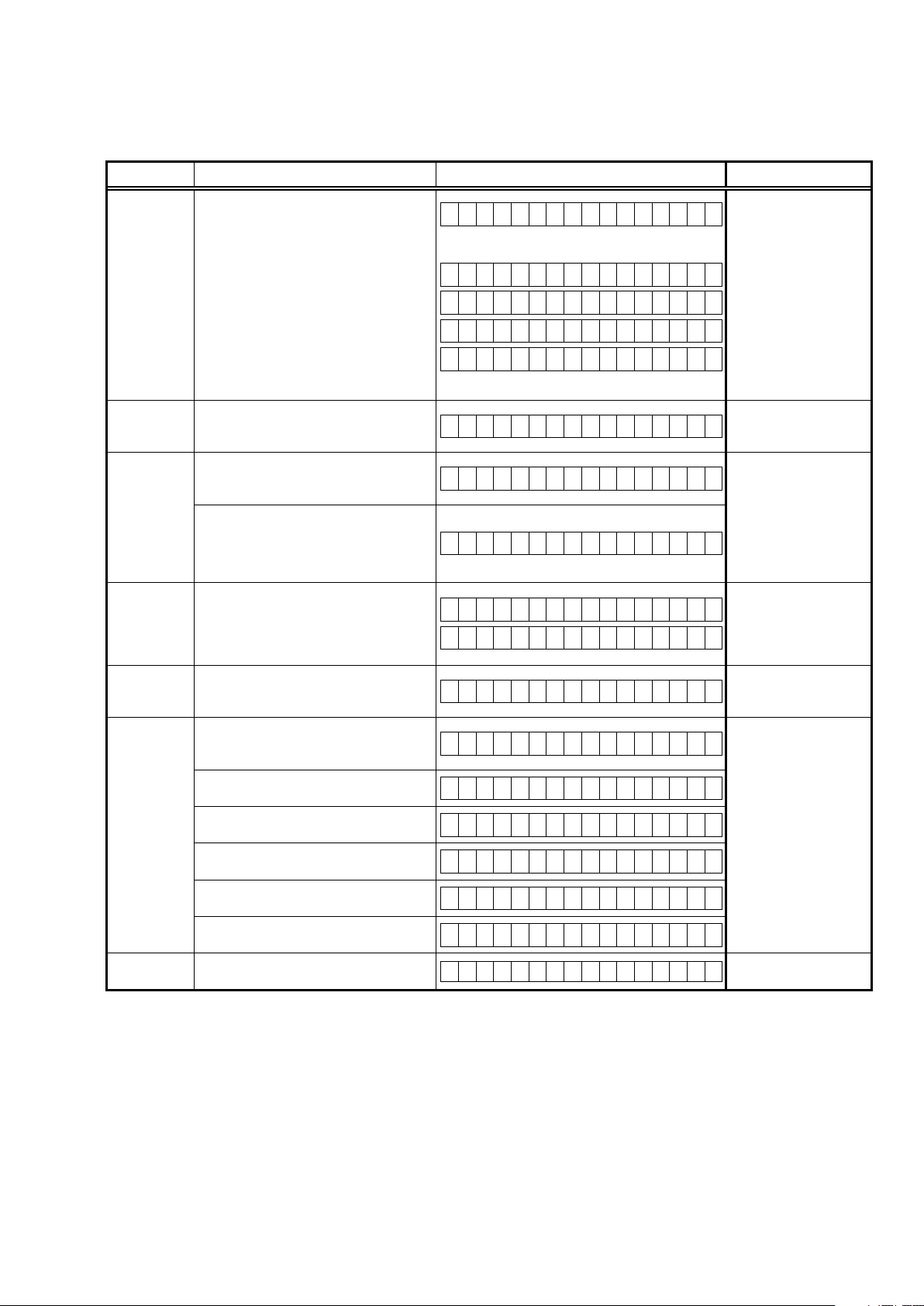
Special Mode Conguration Buttons .......................................18
1. Version Display Mode ........................................................19
2. PANEL / REMOTE LOCK Selection Mode .........................23
3. Selection Modes for Service-related Operations ................24
DIAGNOSTIC PATH DIAGRAM .........................................31
4. Remote ID Setup Mode ......................................................74
5. Protection Pass Mode ........................................................75
6. CX870 / CY920 Reboot Mode ............................................75
7. CX870 / CY920 Initialization Mode ....................................76
JIG FOR SERVICING
Procedure after Replacing the Microprocessor, etc.
Firmware Update Procedure..................................................79
1. Updating by USB ................................................................79
2. Updating by DPMS .............................................................88
ADJUSTMENT
SURROUND MODES AND PARAMETERS
TROUBLE SHOOTING
1. POWER ..............................................................................99
2. Analog video ....................................................................100
3. HDMI/DVI .........................................................................102
4. AUDIO ..............................................................................104
5. Network/Bluetooth/USB ...................................................107
6. SMPS ...............................................................................112
Audio Check PASS
...............................................................................9
.........................................................................95
.............................................................3
..........................................................6
.........................................7
...........................................................7
................................................9
.................................................................10
........................................................................11
......................................................................18
..............................................................77
..........79
............................96
............................................................99
..............................................................114
CLOCK FLOW & WAVE FORM IN DIGITAL BLOCK
LEVEL DIAGRAM
GND DIAGRAM
POWER DIAGRAM
CPU DIAGRAM
PRINTED WIRING BOARDS
SCHEMATIC DIAGRAMS (1/35 )
SCH01_DIGITAL CONNECT ................................................133
SCH02_DIR ADC ZONEDAC ...............................................134
SCH03_AUDIO PLD .............................................................135
SCH04_DSP1 .......................................................................136
SCH05_DSP2 .......................................................................137
SCH06_DSP3 .......................................................................138
SCH07_DSP4 .......................................................................139
SCH08_MAIN CPU ...............................................................140
SCH09_SUB CPU .................................................................141
SCH10_DECODER ...............................................................142
SCH11_HDMI SW1 ...............................................................143
SCH12_HDMI SW2 ...............................................................144
SCH13_IP SCALER ..............................................................145
SCH14_IP SCALER DDR .....................................................146
SCH15_VIDEO PLD .............................................................147
SCH16_HDMI RX TX ............................................................148
SCH17_HDMI SUPPLY .........................................................149
SCH18_NETWORK ..............................................................150
SCH19_AUDIO VIDEO CONNECT ......................................151
SCH20_AUDIO VOLUME .....................................................152
SCH21_PREOUT ..................................................................153
SCH22_VIDEO SELECTOR .................................................154
SCH23_CONNECT ...............................................................155
SCH24_ZONEDAC ADC .......................................................156
SCH25_MAIN DAC ...............................................................157
SCH26_FRONT HDMI USB ..................................................158
SCH27_SPEAKER ................................................................159
SCH28_REG .........................................................................160
SCH29_FRONT ....................................................................161
SCH30_SMPS ......................................................................162
SCH31_AMP CONNECT ......................................................163
SCH32_232C PHONO ..........................................................164
SCH33_POWER AMP...........................................................165
SCH34_CX870 CONNECT (CX870 Only) ............................166
SCH35_BT MODULE (CX870 Only) .....................................167
EXPLODED VIEW
PACKING VIEW
SEMICONDUCTORS
1. IC's ...................................................................................170
2. FL DISPLAY .....................................................................192
..................................................................116
.....................................................................124
................................................................125
......................................................................126
.................................................127
..........................................133
.................................................................168
.....................................................................169
.............................................................170
...........115
2
Page 3
ABOUT THIS MANUAL
Read the following information before using the service manual.
What you can do with this manual
Search for a Ref. No. (phrase)
(Ctrl+Shift+F)
You can use the search function in Acrobat Reader to
search for a Ref. No. in schematic diagrams, printed
wiring circuit diagrams, block diagrams, and parts
lists.
1.Press Ctrl+Shift+F
• The Search window appears.
2.EntertheRef.No.youwanttosearchforinthe
Search window, and then click the Search button.
•A list of search results appears.
onthekeyboard.
F
Shift
Ctrl
Jump to the target of a schematic
diagram connector
Click the Ref. No. of the target connector in the red
box around a schematic diagram connector.
•The screen jumps to the target connector.
CP401
v
CP106
3.Click an item on the list.
• The screen jumps to the page for that item, and the
searchphraseisdisplayed.
•Pagemagnicationstaysthesameasbeforethe
jump.
3
Page 4
Using Adobe Reader (Windows version)
Add notes to this data (Sign)
TheSignfunctionletsyouaddnotestothedatain
this manual.
Savetheleonceyouhavenishedaddingnotes.
[Example using Adobe Reader X]
On the "View" menu, click "Sign".
• The Sign pane appears.
[Example using Adobe Reader 9]
On the "Document" menu, click "Sign".
Magnify schematic / printed circuit
board diagrams - 1
(Ctrl+Space, mouse operation)
Press Ctrl+Spaceonthekeyboardanddragthe
mousetoselecttheareayouwanttoview.
• Theselectedareaismagnied.
0
Ctrl Space
• Whenyouwanttomovetheareashown,hold
down Space and drag the mouse.
• Whenyouwanttoshowafullpageview,press
Ctrl+0
onthekeyboard.
Print a magnied part of the manual
ThePropertiesdialogboxandfunctionswillvarydependingonyourprinter.
1. Dragthemousetomagnifythepartyouwanttoprint.
2. On the
3. CongurethefollowingsettingsinthePrintdialogbox.
"File" menu, click "Print".
• Properties
Click this button and check that the printer is set to a
suitable paper size.
• Page to print
Select the following checkbox.
"More Options" : "Current View"
• Page Sizing & Handling
Select the following checkbox.
"Size" / "Size Options" : "Fit"
4. Click the
Print button to start printing.
4
Page 5

Magnify schematic / printed circuit
board diagrams - 2
(Pan & Zoom function)
ThePan&Zoomfunctionletsyouseewhichpartof
amagnieddiagramisbeingshowninaseparate
window.
[Example using Adobe Reader X]
On the "View" menu, point to "Zoom", and then click
"Pan & Zoom".
Magnify schematic / printed circuit
board diagrams - 3
(Loupe Tool function)
TheLoupeToolfunctionletsyoumagnifyaspecic
part of a diagram in a separate window.
[Example using Adobe Reader X]
On the "View" menu, point to "Zoom", and then click
"Loupe Tool".
• The Pan & Zoom window appears on the screen.
[Example using Adobe Reader 9]
On the "Tools" menu, point to "Select & Zoom", and
then click "Pan & Zoom Window".
• The Loupe Tool window appears on the screen.
[Example using Adobe Reader 9]
On the "Tools" menu, point to "Select & Zoom", and
then click "Loupe Tool Window".
5
Page 6

SAFETY PRECAUTIONS
The following items should be checked for continued protection of the customer and the service technician.
leakage current check
Beforereturningthesettothecustomer,besuretocarryouteither(1)aleakagecurrentcheckor(2)alinetochassis
resistance check. If the leakage current exceeds 0.5 milliamps, or if the resistance from chassis to either side of the
power cord is less than 460 kohms, the set is defective.
Be sure to test for leakage current with the AC plug in both polarities, in addition, when the set's power is in each state
(on,offandstandbymode),ifapplicable.
CAUTION
Please heed the following cautions and instructions during servicing and
inspection.
Heed the cautions!
◎
Cautions which are delicate in particular for servicing
are labeled on the cabinets, the parts and the chassis,
etc. Be sure to heed these cautions and the cautions
described in the handling instructions.
Cautions concerning electric shock!
◎
(1) AnACvoltageisimpressedonthisset,soifyou
touch internal metal parts when the set is energized,
youmaygetanelectricshock.Avoidgettingan
electricshock,byusinganisolatingtransformer
and wearing gloves when servicing while the set is
energized,orbyunpluggingthepowercordwhen
replacing parts, for example.
(2) Therearehighvoltagepartsinside.Handlewith
extra care when the set is energized.
◎ Caution concerning disassembly and
assembly!
Through great care is taken when parts were
manufacturedfromsheetmetal,theremaybeburrson
theedgesofparts.Theburrscouldcauseinjuryifngers
are moved across them in some rare cases. Wear gloves
toprotectyourhands.
Use only designated parts!
◎
Theset'spartshavespecicsafetyproperties(re
resistance,voltageresistance,etc.).Besuretouseparts
which have the same properties for replacement. The
burrs have the same properties. In particular, for the
importantsafetypartsthatareindicatedbythe
on schematic diagrams and parts lists, be sure to use
the designated parts.
◎ Be sure to mount parts and arrange the wires
as they were originally placed!
Forsafetyseasons,somepartsusetapes,tubesorother
insulatingmaterials,andsomepartsaremountedaway
from the surface of printed circuit boards. Care is also
takenwiththepositionsofthewiresbyarrangingthem
andusingclampstokeepthemawayfromheatingand
highvoltageparts,sobesuretoseteverythingbackas
itwasoriginallyplaced.
z
mark
Make a safety check after servicing!
◎
Check that all screws, parts and wires removed or
disconnected when servicing have been put back in their
original positions, check that no serviced parts have
deteriorate the area around. Then make an insulation
check on the external metal connectors and between
the blades of the power plug, and otherwise check that
safetyisensured.
(Insulationcheckprocedure)
Unplug the power cord from the power outlet, disconnect
the antenna, plugs, etc., and on the power. Using a 500V
insulation resistance tester, check that the insulation
resistancevaluebetweentheinplugandtheexternally
exposedmetalparts(antennaterminal,headphones
terminal,inputterminal,etc.)is1MΩorgreater.Ifitis
less, the set must be inspected and repaired.
CAUTION
Concerning important
safety parts
Manyoftheelectricandthestructuralpartsusedinthe
sethavespecialsafetyproperties.Inmostcasesthese
propertiesaredifculttodistinguishbysight,andtheuse
ofreplacementpartswithhigherratings(ratedpower
andwithstandvoltage)doesnotnecessarilyguarantee
thatsafetyperformancewillbepreserved.Partswith
safetypropertiesareindicatedasshownbelowonthe
wiring diagrams and the parts list in this service manual.
Be sure to replace them with the parts which have the
designated part number.
(1) Schematicdiagrams .......Indicatedbythe
(2) Partslists .......Indicatedbythe
The use of parts other than the
designated parts could cause electric
shocks,resorotherdangerous
situations.
z
mark.
z
mark.
6
Page 7
NOTE FOR SCHEMATIC DIAGRAM
WARNING:
Partsindicatedbythezmarkhavecriticalcharacteristics.UseONLYreplacementpartsrecommendedbythemanufacturer.
CAUTION:
Beforereturningthesettothecustomer,besuretocarryouteither(1)aleakagecurrentcheckor(2)alinetochassisresistancecheck.
If the leakage current exceeds 0.5 milliamps, or if the resistance from chassis to either side of the power cord is less than 460 kohms, the
set is defective.
WARNING:
DONOTreturnthesettothecustomerunlesstheproblemisidentiedandremedied.
NOTICE:
ALLRESISTANCEVALUESINOHM.k=1,000OHM/M=1,000,000OHM
ALLCAPACITANCEVALUESAREEXPRESSEDINMICROFARAD,UNLESSOTHERWISEINDICATED.PINDICATESMICRO-MICRO
FARAD.EACHVOLTAGEANDCURRENTAREMEASUREDATNOSIGNALINPUTCONDITION.CIRCUITANDPARTSARESUBJECT
TOCHANGEWITHOUTPRIORNOTICE.
NOTE FOR PARTS LIST
1.Partsindicatedby
2.Whenorderingapart,makeacleardistinctionbetween"1"and"I"(i)toavoidmis-supplying.
3.Apartorderedwithoutspecifyingitspartnumbercannotbesupplied.
4.Partindicatedby"
WARNING:
Partsindicatedbythezmarkhavecriticalcharacteristics.UseONLYreplacementpartsrecommendedbythemanufacturer.
INSTRUCTIONS FOR HANDLING SEMI-CONDUCTORS AND OPTICAL UNIT
Electrostaticbreakdownofthesemi-conductorsoropticalpickupmayoccurduetoapotentialdifferencecausedby
electrostatic charge during unpacking or repair work.
"nsp" on this table cannot be supplied.
" mark is not illustrated in the exploded view.
★
1. GroundforHumanBody
Besuretowearagroundingband(1MΩ)thatisproperlygroundedtoremoveanystaticelectricitythatmaybe
chargedonthebody.
2. GroundforWorkbench
Besuretoplaceaconductivesheetorcopperplatewithpropergrounding(1MΩ)ontheworkbenchorothersurface,
wherethesemi-conductorsaretobeplaced.Becausethestaticelectricitychargeonclothingwillnotescapethrough
thebodygroundingband,becarefultoavoidcontactingsemi-conductorswithyourclothing
<Incorrect>
<Correct>
CBA
CBA
1MΩ
Grounding Band
1MΩ
Conductive Sheet or
Copper Plate
7
Page 8

Personal notes:
8
Page 9
TECHNICAL SPECIFICATIONS
Audio section
n
• Power amplifier
Rated output
Front:
140W+140W (8Ω, 20Hz - 20kHz with 0.05% T.H.D.)
175W+175W (6Ω, 1kHz with 0.7% T.H.D)
Center :
140W (8Ω, 20Hz - 20kHz with 0.05% T.H.D.)
175W (6Ω, 1 kHz with 0.7 % T.H.D.)
Surround :
140W+140W (8Ω, 20 Hz - 20 kHz with 0.05% T.H.D.)
175W+175W (6Ω, 1 kHz with 0.7 % T.H.D.)
Surround back / Height1 / Front wide / Height2:
140W+140W (8Ω, 20 Hz - 20 kHz with 0.05% T.H.D.)
175W+175W (6Ω, 1 kHz with 0.7 % T.H.D.)
Rated output :
160 W x 2-channel (8 Ω)
250 W x 2-channel (4 Ω)
Output connectors:4 - 16Ω
Analog section
n
Input sensitivity/Input impedance:200 mV/47 kΩ
Frequency response: 10 Hz - 100 kHz — +1, -3 dB(Direct mode)
S/N:102 dB(IHF-A weighted, Direct mode)
Distortion:0.005 % (20 Hz – 20 kHz) (Direct mode)
Rated output:1.2 V
Digital section
n
D/A output: Rated output — 2 V (at 0 dB playback)
Digital input:Format — Digital audio interface
Phono equalizer section
n
Input sensitivity: 2.5 mV
RIAA deviation:
S/N: 74 dB (IHF-A)
Distortion factor: 0.03 % (1 kHz, 3 V)
Video section
n
• Standard video connectors
Input/output level and impedance:
Frequency response:5 Hz – 10 MHz — 0, –3 dB
• Color component video connector
Input/output level and impedance:
Frequency response:5 Hz - 60 MHz — 0, -3 dB
:
Total harmonic distortion — 0.008 % (1 kHz, at 0 dB)
S/N ratio — 102 dB
Dynamic range — 100 dB
±1 dB (20 Hz to 20 kHz)
1 Vp-p, 75 Ω
Y signal — 1 Vp-p, 75 Ω
PB / CB signal — 0.7 Vp-p, 75 Ω
PR / CR signal — 0.7 Vp-p, 75 Ω
Tuner section
n
Reception frequency range: F M 87.5 MHz - 107.9 MHz(for E3)
Effective sensitivity:
50 dB sensitivity:
S/N ratio (IHF-A): MONO ― 78 dB
Distortion (1 kHz):
Wireless LAN section
n
Network type
(wireless LAN standard): Conforming to Wi-Fi®z1
Security:
Radio frequency:
No. of channels: 1 - 11 ch (for E3)
The Wi-Fi® CERTIFIED Logo and the Wi-Fi CERTIFIED On-Product
z1
Logo are registered trademarks of the Wi-Fi Alliance.
Bluetooth section
n
Communications system: Bluetooth Version 2.1 + EDR
Transmission power:Maximum 2.5 mW (Class 2)
Maximum communication range:Approx. 32.8 ft/10 m in line of sight
Frequency band:2.4 GHz band
Modulation scheme:FHSS (Frequency-Hopping Spread Spectrum)
Supported proles:
Corresponding codec:SBC, AAC
Transmission range (A2DP):20 Hz - 20,000 Hz
General
n
Power supply: (for E3) : AC 120 V, 60 Hz
Power consumption:730W
Power consumption in standby mode:0.1W
Power consumption in CEC standby mode:0.5W
Power consumption in network standby mode:4.5W
For purposes of improvement, specications and design are subject to
change without notice.
MONO ― 2.8 μV (20.2 dBf)
MONO ― 0.1 %
WEP 64 bit, WEP 128 bit
2.4 GHz
(for E2) : AC 230 V, 50 Hz / 60Hz
(for E1C) : AC 220 V, 50 Hz
FM 87.5 MHz - 108.0 MHz(for E2, E1C)
AM 530 kHz - 1710 kHz(for E3)
AM 522 kHz - 1611 kHz(for E2, E1C)
FM 1.5μV(14.8dBf)
AM 20 μV
STEREO ― 68 dB
HD ― FM 85dB AM 85dB
SRETEO ― 0.2 %
HD ― FM 0.02% AM 0.02%
WPA/WPA2-PSK (AES)
WPA/WPA2-PSK (TKIP)
1 - 13 ch (for E2, E1C)
(Enhanced Data Rate)
A2DP 1.2 (Advanced Audio Distribution Prole)
AVRCP 1.4 (Audio Video Remote Control Prole)
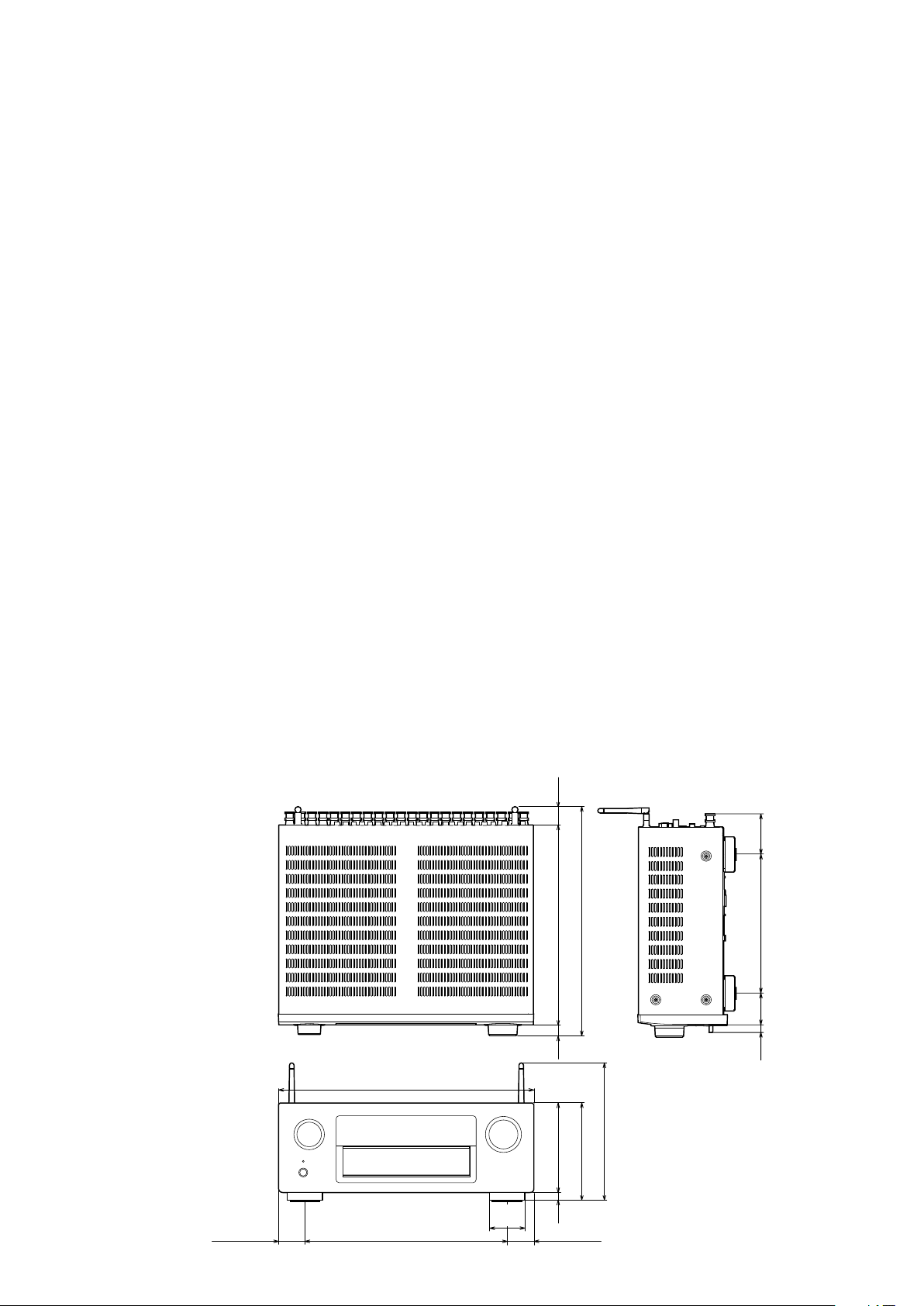
DIMENSION
Unit: in. (mm) Weight: 31 lb 1 oz (14.1 kg)
1 51/64 (45.5) 1 51/64 (45.5)
17 1/8 (435)
13 35/64 (344)
2 23/64
9
(60)
(32)
1 17/64
13 11/32 (339)
15 15/32 (393)
(22)
55/64
5 63/64 (152)
6 37/64 (167)
(15)
19/32
9 1/4 (235)
(70)
2 3/4
9 21/64 (237)
(55)
2 11/64
(12)
15/32
Page 10
PRECAUTIONS DURING SERVICE
Initializing This Unit
Initialize this unit if you have replaced the microcomputer, one of the parts around the microcomputer, or the digital PCB.
1. Press the power button to turn off the power.
2. Hold down buttons "
3. Release the buttons after conrming that the display ashes in intervals of approximately 1 second.
The unit is initialized.
*
CURSOR
" and "CURSOR
d
" at the same time and press the power button to turn on the power.
f
NOTE:
• If the status in step 3 does not occur, start again from step 1.
• Initializing the device restores settings congured by the user to the factory settings. Take note of your settings beforehand
and recongure them after initialization.
X
CURSOR
d
CURSOR
f
Service Jigs
The following jigs (extension cable kit) are used when repairing the PCBs.
Order the jigs from your dealer if necessary.
8U- 110084S : EXTENSION UNIT KIT : 2 Set
(See 77 page)
10
Page 11
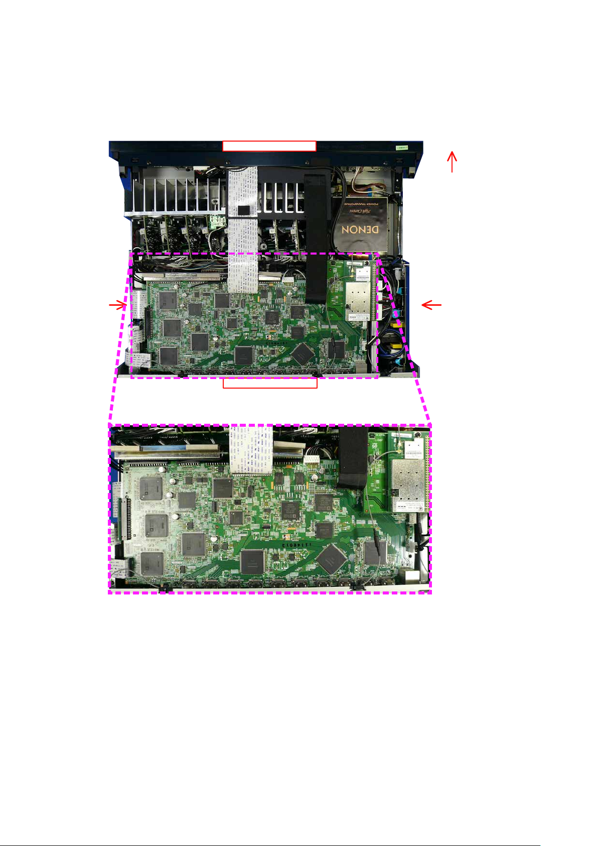
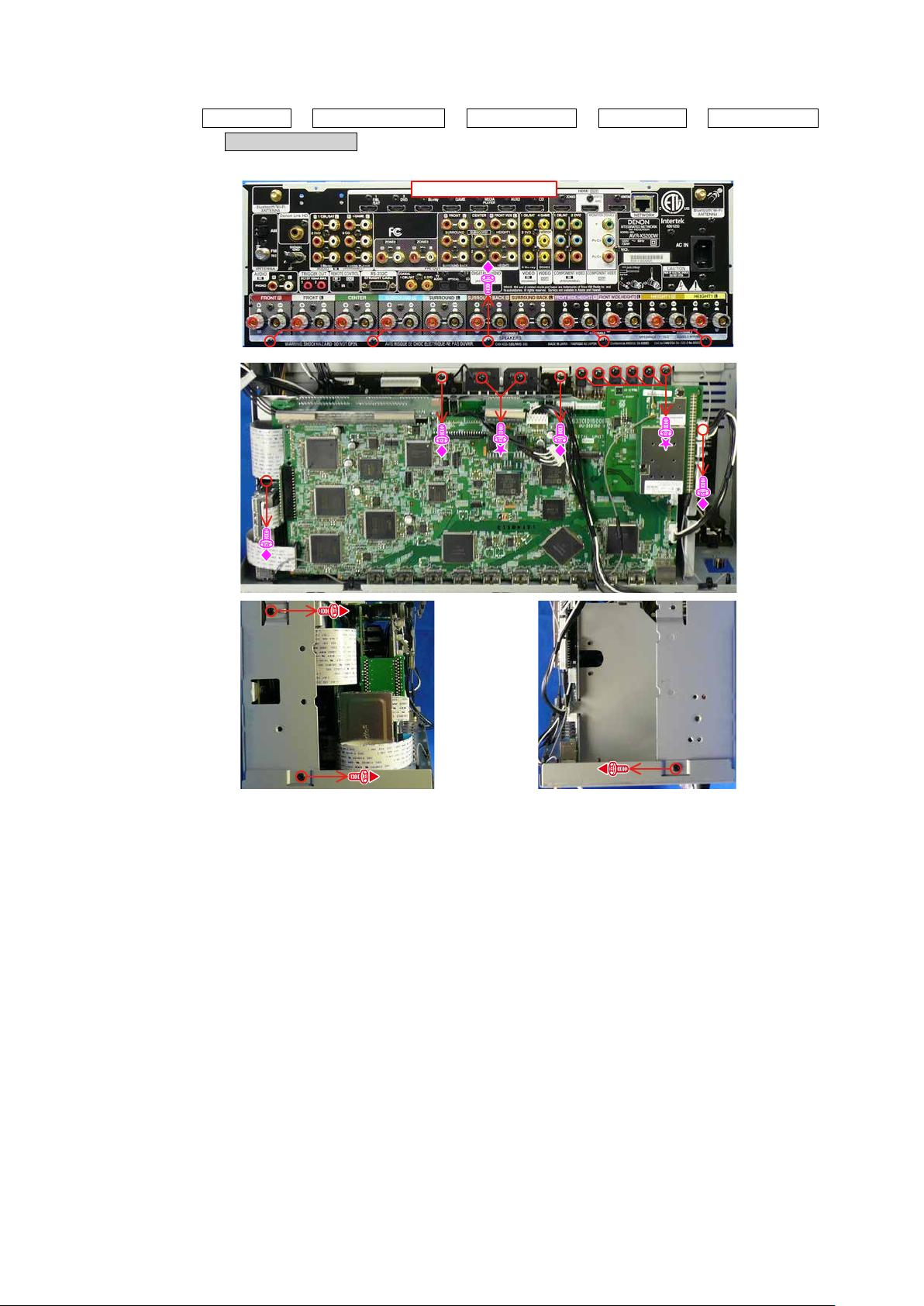
DISASSEMBLY
• Remove each part in the order of the arrows below.
• Reassemble removed parts in the reverse order.
• Read
"Precautions During Work"
• If wire bundles are removed or moved during adjustment or part replacement, reshape the wires after completing the
work. Failure to shape the wires correctly may cause problems such as noise.
before reassembling removed parts.
FRONT PANEL ASSY
See "DISASSEMBLY"
1. FRONT PANEL ASSY
and "EXPLODED VIEW"
FLD PCB
(Ref. No. of EXPLODED VIEW : C1)
HP PCB
(Ref. No. of EXPLODED VIEW : C2)
HDMI USB FRONT PCB
(Ref. No. of EXPLODED VIEW : B2)
Bluetooth PCB
(Ref. No. of EXPLODED VIEW : E1)
TOP COVER
RADIATOR ASSY
See "DISASSEMBLY"
2. RADIATOR ASSY
and "EXPLODED VIEW"
AMP PCB
(Ref. No. of EXPLODED VIEW : D)
R-AMP CONNECT PCB
(Ref. No. of EXPLODED VIEW : D1)
L-AMP CONNECT PCB
(Ref. No. of EXPLODED VIEW : D2)
RADI_PROTDET2 PCB
(Ref. No. of EXPLODED VIEW : D5)
SMPS PCB
See "DISASSEMBLY"
3. SMPS PCB
and "EXPLODED VIEW"
SMPS PCB
(Ref. No. of EXPLODED VIEW : D3)
MAIN TRANS
See "DISASSEMBLY"
4. MAIN TRANS
and "EXPLODED VIEW"
POWER TRANS
(Ref. No. of EXPLODED VIEW : 8)
BACK PANEL ASSY
See "DISASSEMBLY"
5. BACK PANEL ASSY
and "EXPLODED VIEW"
DIGITAL PCB
(Ref. No. of EXPLODED VIEW : A)
AUDIO/VIDEO PCB
(Ref. No. of EXPLODED VIEW : B)
DAC PCB
(Ref. No. of EXPLODED VIEW : B1)
CONNECTOR-1 PCB
(Ref. No. of EXPLODED VIEW : B4)
CONNECTOR-2 PCB
(Ref. No. of EXPLODED VIEW : B5)
CONNECTOR-3 PCB
(Ref. No. of EXPLODED VIEW : B6)
CONNECTOR-5 PCB
(Ref. No. of EXPLODED VIEW : B8)
SPEAKER PCB
(Ref. No. of EXPLODED VIEW : C)
HL SPEAKER PCB
(Ref. No. of EXPLODED VIEW : C3)
232C POHNO PCB
(Ref. No. of EXPLODED VIEW : D4)
CX870 CONNECT PCB
(Ref. No. of EXPLODED VIEW : E)
CX870 MODULE
(Ref. No. of EXPLODED VIEW : 59)
11
Page 12
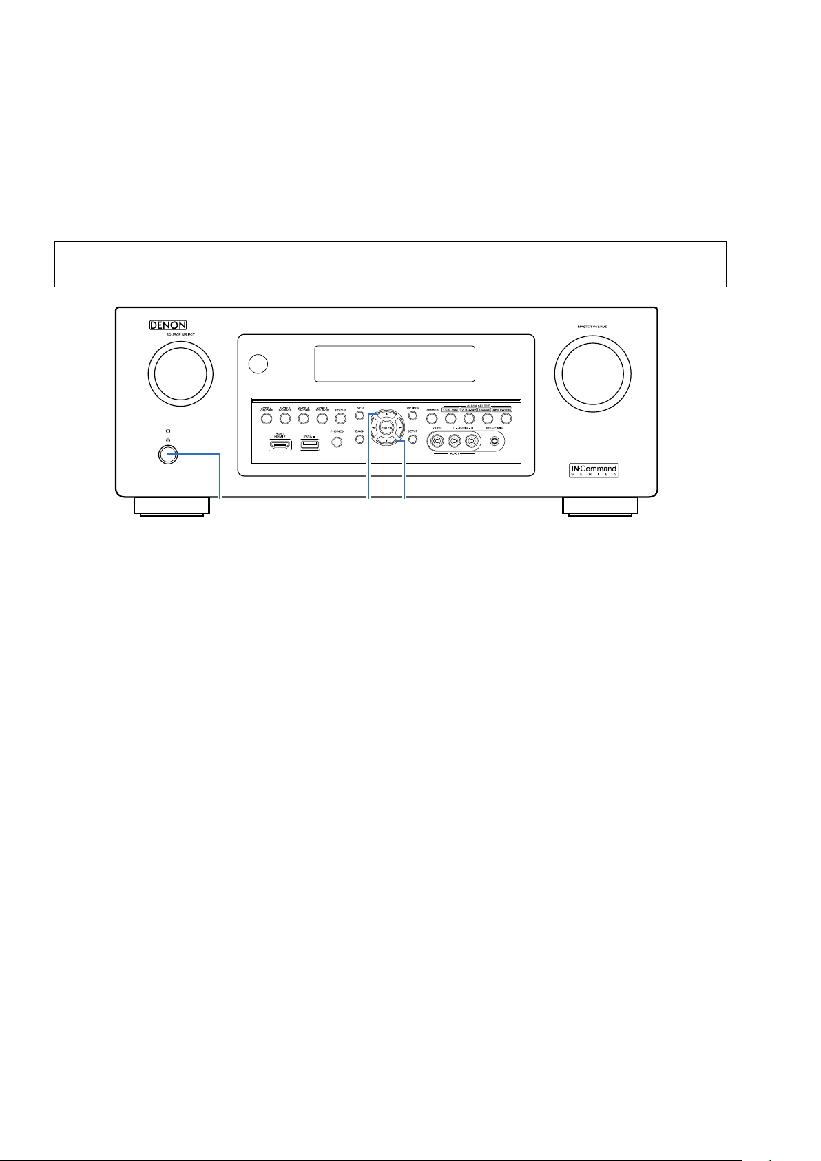
Explanatory Photos for DISASSEMBLY
• The angles from which the photos are taken are shown by "
• See the diagram below about the shooting direction of each photograph.
• Photographs with no shooting direction indicated were taken from the top of the unit.
• The photograph is AVR-X5200WE3 model.
Photo angle: A, B, C, D
The viewpoint of each photograph
(Shooting direction:X)[View from the top]
↓Shooting direction: B↓
".
Front side
Shooting
direction: D
Shooting
direction: C
↑Shooting direction: A↑
12
Page 13
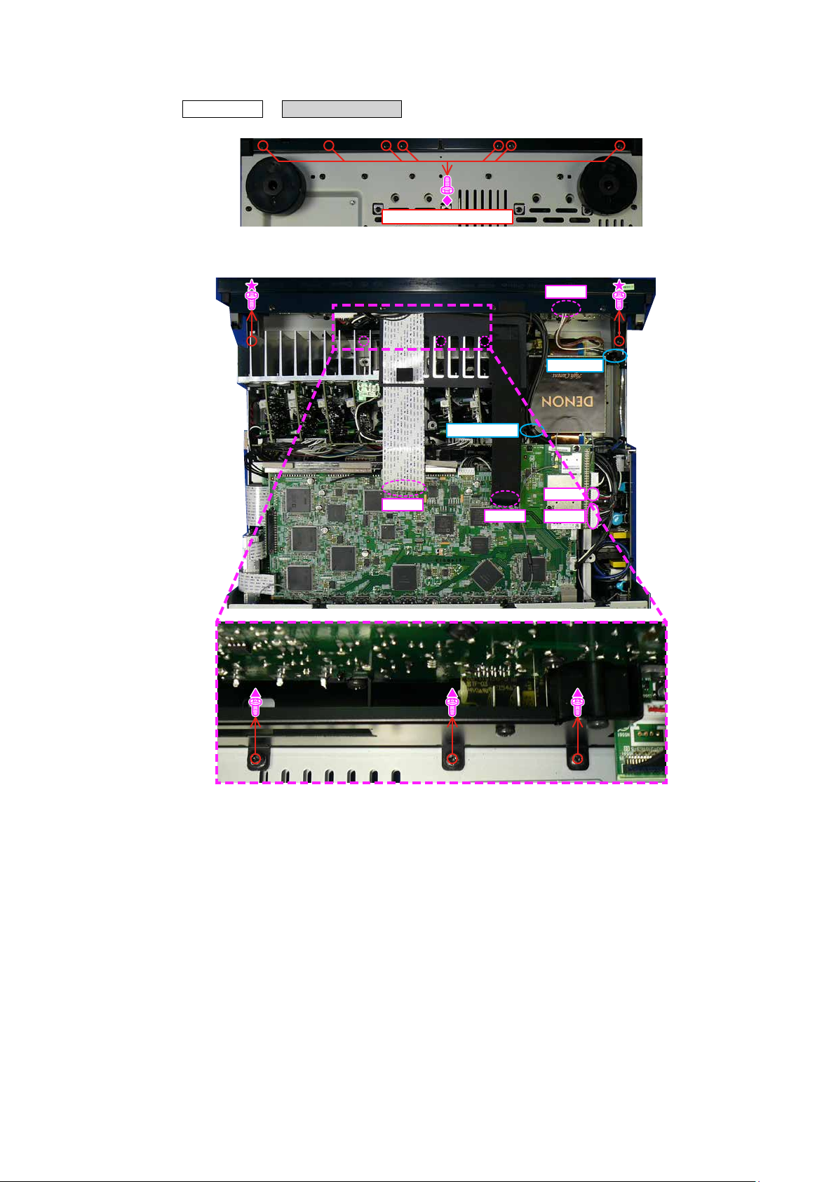
1. FRONT PANEL ASSY
Proceeding : TOP COVER → FRONT PANEL ASSY
(1) Remove the screws.
View from the bottom
(2) Remove the screws. Remove the STYLE PIN, HOLDER, FFC and connector wire.
N6401
HOLDER
STYLE PIN
FFC
FFC
N904
N901
13
Page 14
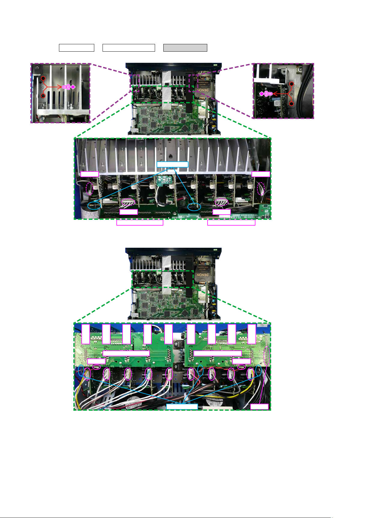
2. RADIA T OR ASSY
Proceeding : TOP COVER → FRONT PANEL ASSY → RADIATOR ASSY
(1) Remove the STYLE PIN and connector wire. Remove the screws.
STYLE PIN
N5812 N5842
N5832 N5831
(2) Remove the connector wire.
FHL
SBL
YELLOW
L-AMP CONNECT R-AMP CONNECT
L-AMP CONNECT R-AMP CONNECT
SL
GRAY
C
BROWN
BLUE
FL
RED
FR
RED
SR
BROWN
SBR
N5824N5814
FHR
GRAY
YELLOW
STYLE PIN
14
N5842
Page 15
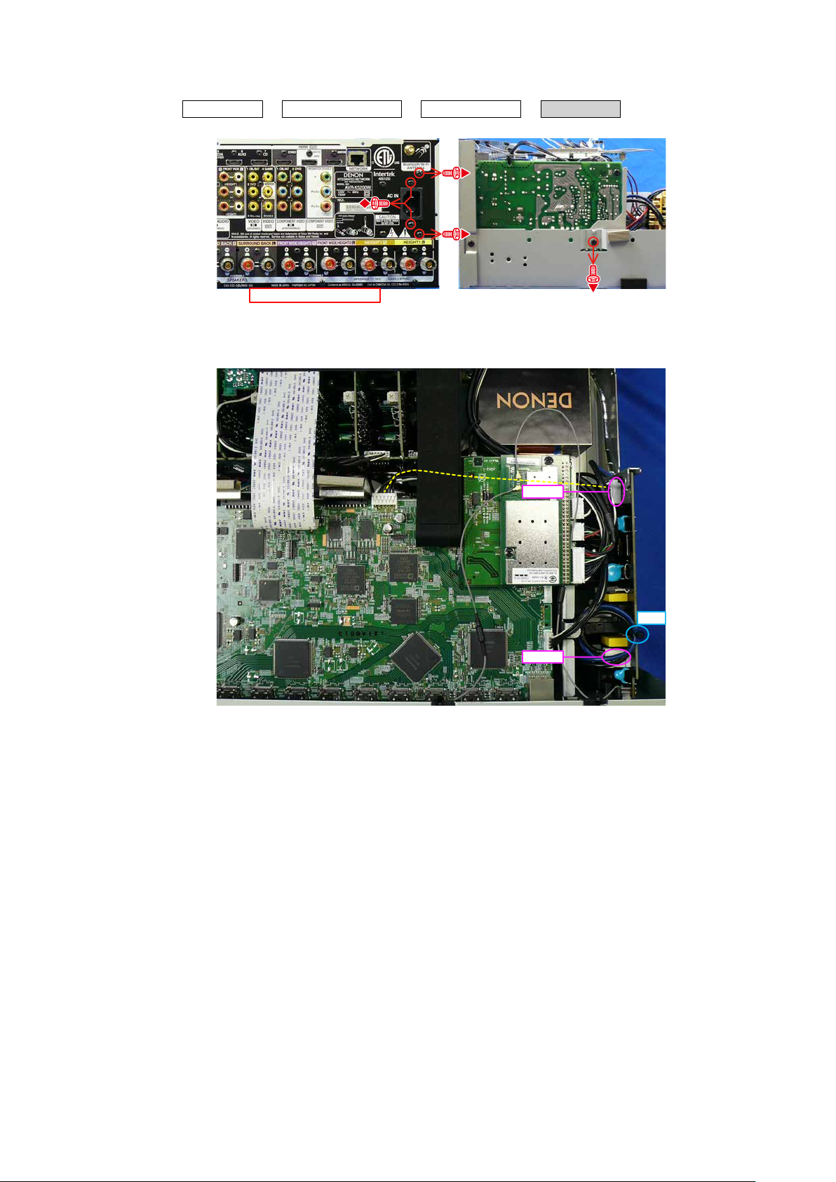
3. SMPS ASSY
Proceeding : TOP COVER → FRONT PANEL ASSY → RADIATOR ASSY → SMPS ASSY
(1) Remove the screws.
↑Shooting direction: A↑
(2) Cut the wire clamp, then remove the connector wires.
Shooting
direction: C
N6502
CUT
N6501
15
Page 16
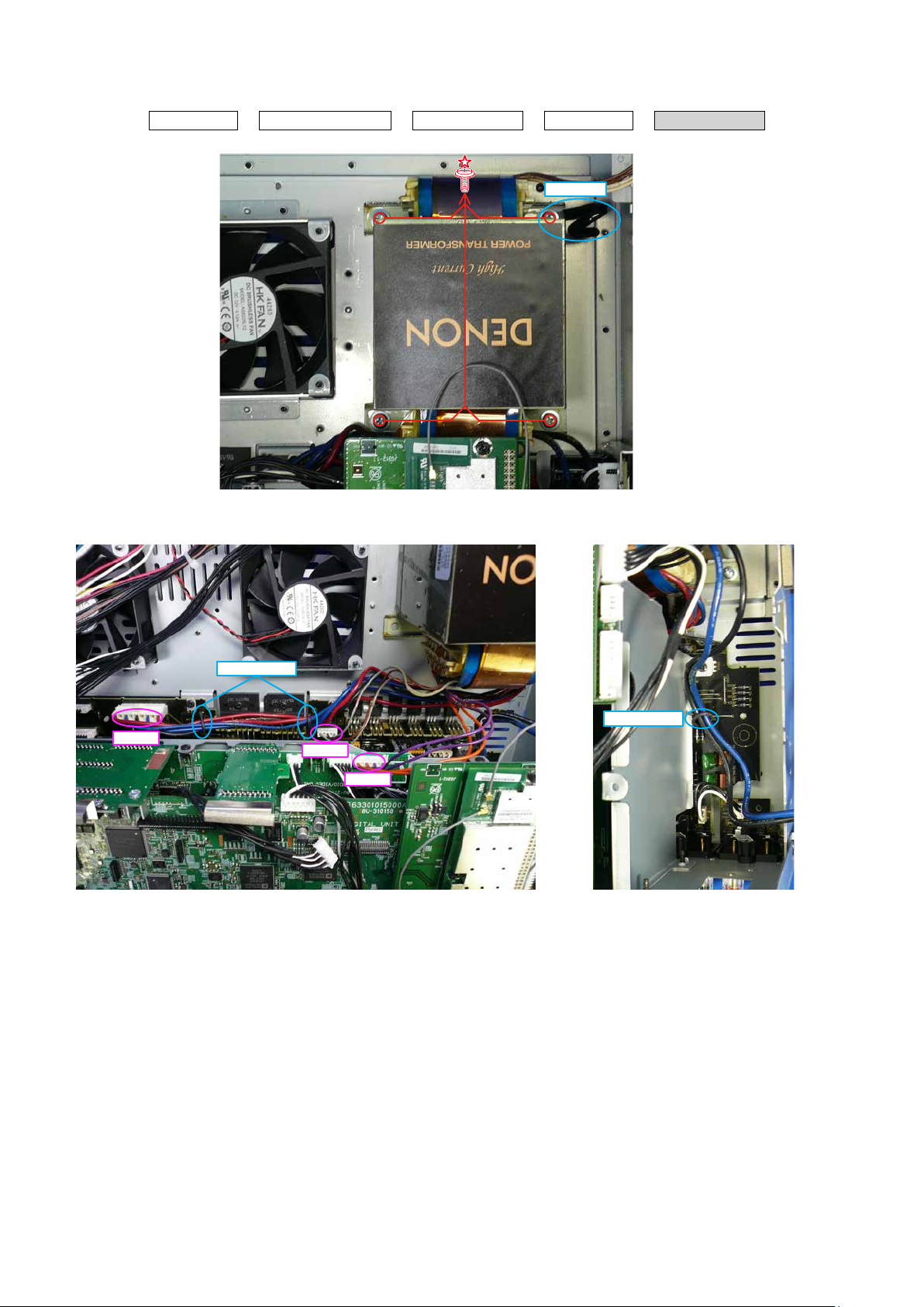
4. POWER TRANS
Proceeding : TOP COVER → FRONT PANEL ASSY → RADIATOR ASSY → SMPS ASSY → POWER TRANS
(1) Remove the screws. Remove the HOLDER.
HOLDER
(2) Remove the STYLE PIN and connector wire.
N6012
STYLE PIN
STYLE PIN
N6201
N9022
16
Page 17
5. BACK PANEL ASSY
Proceeding : TOP COVER → FRONT PANEL ASSY → RADIATOR ASSY → SMPS ASSY → POWER TRANS
→ BACK PANEL ASSY
(1) Remove the screws.
↑Shooting direction: A↑
Shooting
direction: D
Shooting
direction: C
17
Page 18
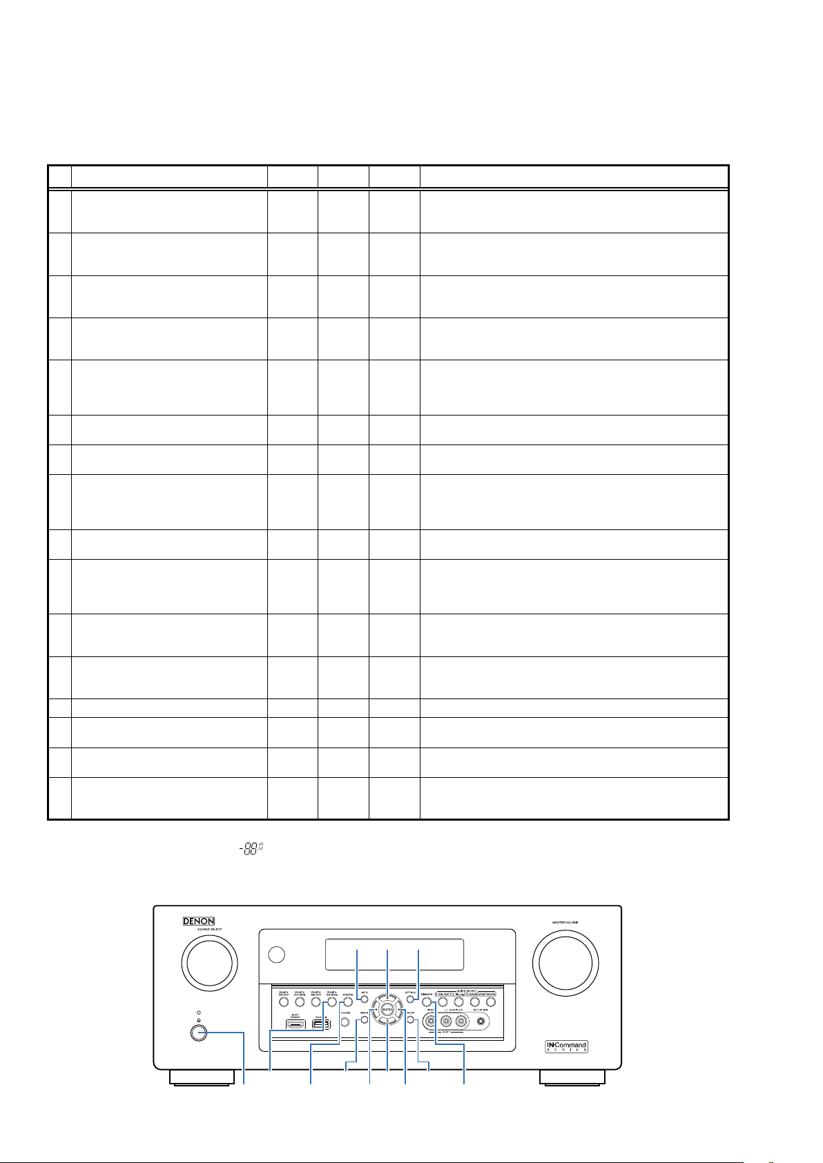
SPECIAL MODE
Special Mode Conguration Buttons
A
No. 1 - 12, 15 : Hold down buttons "
b
No. 13, 14: Hold down buttons "
b
No. 16 : Press the "
b
No. Mode Button A Button B Button C Contents
Version Display Mode
1
(u-COM / DSP Error Display)
User Initialization Mode
(Settings for the Installer Setup are not
2
initialized.)
Factory Initialization Mode
(Initialization includes settings for the
3
Installer Setup.)
PANEL / REMOTE LOCK Selection Mode
4
Check the Video/Audio pass
5
Mode
Protection History Display Mode
6
232C Standby Clear Mode
7
Operation Info Mode
8
TUNER STEP Mode
9
(E3 and E2 model only)
Remote ID Setup Mode
10
Installer Setup Mode
11
Protection Pass Mode
12
CX870 / CY920 Reboot Mode
13
CX870 / CY920 Initialization Mode
14
USB Update Mode
15
Forced USB All Device Write Mode
16
A
" and "B" buttons simultaneously while inserting the AC plug to turn the power on.
", "B" and "C" at the same time and press the power button to turn on the power.
A
" and "B" for at least 3 seconds while the power is on.
SETUP OPTION -
BACK INFO -
CURSOR dCURSOR
STATUS INFO -
STATUS
↑ ↑ -
↑ ↑ -
↑ ↑ -
↑ ↑ -
↑ ↑ -
CURSOR
0
CURSOR
0
DIMMER
DIMMER
STATUS OPTION -
STATUS OPTION -
f
ZONE3
SOURCE
BACK -
STATUS
SETUP
CURSOR
1
ZONE3
SOURCE
Displays the version of rmware such as the main rmware or DSP,
etc. Errors that have occurred are displayed.
(See 19 page)
Initializes backup data.
(Settings for the Installer Setup are not initialized.)
Initializes backup data.
-
(Initialization includes settings for the Installer Setup.)
Start this unit in the PANEL/REMOTE LOCK selection mode so that
PANEL LOCK and Remote Lock can be selected as ON or OFF.
(See 23 page)
This is a special mode for service conrmation used during repair
work to simplify the conrmation work for the Audio channel/video
-
channel.
(See 27 page)
Displays the protection occurrence history.
(See 70 page)
Switches from 232C standby mode to normal standby mode.
(See 71 page)
Displays the total operating time of the set, number of times
the power was switched on, and number of occurrences of each
protection.
(See 72 page)
Enables reception STEP of the ANALOG TUNER to be changed.
(See 73 page)
If there are multiple DENON AV receivers in the same area, this mode
stops the other AV receivers from being operated concurrently with
this device.
(See 74 page)
Access the Remote Maintenance mode via the internet.Installer Setup
is displayed on Setup menu / Network.
Refer to AVR_RemoteMaintenance_.pdf of SDI.
b
Enables the power to be turned on when protection detection is in
the stopped state.
(See 75 page)
-
Restarts CX870 / CY920. (See 75 page)
Enter this mode only after replacing Flash for CX870 / CY920 and
-
rewriting the rmware. (See 76 page)
Switches this unit to USB Update mode.
(See 79 page)
Mode used when this unit cannot be recovered.
Forcibly switches this unit to USB update mode.
(See 81 page)
NOTE :
When the volume indicator displays " ", the set has entered a special mode for developers. In this case, RS-232C communication
cannot be used.
To cancel this special mode, press and hold the "CURSOR
tor returns to the normal display, RS-232C communication can be used.
ZONE3
SOURCE
X
STATUS DIMMER
"and "STATUS" buttons for 3 seconds and longer. When the volume indica-
f
INFO OPTION
d
SETUPBACK
f
0 1
18
Page 19
1. Version Display Mode
1.1. Actions
Version information is displayed when the device is started in this mode.
1.2. Starting up
Hold down buttons "
Press the "
A version list is also displayed on GUI while the version appears on the display.
b
OPTION
" button after this to show the information in section 1.3 on the display.
1.3. Display Order
Error information(See "
→ w Firmware Package Version →
→ r Sub µ-com, Sub 1st Boot Loader Version → t DSP1/2/3/4 ROM → y Audio, Video PLD →
→ i Ethernet 1st Boot Loader, Hardware ID → o Ethernet 2nd Boot Loader, Rhapsody Flag →
→ Q1 Ethernet MAC ADDRESS information → Q2 BT MAC ADDRESS information → Q3 HD Radio(E3 only)
→ Q4 MultEQ Pro APP (Displayed when Audyssey Pro is complete) → Q5 MultEQ Pro ICL (Displayed when Audyssey Pro
is complete)
Model destination information, Serial Number :
q
FLD L1
A V R - X 5 2 0 0 W E 3 *
" and "
SETUP
1.4. Error display
OPTION
" at the same time and press the power button to turn on the power.
") →
Model destination information, Serial Number
q
Main µ-com, Main 1st Boot Loader Version
e
GUI SFLASH
u
Ethernet IMAGE
Q0
Case of CX870 : Display "*" at the end
FLD L1
FLD L1
FLD L2
Firmware Package Version :
w
FLD
Main µ-com, Main 1st Boot Loader Version :
e
FLD
Sub µ-com, Sub 1st Boot Loader Version :
r
FLD
DSP1/2 ROM :
t
FLD
DSP3/4 ROM :
FLD
A V R - X 5 2 0 0 W E 2 *
A V R - X 5 2 0 0 W E 1 C *
S / N . * * * * * * * * * *
L1
L2
L1
L2
L1
L2
L1
L2
L1
L2
F i r m . P a c k a g e
M a i n : * * . * * *
M a i n F B L : * * . * *
S u b : 7 1 1 0 * * * *
S u b F B L : * * . * *
D S P 1 : * * . * *
D S P 2 : * * . * *
D S P 3 : * * . * *
D S P 4 : * * . * *
Case of CX870 : Display "*" at the end
Case of CX870 : Display "*" at the end
V e r . : * * * *
Case of CX870 : Display "*" at the end
Audio, Video PLD :
y
FLD
L1
L2
A u d i o P L D : * * . * *
V i d e o P L D : * * . * *
19
Page 20
GUI SFLASH :
u
FLD
i
FLD
o
FLD
Q0
FLD
Q1
FLD
L1
L2
Ethernet 1st Boot Loader, Hardware ID :
L1
L2
Ethernet 2nd Boot Loader, Rhapsody Flag :
L1
L2
Ethernet IMAGE :
L1
L2
Ethernet MAC ADDRESS information :
L1
L2
G U I : 7 0 1 Z * * * *
Z
Region code(E3/E2=1, E1C=5)
:
E t h e r n e t F B L
* * * * * * - A A
AA
:Hardware ID
E t h e r n e t S B L
* * * * * * * * * * * * * - B B
E t h e r n e t I M G
* * * * * * * * * * * * *
* N E T M A C A d d r e s s
* * * * * * * - * * * * *
BT MAC ADDRESS information :
Q2
L1
FLD
HD Radio :
Q3
FLD
S
:Software Congration, R:Release Type, V:Base Version No., B:Build No.
MultEQ Pro APP :
Q4
FLD
MultEQ Pro ICL :
Q5
FLD
* B T M A C A d d r e s s
L2
L1
L2
L1
L2
L1
L2
* * * * * * - * * * * * S
* H D : S S S S S S S S -
R V V V V . B B B
* M u l t E Q P r o A P P
* * . * * . * * . * * * *
* M u l t E Q P r o I C L
* * . * * . * * . * * * *
20
Page 21
1.4. Error display
See the table below for descriptions of displayed errors and countermeasures for these.
Display order is q,w,e,r,t,y,u.
Condition States Display TROUBLE SHOOTING
The model name, brand name and region
information written in the rmware are
compared to the region settings in the
PCB.This error is displayed if the informa-
q
Firm Check
NG
w
SUB μ -COM NGThere is not a reply from SUBμ-COM.
e
IP SCALER NG
r
GUI Serial
Flash NG
t
DIR NG
y
DSP* NG
*
(
1/2/3/4)
:
u
EEPROM NG
tion does not match.
" ▲ " is displayed as the rst character if
the rmware is not correct (see right section of table).
An error occurs in Loopback Test of the
DDR memory to perform at initial setting
of i/p Scaler(ADV8003).
In initial setting of i/p Scaler ( ADV8003 ) ,
there is not the reply of the Loopback Test
result of the DDR memory .
When it is different from Version of the
Main CPU which Version of GUI Serial
Flash supports . (ADV8003)
" ▼ " is displayed as the rst character of
the GUI rmware version.
This error is displayed if there is no response from the DIR.
The DSP* FLAG0 port does not enter "Hi"
status even after executing a DSP reset
during a DSP code boot.
The DSP* FLAG0 port does not enter "Hi"
status before issuing a DSP command.
ACK="Hi" does not occur during DSP*
data reading, even when WRITE="Lo".
ACK="Lo" does not occur during DSP*
data reading, even when REQ="Lo".
ACK="Hi" does not occur during DSP*
data writing, even when WRITE="Hi".
ACK="Lo" does not occur during DSP*
data writing, even when REQ="Lo".
An error occurred in a checksum of the
EEPROM(*** is a block address number).
F I R M E R R O R
–
M a i n : * * . * *
–
D S P 1 : * * . * *
–
A u d i o P L D : * * . * *
–
G U I : * * * * * * * *
S U B E R R O R 0 1
I P S C A L E R E R R 0 1
I P S C A L E R E R R 0 2
G U I V E R . E R R O R
•
G U I : * * * * * * * *
D I R E R R O R 0 1
D S P * E R R O R 0 1
D S P * E R R O R 0 2
D S P * E R R O R 0 3
D S P * E R R O R 0 4
D S P * E R R O R 0 5
D S P * E R R O R 0 6
E 2 P R O M E R R * * *
• Check the resistor for
setting region(R5003,
R5004, R5006, R5007,
R5013, R5014 DIGITAL
PCB).
• Write the rmware for
the correct region.
• Check the SUB(U2101)
and surrounding
circuits.
• Check the circuits
around the IP SCALER
(U2800, DIGITAL PCB)
and DDR2 (U3000/
U3001).
If there appear to be
no problems, U2800 or
U3000/U3001 is faulty.
• Check the rmware
version.
• Check the DIR (U1000,
DIGITAL PCB) and surrounding circuits.
• Check the DSP (U101,
U201, U301, U401, DIGITAL PCB) and surrounding circuits.
21
Page 22
1.5. Version Display in the Setup Menu
Follow the steps below to display the rmware information.
(1) Press the "
(2) Select "
SETUP" button on the remote control.
General - Information - Firmware
".
The version information is displayed as a 14-digit number as shown in the screenshot below.
General/Firmware
Version
GUI Image
XXXX - XXXX - XXXX - XX
This 14-digit number comprises part of the version number of each device and module.
These version numbers correspond to the 14-digit number as shown below.
The 2nd digit from the right for Main
The 1th digit from the right for Main
The 2nd digit from the right for Sub
The 1st digit from the right for Sub
Main
Sub
DSP1
DSP2
DSP3
DSP4
A.PLD
V.PLD
GUI
E.FBL
E.SBL
E.IMG
X
8X 3 8- 3 8 21
X X X 0 0 2 8
X X X
X X X
X X X
X X X
X X X
X X X
2
3
4
5
1
7
X X X X 0 0 1 6
The 1st digit from the right for DSP1
The 1st digit from the right for DSP2
The 1st digit from the right for DSP3
The 1st digit from the right for DSP4
The 1st digit from the right for A.PLD
The 1st digit from the right for V.PLD
The 1st digit from the right for GUI
X X X X X X
XB X X X X X X X X X X X
XI X X X X X X X 0 0 3 7
Info display 2 3 4 - 6 7 7 3 - 0 5
The 1st digit from the right for IMG
The 2nd digit from the right for IMG
The rmware version numbers and this 14-digit version information are written in the Service Information.
b
22
Page 23
2. PANEL / REMOTE LOCK Selection Mode
2.1. Actions
Turn the PANEL LOCK and REMOTE LOCK modes on and off.
2.2. Starting up
Hold down buttons "STATUS" and "INFO" at the same time and press the power button to turn on the power.
Select the mode using the button "CURSOR
2.3. Displaying and Selecting Each Mode
The information shown on the display changes each time the button "CURSOR
Press the button "ENTER" to set the currently displayed mode and restart the device.
The On/Off setting for each mode is shown by an asterisk "*".
q
L1
FLD
The buttons on the unit and the master volume knob cannot be operated.
w
FLD
The buttons on the unit cannot be operated.
e
FLD
The PANEL LOCK mode is turned off.
r
FLD
The device cannot be operated by the remote control.
t
FLD
The REMOTE LOCK mode is turned off.
– F P / V O L L O C K * O n
L2
L1
L2
L1
L2
L1
L2
L1
L2
F P L O C K O n
F P / V O L L O C K * O n
– F P L O C K O n
F P L O C K * O n
– F P L O C K O f f
F P L O C K O f f
– R C L O C K O n
R C L O C K O n
– R C L O C K O f f
", and press the button "ENTER" to commit the selection.
f
" is pressed.
f
23
Page 24
3. Selection Modes for Service-related Operations
3.1. Actions
Select diagnostic mode (service path check mode), protection history display mode, or 232C standby clear mode.
3.2. Starting up
Hold down buttons "STATUS" and "ZONE3 SOURCE" at the same time and press the power button to turn on the power.
Select the mode using the button "CURSOR
3.3. Displaying and Selecting Each Mode
The information shown on the display changes each time the button "CURSOR
Press the button "ENTER" to set the currently displayed mode and restart the device.
q
L1
FLD
Service Path Check Mode:
The Video and Audio paths can be checked.
This function is convenient for conrming problem paths in the product and executing a path
w
FLD
The protection history can be checked.
– 1 . S E R V I C E C H E C K
L2
L1
L2
2 . P R O T E C T I O N
check after repair.
1 . S E R V I C E C H E C K
– 2 . P R O T E C T I O N
", and press the button "ENTER" to commit the selection.
f
" is pressed.
f
e
FLD
Switches from 232C standby mode to normal standby mode.
r
FLD
Operation Info for the unit can be checked.
t
FLD
Enables reception STEP of the ANALOG TUNER to be changed.
y
FLD
Function to operate only the desired AV receiver.
L1
L2
L1
L2
L1
L2
L1
L2
2 . P R O T E C T I O N
– 3 . R S 2 3 2 C R E S E T
3 . R S 2 3 2 C R E S E T
– 4 . O P I N F O
4 . O P I N F O
– 5 . T U N E R F R Q S E T
5 . T U N E R F R Q S E T
– 6 . R E M O T E I D
3.3. Canceling the mode
Press the power button to turn off the power.
24
Page 25

Personal notes:
25
Page 26
3.4 PROTECTION DIAGRAM
AVR-X5200 ASO/DC/THERMAL PROTECTION DIAGRAM
8U-110157-1 P.AMP UNIT
TR Thermal
FL
TR Thermal
C
TR Thermal
SL
TR Thermal
ASO
ASO
ASO
ASO
N101
13P-SOCKET(C125Z2)
+B
TR_THERMAL_A
ASODET
+B
TR_THERMAL_A
ASODET
+B
TR_THERMAL_A
ASODET
+B
8U-110157-5 L AMP CONNECT UNIT
N5801
13P-PLUG(C125Z1)
31
13
21
12
11
11
01
10
9
9
8
8
7
7
6
6
5
5
4
4
3
3
2
2
1
1
8U-110157-1 P.AMP UNIT
TR Thermal
FR
TR Thermal
SR
TR Thermal
SBR
TR Thermal
ASO
ASO
ASO
ASO
N101
13P-SOCKET(C125Z2)
+B
TR_THERMAL_B
ASODET
+B
TR_THERMAL_B
ASODET
+B
TR_THERMAL_B
ASODET
+B
8U-110130-10 R AMP CONNECT UNIT
N5805
13P-PLUG(C125Z1)
31
13
21
12
11
11
01
10
9
9
8
8
7
7
6
6
5
5
4
4
3
3
2
2
1
1
8U-310150 DIGITAL UNIT
102
103
104
105
106
107
FANDET_HIGH
FANDET_ON
ASODET
DCDET
TRDET
AMPSIGDET
CURRENTDET
108
PE1
PE0
109
PD7
110
PD6
111
PD5
112
PD4
113
P64
114
P63
115
P62
116
P61
117
P60
118
PD3
119
PD2
120
PD1
121
PD0
122
P97
123
P96
124
P95
125
P94
126
P93
127
P92
128
P91
129
VSS
130
P90
131
VCC
132
P47
133
P46
134
P45
135
P44
136
P43
137
P42
138
P41
139
VREFL
140
P40
141
VREFH
142
AVCC
143
P05
144
P042P033P674P665AVSS6P027P018P009P6510EMLE11WDTOVF#12VSS13MDE14VCL15MD116MD017P8618P8519RES#20XTAL21VSS22EXTAL23VCC24NMI25P3426P3327P3228P3129P3030P2731P2632P2533P2434P2335P2236P21
1
PE7
PE6
PE5
PE4
PE3
PE2
NC
SWM3.3V
100
101
PA1
PA0
R5F56108VNFP
2
9
PB093VSS94PA795PA696PA597PA498PA399PA2
U5001
THERMALINF
73
PC374VCC75PC276VSS77PC178PC079PB780PB681PB582PB483PB384PB285PB186P7487P7388P7289P7190P7091VCC
72
PC4
71
PC5
70
PC6
69
PC7
68
P75
67
P76
THERMALINE
66
P77
65
P50
64
P51
63
P52
62
BCLK
61
P80
60
P81
59
VCC
58
P82
57
VSS
56
P83
55
P54
54
P55
53
P56
52
P57
51
P84
50
P35
49
P36
48
P37
47
P10
46
P11
45
P12
44
P13
43
P14
42
P15
41
PLLVSS
40
P16
39
PLLVCC
38
P17
37
P20
SBL
TR Thermal
FHWL
Z5801
C5801
Z5802
1/100
1/100
A+7V.
UDZS3.6B
D6023
C5802
Z5803
C5803
Z5804
C5804
B5801
M3-SIDE
R6081 10K
R6082
R6083 10K
R6084
D6025
KDS160
10K
10K
Radiator
Thermal
8U-110156-1 SPK UNIT
CURRENT DETECTION THRESHOLD
16.3Arms(7.3Adc) -> Shut down
5.6Arms (2.5Adc) -> Fans highly operate , Change +B voltage
3.9Arms (1.8Adc) -> Fans operate
C6023
+B
0.01
V load
R6060
C6024
Current
Detection
R6079
33K
0.1
C6021
100/16
C6022 0.1
C6025
ASO
PRF18BB471QB5RB
4.7u
PRF18BB471QB5RB
4.7u
PRF18BF471QB5RB
4.7u
PRF18BF471QB5RB
4.7u
C6026
OPEN
U6001
NJM8080G
R6087
3.3K
N5816
4P-PH-SAN
PROTECTION LOGIC
DCDET :L -> Shut down
ASODET :L -> Shut down
TRDET :L -> HiB -> LoB
ThermalDET :L -> Shut down
FANDET_ON :L -> Fans operate
FANDET_HIGH :L -> Fans
highly operate
5
7
8
U6001
6
NJM8080G
R6089
C6063
3
4
1
2
R6088
330K
C6062
OPEN
1
1
2
2
3
3
4
4
10K
OPEN
10K
R6090
CURRENTDET
TR_THERMAL_A
+B
TR_THERMAL_A
RADI_PROTDET_E
RADI_PROTDET_F
FANDET_ON
FANDET_HIGH
5185N
sHP-P4
1K
R6091
C6027
1/100
33K
R6092
ASODET
ASODET
Radiator
Thermal
R6001
82K
N6010
11P-PH
FANDET_HIGH
KTC3875S
Q6001
R6003
82K
RADI_PROTDET_F
RADI_PROTDET_E
FANDET_ON
FANDET_HIGH
FANGND
FAN+B
AMPGND
123456789
123456789
AMPGND
THERMALDET_E
FANDET_HIGH
THERMALDET_F
FANDET_ON
FAN+12V-1
FANGND
FANDET_ON
THERMALDET_F
KTC3875S
KTC3875S
Q6003
Q6006
R6005
0
R6009
R6014
0
R6012
R6007
220K
220K
RLYB+12V
FHWL
TR_THERMAL_B
ASODET
Radiator
Thermal
TEMPERATURE THRESHOLD
RADIATOR
125 degree -> Shut down
105 degree -> Fans highly operate
75 degree -> Fans operate
TR_THERMAL_A
-FILTB
ASODET
N5812
11P-PHs
10
11
10
11
-FILTB
ASODET
TR_THERMAL_A
THERMALDET_E
KTC3875S
Q6008
0
POWER TR
100 degree -> Change +B Voltage
KTC3875S
Q6010
10K
10K
10/63
10/63
C6004
R6018
C6005
R6019
DCASOTR Thermal
From Power Amp Output
FR ch
FL ch
C ch SBR ch
0.1
100K
KTC3875S
KTC3875S
KTC3875S
Q6012
Q6011
3.3K
47/25
C6006
R6020
TRDET
ASODET
KTA1504S
R6032
C6008
Q6015
Q6013
Q6014
KTC3875S
330/10
15K
C6007
R6022
PRF18BB471QB5RB
Z5805
C5805
4.7u
Z5806
PRF18BB471QB5RB
C5806
4.7u
Z5807
PRF18BF471QB5RB
C5807
4.7u
Z5808
PRF18BF471QB5RB
C5808
4.7u
RADI_PROTDET_E
B5802
M3-SIDE
SR ch
SL ch
KTC3875S
Q6016
330/10
15K
R6038
C6009
RADI_PROTDET_F
0.1
100K
KTA1504S
KTC3875S
C6010
R6040
Q6019
Q6018
Q6017
KTC3875S
330/10
C6013
4P-PH-SAN
FANDET_O
FANDET_HIGH
SBL ch
FHWR ch
FHWL ch
0.1
100K
R6055
Q6020
KTC3875S
15K
R6050
N5826
RADI_PROTDET_E
1
1
RADI_PROTDET_F
2
2
FANDET_ON
3
3
FANDET_HIGH
4
4
5285N
KTA1504S
Q6021
DCDET
sHP-P4
N5822
N6011
FANDET_ON
FANDET_HIGH
OPEN
Q6002
OPEN
R6006
OPEN
OPEN
R6004
R6002
RLYB+12V
Radiator
Thermal
12P-PHs
12P-PH
Q6004 OPEN
OPEN
OPEN
R6008
ASODET
TR_THERMAL_B
ASODET
TR_THERMAL_B
OPEN
THERMALDET_F
Q6007
R6010
OPEN
R6013
AMPGND
FANDET_ON
-FILTB
RADI_PROTDET_F
RADI_PROTDET_E
FANDET_HIGH
FAN+12V
FANGND
987654321
121110
987654321
121110
N6013
SWM3.3V
33P-FFC
CURRENTDET
-FILTB
AMPGND
FAN+12V
FANGND
FANDET_ON
FANDET_HIGH
THERMALDET_F
THERMALDET_E
OPEN
THERMALDET_E
Q6009
R6015
OPEN
OPEN
R6017
TEHRMALDET_E
THERMALDET_F
FANDET_ON
FANDET_HIGH
BRL_HIGH
FANCONT_ON2
FANCONT_L_ON2
FANCONT_ON1
FANCONT_L_ON1
SPRL_F
SPRL_C
SPRL_S
SPRL_SB
SPRL_F_SB
SPRL_F_W
SPRL_W_SB
SPRL_W
SPRL_SB_W
SPRL_W_H
AMPSIGDET
TRDET
DCDET
ASODET
A-7V
A-7V
A+7V
A+7V
DGND
DGND
PREPOWERGND
PREPOWERGND
N
C6016
8U-210163-3
CONNECT-1_UNIT
33
1
CURRENTDET
32
2
THERMALDET_E
31
3
30
4
FANDET_ON
29
5
FANDET_HIGH
28
6
27
7
26
8
25
9
24
10
23
11
22
1
2
21
13
20
14
19
15
18
16
17
17
16
18
15
19
14
20
13
21
12
22
11
10
9
8
7
6
5
4
3
2
1
TRDET
23
DCDET
24
ASODET
25
26
27
28
29
30
31
32
33
33P-FFCs
N3003
CURRENTDET
17
17
SWM3.3V
TRIG12V
CURRENTDET
17
17
SWM3.3V
TRIG12V
CURRENTDET
CURRENTDET
TRDET
DCDET
ASODET
AMPSIGDET
R5062100
R5063100
R5061100
10111213141516
10111213141516
<- Pulled down by 1Mohms
123456789
N5003
123456789
17P-PLUG(C125Z1)
N5905
FANDET_ON
THERMALINE
THERMALINF
FANDET_HIGH
R5057100
R5056100
R5060100
R5059100
17P-SOCKET(C125Z2)
FANDET_ON
AMPSIGDET
TEHRMALE
FANDET_ON
ASODET
AEXP_CLK
FANDET_HIGH
AMPSIGDET
THERMALF
DCDET
TRDET
10111213141516
10111213141516
DCDET
TRDET
TEHRMALE
THERMALF
FANDET_ON
AMPSIGDET
FANDET_HIGH
THERMALDET_E
THERMALDET_F
FANDET_ON
FANDET_HIGH
AMPSIGDET
TRDET
DCDET
AEXP__OE
DGND
DGND
AEXP_STB
AEXP_DATA
N5906
17P-PLUG(C125Z1)
123456789
123456789
N9018
17P-SOCKET(C125Z2)
DGND
ASODET
ASODET
DGND
AEXP_CLK
AEXPDATA
AEXP__OE
AEXP_STB
26
Page 27
3.5. DIAGNOSTIC MODE (Service Path Check Mode)
3.5.1. Actions
This function is convenient for conrming problem paths in the product and executing a path check after repair.
The Video and Audio paths can be checked.
The backup data is not rewritten.
3.5.2. Starting up
Hold down buttons "STATUS" and "ZONE3 SOURCE" at the same time and press the power button to turn on the power.
Select "1. SERVICE CHECK" and press the "ENTER" button to start the diagnostic mode.
The "TUNED", "STERO" and "RDS" segments are lit in this mode.
3.5.3. Canceling diagnostic mode
Press the power button to turn off the power.
3.5.4. Selecting items
Press
Press button
button to switch between video items and audio items.
q
or
w
Actions
Button DIMMER CURSOR
to select the previous or next item.
e
The unit Remote control unit
q w e q w e
Audio ⇔ Video PREVIOUS NEXT Audio ⇔ Video PREVIOUS NEXT
0
CURSOR
1
SLEEP CURSOR
0
CURSOR
3.5.5. Audio system conrmation items
g. XX: See the block diagram of the g.XXth.
1
Paths conrmation item Display Settings Contents of conrmation Remarks
Analog
(MAIN ZONE)
1
Digital
(MAIN ZONE)
2
Digital (signal) Path
(ZONE2)
3
Digital (signal) Path
(ZONE3)
4
HDMI
(MAIN ZONE)
5
g.01
g.02a
g.02b
g.03a
g.03b
g.03c
g.04a
g.04b
g.05a
g.05b
g.05c
A 0 1 : A N A L O G P A S S
A 0 2 : D I G I T A L
A 0 3 : D I G I T A L - Z 2
A 0 4 : D I G I T A L - Z 3
A 0 5 : H D M I
Input Source : CBL/SAT
Input Mode : Analog(xed)
Sound mode : Direct
Vol. : 60.0(-20.0dB)
Amp assign : 9.1ch
ZONE2 : OFF
ZONE3 : OFF
Input Source : CBL/SAT
Input Mode : Digital(xed)
Sound mode : Multi Ch Stereo
Vol. : 60.0(-20.0dB)
Amp assign : 9.1ch
Speaker Select : Floor
Speaker Cong : All Speaker=Small/Subwoofer=2spkrs
ZONE2 : OFF
ZONE3 : OFF
Input Source : Online Music
Input Mode : Auto
Sound mode : Stereo
Amp assign : 7.1ch + ZONE2
Speaker for ZONE2 : SURROUND BACK
ZONE2 : ON
ZONE2 Source : Source
Z2 Vol. : 60.0(-20.0dB)
ZONE3 : OFF
Input Source : Online Music
Input Mode : Auto
Sound mode : Stereo
Amp assign : 7.1ch + ZONE3
Speaker for ZONE3 : FRONT WIDE/HEIGHT 2
ZONE2 : OFF
ZONE3 : ON
ZONE3 Source : Source
Z3 Vol. : 60.0(-20.0dB)
Input Source : CBL/SAT
Input Mode : HDMI(xed)
Sound mode : Stereo
Vol. : 60.0(-20.0dB)
Amp assign : 9.1ch
ZONE2 : OFF
ZONE3 : OFF
・Analog input ⇒ Speaker output (Front L/R)
・Analog input ⇒ Preout output (Front L/R)
(bAs the input source, you can switch from CBL/SAT to other ones.)
・Digital input ⇒ Speaker output (Front L/R, Center, Surround L/R, Surround Back L/R)
・Digital input ⇒ Preout output (Front L/R, Center, Subwoofer1/2, Surround L/R, Surround Back L/R)
(bAs the input source, you can switch from CBL/SAT to other ones.)
・Digital(PCM) input ⇒ Speaker output (Surround Back L/R → ZONE2 L/R)
・Digital(PCM) input ⇒ Preout output (ZONE2 L/R)
(bAs the input source, you can switch from Online Music to other ones.)
・Digital(PCM) input ⇒ Speaker output (Front Wide/Height2 L/R → ZONE3 L/R)
・Digital(PCM) input ⇒ Preout output (ZONE3 L/R)
(bAs the input source, you can switch from Online Music to other ones.)
・HDMI Input ⇒ Speaker output (Front L/R)
・HDMI Input ⇒ Preout output (Front L/R)
(bAs the input source, you can switch from CBL/SAT to other ones.)
27
Page 28
Paths conrmation item Display Settings Contents of conrmation Remarks
A/D
(MAIN ZONE)
6
Amp Assign
(ZONE2)
7
Amp Assign
(ZONE3)
8
Amp Assign
(ZONE2/ZONE3-MONO)
9
Amp Assign
(7.1ch (Bi-Amp)
10
Front Height
11
Front Wide
12
g.06a
g.06b
g.07
g.08
g.09
g.10a
g.10b
g.11a
g.11b
g.12a
g.12b
A 0 6 : A D
A 0 7 : A S S I G N - Z 2
A 0 8 : A S S I G N - Z 3
A 0 9 : A S S I G N - Z 3 / 3 M
A 1 1 : A S S I G N - B i A M P
A 1 4 : F R O N T H E I G H T
A 1 5 : F R O N T W I D E
Input Source : CBL/SAT
Input Mode : Analog(xed)
Sound mode : Multi Ch Stereo
Vol. : 60.0(-20.0dB)
Amp assign : 9.1ch
Height Speakers=2 Height Speakers
Height Layout=Front Height
Speaker Select : Floor
Speaker Cong : All Speaker=Small/Subwoofer=2spkrs
ZONE2 : OFF
ZONE3 : OFF
Input Source : CBL/SAT
Input Mode : Auto
Sound mode : Stereo
Amp assign : 7.1ch + ZONE2
Speaker for ZONE2 : Surround Back
ZONE2 : ON
Z2 Source : Source
Z2 Vol : 60(-20dB)
ZONE3 : OFF
Input Source : CBL/SAT
Input Mode : Auto
Sound mode : Stereo
Amp assign : 7.1ch + ZONE3
Speaker for ZONE3 : FRONT WIDE/HEIGHT 2
ZONE2 : OFF
ZONE3 : ON
ZONE3 Source : Source
Z3 Vol. : 60.0(-20.0dB)
Input Source : CBL/SAT
Input Mode : Auto
Sound mode : STEREO
Amp assign : 7.1ch + ZONE2/3-MONO
Speaker for ZONE2/3 : HEIGHT1
ZONE2 : ON
Z2 Source : Source
Z2 Vol : 60(-20dB)
ZONE3 : ON
Z3 Source : Source
Z3 Vol : 60(-20dB)
Input Source : CBL/SAT
Input Mode : Auto
Sound mode : Multi Ch Stereo
Vol. : 60.0(-20.0dB)
Amp assign : 7.1ch (Bi-Amp)
Speaker for Bi-Amp : SURROUND BACK
ZONE2 : OFF
ZONE3 : OFF
Input Source : CBL/SAT
Input Mode : Auto
Sound mode : Multi Ch Stereo
Vol. : 60.0(-20.0dB)
Amp assign : 11.1ch
Height Speakers : 4Height Speakers
Height Layout : Top Front & Top Rear
Pre-out Channel : Top Rear
Speaker Cong : Front Wide=None
Speaker Select : Floor & Height
ZONE2 : OFF
ZONE3 : OFF
Input Source : CBL/SAT
Input Mode : Auto
Sound mode : Multi Ch Stereo
Vol. : 60.0(-20.0dB)
Amp assign : 11.1ch
Height Spakers : 4 Height Speakers
Height Layout : Front Height & Top Middle
Wide/Height2 : Front Wide
Speaker Cong: S.Back=None
Speaker Select : Floor
ZONE2 : OFF
ZONE3 : OFF
・Analog input ⇒ Speaker output (Front L/R, Center, Surround L/R, Surround Back L/R, Front Wide L/R)
・ Analog input ⇒ Preout output, SW(20Hz) (Front L/R, Center, Subwoofer1/2, Surround L/R, Surround Back L/R, Front
Wide L/R)
(bAs the input source, you can switch from CBL/SAT to other ones.)
・Analog input ⇒ Speaker output (Surround Back L/R → ZONE2 L/R)
・Analog input ⇒ Preout output (ZONE2 L/R)
(bAs the input source, you can switch from CBL/SAT to other ones.)
・Analog input ⇒ Speaker output (Front Wide/Height2 L/R → ZONE3 L/R)
・Analog input ⇒ Preout output (ZONE3 L/R)
(bAs the input source, you can switch from CBL/SAT to other ones.)
・Analog input ⇒ Speaker output (Height1 L → ZONE2 MONO, Height2 R → ZONE3 MONO)
・Analog input ⇒ Preout output (ZONE2 L/R → ZONE2 MONO, ZONE3 L/R → ZONE3 MONO)
(bAs the input source, you can switch from CBL/SAT to other ones.)
・Analog input ⇒ Speaker output (Surround Back L/R → Front L/R)
(bAs the input source, you can switch from CBL/SAT to other ones.)
・Analog input ⇒ Speaker output (Height 1 L/R → Top Front L/R)
・Analog input ⇒ Preout output (Height 1 L/R → Top Front, Height 2 L/R → Top Rear)
(bAs the input source, you can switch from CBL/SAT to other ones.)
・Analog input ⇒ Speaker output (Front Wide L/R)
・Analog input ⇒ Preout output (Front Wide L/R)
(bAs the input source, you can switch from CBL/SAT to other ones.)
28
Page 29
Paths conrmation item Display Settings Contents of conrmation Remarks
Front Amp>>Height 1
13
Front Amp>>Front Wide
14
Wide/Height Amp>>Surround Back
15
g.13a
g.13b
g.14a
g.14b
g.15s
g.15b
A 2 0 : F - A M P H E I G H T
A 2 1 : F - A M P W I D E
A 2 3 : H - A M P B A C K
Input Source : CBL/SAT
Input Mode:Auto
Sound mode: Multi ch Stereo
Vol. : 60.0(-20.0dB)
Amp assign : 11.1ch
Height Speakers=4Height Speakers
Height Layout=Top Front & Top Rear
Pre-out Channel=Front & Top Rear
Speaker Conog : Surround Back=None
Speaker Select=Floor & Height
ZONE2 : OFF
ZONE3 : OFF
Input Source : CBL/SAT
Input Mode : Auto
Sound mode : Multi ch Stereo
Vol. : 60.0(-20.0dB)
Amp assign : 11.1ch
Height Speakers : 2Height Speakers
Height Layout : Front Height
Pre-out Channel : Front
Speaker Select=Front
ZONE2 : OFF
ZONE3 : OFF
Input Source : CBL/SAT
Input Mode : Auto
Sound mode : Multi ch Stereo
Vol. : 60.0(-20.0dB)
Amp assign : 7.1ch+ZONE2
Speakers for ZONE2 : FRONT WIDE/HEIGHT 2
Height Layout : Front Height
Speaker Select : Floor
ZONE2 : OFF
ZONE3 : OFF
・Analog input ⇒ Speaker output (Height1 L/R → Top Front L/R)
・Analog input ⇒ Preout output (Height1 L/R → Top Front, Height2 → Top Rear L/R)
(bAs the input source, you can switch from CBL/SAT to other ones.)
・Analog input ⇒ Speaker output (Front Wide L/R)
(bAs the input source, you can switch from CBL/SAT to other ones.)
・Analog input ⇒ Speaker output (Surround Back L/R)
(bAs the input source, you can switch from CBL/SAT to other ones.)
29
Page 30
3.5.6. Video system conrmation items
g. XX: See the block diagram of the g.XXth.
Paths conrmation item Display Settings Contents of conrmation Remarks
Analog Video
1
Video Convert
(Analog or HDMI ⇒ HDMI)
2
HDMI pass
(MAIN ZONE)
3
HDMI CEC
4
HDMI Audio
(Audio : AVR)
5
HDMI Audio
(Audio : TV)
6
GUI
7
HDMI
(ZONE2)
8
g.16
g.17
g.18
g.19
g.20a
g.20b
g.20c
g.21a
g.21b
g.22
g.23
V 0 1 : V I D E O P A S S
V 0 2 : V . C O N V E R T
V 0 3 : H D M I P A S S
V 0 4 : H D M I C E C
V 0 5 : H . A U D I O - A V R
V 0 6 : H . A U D I O - T V
V 0 7 : G U I M E N U O N
V 0 8 : Z O N E 2 H D M I
Input Source : CBL/SAT
Video Convert(IP Scaler) : OFF, All sources
MAIN ZONE : ON
ZONE2 : ON
ZONE3 : OFF
Input Source : CBL/SAT
Video Convert(IP Scaler) : ON, All sources
IP Scaler : "Analog & HDMI", All sources
Resolution : "Auto", All sources
MAIN ZONE : ON
ZONE2 : OFF
ZONE3 : OFF
Input Source : CBL/SAT
Source of Video Convert(IP Scaler) : OFF, All sources
MAIN ZONE : ON
ZONE2 : OFF
ZONE3 : OFF
Input Source : CBL/SAT
HDMI Control : ON
MAIN ZONE : ON
ZONE2 : OFF
ZONE3 : OFF
Input Source : CBL/SAT
HDMI Control : OFF
HDMI Audio : AVR ( if checking the audio output from AVR )
Input Source : CBL/SAT
HDMI Control : OFF
HDMI Audio : TV ( if checking the audio output from TV )
Input Source : CBL/SAT
Video Convert(IP Scaler) : ON, All sources
IP Scaler : "Analog & HDMI", All sources
Resolution : "AUTO", All sources
Setup Menu : ON
MAIN ZONE : ON
ZONE2 : OFF
ZONE3 : OFF
Input Source : CBL/SAT
ZONE2 Source : Source
MAIN ZONE : ON
ZONE2 : ON
ZONE3 : OFF
・Component input ⇒ Component output
(bAs the input source, you can switch from CBL/SAT to other ones.
・CVBS input ⇒ IP Scaler ⇒ HDMI output.
・Component input ⇒ IP Scaler ⇒ HDMI output.
・HDMI input ⇒ IP Scaler ⇒ HDMI output.
・ETHERNET input ⇒ IP Scaler ⇒ HDMI output.
(bThe input source can be switched to any source except CBL/SAT.)
・HDMI input ⇒ HDMI output(MAIN ZONE)
(bThe input source can be switched to any source except CBL/SAT.)
・ When the power supply of a TV is put in the standby mode, make sure that the power supply of this unit is also put
in the standby mode.
・The ARC path can also be checked (check this using the TV input source).
(bThe input source can be switched to any source except CBL/SAT.)
・HDMI input(PCM , DolbyDigital , DTS) ⇒ Speaker output.
・HDMI input(HD audio) ⇒ Speaker output.
(bThe input source can be switched to any source except CBL/SAT.)
・HDMI input(PCM , DolbyDigital , DTS) ⇒ HDMI output (audio output from connected TV)
(bThe input source can be switched to any source except CBL/SAT.)
・GUI display ⇒ HDMI output.
(bThe input source can be switched to any source except CBL/SAT.)
・HDMI input ⇒ HDMI output (ZONE2)
(bAs the input source, you can switch from CBL/SAT to other ones.)
30
Page 31

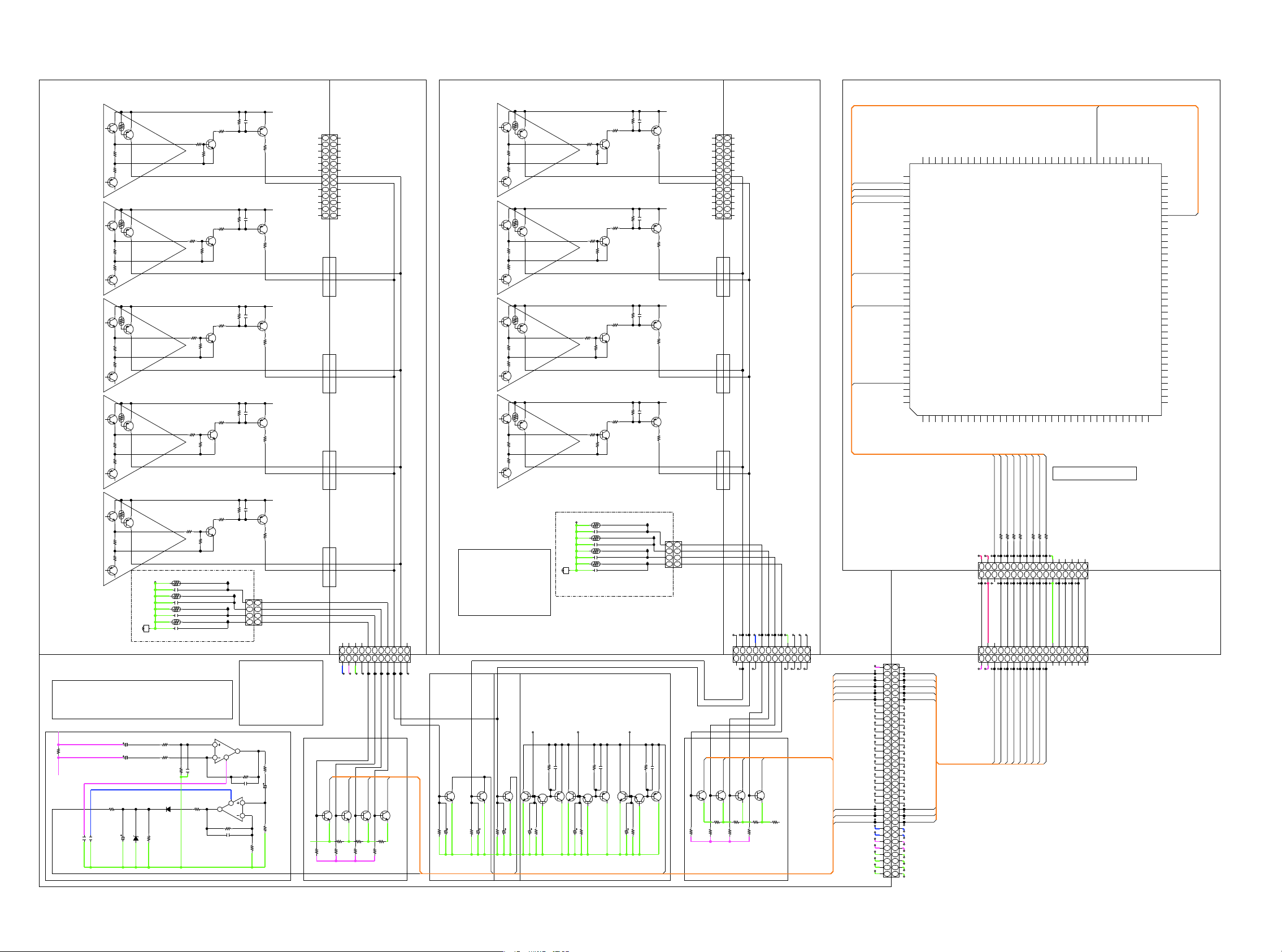
DIAGNOSTIC PATH DIAGRAM
fig.01
AVR-X5200 BLOCK DIAGRAM (A.AUDIO/Z2,3HPF)
X7200/AV8802
8ch EXT.IN
EXT-FL
FL
EXT-FR
FR
EXT-C
C
EXT-SW
T O
DIGITAL
AUDIO
BLOCK
DIAGRAN
SW
SL
SR
SBL
SBR
DAC OUT
FL
FR
C
SW1
SW2
SL
SR
SBL
SBR
FWL
FWR
FHL
FHR
ADC INPUT
MAIN AD-L
MAIN AD-R
ZONE DAC OUT
Z2DA-L
Z2DA-R
Z3DA-R
AUDIO
INPUT
GAME
CD
DVR
SAT/CBL
DVD
BD
V.AUX
PHONO
MIC
TUNER:
NA/EU/AP
ALL MODEL
AV8802
XLR
EXT-SL
EXT-SR
EXT-SBL
EXT-SBR
DA-FL
DA-FR
DA-C
DA-SW1
DA-SW2
DA-SL
DA-SR
DA-SBL
DA-SBR
DA-FWL
DA-FWR
DA-FHL
DA-FHR
(For Signal DET)
SAT/CBL
V.AUX
PHONO
TUNER
(For Zone2/3)
DA-FL/FR
GAME
CD
MP
DVD
BD
MIC
XLR
Z2L
/R
Z3L
/R
MX
XLR
V.AUX
MIC
TUNER
PHONO
DVD
SAT/CBL
GAME
CD
BD
EXT-FL/FR
MP
VOLUME IC1
(IN1L/R)
(IN2L/R)
(IN3L/R)
(IN4L/R)
(IN5L/R)
(IN6L/R)
(IN7L/R)
(IN8L/R)
(INAL/R)
(IN9L/R)
(INBL/R)
(IN10L/R)
(IN11L/R)
(IN12L/R)
(IN13L/R)
(IN14L/R)
(REC3L/R)
(ADCR)
(ADCL)
R2A15220FP
MAIN-L
MAIN-R
MAIN
(MAIN)
ZONE2
(SUB1)
Lch
2
Rch
3
H/P OUT
G
1
PREOUT
PRE_FL
PRE_FR
PRE_C
PRE_SW1
PRE_SW2
PRE_SL
PRE_SR
PRE_SBL
PRE_SBR
PRE_FWL
PRE_FWR
+
+
+
+
+
+
+
+
+
+
+
PRE_HL1
PRE_HR1
PRE_HL2
PRE_HR2
PRE_Z2L
PRE_Z2R
PRE_Z3L
PRE_Z3R
CENTER
FL
FR
SL
SR
SBL
SBR
WL
WR
HL
HR
9ch AMP SP OUT
No2
7ch
NOR
NOR
MAL
HEI
GHT
FL
FR
SL
SR
SBL
SBR
---
---
FHL
FHR
MAL
WIDE
FL
FR
SL
SR
SBL
SBR
FWL
FWR
---
---
9ch
BI-
BI-
9ch
AMP
WIR
BI-
ING
WIR
HEI
ING
GHT
WIDE
C
CCC
C
FL
FL
FL
FR
FR
FR
SL
SL
SL
SR
SR
SR
SBL
SBL
SBL
SBR
SBR
SBR
FL
FL
FL
FR
FR
FR
FHL
---
FWL
FHR
FWR
---
No6No5
7ch
+Z2
FL
FR
SL
SR
SBL
SBR
Z2L Z3L
No8CCNo7No3 No4 9oN1oN
7ch
5c
h
+Z3
+Z2
+Z3
C
---
FL
FL
---
FR
FR
---
SL
SL
---
SR
SR
---
Z2L
SBL
---
SBR
Z2R
---
---
------
---
---
------
---
Z3L
---
Z3R
---
Z3RZ2R
PRE_FL
PRE_FR
EXT-FL
(FLIN1)
DA-FL
(FLIN2)
(2chLIN)
EXT-FR
(FRIN1)
DA-FR
(FRIN2)
(2chRIN)
EXT-C
ZONE3
(SUB2)
Z2RLINE
Z2LLINE(SUBR1)
Z3LLINE
(SUBL1)
(SUBR2)
(SUBL2) Z3RLINE
MONO
HPF
MONO
HPF
MONO
HPF
MONO
HPF
DA-C
EXT-SW
DA-SW1
EXT-SW
DA-SW2
EXT-SL
DA-SL
EXT-SR
DA-SR
PRE_FL
DA-FWL
PRE_FR
DA-FWR
PRE_FL
DA-FHL
PRE_FR
DA-FHR
PRE_FL
DA-SBL
EXT-SBL
PRE_FR
DA-SBR
EXT-SBR
MONO
MONO
MONO
MONO
(SLIN1)
(SLIN2)
(SBLCIN)
(SLCIN)
(SRIN1)
(SRIN2)
(SBRCIN)
(SRCIN)
(CIN1)
(CIN2)
(SWIN1)
(SWIN2)
(SBLIN1)
(SBLIN2)
(SBLCIN)
(SLCIN)
(SBRIN1)
(SBRIN2)
(SBRCIN)
(SRCIN)
(CIN1)
(CIN2)
(SWIN1)
(SWIN2)
(SLIN1)
(SLIN2)
(SBLCIN)
(SLCIN)
(SRIN1)
(SRIN2)
(SBRCIN)
(SRCIN)
(SBLIN1)
(SBLIN2)
(SBLCIN)
(SLCIN)
(SBRIN1)
(SBRIN2)
(SBRCIN)
(SRCIN)
(FLIN1
(FLIN2)
(2chLIN)
(FRIN1)
(FRIN2)
(2chRIN)
HPF+MONO
HPF+MONO
HPF+MONO
HPF+MONO
FULL
MONO
FULL
MONO
FULL
MONO
FULL
MONO
HPF
HPF
HPF
HPF
FL
FR
C
RSV
SW1
SW2
SL
SR
FWLZ3DA-L
FWR
FHL
FHR
SBL
SBR
)
Z2L
Z2R
TONE
(FLOUT)
(FLPRE)
TONE
(FROUT)
(FRPRE)
(SLOUT)
(SLPRE)
(SROUT)
(SRPRE)
(COUT)
(SWOUT)
(SBLOUT)
(SBLPRE)
(SBROUT)
(SBRPRE)
VOLUME IC2
(COUT)
(SWOUT)
(SLOUT)
(SLPRE)
(SROUT)
(SRPRE)
(SBLOUT)
(SBLPRE)
(SBROUT)
(SBRPRE)
TONE
(FLOUT)
(FLPRE)
TONE
(FROUT)
(FRPRE)
TONE
TONE
TONE
TONE
C
R2A15220FP
ZONE2
NJW1194
ZONE3
NJW1194
PREOUT
FL
PREOUT
FR
PREOUT
C
AMPIN
PREOUT
RSV
PREOUT
SW1
PREOUT
SW2
PREOUT
SL
AMPIN
PREOUT
SR
AMPIN
PREOUT
FWL
PREOUT
FWR
PREOUT
FHL
PREOUT
FHR
PREOUT
SBL
PREOUT
SBR
PREOUT
Z2L
PREOUT
Z2R
PREOUT
Z3L
PREOUT
Z3R
HDAM AV8802
PRE_FL/FR
PRE_SL/SR
PRE_C
PRE_SW1
PRE_SW2
PRE_SBL/SBR
PRE_FHL/FHR
PRE_FWL/FWR
PRE_Z2L/Z2R
PRE_Z3L/Z3R
Z2/Z3 MONO
VOLUME
IC2
R2A15220FP
(IN1L/R)
(IN2L/R)
(IN3L/R)
(IN4L/R)
(IN5L/R)
(IN6L/R)
(IN7L/R)
(IN8L/R)
(INAL/R)
(IN9L/R)
(INBL/R)
(IN10L/R)
(IN11L/R)
(IN12L/R)
(IN13L/R)
(IN14L/R)
(REC3L/R)
ZONE3
(SUB2)
P.AMP
P.AMP
P.AMP
P.AMP
P.AMP
P.AMP
P.AMP
(SUB2L/R)
(SUB2L/R)
P.AMP
P.AMP
MAIN
ZONE2
(REC3)
(SUB1)
31
Page 32

From/To ANALOG AUDIO BLOCK DIAGRAM
fig.02a
AVR-X5200 DIGITAL AUDIO/NETWORK BLOCK DIRAGRAM
DIGITAL PCB BLOCK
Wireless Network
Input
Wired Network
Input
USB-A
Input(FRONT)
USB-A
Input(REAR)
AVR-X7200
AV8801
AVR-X5200
AVR-X7200
AV8801
Netowrk Module
CX870/CY920
iPod
Coprocessor
S.Flash
I2S_CX870/CY920
DSD_CX870/CY920
CX870/CY920_VBUclk
CX870/CY920_VBUSdata(8bit)
FCXO-05
24.576MHz
FCXO-05
25.0MHz
Ref clock Sel.
DENON Link HD
Generator Module
REFCLK
DLHD
fs Assign Sel.
DSP1 INPUT MUX
I2S_HDMIRX
DSD_HDMIRX
I2S_CX870/CY920
DSD_CX870/CY920
DIR_I2S
I2S_HDMITX
I2S_CX870/CY920
Jitter Reducer PLL
CS2100
1/2
1/4
Div.
Div.
1 2
1 2
1 2
1 2
1 2
PLLOUT
DSP1_IN_LRCK
SDRAM FLASH FLASH HSALFMARDSMARDS
1st DSP
DSP1_IN
ZONE2 I2S MUX
1
3
2
ZONE3 I2S MUX
1
3
2
SDRAM
ADSP-21487
ZONE2
Mute Logic
ZONE3
Mute Logic
2nd DSP
FLASH
Z2DAC_I2S
Z3DAC_I2S
3rd DSP
78412-PSDA78412-PSDA
DSP3 INPUT MUX
6
5
4th DSP
ADSP-21487
3
2
6
5
MAIN DAC1
PCM1690
3
2
6
5
3
2
6
5
Main ZONE
Mute Logic
1
3
2
DAC INPUT MUX
1
3
2
3
2
6
5
3
2
6
5
MAIN DAC2
PCM1690
3
2
6
5
3
2
OUTPUT
7
DA_FL
OUTPUT
1
DA_FR
OUTPUT
7
DA_C
OUTPUT
1
DA_SW1
OUTPUT
7
DA_SW2
OUTPUT
1
DA_RSV
OUTPUT
7
DA_SL
OUTPUT
1
DA_SR
OUTPUT
7
DA_SBL
OUTPUT
1
DA_SBR
OUTPUT
7
DA_FHL
OUTPUT
1
DA_FHR
OUTPUT
7
DA_FWL
OUTPUT
1
DA_FWR
Audio PLD
5M570ZF256C5N
I2S/DSD_HDMIRX
SPDIF_HDMIRX
I2S_HDMITX
SPDIF_Z2HDMI
From/To VIDEO BLOCK DIAGRAM
CX870/CY920_VBUclk
CX870/CY920_VBUSdata(8bit)
OPT1
OPT2
COAX1
COAX2
DENONLinkHD
AVR-X5200
INPUT
INPUT
OUTPUT
INPUT
OUTPUT
OUTPUT
I2S/DSD_HDMIRX
I2S_HDMITX
CX870/CY920_VBUclk
CX870/CY920_VBUSdata(8bit)
SPDIF_HDMIRX
SPDIF_Z2HDMI
COAX1
COAX2
OPT1
OPT2
SPDIF_HDMIRX
Main DIR
PCM9211
ADCCLK
SDATA
Z2_SPDIF
MAIN ADC
AK5358B
FIDPS_3ZIMDH2Z_FIDPS
ZONE2 DAC
PCM5100
INPUT
ADIN_FL
INPUT
ADIN_FR
OUTPUT
Z2DA_L
OUTPUT
Z2DA_R
OPT1
OPT2
COAX1
COAX2
Z2_SPDIF
ZONE2 DI
LC89091
R
JH
Z2DIR_I2S
ZONE2 DAC
PCM5100
OUTPUT
Z3DA_L
OUTPUT
Z3DA_R
DLHD
AVR-X5200
AVR-X7200
Z3_SPDIF
ZONE3 DIR
Z3DIR_I2S
LC89091JH
32
Page 33

fig.02b
AVR-X5200 BLOCK DIAGRAM (A.AUDIO/Z2,3HPF)
X7200/AV8802
T O
DIGITAL
AUDIO
BLOCK
DIAGRAN
8ch EXT.IN
FL
FR
C
SW
SL
SR
SBL
SBR
DAC OUT
FL
FR
C
SW1
SW2
SL
SR
SBL
SBR
FWL
FWR
FHL
FHR
ADC INPUT
MAIN AD-L
MAIN AD-R
ZONE DAC OUT
Z2DA-L
Z2DA-R
Z3DA-R
AUDIO
INPUT
GAME
CD
DVR
SAT/CBL
DVD
BD
V.AUX
PHONO
MIC
TUNER:
NA/EU/AP
ALL MODEL
AV8802
XLR
EXT-FL
EXT-FR
EXT-C
EXT-SW
EXT-SL
EXT-SR
EXT-SBL
EXT-SBR
DA-FL
DA-FR
DA-C
DA-SW1
DA-SW2
DA-SL
DA-SR
DA-SBL
DA-SBR
DA-FWL
DA-FWR
DA-FHL
DA-FHR
(For Signal DET)
GAME
SAT/CBL
V.AUX
PHONO
TUNER
(For Zone2/3)
DA-FL/FR
Z2L
/R
Z3L
/R
MX
XLR
V.AUX
MIC
TUNER
PHONO
DVD
SAT/CBL
GAME
CD
BD
EXT-FL/FR
MP
CD
MP
DVD
BD
MIC
XLR
VOLUME IC1
R2A15220FP
MAIN
(MAIN)
(IN1L/R)
(IN2L/R)
(IN3L/R)
(IN4L/R)
(IN5L/R)
(IN6L/R)
(IN7L/R)
(IN8L/R)
(INAL/R)
(IN9L/R)
(INBL/R)
(IN10L/R)
(IN11L/R)
(IN12L/R)
(IN13L/R)
(IN14L/R)
(REC3L/R)
MAIN-L
(ADCR)
MAIN-R
(ADCL)
ZONE2
(SUB1)
ZONE3
(SUB2)
Z2RLINE
Z2LLINE(SUBR1)
(SUBL1)
Z3LLINE
(SUBR2)
MONO
HPF
MONO
HPF
MONO
HPF
MONO
HPF
PRE_FL
PRE_FR
EXT-FL
(FLIN1)
DA-FL
(FLIN2)
(2chLIN)
EXT-FR
(FRIN1)
DA-FR
(FRIN2)
(2chRIN)
EXT-C
(SLIN1)
DA-C
(SLIN2)
(SBLCIN)
(SLCIN)
(SRIN1)
(SRIN2)
(SBRCIN)
(SRCIN)
EXT-SW
(CIN1)
DA-SW1
(CIN2)
EXT-SW
(SWIN1)
DA-SW2
(SWIN2)
EXT-SL
(SBLIN1)
DA-SL
(SBLIN2)
(SBLCIN)
(SLCIN)
EXT-SR
(SBRIN1)
DA-SR
(SBRIN2)
(SBRCIN)
PRE_FL
DA-FWL
PRE_FR
DA-FWR
PRE_FL
DA-FHL
PRE_FR
DA-FHR
PRE_FL
DA-SBL
EXT-SBL
PRE_FR
DA-SBR
EXT-SBR
MONO
MONO
MONO
MONO
(SRCIN)
(CIN1)
(CIN2)
(SWIN1)
(SWIN2)
(SLIN1)
(SLIN2)
(SBLCIN)
(SLCIN)
(SRIN1)
(SRIN2)
(SBRCIN)
(SRCIN)
(SBLIN1)
(SBLIN2)
(SBLCIN)
(SLCIN)
(SBRIN1)
(SBRIN2)
(SBRCIN)
(SRCIN)
(FLIN1
(FLIN2)
(2chLIN)
(FRIN1)
(FRIN2)
(2chRIN)
HPF+MONO
HPF+MONO
HPF+MONO
HPF+MONO
FULL
MONO
FULL
MONO
FULL
MONO
FULL
MONO
HPF
HPF
HPF
HPF
(SUBL2) Z3RLINE
FL
FR
C
RSV
SW1
SW2
SL
SR
FWLZ3DA-L
FWR
FHL
FHR
SBL
SBR
)
Z2L
Z2R
TONE
(FLOUT)
(FLPRE)
TONE
(FROUT)
(FRPRE)
(SLOUT)
(SLPRE)
(SROUT)
(SRPRE)
(COUT)
(SWOUT)
(SBLOUT)
(SBLPRE)
(SBROUT)
(SBRPRE)
VOLUME IC2
(COUT)
(SWOUT)
(SLOUT)
(SLPRE)
(SROUT)
(SRPRE)
(SBLOUT)
(SBLPRE)
(SBROUT)
(SBRPRE)
TONE
(FLOUT)
(FLPRE)
TONE
(FROUT)
(FRPRE)
TONE
TONE
TONE
TONE
C
R2A15220FP
ZONE2
NJW1194
ZONE3
NJW1194
PREOUT
FL
PREOUT
FR
PREOUT
C
AMPIN
PREOUT
RSV
PREOUT
SW1
PREOUT
SW2
PREOUT
SL
AMPIN
PREOUT
SR
AMPIN
PREOUT
FWL
PREOUT
FWR
PREOUT
FHL
PREOUT
FHR
PREOUT
SBL
PREOUT
SBR
PREOUT
Z2L
PREOUT
Z2R
PREOUT
Z3L
PREOUT
Z3R
HDAM AV8802
PRE_FL/FR
PRE_SL/SR
PRE_C
PRE_SW1
PRE_SW2
PRE_SBL/SBR
PRE_FHL/FHR
PRE_FWL/FWR
PRE_Z2L/Z2R
PRE_Z3L/Z3R
Z2/Z3 MONO
VOLUME
IC2
R2A15220FP
(IN1L/R)
(IN2L/R)
(IN3L/R)
(IN4L/R)
(IN5L/R)
(IN6L/R)
(IN7L/R)
(IN8L/R)
(INAL/R)
(IN9L/R)
(INBL/R)
(IN10L/R)
(IN11L/R)
(IN12L/R)
(IN13L/R)
(IN14L/R)
(REC3L/R)
ZONE3
(SUB2)
Lch
2
Rch
3
1
H/P OUT
G
PREOUT
PRE_FL
PRE_FR
PRE_C
PRE_SW1
PRE_SW2
PRE_SL
PRE_SR
PRE_SBL
PRE_SBR
PRE_FWL
PRE_FWR
PRE_HL1
PRE_HR1
PRE_HL2
PRE_HR2
9ch AMP SP OUT
No6No5
No2
7ch
NOR
P.AMP
P.AMP
P.AMP
P.AMP
P.AMP
+
+
+
PRE_Z2L
PRE_Z2R
PRE_Z3L
PRE_Z3R
CENTER
FL
FR
+
+
NOR
MAL
HEI
GHT
FL
FR
SL
SR
SL
SR
MAL
WIDE
FL
FR
SL
SR
9ch
BI-
BI-
9ch
AMP
WIR
BI-
ING
WIR
HEI
ING
GHT
WIDE
C
CCC
C
FL
FL
FL
FR
FR
FR
SL
SL
SL
SR
SR
SR
P.AMP
P.AMP
SBL
+
SBR
(SUB2L/R)
(SUB2L/R)
P.AMP
P.AMP
MAIN
ZONE2
(REC3)
(SUB1)
+
WL
+
WR
+
SBL
SBR
---
---
FHL
FHR
HL
+
HR
+
SBL
SBL
SBL
SBL
SBR
SBR
SBR
SBR
FL
FL
FL
FWL
FR
FR
FR
FWR
---
FHL
---
FWL
---
FHR
FWR
---
7ch
7ch
+Z3
+Z2
FL
FR
SL
SR
SBL
SBL
SBR
SBR
------
------
Z2L Z3L
Z3RZ2R
No8CCNo7No3 No4 9oN1oN
5c
h
+Z2
+Z3
C
---
FL
FL
---
FR
FR
---
SL
SL
---
SR
SR
---
Z2L
---
Z2R
---
---
---
---
---
Z3L
---
Z3R
---
33
Page 34

fig.03a
HDMI
HDMI 1
INPUT
HDMI
HDMI 2
INPUT
HDMI
HDMI 3
INPUT
HDMI
HDMI 4
INPUT
HDMI
HDMI 5
INPUT
HDMI
HDMI 6
INPUT
HDMI
HDMI 7
INPUT
HDMI
FRONT
INPUT
DIGITAL AUDIO / NETWORK BLOCK
FROM
DIAGRAM
CX870/CY920_VBUSclk
CX870/CY920_VBUSdata(8bit)
AVR-X5200 BLOCK DIAGRAM (VIDEO)
-
-
-
-
-
-
-
-
AVDM2000
DEC. Select
6dB
Y_OUT4
10
DIGITAL PCB BLOCK
TMDS
330
TMDS
TMDS
TMDS
TMDS
TMDS
TMDS
TMDS
RX3
RX2
RX1
RX0
330
330
330
DEC Y
DEC Cb
150
150
470
470
Matlix SW
Rx
MN864778
HDMI
buffer
AD8195
VIDEO
DECODER
ADV7850
DEC Cr
150
470
TX1
TMDS
TX0
RX3
RX2
RX1
RX0
Matlix SW
Rx
MN864778
TX0
TX1
TMDS
TMDS
TMDS
TMDS
DEC V
150470
RX1
RX0
RX3
TTL
S.FLASH
128Mbit
Z2 SPDIF
TX1
HDMI Tx
scaler
MN864777
TX0
RX2
-
-
-
-
-
-
-
-
TO D.AUDIO (SPDIF)
TMDS
TMDS
ARC
TMDS
TO D.AUDIO (I2S/DSD)
TO D.AUDIO (SPDIF)
FROM D.AUDIO (I2S)
HDMI 3
HDMI 1
HDMI 2
-
HDMI
MONITOR1
ZONE2
HDMI
MONITOR1
ZONE1
HDMI
MONITOR2
ZONE1
-
-
-
SPDIF_Z2HDMI
I2S/DSD_HDMIRX
SPDIF_HDMIRX
I2S_HDMITX
TO
DIGITAL AUDIO
BLOCK DIAGRAM
FROM
DIGITAL AUDIO/NETWORK
BLOCK DIAGRAM
TTL
VIDEO
PLD
5M570Z
TTL
scaler
GUI
ADV8003
DDR2
DDR2
COMPONENT
INPUT1
COMPONENT
INPUT2
COMPONENT
INPUT3
BD_Y
DVD_Y
SAT_Y
Y
Cb
BD
Cr
Y
Cb
DVD
Cr
Y
Cb
SAT
Cr
75
75
75
75
75
75
75
75
75
BD_Y
BD_Cb
BD_Cr
DVD_Y
DVD_Cb
DVD_Cr
SAT_Y
SAT_Cb
SAT_Cr
BD_Cb
DVD_Cb
SAT_Cb
BD_Cr
DVD_Cr
SAT_Cr
Y_IN1
Y_IN2
Y_IN3
Y_IN4
Y_IN5
Y_IN6
Cb_IN1
Cb_IN2
Cb_IN3
Cb_IN4
Cb_IN5
Cb_IN6
Cr_IN1
Cr_IN2
Cr_IN3
Cr_IN4
Cr_IN5
Cr_IN6
Zone1 Select
6dB
Zone2 Select
6dB
DEC. Select
6dB
ZoNE1 Select
6dB
Zone2 Select
6dB
DEC. Select
6dB
ZoNE1 Select
6dB
Zone2 Select
6dB
Y_OUT2
Y_OUT1
CB_OUT4
CB_OUT2
CB_OUT1
CR_OUT4
CR_OUT2
CR_OUT1
10
75
10
75
75
75
75
75
Y
COMPONENT
Cb
MONITOR
ZONE1
Cr
COMPONENT
CbYMONITOR
ZONE2
Cr
AVR-X7200,AV8802 only
COMPOSITE
INPUT
COMPOSITE
INPUT
COMPOSITE
INPUT
COMPOSITE
INPUT
COMPOSITE
INPUT
SAT
DVD
GAME
Blu-ray
V.AUX
Z1 V Select
6dB
V_OUT1
75
75
75
75
75
SAT_V
DVD_V
GAME_V
Blu-ray_V
VAUX_V
DVD_V
SAT_V
GAME_V
VAUX_V
Blu-ray_V
V_IN2
V_IN3
V_IN
V_IN6
V_IN7
V_IN1
V_IN5
V_IN8
V_IN9
4
Z2 V Select
6dB
DEC V Select
6dB
V_OUT2
V_OUT4
10
75
75
CVBS
MONITOR
ZONE1
CVBS
MONITOR
ZONE2
34
Page 35

fig.03b
AVR-X5200 DIGITAL AUDIO/NETWORK BLOCK DIRAGRAM
DIGITAL PCB BLOCK
Wireless Network
Input
Wired Network
Input
USB-A
Input(FRONT)
USB-A
Input(REAR)
AVR-X7200
AV8801
AVR-X5200
AVR-X7200
AV8801
Netowrk Module
CX870/CY920
iPod
Coprocessor
S.Flash
I2S_CX870/CY920
DSD_CX870/CY920
CX870/CY920_VBUclk
CX870/CY920_VBUSdata(8bit)
FCXO-05
24.576MHz
FCXO-05
25.0MHz
Ref clock Sel.
DENON Link HD
Generator Module
REFCLK
DLHD
fs Assign Sel.
DSP1 INPUT MUX
I2S_HDMIRX
DSD_HDMIRX
I2S_CX870/CY920
DSD_CX870/CY920
DIR_I2S
I2S_HDMITX
I2S_CX870/CY920
Jitter Reducer PLL
CS2100
1/2
1/4
Div.
Div.
1 2
1 2
1 2
1 2
1 2
PLLOUT
DSP1_IN_LRCK
SDRAM FLASH FLASH HSALFMARDSMARDS
1st DSP
DSP1_IN
ZONE2 I2S MUX
1
3
2
ZONE3 I2S MUX
1
3
2
SDRAM
ADSP-21487
ZONE2
Mute Logic
ZONE3
Mute Logic
2nd DSP
FLASH
Z2DAC_I2S
Z3DAC_I2S
3rd DSP
78412-PSDA78412-PSDA
DSP3 INPUT MUX
6
5
4th DSP
ADSP-21487
3
2
6
5
MAIN DAC1
PCM1690
3
2
6
5
3
2
6
5
Main ZONE
Mute Logic
1
3
2
DAC INPUT MUX
1
3
2
3
2
6
5
3
2
6
5
MAIN DAC2
PCM1690
3
2
6
5
3
2
OUTPUT
7
DA_FL
OUTPUT
1
DA_FR
OUTPUT
7
DA_C
OUTPUT
1
DA_SW1
OUTPUT
7
DA_SW2
OUTPUT
1
DA_RSV
OUTPUT
7
DA_SL
OUTPUT
1
DA_SR
OUTPUT
7
DA_SBL
OUTPUT
1
DA_SBR
OUTPUT
7
DA_FHL
OUTPUT
1
DA_FHR
OUTPUT
7
DA_FWL
From/To ANALOG AUDIO BLOCK DIAGRAM
OUTPUT
1
DA_FWR
Audio PLD
5M570ZF256C5N
I2S/DSD_HDMIRX
SPDIF_HDMIRX
I2S_HDMITX
SPDIF_Z2HDMI
From/To VIDEO BLOCK DIAGRAM
CX870/CY920_VBUclk
CX870/CY920_VBUSdata(8bit)
OPT1
OPT2
COAX1
COAX2
DENONLinkHD
AVR-X5200
INPUT
INPUT
OUTPUT
INPUT
OUTPUT
OUTPUT
I2S/DSD_HDMIRX
I2S_HDMITX
CX870/CY920_VBUclk
CX870/CY920_VBUSdata(8bit)
SPDIF_HDMIRX
SPDIF_Z2HDMI
COAX1
COAX2
OPT1
OPT2
SPDIF_HDMIRX
Main DIR
PCM9211
ADCCLK
SDATA
Z2_SPDIF
MAIN ADC
AK5358B
FIDPS_3ZIMDH2Z_FIDPS
ZONE2 DAC
PCM5100
INPUT
ADIN_FL
INPUT
ADIN_FR
OUTPUT
Z2DA_L
OUTPUT
Z2DA_R
OPT1
OPT2
COAX1
COAX2
Z2_SPDIF
ZONE2 DI
LC89091
R
JH
Z2DIR_I2S
ZONE2 DAC
PCM5100
OUTPUT
Z3DA_L
OUTPUT
Z3DA_R
DLHD
AVR-X5200
AVR-X7200
Z3_SPDIF
ZONE3 DIR
Z3DIR_I2S
LC89091JH
35
Page 36

fig.03c
AVR-X5200 BLOCK DIAGRAM (A.AUDIO/Z2,3HPF)
X7200/AV8802
T O
DIGITAL
AUDIO
BLOCK
DIAGRAN
8ch EXT.IN
FL
FR
C
SW
SL
SR
SBL
SBR
DAC OUT
FL
FR
C
SW1
SW2
SL
SR
SBL
SBR
FWL
FWR
FHL
FHR
ADC INPUT
MAIN AD-L
MAIN AD-R
ZONE DAC OUT
Z2DA-L
Z2DA-R
Z3DA-R
AUDIO
INPUT
GAME
CD
DVR
SAT/CBL
DVD
BD
V.AUX
PHONO
MIC
TUNER:
NA/EU/AP
ALL MODEL
AV8802
XLR
EXT-FL
EXT-FR
EXT-C
EXT-SW
EXT-SL
EXT-SR
EXT-SBL
EXT-SBR
DA-FL
DA-FR
DA-C
DA-SW1
DA-SW2
DA-SL
DA-SR
DA-SBL
DA-SBR
DA-FWL
DA-FWR
DA-FHL
DA-FHR
(For Signal DET)
GAME
SAT/CBL
V.AUX
PHONO
TUNER
(For Zone2/3)
DA-FL/FR
Z2L
/R
Z3L
/R
MX
XLR
V.AUX
MIC
TUNER
PHONO
DVD
SAT/CBL
GAME
CD
BD
EXT-FL/FR
MP
CD
MP
DVD
BD
MIC
XLR
VOLUME IC1
R2A15220FP
MAIN
(MAIN)
(IN1L/R)
(IN2L/R)
(IN3L/R)
(IN4L/R)
(IN5L/R)
(IN6L/R)
(IN7L/R)
(IN8L/R)
(INAL/R)
(IN9L/R)
(INBL/R)
(IN10L/R)
(IN11L/R)
(IN12L/R)
(IN13L/R)
(IN14L/R)
(REC3L/R)
MAIN-L
(ADCR)
MAIN-R
(ADCL)
ZONE2
(SUB1)
ZONE3
(SUB2)
Z2RLINE
Z2LLINE(SUBR1)
(SUBL1)
Z3LLINE
(SUBR2)
MONO
HPF
MONO
HPF
MONO
HPF
MONO
HPF
PRE_FL
PRE_FR
EXT-FL
(FLIN1)
DA-FL
(FLIN2)
(2chLIN)
EXT-FR
(FRIN1)
DA-FR
(FRIN2)
(2chRIN)
EXT-C
(SLIN1)
DA-C
(SLIN2)
(SBLCIN)
(SLCIN)
(SRIN1)
(SRIN2)
(SBRCIN)
(SRCIN)
EXT-SW
(CIN1)
DA-SW1
(CIN2)
EXT-SW
(SWIN1)
DA-SW2
(SWIN2)
EXT-SL
(SBLIN1)
DA-SL
(SBLIN2)
(SBLCIN)
(SLCIN)
EXT-SR
(SBRIN1)
DA-SR
(SBRIN2)
(SBRCIN)
PRE_FL
DA-FWL
PRE_FR
DA-FWR
PRE_FL
DA-FHL
PRE_FR
DA-FHR
PRE_FL
DA-SBL
EXT-SBL
PRE_FR
DA-SBR
EXT-SBR
MONO
MONO
MONO
MONO
(SRCIN)
(CIN1)
(CIN2)
(SWIN1)
(SWIN2)
(SLIN1)
(SLIN2)
(SBLCIN)
(SLCIN)
(SRIN1)
(SRIN2)
(SBRCIN)
(SRCIN)
(SBLIN1)
(SBLIN2)
(SBLCIN)
(SLCIN)
(SBRIN1)
(SBRIN2)
(SBRCIN)
(SRCIN)
(FLIN1
(FLIN2)
(2chLIN)
(FRIN1)
(FRIN2)
(2chRIN)
HPF+MONO
HPF+MONO
HPF+MONO
HPF+MONO
FULL
MONO
FULL
MONO
FULL
MONO
FULL
MONO
HPF
HPF
HPF
HPF
(SUBL2) Z3RLINE
FL
FR
C
RSV
SW1
SW2
SL
SR
FWLZ3DA-L
FWR
FHL
FHR
SBL
SBR
)
Z2L
Z2R
TONE
(FLOUT)
(FLPRE)
TONE
(FROUT)
(FRPRE)
(SLOUT)
(SLPRE)
(SROUT)
(SRPRE)
(COUT)
(SWOUT)
(SBLOUT)
(SBLPRE)
(SBROUT)
(SBRPRE)
VOLUME IC2
(COUT)
(SWOUT)
(SLOUT)
(SLPRE)
(SROUT)
(SRPRE)
(SBLOUT)
(SBLPRE)
(SBROUT)
(SBRPRE)
TONE
(FLOUT)
(FLPRE)
TONE
(FROUT)
(FRPRE)
TONE
TONE
TONE
TONE
C
R2A15220FP
ZONE2
NJW1194
ZONE3
NJW1194
PREOUT
FL
PREOUT
FR
PREOUT
C
AMPIN
PREOUT
RSV
PREOUT
SW1
PREOUT
SW2
PREOUT
SL
AMPIN
PREOUT
SR
AMPIN
PREOUT
FWL
PREOUT
FWR
PREOUT
FHL
PREOUT
FHR
PREOUT
SBL
PREOUT
SBR
PREOUT
Z2L
PREOUT
Z2R
PREOUT
Z3L
PREOUT
Z3R
HDAM AV8802
PRE_FL/FR
PRE_SL/SR
PRE_C
PRE_SW1
PRE_SW2
PRE_SBL/SBR
PRE_FHL/FHR
PRE_FWL/FWR
PRE_Z2L/Z2R
PRE_Z3L/Z3R
Z2/Z3 MONO
VOLUME
IC2
R2A15220FP
(IN1L/R)
(IN2L/R)
(IN3L/R)
(IN4L/R)
(IN5L/R)
(IN6L/R)
(IN7L/R)
(IN8L/R)
(INAL/R)
(IN9L/R)
(INBL/R)
(IN10L/R)
(IN11L/R)
(IN12L/R)
(IN13L/R)
(IN14L/R)
(REC3L/R)
ZONE3
(SUB2)
Lch
2
Rch
3
1
H/P OUT
G
PREOUT
PRE_FL
PRE_FR
PRE_C
PRE_SW1
PRE_SW2
PRE_SL
PRE_SR
PRE_SBL
PRE_SBR
PRE_FWL
PRE_FWR
PRE_HL1
PRE_HR1
PRE_HL2
PRE_HR2
9ch AMP SP OUT
No6No5
No2
7ch
NOR
P.AMP
P.AMP
P.AMP
P.AMP
P.AMP
+
+
+
PRE_Z2L
PRE_Z2R
PRE_Z3L
PRE_Z3R
CENTER
FL
FR
+
+
NOR
MAL
HEI
GHT
FL
FR
SL
SR
SL
SR
MAL
WIDE
FL
FR
SL
SR
9ch
BI-
BI-
9ch
AMP
WIR
BI-
ING
WIR
HEI
ING
GHT
WIDE
C
CCC
C
FL
FL
FL
FR
FR
FR
SL
SL
SL
SR
SR
SR
P.AMP
P.AMP
SBL
+
SBR
(SUB2L/R)
(SUB2L/R)
P.AMP
P.AMP
MAIN
ZONE2
(REC3)
(SUB1)
+
WL
+
WR
+
SBL
SBR
---
---
FHL
FHR
HL
+
HR
+
SBL
SBL
SBL
SBL
SBR
SBR
SBR
SBR
FL
FL
FL
FWL
FR
FR
FR
FWR
---
FHL
---
FWL
---
FHR
FWR
---
7ch
+Z2
FL
FR
SL
SR
SBL
SBR
Z2L Z3L
No8CCNo7No3 No4 9oN1oN
7ch
5c
h
+Z3
+Z2
+Z3
C
---
FL
FL
---
FR
FR
---
SL
SL
---
SR
SR
---
Z2L
SBL
---
SBR
Z2R
---
---
------
---
---
------
---
Z3L
---
Z3R
---
Z3RZ2R
36
Page 37

fig.04a
AVR-X5200 DIGITAL AUDIO/NETWORK BLOCK DIRAGRAM
DIGITAL PCB BLOCK
Wireless Network
Input
Wired Network
Input
USB-A
Input(FRONT)
USB-A
Input(REAR)
AVR-X7200
AV8801
AVR-X5200
AVR-X7200
AV8801
Netowrk Module
CX870/CY920
iPod
Coprocessor
S.Flash
I2S_CX870/CY920
DSD_CX870/CY920
CX870/CY920_VBUclk
CX870/CY920_VBUSdata(8bit)
FCXO-05
24.576MHz
FCXO-05
25.0MHz
Ref clock Sel.
DENON Link HD
Generator Module
REFCLK
DLHD
fs Assign Sel.
DSP1 INPUT MUX
I2S_HDMIRX
DSD_HDMIRX
I2S_CX870/CY920
DSD_CX870/CY920
DIR_I2S
I2S_HDMITX
I2S_CX870/CY920
Jitter Reducer PLL
CS2100
1/2
1/4
Div.
Div.
1 2
1 2
1 2
1 2
1 2
PLLOUT
DSP1_IN_LRCK
SDRAM FLASH FLASH HSALFMARDSMARDS
1st DSP
DSP1_IN
ZONE2 I2S MUX
1
3
2
ZONE3 I2S MUX
1
3
2
SDRAM
ADSP-21487
ZONE2
Mute Logic
ZONE3
Mute Logic
2nd DSP
FLASH
Z2DAC_I2S
Z3DAC_I2S
3rd DSP
78412-PSDA78412-PSDA
DSP3 INPUT MUX
6
5
4th DSP
ADSP-21487
3
2
6
5
MAIN DAC1
PCM1690
3
2
6
5
3
2
6
5
Main ZONE
Mute Logic
1
3
2
DAC INPUT MUX
1
3
2
3
2
6
5
3
2
6
5
MAIN DAC2
PCM1690
3
2
6
5
3
2
OUTPUT
7
DA_FL
OUTPUT
1
DA_FR
OUTPUT
7
DA_C
OUTPUT
1
DA_SW1
OUTPUT
7
DA_SW2
OUTPUT
1
DA_RSV
OUTPUT
7
DA_SL
OUTPUT
1
DA_SR
OUTPUT
7
DA_SBL
OUTPUT
1
DA_SBR
OUTPUT
7
DA_FHL
OUTPUT
1
DA_FHR
OUTPUT
7
DA_FWL
From/To ANALOG AUDIO BLOCK DIAGRAM
OUTPUT
1
DA_FWR
Audio PLD
5M570ZF256C5N
I2S/DSD_HDMIRX
SPDIF_HDMIRX
I2S_HDMITX
SPDIF_Z2HDMI
From/To VIDEO BLOCK DIAGRAM
CX870/CY920_VBUclk
CX870/CY920_VBUSdata(8bit)
OPT1
OPT2
COAX1
COAX2
DENONLinkHD
AVR-X5200
INPUT
INPUT
OUTPUT
INPUT
OUTPUT
OUTPUT
I2S/DSD_HDMIRX
I2S_HDMITX
CX870/CY920_VBUclk
CX870/CY920_VBUSdata(8bit)
SPDIF_HDMIRX
SPDIF_Z2HDMI
COAX1
COAX2
OPT1
OPT2
SPDIF_HDMIRX
Main DIR
PCM9211
ADCCLK
SDATA
Z2_SPDIF
MAIN ADC
AK5358B
FIDPS_3ZIMDH2Z_FIDPS
ZONE2 DAC
PCM5100
INPUT
ADIN_FL
INPUT
ADIN_FR
OUTPUT
Z2DA_L
OUTPUT
Z2DA_R
OPT1
OPT2
COAX1
COAX2
Z2_SPDIF
ZONE2 DI
LC89091JH
R
Z2DIR_I2S
ZONE2 DAC
PCM5100
OUTPUT
Z3DA_L
OUTPUT
Z3DA_R
DLHD
AVR-X5200
AVR-X7200
Z3_SPDIF
ZONE3 DIR
Z3DIR_I2S
LC89091JH
37
Page 38

fig.04b
AVR-X5200 BLOCK DIAGRAM (A.AUDIO/Z2,3HPF)
X7200/AV8802
T O
DIGITAL
AUDIO
BLOCK
DIAGRAN
8ch EXT.IN
FL
FR
C
SW
SL
SR
SBL
SBR
DAC OUT
FL
FR
C
SW1
SW2
SL
SR
SBL
SBR
FWL
FWR
FHL
FHR
ADC INPUT
MAIN AD-L
MAIN AD-R
ZONE DAC OUT
Z2DA-L
Z2DA-R
Z3DA-R
AUDIO
INPUT
GAME
CD
DVR
SAT/CBL
DVD
BD
V.AUX
PHONO
MIC
TUNER:
NA/EU/AP
ALL MODEL
AV8802
XLR
EXT-FL
EXT-FR
EXT-C
EXT-SW
EXT-SL
EXT-SR
EXT-SBL
EXT-SBR
DA-FL
DA-FR
DA-C
DA-SW1
DA-SW2
DA-SL
DA-SR
DA-SBL
DA-SBR
DA-FWL
DA-FWR
DA-FHL
DA-FHR
(For Signal DET)
GAME
SAT/CBL
V.AUX
PHONO
TUNER
(For Zone2/3)
DA-FL/FR
Z2L
/R
Z3L
/R
MX
XLR
V.AUX
MIC
TUNER
PHONO
DVD
SAT/CBL
GAME
CD
BD
EXT-FL/FR
MP
CD
MP
DVD
BD
MIC
XLR
VOLUME IC1
R2A15220FP
MAIN
(MAIN)
(IN1L/R)
(IN2L/R)
(IN3L/R)
(IN4L/R)
(IN5L/R)
(IN6L/R)
(IN7L/R)
(IN8L/R)
(INAL/R)
(IN9L/R)
(INBL/R)
(IN10L/R)
(IN11L/R)
(IN12L/R)
(IN13L/R)
(IN14L/R)
(REC3L/R)
MAIN-L
(ADCR)
MAIN-R
(ADCL)
ZONE2
(SUB1)
ZONE3
(SUB2)
Z2RLINE
Z2LLINE(SUBR1)
(SUBL1)
Z3LLINE
(SUBR2)
MONO
HPF
MONO
HPF
MONO
HPF
MONO
HPF
PRE_FL
PRE_FR
EXT-FL
(FLIN1)
DA-FL
(FLIN2)
(2chLIN)
EXT-FR
(FRIN1)
DA-FR
(FRIN2)
(2chRIN)
EXT-C
(SLIN1)
DA-C
(SLIN2)
(SBLCIN)
(SLCIN)
(SRIN1)
(SRIN2)
(SBRCIN)
(SRCIN)
EXT-SW
(CIN1)
DA-SW1
(CIN2)
EXT-SW
(SWIN1)
DA-SW2
(SWIN2)
EXT-SL
(SBLIN1)
DA-SL
(SBLIN2)
(SBLCIN)
(SLCIN)
EXT-SR
(SBRIN1)
DA-SR
(SBRIN2)
(SBRCIN)
PRE_FL
DA-FWL
PRE_FR
DA-FWR
PRE_FL
DA-FHL
PRE_FR
DA-FHR
PRE_FL
DA-SBL
EXT-SBL
PRE_FR
DA-SBR
EXT-SBR
MONO
MONO
MONO
MONO
(SRCIN)
(CIN1)
(CIN2)
(SWIN1)
(SWIN2)
(SLIN1)
(SLIN2)
(SBLCIN)
(SLCIN)
(SRIN1)
(SRIN2)
(SBRCIN)
(SRCIN)
(SBLIN1)
(SBLIN2)
(SBLCIN)
(SLCIN)
(SBRIN1)
(SBRIN2)
(SBRCIN)
(SRCIN)
(FLIN1
(FLIN2)
(2chLIN)
(FRIN1)
(FRIN2)
(2chRIN)
HPF+MONO
HPF+MONO
HPF+MONO
HPF+MONO
FULL
MONO
FULL
MONO
FULL
MONO
FULL
MONO
HPF
HPF
HPF
HPF
(SUBL2) Z3RLINE
FL
FR
C
RSV
SW1
SW2
SL
SR
FWLZ3DA-L
FWR
FHL
FHR
SBL
SBR
)
Z2L
Z2R
TONE
(FLOUT)
(FLPRE)
TONE
(FROUT)
(FRPRE)
(SLOUT)
(SLPRE)
(SROUT)
(SRPRE)
(COUT)
(SWOUT)
(SBLOUT)
(SBLPRE)
(SBROUT)
(SBRPRE)
VOLUME IC2
(COUT)
(SWOUT)
(SLOUT)
(SLPRE)
(SROUT)
(SRPRE)
(SBLOUT)
(SBLPRE)
(SBROUT)
(SBRPRE)
TONE
(FLOUT)
(FLPRE)
TONE
(FROUT)
(FRPRE)
TONE
TONE
TONE
TONE
C
R2A15220FP
ZONE2
NJW1194
ZONE3
NJW1194
PREOUT
FL
PREOUT
FR
PREOUT
C
AMPIN
PREOUT
RSV
PREOUT
SW1
PREOUT
SW2
PREOUT
SL
AMPIN
PREOUT
SR
AMPIN
PREOUT
FWL
PREOUT
FWR
PREOUT
FHL
PREOUT
FHR
PREOUT
SBL
PREOUT
SBR
PREOUT
Z2L
PREOUT
Z2R
PREOUT
Z3L
PREOUT
Z3R
HDAM AV8802
PRE_FL/FR
PRE_SL/SR
PRE_C
PRE_SW1
PRE_SW2
PRE_SBL/SBR
PRE_FHL/FHR
PRE_FWL/FWR
PRE_Z2L/Z2R
PRE_Z3L/Z3R
Z2/Z3 MONO
VOLUME
IC2
R2A15220FP
(IN1L/R)
(IN2L/R)
(IN3L/R)
(IN4L/R)
(IN5L/R)
(IN6L/R)
(IN7L/R)
(IN8L/R)
(INAL/R)
(IN9L/R)
(INBL/R)
(IN10L/R)
(IN11L/R)
(IN12L/R)
(IN13L/R)
(IN14L/R)
(REC3L/R)
ZONE3
(SUB2)
Lch
2
Rch
3
1
H/P OUT
G
PREOUT
PRE_FL
PRE_FR
PRE_C
PRE_SW1
PRE_SW2
PRE_SL
PRE_SR
PRE_SBL
PRE_SBR
PRE_FWL
PRE_FWR
PRE_HL1
PRE_HR1
PRE_HL2
PRE_HR2
9ch AMP SP OUT
No6No5
No2
7ch
NOR
P.AMP
P.AMP
P.AMP
P.AMP
P.AMP
+
+
+
PRE_Z2L
PRE_Z2R
PRE_Z3L
PRE_Z3R
CENTER
FL
FR
+
+
NOR
MAL
HEI
GHT
FL
FR
SL
SR
SL
SR
MAL
WIDE
FL
FR
SL
SR
9ch
BI-
BI-
9ch
AMP
WIR
BI-
ING
WIR
HEI
ING
GHT
WIDE
C
CCC
C
FL
FL
FL
FR
FR
FR
SL
SL
SL
SR
SR
SR
P.AMP
P.AMP
SBL
+
SBR
(SUB2L/R)
(SUB2L/R)
P.AMP
P.AMP
MAIN
ZONE2
(REC3)
(SUB1)
+
WL
+
WR
+
SBL
SBR
---
---
FHL
FHR
HL
+
HR
+
SBL
SBL
SBL
SBL
SBR
SBR
SBR
SBR
FL
FL
FL
FWL
FR
FR
FR
FWR
---
FHL
---
FWL
---
FHR
FWR
---
7ch
+Z2
FL
FR
SL
SR
SBL
SBR
Z2L Z3L
No8CCNo7No3 No4 9oN1oN
7ch
5c
h
+Z3
+Z2
+Z3
C
---
FL
FL
---
FR
FR
---
SL
SL
---
SR
SR
---
Z2L
SBL
---
SBR
Z2R
---
---
------
---
---
------
---
Z3L
---
Z3R
---
Z3RZ2R
38
Page 39

fig.05a
HDMI
HDMI 1
INPUT
HDMI
HDMI 2
INPUT
HDMI
HDMI 3
INPUT
HDMI
HDMI 4
INPUT
HDMI
HDMI 5
INPUT
HDMI
HDMI 6
INPUT
HDMI
HDMI 7
INPUT
HDMI
INPUT
DIGITAL AUDIO / NETWORK BLOCK
FROM
DIAGRAM
FRONT
CX870/CY920_VBUSclk
CX870/CY920_VBUSdata(8bit)
AVR-X5200 BLOCK DIAGRAM (VIDEO)
-
-
-
-
-
-
-
-
AVDM2000
DEC. Select
6dB
Y_OUT4
10
DIGITAL PCB BLOCK
TMDS
330
TMDS
TMDS
TMDS
TMDS
TMDS
TMDS
TMDS
RX3
RX2
RX1
RX0
330
330
330
DEC Y
150
470
Matlix SW
Rx
MN864778
HDMI
buffer
AD8195
VIDEO
DECODER
ADV7850
DEC Cb
DEC Cr
150
150
470
470
TX1
TMDS
TX0
RX3
RX2
RX1
RX0
Matlix SW
Rx
MN864778
TX0
TX1
TMDS
TMDS
TMDS
TMDS
DEC V
150470
RX1
RX0
RX3
TTL
S.FLASH
128Mbit
Z2 SPDIF
TX1
HDMI Tx
scaler
MN864777
TX0
RX2
-
-
-
-
-
-
-
-
TO D.AUDIO (SPDIF)
TMDS
TMDS
ARC
TMDS
TO D.AUDIO (I2S/DSD)
TO D.AUDIO (SPDIF)
FROM D.AUDIO (I2S)
HDMI 3
HDMI 1
HDMI 2
-
HDMI
MONITOR1
ZONE2
HDMI
MONITOR1
ZONE1
HDMI
MONITOR2
ZONE1
-
-
-
SPDIF_Z2HDMI
I2S/DSD_HDMIRX
SPDIF_HDMIRX
I2S_HDMITX
TO
DIGITAL AUDIO
BLOCK DIAGRAM
FROM
DIGITAL AUDIO/NETWORK
BLOCK DIAGRAM
TTL
VIDEO
PLD
5M570Z
TTL
scaler
GUI
ADV8003
DDR2
DDR2
COMPONENT
INPUT1
COMPONENT
INPUT2
COMPONENT
INPUT3
BD_Y
DVD_Y
SAT_Y
Y
Cb
BD
Cr
Y
Cb
DVD
Cr
Y
Cb
SAT
Cr
75
75
75
75
75
75
75
75
75
BD_Y
BD_Cb
BD_Cr
DVD_Y
DVD_Cb
DVD_Cr
SAT_Y
SAT_Cb
SAT_Cr
BD_Cb
DVD_Cb
SAT_Cb
BD_Cr
DVD_Cr
SAT_Cr
Y_IN1
Y_IN2
Y_IN3
Y_IN4
Y_IN5
Y_IN6
Cb_IN1
Cb_IN2
Cb_IN3
Cb_IN4
Cb_IN5
Cb_IN6
Cr_IN1
Cr_IN2
Cr_IN3
Cr_IN4
Cr_IN5
Cr_IN6
Zone1 Select
6dB
Zone2 Select
6dB
DEC. Select
6dB
ZoNE1 Select
6dB
Zone2 Select
6dB
DEC. Select
6dB
ZoNE1 Select
6dB
Zone2 Select
6dB
Y_OUT2
Y_OUT1
CB_OUT4
CB_OUT2
CB_OUT1
CR_OUT4
CR_OUT2
CR_OUT1
10
75
10
75
75
75
75
75
Y
COMPONENT
Cb
MONITOR
ZONE1
Cr
COMPONENT
CbYMONITOR
ZONE2
Cr
AVR-X7200,AV8802 only
COMPOSITE
INPUT
COMPOSITE
INPUT
COMPOSITE
INPUT
COMPOSITE
INPUT
COMPOSITE
INPUT
SAT
DVD
GAME
Blu-ray
V.AUX
Z1 V Select
6dB
V_OUT1
75
75
75
75
75
SAT_V
DVD_V
GAME_V
Blu-ray_V
VAUX_V
DVD_V
SAT_V
GAME_V
VAUX_V
Blu-ray_V
V_IN2
V_IN3
V_IN4
V_IN
V_IN7
V_IN1
V_IN5
V_IN8
V_IN9
Z2 V Select
6dB
6
DEC V Select
V_OUT2
6dB
V_OUT4
10
75
75
CVBS
MONITOR
ZONE1
CVBS
MONITOR
ZONE2
39
Page 40

fig.05b
From/To ANALOG AUDIO BLOCK DIAGRAM
AVR-X5200 DIGITAL AUDIO/NETWORK BLOCK DIRAGRAM
DIGITAL PCB BLOCK
Wireless Network
Input
Wired Network
Input
USB-A
Input(FRONT)
USB-A
Input(REAR)
AVR-X7200
AV8801
AVR-X5200
AVR-X7200
AV8801
Netowrk Module
CX870/CY920
iPod
Coprocessor
S.Flash
I2S_CX870/CY920
DSD_CX870/CY920
CX870/CY920_VBUclk
CX870/CY920_VBUSdata(8bit)
FCXO-05
24.576MHz
FCXO-05
25.0MHz
Ref clock Sel.
DENON Link HD
Generator Module
REFCLK
DLHD
fs Assign Sel.
DSP1 INPUT MUX
I2S_HDMIRX
DSD_HDMIRX
I2S_CX870/CY920
DSD_CX870/CY920
DIR_I2S
I2S_HDMITX
I2S_CX870/CY920
Jitter Reducer PLL
CS2100
1/2
1/4
Div.
Div.
1 2
1 2
1 2
1 2
1 2
PLLOUT
DSP1_IN_LRCK
SDRAM FLASH FLASH HSALFMARDSMARDS
1st DSP
DSP1_IN
ZONE2 I2S MUX
1
3
2
ZONE3 I2S MUX
1
3
2
SDRAM
ADSP-21487
ZONE2
Mute Logic
ZONE3
Mute Logic
2nd DSP
FLASH
Z2DAC_I2S
Z3DAC_I2S
3rd DSP
78412-PSDA78412-PSDA
DSP3 INPUT MUX
6
5
4th DSP
ADSP-21487
3
2
6
5
MAIN DAC1
PCM1690
3
2
6
5
3
2
6
5
Main ZONE
Mute Logic
1
3
2
DAC INPUT MUX
1
3
2
3
2
6
5
3
2
6
5
MAIN DAC2
PCM1690
3
2
6
5
3
2
OUTPUT
7
DA_FL
OUTPUT
1
DA_FR
OUTPUT
7
DA_C
OUTPUT
1
DA_SW1
OUTPUT
7
DA_SW2
OUTPUT
1
DA_RSV
OUTPUT
7
DA_SL
OUTPUT
1
DA_SR
OUTPUT
7
DA_SBL
OUTPUT
1
DA_SBR
OUTPUT
7
DA_FHL
OUTPUT
1
DA_FHR
OUTPUT
7
DA_FWL
OUTPUT
1
DA_FWR
Audio PLD
5M570ZF256C5N
I2S/DSD_HDMIRX
SPDIF_HDMIRX
I2S_HDMITX
SPDIF_Z2HDMI
From/To VIDEO BLOCK DIAGRAM
CX870/CY920_VBUclk
CX870/CY920_VBUSdata(8bit)
OPT1
OPT2
COAX1
COAX2
DENONLinkHD
AVR-X5200
INPUT
INPUT
OUTPUT
INPUT
OUTPUT
OUTPUT
I2S/DSD_HDMIRX
I2S_HDMITX
CX870/CY920_VBUclk
CX870/CY920_VBUSdata(8bit)
SPDIF_HDMIRX
SPDIF_Z2HDMI
COAX1
COAX2
OPT1
OPT2
SPDIF_HDMIRX
Main DIR
PCM9211
ADCCLK
SDATA
Z2_SPDIF
MAIN ADC
AK5358B
FIDPS_3ZIMDH2Z_FIDPS
ZONE2 DAC
PCM5100
INPUT
ADIN_FL
INPUT
ADIN_FR
OUTPUT
Z2DA_L
OUTPUT
Z2DA_R
OPT1
OPT2
COAX1
COAX2
Z2_SPDIF
ZONE2 DI
LC89091JH
R
Z2DIR_I2S
ZONE2 DAC
PCM5100
OUTPUT
Z3DA_L
OUTPUT
Z3DA_R
DLHD
AVR-X5200
AVR-X7200
Z3_SPDIF
ZONE3 DIR
Z3DIR_I2S
LC89091JH
40
Page 41

fig.05c
AVR-X5200 BLOCK DIAGRAM (A.AUDIO/Z2,3HPF)
X7200/AV8802
T O
DIGITAL
AUDIO
BLOCK
DIAGRAN
8ch EXT.IN
FL
FR
C
SW
SL
SR
SBL
SBR
DAC OUT
FL
FR
C
SW1
SW2
SL
SR
SBL
SBR
FWL
FWR
FHL
FHR
ADC INPUT
MAIN AD-L
MAIN AD-R
ZONE DAC OUT
Z2DA-L
Z2DA-R
Z3DA-R
AUDIO
INPUT
GAME
CD
DVR
SAT/CBL
DVD
BD
V.AUX
PHONO
MIC
TUNER:
NA/EU/AP
ALL MODEL
AV8802
XLR
EXT-FL
EXT-FR
EXT-C
EXT-SW
EXT-SL
EXT-SR
EXT-SBL
EXT-SBR
DA-FL
DA-FR
DA-C
DA-SW1
DA-SW2
DA-SL
DA-SR
DA-SBL
DA-SBR
DA-FWL
DA-FWR
DA-FHL
DA-FHR
(For Signal DET)
GAME
SAT/CBL
V.AUX
PHONO
TUNER
(For Zone2/3)
DA-FL/FR
Z2L
/R
Z3L
/R
MX
XLR
V.AUX
MIC
TUNER
PHONO
DVD
SAT/CBL
GAME
CD
BD
EXT-FL/FR
MP
CD
MP
DVD
BD
MIC
XLR
VOLUME IC1
R2A15220FP
MAIN
(MAIN)
(IN1L/R)
(IN2L/R)
(IN3L/R)
(IN4L/R)
(IN5L/R)
(IN6L/R)
(IN7L/R)
(IN8L/R)
(INAL/R)
(IN9L/R)
(INBL/R)
(IN10L/R)
(IN11L/R)
(IN12L/R)
(IN13L/R)
(IN14L/R)
(REC3L/R)
MAIN-L
(ADCR)
MAIN-R
(ADCL)
ZONE2
(SUB1)
ZONE3
(SUB2)
Z2RLINE
Z2LLINE(SUBR1)
(SUBL1)
Z3LLINE
(SUBR2)
MONO
HPF
MONO
HPF
MONO
HPF
MONO
HPF
PRE_FL
PRE_FR
EXT-FL
(FLIN1)
DA-FL
(FLIN2)
(2chLIN)
EXT-FR
(FRIN1)
DA-FR
(FRIN2)
(2chRIN)
EXT-C
(SLIN1)
DA-C
(SLIN2)
(SBLCIN)
(SLCIN)
(SRIN1)
(SRIN2)
(SBRCIN)
(SRCIN)
EXT-SW
(CIN1)
DA-SW1
(CIN2)
EXT-SW
(SWIN1)
DA-SW2
(SWIN2)
EXT-SL
(SBLIN1)
DA-SL
(SBLIN2)
(SBLCIN)
(SLCIN)
EXT-SR
(SBRIN1)
DA-SR
(SBRIN2)
(SBRCIN)
PRE_FL
DA-FWL
PRE_FR
DA-FWR
PRE_FL
DA-FHL
PRE_FR
DA-FHR
PRE_FL
DA-SBL
EXT-SBL
PRE_FR
DA-SBR
EXT-SBR
MONO
MONO
MONO
MONO
(SRCIN)
(CIN1)
(CIN2)
(SWIN1)
(SWIN2)
(SLIN1)
(SLIN2)
(SBLCIN)
(SLCIN)
(SRIN1)
(SRIN2)
(SBRCIN)
(SRCIN)
(SBLIN1)
(SBLIN2)
(SBLCIN)
(SLCIN)
(SBRIN1)
(SBRIN2)
(SBRCIN)
(SRCIN)
(FLIN1
(FLIN2)
(2chLIN)
(FRIN1)
(FRIN2)
(2chRIN)
HPF+MONO
HPF+MONO
HPF+MONO
HPF+MONO
FULL
MONO
FULL
MONO
FULL
MONO
FULL
MONO
HPF
HPF
HPF
HPF
(SUBL2) Z3RLINE
FL
FR
C
RSV
SW1
SW2
SL
SR
FWLZ3DA-L
FWR
FHL
FHR
SBL
SBR
)
Z2L
Z2R
TONE
(FLOUT)
(FLPRE)
TONE
(FROUT)
(FRPRE)
(SLOUT)
(SLPRE)
(SROUT)
(SRPRE)
(COUT)
(SWOUT)
(SBLOUT)
(SBLPRE)
(SBROUT)
(SBRPRE)
VOLUME IC2
(COUT)
(SWOUT)
(SLOUT)
(SLPRE)
(SROUT)
(SRPRE)
(SBLOUT)
(SBLPRE)
(SBROUT)
(SBRPRE)
TONE
(FLOUT)
(FLPRE)
TONE
(FROUT)
(FRPRE)
TONE
TONE
TONE
TONE
C
R2A15220FP
ZONE2
NJW1194
ZONE3
NJW1194
PREOUT
FL
PREOUT
FR
PREOUT
C
AMPIN
PREOUT
RSV
PREOUT
SW1
PREOUT
SW2
PREOUT
SL
AMPIN
PREOUT
SR
AMPIN
PREOUT
FWL
PREOUT
FWR
PREOUT
FHL
PREOUT
FHR
PREOUT
SBL
PREOUT
SBR
PREOUT
Z2L
PREOUT
Z2R
PREOUT
Z3L
PREOUT
Z3R
HDAM AV8802
PRE_FL/FR
PRE_SL/SR
PRE_C
PRE_SW1
PRE_SW2
PRE_SBL/SBR
PRE_FHL/FHR
PRE_FWL/FWR
PRE_Z2L/Z2R
PRE_Z3L/Z3R
Z2/Z3 MONO
VOLUME
IC2
R2A15220FP
(IN1L/R)
(IN2L/R)
(IN3L/R)
(IN4L/R)
(IN5L/R)
(IN6L/R)
(IN7L/R)
(IN8L/R)
(INAL/R)
(IN9L/R)
(INBL/R)
(IN10L/R)
(IN11L/R)
(IN12L/R)
(IN13L/R)
(IN14L/R)
(REC3L/R)
ZONE3
(SUB2)
Lch
2
Rch
3
1
H/P OUT
G
PREOUT
PRE_FL
PRE_FR
PRE_C
PRE_SW1
PRE_SW2
PRE_SL
PRE_SR
PRE_SBL
PRE_SBR
PRE_FWL
PRE_FWR
PRE_HL1
PRE_HR1
PRE_HL2
PRE_HR2
9ch AMP SP OUT
No6No5
No2
7ch
NOR
P.AMP
P.AMP
P.AMP
P.AMP
P.AMP
+
+
+
PRE_Z2L
PRE_Z2R
PRE_Z3L
PRE_Z3R
CENTER
FL
FR
+
+
NOR
MAL
HEI
GHT
FL
FR
SL
SR
SL
SR
MAL
WIDE
FL
FR
SL
SR
9ch
BI-
BI-
9ch
AMP
WIR
BI-
ING
WIR
HEI
ING
GHT
WIDE
C
CCC
C
FL
FL
FL
FR
FR
FR
SL
SL
SL
SR
SR
SR
P.AMP
P.AMP
SBL
+
SBR
(SUB2L/R)
(SUB2L/R)
P.AMP
P.AMP
MAIN
ZONE2
(REC3)
(SUB1)
+
WL
+
WR
+
SBL
SBR
---
---
FHL
FHR
HL
+
HR
+
SBL
SBL
SBL
SBL
SBR
SBR
SBR
SBR
FL
FL
FL
FWL
FR
FR
FR
FWR
---
FHL
---
FWL
---
FHR
FWR
---
7ch
7ch
+Z3
+Z2
FL
FR
SL
SR
SBL
SBL
SBR
SBR
------
------
Z2L Z3L
Z3RZ2R
No8CCNo7No3 No4 9oN1oN
5c
h
+Z2
+Z3
C
---
FL
FL
---
FR
FR
---
SL
SL
---
SR
SR
---
Z2L
---
Z2R
---
---
---
---
---
Z3L
---
Z3R
---
41
Page 42

fig.06a
From/To ANALOG AUDIO BLOCK DIAGRAM
AVR-X5200 DIGITAL AUDIO/NETWORK BLOCK DIRAGRAM
DIGITAL PCB BLOCK
Wireless Network
Input
Wired Network
Input
USB-A
Input(FRONT)
USB-A
Input(REAR)
AVR-X7200
AV8801
AVR-X5200
AVR-X7200
AV8801
Netowrk Module
CX870/CY920
iPod
Coprocessor
S.Flash
I2S_CX870/CY920
DSD_CX870/CY920
CX870/CY920_VBUclk
CX870/CY920_VBUSdata(8bit)
FCXO-05
24.576MHz
FCXO-05
25.0MHz
Ref clock Sel.
DENON Link HD
Generator Module
REFCLK
DLHD
fs Assign Sel.
DSP1 INPUT MUX
I2S_HDMIRX
DSD_HDMIRX
I2S_CX870/CY920
DSD_CX870/CY920
DIR_I2S
I2S_HDMITX
I2S_CX870/CY920
Jitter Reducer PLL
CS2100
1/2
1/4
Div.
Div.
1 2
1 2
1 2
1 2
1 2
PLLOUT
DSP1_IN_LRCK
SDRAM FLASH FLASH HSALFMARDSMARDS
1st DSP
DSP1_IN
ZONE2 I2S MUX
1
3
2
ZONE3 I2S MUX
1
3
2
SDRAM
ADSP-21487
ZONE2
Mute Logic
ZONE3
Mute Logic
2nd DSP
FLASH
Z2DAC_I2S
Z3DAC_I2S
3rd DSP
78412-PSDA78412-PSDA
DSP3 INPUT MUX
6
5
4th DSP
ADSP-21487
3
2
6
5
MAIN DAC1
PCM1690
3
2
6
5
3
2
6
5
Main ZONE
Mute Logic
1
3
2
DAC INPUT MUX
1
3
2
3
2
6
5
3
2
6
5
MAIN DAC2
PCM1690
3
2
6
5
3
2
OUTPUT
7
DA_FL
OUTPUT
1
DA_FR
OUTPUT
7
DA_C
OUTPUT
1
DA_SW1
OUTPUT
7
DA_SW2
OUTPUT
1
DA_RSV
OUTPUT
7
DA_SL
OUTPUT
1
DA_SR
OUTPUT
7
DA_SBL
OUTPUT
1
DA_SBR
OUTPUT
7
DA_FHL
OUTPUT
1
DA_FHR
OUTPUT
7
DA_FWL
OUTPUT
1
DA_FWR
Audio PLD
5M570ZF256C5N
I2S/DSD_HDMIRX
SPDIF_HDMIRX
I2S_HDMITX
SPDIF_Z2HDMI
From/To VIDEO BLOCK DIAGRAM
CX870/CY920_VBUclk
CX870/CY920_VBUSdata(8bit)
OPT1
OPT2
COAX1
COAX2
DENONLinkHD
AVR-X5200
INPUT
INPUT
OUTPUT
INPUT
OUTPUT
OUTPUT
I2S/DSD_HDMIRX
I2S_HDMITX
CX870/CY920_VBUclk
CX870/CY920_VBUSdata(8bit)
SPDIF_HDMIRX
SPDIF_Z2HDMI
COAX1
COAX2
OPT1
OPT2
SPDIF_HDMIRX
Main DIR
PCM9211
ADCCLK
SDATA
Z2_SPDIF
MAIN ADC
AK5358B
FIDPS_3ZIMDH2Z_FIDPS
ZONE2 DAC
PCM5100
INPUT
ADIN_FL
INPUT
ADIN_FR
OUTPUT
Z2DA_L
OUTPUT
Z2DA_R
OPT1
OPT2
COAX1
COAX2
Z2_SPDIF
ZONE2 DI
LC89091JH
R
Z2DIR_I2S
ZONE2 DAC
PCM5100
OUTPUT
Z3DA_L
OUTPUT
Z3DA_R
DLHD
AVR-X5200
AVR-X7200
Z3_SPDIF
ZONE3 DIR
Z3DIR_I2S
LC89091JH
42
Page 43

fig.06b
AVR-X5200 BLOCK DIAGRAM (A.AUDIO/Z2,3HPF)
X7200/AV8802
T O
DIGITAL
AUDIO
BLOCK
DIAGRAN
8ch EXT.IN
FL
FR
C
SW
SL
SR
SBL
SBR
DAC OUT
FL
FR
C
SW1
SW2
SL
SR
SBL
SBR
FWL
FWR
FHL
FHR
ADC INPUT
MAIN AD-L
MAIN AD-R
ZONE DAC OUT
Z2DA-L
Z2DA-R
Z3DA-R
AUDIO
INPUT
GAME
CD
DVR
SAT/CBL
DVD
BD
V.AUX
PHONO
MIC
TUNER:
NA/EU/AP
ALL MODEL
AV8802
XLR
EXT-FL
EXT-FR
EXT-C
EXT-SW
EXT-SL
EXT-SR
EXT-SBL
EXT-SBR
DA-FL
DA-FR
DA-C
DA-SW1
DA-SW2
DA-SL
DA-SR
DA-SBL
DA-SBR
DA-FWL
DA-FWR
DA-FHL
DA-FHR
(For Signal DET)
GAME
SAT/CBL
V.AUX
PHONO
TUNER
(For Zone2/3)
DA-FL/FR
Z2L
/R
Z3L
/R
MX
XLR
V.AUX
MIC
TUNER
PHONO
DVD
SAT/CBL
GAME
CD
BD
EXT-FL/FR
MP
CD
MP
DVD
BD
MIC
XLR
VOLUME IC1
R2A15220FP
MAIN
(MAIN)
(IN1L/R)
(IN2L/R)
(IN3L/R)
(IN4L/R)
(IN5L/R)
(IN6L/R)
(IN7L/R)
(IN8L/R)
(INAL/R)
(IN9L/R)
(INBL/R)
(IN10L/R)
(IN11L/R)
(IN12L/R)
(IN13L/R)
(IN14L/R)
(REC3L/R)
MAIN-L
(ADCR)
MAIN-R
(ADCL)
ZONE2
(SUB1)
ZONE3
(SUB2)
Z2RLINE
Z2LLINE(SUBR1)
(SUBL1)
Z3LLINE
(SUBR2)
MONO
HPF
MONO
HPF
MONO
HPF
MONO
HPF
PRE_FL
PRE_FR
EXT-FL
(FLIN1)
DA-FL
(FLIN2)
(2chLIN)
EXT-FR
(FRIN1)
DA-FR
(FRIN2)
(2chRIN)
EXT-C
(SLIN1)
DA-C
(SLIN2)
(SBLCIN)
(SLCIN)
(SRIN1)
(SRIN2)
(SBRCIN)
(SRCIN)
EXT-SW
(CIN1)
DA-SW1
(CIN2)
EXT-SW
(SWIN1)
DA-SW2
(SWIN2)
EXT-SL
(SBLIN1)
DA-SL
(SBLIN2)
(SBLCIN)
(SLCIN)
EXT-SR
(SBRIN1)
DA-SR
(SBRIN2)
(SBRCIN)
PRE_FL
DA-FWL
PRE_FR
DA-FWR
PRE_FL
DA-FHL
PRE_FR
DA-FHR
PRE_FL
DA-SBL
EXT-SBL
PRE_FR
DA-SBR
EXT-SBR
MONO
MONO
MONO
MONO
(SRCIN)
(CIN1)
(CIN2)
(SWIN1)
(SWIN2)
(SLIN1)
(SLIN2)
(SBLCIN)
(SLCIN)
(SRIN1)
(SRIN2)
(SBRCIN)
(SRCIN)
(SBLIN1)
(SBLIN2)
(SBLCIN)
(SLCIN)
(SBRIN1)
(SBRIN2)
(SBRCIN)
(SRCIN)
(FLIN1
(FLIN2)
(2chLIN)
(FRIN1)
(FRIN2)
(2chRIN)
HPF+MONO
HPF+MONO
HPF+MONO
HPF+MONO
FULL
MONO
FULL
MONO
FULL
MONO
FULL
MONO
HPF
HPF
HPF
HPF
(SUBL2) Z3RLINE
FL
FR
C
RSV
SW1
SW2
SL
SR
FWLZ3DA-L
FWR
FHL
FHR
SBL
SBR
)
Z2L
Z2R
TONE
(FLOUT)
(FLPRE)
TONE
(FROUT)
(FRPRE)
(SLOUT)
(SLPRE)
(SROUT)
(SRPRE)
(COUT)
(SWOUT)
(SBLOUT)
(SBLPRE)
(SBROUT)
(SBRPRE)
VOLUME IC2
(COUT)
(SWOUT)
(SLOUT)
(SLPRE)
(SROUT)
(SRPRE)
(SBLOUT)
(SBLPRE)
(SBROUT)
(SBRPRE)
TONE
(FLOUT)
(FLPRE)
TONE
(FROUT)
(FRPRE)
TONE
TONE
TONE
TONE
C
R2A15220FP
ZONE2
NJW1194
ZONE3
NJW1194
PREOUT
FL
PREOUT
FR
PREOUT
C
AMPIN
PREOUT
RSV
PREOUT
SW1
PREOUT
SW2
PREOUT
SL
AMPIN
PREOUT
SR
AMPIN
PREOUT
FWL
PREOUT
FWR
PREOUT
FHL
PREOUT
FHR
PREOUT
SBL
PREOUT
SBR
PREOUT
Z2L
PREOUT
Z2R
PREOUT
Z3L
PREOUT
Z3R
HDAM AV8802
PRE_FL/FR
PRE_SL/SR
PRE_C
PRE_SW1
PRE_SW2
PRE_SBL/SBR
PRE_FHL/FHR
PRE_FWL/FWR
PRE_Z2L/Z2R
PRE_Z3L/Z3R
Z2/Z3 MONO
VOLUME
IC2
R2A15220FP
(IN1L/R)
(IN2L/R)
(IN3L/R)
(IN4L/R)
(IN5L/R)
(IN6L/R)
(IN7L/R)
(IN8L/R)
(INAL/R)
(IN9L/R)
(INBL/R)
(IN10L/R)
(IN11L/R)
(IN12L/R)
(IN13L/R)
(IN14L/R)
(REC3L/R)
ZONE3
(SUB2)
Lch
2
Rch
3
1
H/P OUT
G
PREOUT
PRE_FL
PRE_FR
PRE_C
PRE_SW1
PRE_SW2
PRE_SL
PRE_SR
PRE_SBL
PRE_SBR
PRE_FWL
PRE_FWR
PRE_HL1
PRE_HR1
PRE_HL2
PRE_HR2
9ch AMP SP OUT
No6No5
No2
7ch
NOR
P.AMP
P.AMP
P.AMP
P.AMP
P.AMP
+
+
+
PRE_Z2L
PRE_Z2R
PRE_Z3L
PRE_Z3R
CENTER
FL
FR
+
+
NOR
MAL
HEI
GHT
FL
FR
SL
SR
SL
SR
MAL
WIDE
FL
FR
SL
SR
9ch
BI-
BI-
9ch
AMP
WIR
BI-
ING
WIR
HEI
ING
GHT
WIDE
C
CCC
C
FL
FL
FL
FR
FR
FR
SL
SL
SL
SR
SR
SR
P.AMP
P.AMP
SBL
+
SBR
(SUB2L/R)
(SUB2L/R)
P.AMP
P.AMP
MAIN
ZONE2
(REC3)
(SUB1)
+
WL
+
WR
+
SBL
SBR
---
---
FHL
FHR
HL
+
HR
+
SBL
SBL
SBL
SBL
SBR
SBR
SBR
SBR
FL
FL
FL
FWL
FR
FR
FR
FWR
---
FHL
---
FWL
---
FHR
FWR
---
7ch
7ch
+Z3
+Z2
FL
FR
SL
SR
SBL
SBL
SBR
SBR
------
------
Z2L Z3L
Z3RZ2R
No8CCNo7No3 No4 9oN1oN
5c
h
+Z2
+Z3
C
---
FL
FL
---
FR
FR
---
SL
SL
---
SR
SR
---
Z2L
---
Z2R
---
---
---
---
---
Z3L
---
Z3R
---
43
Page 44

fig.07
AVR-X5200 BLOCK DIAGRAM (A.AUDIO/Z2,3HPF)
X7200/AV8802
T O
DIGITAL
AUDIO
BLOCK
DIAGRAN
8ch EXT.IN
FL
FR
C
SW
SL
SR
SBL
SBR
DAC OUT
FL
FR
C
SW1
SW2
SL
SR
SBL
SBR
FWL
FWR
FHL
FHR
ADC INPUT
MAIN AD-L
MAIN AD-R
ZONE DAC OUT
Z2DA-L
Z2DA-R
Z3DA-R
AUDIO
INPUT
GAME
CD
DVR
SAT/CBL
DVD
BD
V.AUX
PHONO
MIC
TUNER:
NA/EU/AP
ALL MODEL
AV8802
XLR
EXT-FL
EXT-FR
EXT-C
EXT-SW
EXT-SL
EXT-SR
EXT-SBL
EXT-SBR
DA-FL
DA-FR
DA-C
DA-SW1
DA-SW2
DA-SL
DA-SR
DA-SBL
DA-SBR
DA-FWL
DA-FWR
DA-FHL
DA-FHR
(For Signal DET)
GAME
SAT/CBL
V.AUX
PHONO
TUNER
(For Zone2/3)
DA-FL/FR
Z2L
/R
Z3L
/R
MX
XLR
V.AUX
MIC
TUNER
PHONO
DVD
SAT/CBL
GAME
CD
BD
EXT-FL/FR
MP
CD
MP
DVD
BD
MIC
XLR
VOLUME IC1
R2A15220FP
MAIN
(MAIN)
(IN1L/R)
(IN2L/R)
(IN3L/R)
(IN4L/R)
(IN5L/R)
(IN6L/R)
(IN7L/R)
(IN8L/R)
(INAL/R)
(IN9L/R)
(INBL/R)
(IN10L/R)
(IN11L/R)
(IN12L/R)
(IN13L/R)
(IN14L/R)
(REC3L/R)
MAIN-L
(ADCR)
MAIN-R
(ADCL)
ZONE2
(SUB1)
ZONE3
(SUB2)
Z2RLINE
Z2LLINE(SUBR1)
(SUBL1)
Z3LLINE
(SUBR2)
MONO
HPF
MONO
HPF
MONO
HPF
MONO
HPF
PRE_FL
PRE_FR
EXT-FL
(FLIN1)
DA-FL
(FLIN2)
(2chLIN)
EXT-FR
(FRIN1)
DA-FR
(FRIN2)
(2chRIN)
EXT-C
(SLIN1)
DA-C
(SLIN2)
(SBLCIN)
(SLCIN)
(SRIN1)
(SRIN2)
(SBRCIN)
(SRCIN)
EXT-SW
(CIN1)
DA-SW1
(CIN2)
EXT-SW
(SWIN1)
DA-SW2
(SWIN2)
EXT-SL
(SBLIN1)
DA-SL
(SBLIN2)
(SBLCIN)
(SLCIN)
EXT-SR
(SBRIN1)
DA-SR
(SBRIN2)
(SBRCIN)
PRE_FL
DA-FWL
PRE_FR
DA-FWR
PRE_FL
DA-FHL
PRE_FR
DA-FHR
PRE_FL
DA-SBL
EXT-SBL
PRE_FR
DA-SBR
EXT-SBR
MONO
MONO
MONO
MONO
(SRCIN)
(CIN1)
(CIN2)
(SWIN1)
(SWIN2)
(SLIN1)
(SLIN2)
(SBLCIN)
(SLCIN)
(SRIN1)
(SRIN2)
(SBRCIN)
(SRCIN)
(SBLIN1)
(SBLIN2)
(SBLCIN)
(SLCIN)
(SBRIN1)
(SBRIN2)
(SBRCIN)
(SRCIN)
(FLIN1
(FLIN2)
(2chLIN)
(FRIN1)
(FRIN2)
(2chRIN)
HPF+MONO
HPF+MONO
HPF+MONO
HPF+MONO
FULL
MONO
FULL
MONO
FULL
MONO
FULL
MONO
HPF
HPF
HPF
HPF
(SUBL2) Z3RLINE
FL
FR
C
RSV
SW1
SW2
SL
SR
FWLZ3DA-L
FWR
FHL
FHR
SBL
SBR
)
Z2L
Z2R
TONE
(FLOUT)
(FLPRE)
TONE
(FROUT)
(FRPRE)
(SLOUT)
(SLPRE)
(SROUT)
(SRPRE)
(COUT)
(SWOUT)
(SBLOUT)
(SBLPRE)
(SBROUT)
(SBRPRE)
VOLUME IC2
(COUT)
(SWOUT)
(SLOUT)
(SLPRE)
(SROUT)
(SRPRE)
(SBLOUT)
(SBLPRE)
(SBROUT)
(SBRPRE)
TONE
(FLOUT)
(FLPRE)
TONE
(FROUT)
(FRPRE)
TONE
TONE
TONE
TONE
C
R2A15220FP
ZONE2
NJW1194
ZONE3
NJW1194
PREOUT
FL
PREOUT
FR
PREOUT
C
AMPIN
PREOUT
RSV
PREOUT
SW1
PREOUT
SW2
PREOUT
SL
AMPIN
PREOUT
SR
AMPIN
PREOUT
FWL
PREOUT
FWR
PREOUT
FHL
PREOUT
FHR
PREOUT
SBL
PREOUT
SBR
PREOUT
Z2L
PREOUT
Z2R
PREOUT
Z3L
PREOUT
Z3R
HDAM AV8802
PRE_FL/FR
PRE_SL/SR
PRE_C
PRE_SW1
PRE_SW2
PRE_SBL/SBR
PRE_FHL/FHR
PRE_FWL/FWR
PRE_Z2L/Z2R
PRE_Z3L/Z3R
Z2/Z3 MONO
VOLUME
IC2
R2A15220FP
(IN1L/R)
(IN2L/R)
(IN3L/R)
(IN4L/R)
(IN5L/R)
(IN6L/R)
(IN7L/R)
(IN8L/R)
(INAL/R)
(IN9L/R)
(INBL/R)
(IN10L/R)
(IN11L/R)
(IN12L/R)
(IN13L/R)
(IN14L/R)
(REC3L/R)
ZONE3
(SUB2)
Lch
2
Rch
3
1
H/P OUT
G
PREOUT
PRE_FL
PRE_FR
PRE_C
PRE_SW1
PRE_SW2
PRE_SL
PRE_SR
PRE_SBL
PRE_SBR
PRE_FWL
PRE_FWR
PRE_HL1
PRE_HR1
PRE_HL2
PRE_HR2
9ch AMP SP OUT
No6No5
No2
7ch
NOR
P.AMP
P.AMP
P.AMP
P.AMP
P.AMP
+
+
+
PRE_Z2L
PRE_Z2R
PRE_Z3L
PRE_Z3R
CENTER
FL
FR
+
+
NOR
MAL
HEI
GHT
FL
FR
SL
SR
SL
SR
MAL
WIDE
FL
FR
SL
SR
9ch
BI-
BI-
9ch
AMP
WIR
BI-
ING
WIR
HEI
ING
GHT
WIDE
C
CCC
C
FL
FL
FL
FR
FR
FR
SL
SL
SL
SR
SR
SR
P.AMP
P.AMP
SBL
+
SBR
(SUB2L/R)
(SUB2L/R)
P.AMP
P.AMP
MAIN
ZONE2
(REC3)
(SUB1)
+
WL
+
WR
+
SBL
SBR
---
---
FHL
FHR
HL
+
HR
+
SBL
SBL
SBL
SBL
SBR
SBR
SBR
SBR
FL
FL
FL
FWL
FR
FR
FR
FWR
---
FHL
---
FWL
---
FHR
FWR
---
7ch
+Z2
FL
FR
SL
SR
SBL
SBR
Z2L Z3L
No8CCNo7No3 No4 9oN1oN
7ch
5c
h
+Z3
+Z2
+Z3
C
---
FL
FL
---
FR
FR
---
SL
SL
---
SR
SR
---
Z2L
SBL
---
SBR
Z2R
---
---
------
---
---
------
---
Z3L
---
Z3R
---
Z3RZ2R
44
Page 45

fig.08
AVR-X5200 BLOCK DIAGRAM (A.AUDIO/Z2,3HPF)
X7200/AV8802
T O
DIGITAL
AUDIO
BLOCK
DIAGRAN
8ch EXT.IN
FL
FR
C
SW
SL
SR
SBL
SBR
DAC OUT
FL
FR
C
SW1
SW2
SL
SR
SBL
SBR
FWL
FWR
FHL
FHR
ADC INPUT
MAIN AD-L
MAIN AD-R
ZONE DAC OUT
Z2DA-L
Z2DA-R
Z3DA-R
AUDIO
INPUT
GAME
CD
DVR
SAT/CBL
DVD
BD
V.AUX
PHONO
MIC
TUNER:
NA/EU/AP
ALL MODEL
AV8802
XLR
EXT-FL
EXT-FR
EXT-C
EXT-SW
EXT-SL
EXT-SR
EXT-SBL
EXT-SBR
DA-FL
DA-FR
DA-C
DA-SW1
DA-SW2
DA-SL
DA-SR
DA-SBL
DA-SBR
DA-FWL
DA-FWR
DA-FHL
DA-FHR
(For Signal DET)
GAME
SAT/CBL
V.AUX
PHONO
TUNER
(For Zone2/3)
DA-FL/FR
Z2L
/R
Z3L
/R
MX
XLR
V.AUX
MIC
TUNER
PHONO
DVD
SAT/CBL
GAME
CD
BD
EXT-FL/FR
MP
CD
MP
DVD
BD
MIC
XLR
VOLUME IC1
R2A15220FP
MAIN
(MAIN)
(IN1L/R)
(IN2L/R)
(IN3L/R)
(IN4L/R)
(IN5L/R)
(IN6L/R)
(IN7L/R)
(IN8L/R)
(INAL/R)
(IN9L/R)
(INBL/R)
(IN10L/R)
(IN11L/R)
(IN12L/R)
(IN13L/R)
(IN14L/R)
(REC3L/R)
MAIN-L
(ADCR)
MAIN-R
(ADCL)
ZONE2
(SUB1)
ZONE3
(SUB2)
Z2RLINE
Z2LLINE(SUBR1)
(SUBL1)
Z3LLINE
(SUBR2)
MONO
HPF
MONO
HPF
MONO
HPF
MONO
HPF
PRE_FL
PRE_FR
EXT-FL
(FLIN1)
DA-FL
(FLIN2)
(2chLIN)
EXT-FR
(FRIN1)
DA-FR
(FRIN2)
(2chRIN)
EXT-C
(SLIN1)
DA-C
(SLIN2)
(SBLCIN)
(SLCIN)
(SRIN1)
(SRIN2)
(SBRCIN)
(SRCIN)
EXT-SW
(CIN1)
DA-SW1
(CIN2)
EXT-SW
(SWIN1)
DA-SW2
(SWIN2)
EXT-SL
(SBLIN1)
DA-SL
(SBLIN2)
(SBLCIN)
(SLCIN)
EXT-SR
(SBRIN1)
DA-SR
(SBRIN2)
(SBRCIN)
PRE_FL
DA-FWL
PRE_FR
DA-FWR
PRE_FL
DA-FHL
PRE_FR
DA-FHR
PRE_FL
DA-SBL
EXT-SBL
PRE_FR
DA-SBR
EXT-SBR
MONO
MONO
MONO
MONO
(SRCIN)
(CIN1)
(CIN2)
(SWIN1)
(SWIN2)
(SLIN1)
(SLIN2)
(SBLCIN)
(SLCIN)
(SRIN1)
(SRIN2)
(SBRCIN)
(SRCIN)
(SBLIN1)
(SBLIN2)
(SBLCIN)
(SLCIN)
(SBRIN1)
(SBRIN2)
(SBRCIN)
(SRCIN)
(FLIN1
(FLIN2)
(2chLIN)
(FRIN1)
(FRIN2)
(2chRIN)
HPF+MONO
HPF+MONO
HPF+MONO
HPF+MONO
FULL
MONO
FULL
MONO
FULL
MONO
FULL
MONO
HPF
HPF
HPF
HPF
(SUBL2) Z3RLINE
FL
FR
C
RSV
SW1
SW2
SL
SR
FWLZ3DA-L
FWR
FHL
FHR
SBL
SBR
)
Z2L
Z2R
TONE
(FLOUT)
(FLPRE)
TONE
(FROUT)
(FRPRE)
(SLOUT)
(SLPRE)
(SROUT)
(SRPRE)
(COUT)
(SWOUT)
(SBLOUT)
(SBLPRE)
(SBROUT)
(SBRPRE)
VOLUME IC2
(COUT)
(SWOUT)
(SLOUT)
(SLPRE)
(SROUT)
(SRPRE)
(SBLOUT)
(SBLPRE)
(SBROUT)
(SBRPRE)
TONE
(FLOUT)
(FLPRE)
TONE
(FROUT)
(FRPRE)
TONE
TONE
TONE
TONE
C
R2A15220FP
ZONE2
NJW1194
ZONE3
NJW1194
PREOUT
FL
PREOUT
FR
PREOUT
C
AMPIN
PREOUT
RSV
PREOUT
SW1
PREOUT
SW2
PREOUT
SL
AMPIN
PREOUT
SR
AMPIN
PREOUT
FWL
PREOUT
FWR
PREOUT
FHL
PREOUT
FHR
PREOUT
SBL
PREOUT
SBR
PREOUT
Z2L
PREOUT
Z2R
PREOUT
Z3L
PREOUT
Z3R
HDAM AV8802
PRE_FL/FR
PRE_SL/SR
PRE_C
PRE_SW1
PRE_SW2
PRE_SBL/SBR
PRE_FHL/FHR
PRE_FWL/FWR
PRE_Z2L/Z2R
PRE_Z3L/Z3R
Z2/Z3 MONO
VOLUME
IC2
R2A15220FP
(IN1L/R)
(IN2L/R)
(IN3L/R)
(IN4L/R)
(IN5L/R)
(IN6L/R)
(IN7L/R)
(IN8L/R)
(INAL/R)
(IN9L/R)
(INBL/R)
(IN10L/R)
(IN11L/R)
(IN12L/R)
(IN13L/R)
(IN14L/R)
(REC3L/R)
ZONE3
(SUB2)
Lch
2
Rch
3
1
H/P OUT
G
PREOUT
PRE_FL
PRE_FR
PRE_C
PRE_SW1
PRE_SW2
PRE_SL
PRE_SR
PRE_SBL
PRE_SBR
PRE_FWL
PRE_FWR
PRE_HL1
PRE_HR1
PRE_HL2
PRE_HR2
9ch AMP SP OUT
No6No5
No2
7ch
NOR
P.AMP
P.AMP
P.AMP
P.AMP
P.AMP
+
+
+
PRE_Z2L
PRE_Z2R
PRE_Z3L
PRE_Z3R
CENTER
FL
FR
+
+
NOR
MAL
HEI
GHT
FL
FR
SL
SR
SL
SR
MAL
WIDE
FL
FR
SL
SR
9ch
BI-
BI-
9ch
AMP
WIR
BI-
ING
WIR
HEI
ING
GHT
WIDE
C
CCC
C
FL
FL
FL
FR
FR
FR
SL
SL
SL
SR
SR
SR
P.AMP
P.AMP
SBL
+
SBR
(SUB2L/R)
(SUB2L/R)
P.AMP
P.AMP
MAIN
ZONE2
(REC3)
(SUB1)
+
WL
+
WR
+
SBL
SBR
---
---
FHL
FHR
HL
+
HR
+
SBL
SBL
SBL
SBL
SBR
SBR
SBR
SBR
FL
FL
FL
FWL
FR
FR
FR
FWR
---
FHL
---
FWL
---
FHR
FWR
---
7ch
7ch
+Z3
+Z2
FL
FR
SL
SR
SBL
SBL
SBR
SBR
------
------
Z2L Z3L
Z3RZ2R
No8CCNo7No3 No4 9oN1oN
5c
h
+Z2
+Z3
C
---
FL
FL
---
FR
FR
---
SL
SL
---
SR
SR
---
Z2L
---
Z2R
---
---
---
---
---
Z3L
---
Z3R
---
45
Page 46

fig.09
AVR-X5200 BLOCK DIAGRAM (A.AUDIO/Z2,3HPF)
X7200/AV8802
T O
DIGITAL
AUDIO
BLOCK
DIAGRAN
8ch EXT.IN
FL
FR
C
SW
SL
SR
SBL
SBR
DAC OUT
FL
FR
C
SW1
SW2
SL
SR
SBL
SBR
FWL
FWR
FHL
FHR
ADC INPUT
MAIN AD-L
MAIN AD-R
ZONE DAC OUT
Z2DA-L
Z2DA-R
Z3DA-R
AUDIO
INPUT
GAME
CD
DVR
SAT/CBL
DVD
BD
V.AUX
PHONO
MIC
TUNER:
NA/EU/AP
ALL MODEL
AV8802
XLR
EXT-FL
EXT-FR
EXT-C
EXT-SW
EXT-SL
EXT-SR
EXT-SBL
EXT-SBR
DA-FL
DA-FR
DA-C
DA-SW1
DA-SW2
DA-SL
DA-SR
DA-SBL
DA-SBR
DA-FWL
DA-FWR
DA-FHL
DA-FHR
(For Signal DET)
GAME
SAT/CBL
V.AUX
PHONO
TUNER
(For Zone2/3)
DA-FL/FR
Z2L
/R
Z3L
/R
MX
XLR
V.AUX
MIC
TUNER
PHONO
DVD
SAT/CBL
GAME
CD
BD
EXT-FL/FR
MP
CD
MP
DVD
BD
MIC
XLR
VOLUME IC1
R2A15220FP
MAIN
(MAIN)
(IN1L/R)
(IN2L/R)
(IN3L/R)
(IN4L/R)
(IN5L/R)
(IN6L/R)
(IN7L/R)
(IN8L/R)
(INAL/R)
(IN9L/R)
(INBL/R)
(IN10L/R)
(IN11L/R)
(IN12L/R)
(IN13L/R)
(IN14L/R)
(REC3L/R)
MAIN-L
(ADCR)
MAIN-R
(ADCL)
ZONE2
(SUB1)
ZONE3
(SUB2)
Z2RLINE
Z2LLINE(SUBR1)
(SUBL1)
Z3LLINE
(SUBR2)
MONO
HPF
MONO
HPF
MONO
HPF
MONO
HPF
PRE_FL
PRE_FR
EXT-FL
(FLIN1)
DA-FL
(FLIN2)
(2chLIN)
EXT-FR
(FRIN1)
DA-FR
(FRIN2)
(2chRIN)
EXT-C
(SLIN1)
DA-C
(SLIN2)
(SBLCIN)
(SLCIN)
(SRIN1)
(SRIN2)
(SBRCIN)
(SRCIN)
EXT-SW
(CIN1)
DA-SW1
(CIN2)
EXT-SW
(SWIN1)
DA-SW2
(SWIN2)
EXT-SL
(SBLIN1)
DA-SL
(SBLIN2)
(SBLCIN)
(SLCIN)
EXT-SR
(SBRIN1)
DA-SR
(SBRIN2)
(SBRCIN)
PRE_FL
DA-FWL
PRE_FR
DA-FWR
PRE_FL
DA-FHL
PRE_FR
DA-FHR
PRE_FL
DA-SBL
EXT-SBL
PRE_FR
DA-SBR
EXT-SBR
MONO
MONO
MONO
MONO
(SRCIN)
(CIN1)
(CIN2)
(SWIN1)
(SWIN2)
(SLIN1)
(SLIN2)
(SBLCIN)
(SLCIN)
(SRIN1)
(SRIN2)
(SBRCIN)
(SRCIN)
(SBLIN1)
(SBLIN2)
(SBLCIN)
(SLCIN)
(SBRIN1)
(SBRIN2)
(SBRCIN)
(SRCIN)
(FLIN1
(FLIN2)
(2chLIN)
(FRIN1)
(FRIN2)
(2chRIN)
HPF+MONO
HPF+MONO
HPF+MONO
HPF+MONO
FULL
MONO
FULL
MONO
FULL
MONO
FULL
MONO
HPF
HPF
HPF
HPF
(SUBL2) Z3RLINE
FL
FR
C
RSV
SW1
SW2
SL
SR
FWLZ3DA-L
FWR
FHL
FHR
SBL
SBR
)
Z2L
Z2R
TONE
(FLOUT)
(FLPRE)
TONE
(FROUT)
(FRPRE)
(SLOUT)
(SLPRE)
(SROUT)
(SRPRE)
(COUT)
(SWOUT)
(SBLOUT)
(SBLPRE)
(SBROUT)
(SBRPRE)
VOLUME IC2
(COUT)
(SWOUT)
(SLOUT)
(SLPRE)
(SROUT)
(SRPRE)
(SBLOUT)
(SBLPRE)
(SBROUT)
(SBRPRE)
TONE
(FLOUT)
(FLPRE)
TONE
(FROUT)
(FRPRE)
TONE
TONE
TONE
TONE
C
R2A15220FP
ZONE2
NJW1194
ZONE3
NJW1194
PREOUT
FL
PREOUT
FR
PREOUT
C
AMPIN
PREOUT
RSV
PREOUT
SW1
PREOUT
SW2
PREOUT
SL
AMPIN
PREOUT
SR
AMPIN
PREOUT
FWL
PREOUT
FWR
PREOUT
FHL
PREOUT
FHR
PREOUT
SBL
PREOUT
SBR
PREOUT
Z2L
PREOUT
Z2R
PREOUT
Z3L
PREOUT
Z3R
HDAM AV8802
PRE_FL/FR
PRE_SL/SR
PRE_C
PRE_SW1
PRE_SW2
PRE_SBL/SBR
PRE_FHL/FHR
PRE_FWL/FWR
PRE_Z2L/Z2R
PRE_Z3L/Z3R
Z2/Z3 MONO
VOLUME
IC2
R2A15220FP
(IN1L/R)
(IN2L/R)
(IN3L/R)
(IN4L/R)
(IN5L/R)
(IN6L/R)
(IN7L/R)
(IN8L/R)
(INAL/R)
(IN9L/R)
(INBL/R)
(IN10L/R)
(IN11L/R)
(IN12L/R)
(IN13L/R)
(IN14L/R)
(REC3L/R)
ZONE3
(SUB2)
Lch
2
Rch
3
1
H/P OUT
G
PREOUT
PRE_FL
PRE_FR
PRE_C
PRE_SW1
PRE_SW2
PRE_SL
PRE_SR
PRE_SBL
PRE_SBR
PRE_FWL
PRE_FWR
PRE_HL1
PRE_HR1
PRE_HL2
PRE_HR2
9ch AMP SP OUT
No6No5
No2
7ch
NOR
P.AMP
P.AMP
P.AMP
P.AMP
P.AMP
+
+
+
PRE_Z2L
PRE_Z2R
PRE_Z3L
PRE_Z3R
CENTER
FL
FR
+
+
NOR
MAL
HEI
GHT
FL
FR
SL
SR
SL
SR
MAL
WIDE
FL
FR
SL
SR
9ch
BI-
BI-
9ch
AMP
WIR
BI-
ING
WIR
HEI
ING
GHT
WIDE
C
CCC
C
FL
FL
FL
FR
FR
FR
SL
SL
SL
SR
SR
SR
P.AMP
P.AMP
SBL
+
SBR
(SUB2L/R)
(SUB2L/R)
P.AMP
P.AMP
MAIN
ZONE2
(REC3)
(SUB1)
+
WL
+
WR
+
SBL
SBR
---
---
FHL
FHR
HL
+
HR
+
SBL
SBL
SBL
SBL
SBR
SBR
SBR
SBR
FL
FL
FL
FWL
FR
FR
FR
FWR
---
FHL
---
FWL
---
FHR
FWR
---
7ch
+Z2
FL
FR
SL
SR
SBL
SBR
Z2L Z3L
No8CCNo7No3 No4 9oN1oN
7ch
5c
h
+Z3
+Z2
+Z3
C
---
FL
FL
---
FR
FR
---
SL
SL
---
SR
SR
---
Z2L
SBL
---
SBR
Z2R
---
---
------
---
---
------
---
Z3L
---
Z3R
---
Z3RZ2R
46
Page 47

fig.10a
AVR-X5200 DIGITAL AUDIO/NETWORK BLOCK DIRAGRAM
DIGITAL PCB BLOCK
Wireless Network
Input
Wired Network
Input
USB-A
Input(FRONT)
USB-A
Input(REAR)
AVR-X7200
AV8801
AVR-X5200
AVR-X7200
AV8801
Netowrk Module
CX870/CY920
iPod
Coprocessor
S.Flash
I2S_CX870/CY920
DSD_CX870/CY920
CX870/CY920_VBUclk
CX870/CY920_VBUSdata(8bit)
FCXO-05
24.576MHz
FCXO-05
25.0MHz
Ref clock Sel.
DENON Link HD
Generator Module
REFCLK
DLHD
fs Assign Sel.
DSP1 INPUT MUX
I2S_HDMIRX
DSD_HDMIRX
I2S_CX870/CY920
DSD_CX870/CY920
DIR_I2S
I2S_HDMITX
I2S_CX870/CY920
Jitter Reducer PLL
CS2100
1/2
1/4
Div.
Div.
1 2
1 2
1 2
1 2
1 2
PLLOUT
DSP1_IN_LRCK
SDRAM FLASH FLASH HSALFMARDSMARDS
1st DSP
DSP1_IN
ZONE2 I2S MUX
1
3
2
ZONE3 I2S MUX
1
3
2
SDRAM
ADSP-21487
ZONE2
Mute Logic
ZONE3
Mute Logic
2nd DSP
FLASH
Z2DAC_I2S
Z3DAC_I2S
3rd DSP
78412-PSDA78412-PSDA
DSP3 INPUT MUX
6
5
4th DSP
ADSP-21487
3
2
6
5
MAIN DAC1
PCM1690
3
2
6
5
3
2
6
5
Main ZONE
Mute Logic
1
3
2
DAC INPUT MUX
1
3
2
3
2
6
5
3
2
6
5
MAIN DAC2
PCM1690
3
2
6
5
3
2
OUTPUT
7
DA_FL
OUTPUT
1
DA_FR
OUTPUT
7
DA_C
OUTPUT
1
DA_SW1
OUTPUT
7
DA_SW2
OUTPUT
1
DA_RSV
OUTPUT
7
DA_SL
OUTPUT
1
DA_SR
OUTPUT
7
DA_SBL
OUTPUT
1
DA_SBR
OUTPUT
7
DA_FHL
OUTPUT
1
DA_FHR
OUTPUT
7
DA_FWL
From/To ANALOG AUDIO BLOCK DIAGRAM
OUTPUT
1
DA_FWR
Audio PLD
5M570ZF256C5N
I2S/DSD_HDMIRX
SPDIF_HDMIRX
I2S_HDMITX
SPDIF_Z2HDMI
From/To VIDEO BLOCK DIAGRAM
CX870/CY920_VBUclk
CX870/CY920_VBUSdata(8bit)
OPT1
OPT2
COAX1
COAX2
DENONLinkHD
AVR-X5200
INPUT
INPUT
OUTPUT
INPUT
OUTPUT
OUTPUT
I2S/DSD_HDMIRX
I2S_HDMITX
CX870/CY920_VBUclk
CX870/CY920_VBUSdata(8bit)
SPDIF_HDMIRX
SPDIF_Z2HDMI
COAX1
COAX2
OPT1
OPT2
SPDIF_HDMIRX
Main DIR
PCM9211
ADCCLK
SDATA
Z2_SPDIF
MAIN ADC
AK5358B
FIDPS_3ZIMDH2Z_FIDPS
ZONE2 DAC
PCM5100
INPUT
ADIN_FL
INPUT
ADIN_FR
OUTPUT
Z2DA_L
OUTPUT
Z2DA_R
OPT1
OPT2
COAX1
COAX2
Z2_SPDIF
ZONE2 DI
LC89091JH
R
Z2DIR_I2S
ZONE2 DAC
PCM5100
OUTPUT
Z3DA_L
OUTPUT
Z3DA_R
DLHD
AVR-X5200
AVR-X7200
Z3_SPDIF
ZONE3 DIR
Z3DIR_I2S
LC89091JH
47
Page 48

fig.10b
AVR-X5200 BLOCK DIAGRAM (A.AUDIO/Z2,3HPF)
X7200/AV8802
T O
DIGITAL
AUDIO
BLOCK
DIAGRAN
8ch EXT.IN
FL
FR
C
SW
SL
SR
SBL
SBR
DAC OUT
FL
FR
C
SW1
SW2
SL
SR
SBL
SBR
FWL
FWR
FHL
FHR
ADC INPUT
MAIN AD-L
MAIN AD-R
ZONE DAC OUT
Z2DA-L
Z2DA-R
Z3DA-R
AUDIO
INPUT
GAME
CD
DVR
SAT/CBL
DVD
BD
V.AUX
PHONO
MIC
TUNER:
NA/EU/AP
ALL MODEL
AV8802
XLR
EXT-FL
EXT-FR
EXT-C
EXT-SW
EXT-SL
EXT-SR
EXT-SBL
EXT-SBR
DA-FL
DA-FR
DA-C
DA-SW1
DA-SW2
DA-SL
DA-SR
DA-SBL
DA-SBR
DA-FWL
DA-FWR
DA-FHL
DA-FHR
(For Signal DET)
GAME
SAT/CBL
V.AUX
PHONO
TUNER
(For Zone2/3)
DA-FL/FR
Z2L
/R
Z3L
/R
MX
XLR
V.AUX
MIC
TUNER
PHONO
DVD
SAT/CBL
GAME
CD
BD
EXT-FL/FR
MP
CD
MP
DVD
BD
MIC
XLR
VOLUME IC1
R2A15220FP
MAIN
(MAIN)
(IN1L/R)
(IN2L/R)
(IN3L/R)
(IN4L/R)
(IN5L/R)
(IN6L/R)
(IN7L/R)
(IN8L/R)
(INAL/R)
(IN9L/R)
(INBL/R)
(IN10L/R)
(IN11L/R)
(IN12L/R)
(IN13L/R)
(IN14L/R)
(REC3L/R)
MAIN-L
(ADCR)
MAIN-R
(ADCL)
ZONE2
(SUB1)
ZONE3
(SUB2)
Z2RLINE
Z2LLINE(SUBR1)
(SUBL1)
Z3LLINE
(SUBR2)
MONO
HPF
MONO
HPF
MONO
HPF
MONO
HPF
PRE_FL
PRE_FR
EXT-FL
(FLIN1)
DA-FL
(FLIN2)
(2chLIN)
EXT-FR
(FRIN1)
DA-FR
(FRIN2)
(2chRIN)
EXT-C
(SLIN1)
DA-C
(SLIN2)
(SBLCIN)
(SLCIN)
(SRIN1)
(SRIN2)
(SBRCIN)
(SRCIN)
EXT-SW
(CIN1)
DA-SW1
(CIN2)
EXT-SW
(SWIN1)
DA-SW2
(SWIN2)
EXT-SL
(SBLIN1)
DA-SL
(SBLIN2)
(SBLCIN)
(SLCIN)
EXT-SR
(SBRIN1)
DA-SR
(SBRIN2)
(SBRCIN)
PRE_FL
DA-FWL
PRE_FR
DA-FWR
PRE_FL
DA-FHL
PRE_FR
DA-FHR
PRE_FL
DA-SBL
EXT-SBL
PRE_FR
DA-SBR
EXT-SBR
MONO
MONO
MONO
MONO
(SRCIN)
(CIN1)
(CIN2)
(SWIN1)
(SWIN2)
(SLIN1)
(SLIN2)
(SBLCIN)
(SLCIN)
(SRIN1)
(SRIN2)
(SBRCIN)
(SRCIN)
(SBLIN1)
(SBLIN2)
(SBLCIN)
(SLCIN)
(SBRIN1)
(SBRIN2)
(SBRCIN)
(SRCIN)
(FLIN1
(FLIN2)
(2chLIN)
(FRIN1)
(FRIN2)
(2chRIN)
HPF+MONO
HPF+MONO
HPF+MONO
HPF+MONO
FULL
MONO
FULL
MONO
FULL
MONO
FULL
MONO
HPF
HPF
HPF
HPF
(SUBL2) Z3RLINE
FL
FR
C
RSV
SW1
SW2
SL
SR
FWLZ3DA-L
FWR
FHL
FHR
SBL
SBR
)
Z2L
Z2R
TONE
(FLOUT)
(FLPRE)
TONE
(FROUT)
(FRPRE)
(SLOUT)
(SLPRE)
(SROUT)
(SRPRE)
(COUT)
(SWOUT)
(SBLOUT)
(SBLPRE)
(SBROUT)
(SBRPRE)
VOLUME IC2
(COUT)
(SWOUT)
(SLOUT)
(SLPRE)
(SROUT)
(SRPRE)
(SBLOUT)
(SBLPRE)
(SBROUT)
(SBRPRE)
TONE
(FLOUT)
(FLPRE)
TONE
(FROUT)
(FRPRE)
TONE
TONE
TONE
TONE
C
R2A15220FP
ZONE2
NJW1194
ZONE3
NJW1194
PREOUT
FL
PREOUT
FR
PREOUT
C
AMPIN
PREOUT
RSV
PREOUT
SW1
PREOUT
SW2
PREOUT
SL
AMPIN
PREOUT
SR
AMPIN
PREOUT
FWL
PREOUT
FWR
PREOUT
FHL
PREOUT
FHR
PREOUT
SBL
PREOUT
SBR
PREOUT
Z2L
PREOUT
Z2R
PREOUT
Z3L
PREOUT
Z3R
HDAM AV8802
PRE_FL/FR
PRE_SL/SR
PRE_C
PRE_SW1
PRE_SW2
PRE_SBL/SBR
PRE_FHL/FHR
PRE_FWL/FWR
PRE_Z2L/Z2R
PRE_Z3L/Z3R
Z2/Z3 MONO
VOLUME
IC2
R2A15220FP
(IN1L/R)
(IN2L/R)
(IN3L/R)
(IN4L/R)
(IN5L/R)
(IN6L/R)
(IN7L/R)
(IN8L/R)
(INAL/R)
(IN9L/R)
(INBL/R)
(IN10L/R)
(IN11L/R)
(IN12L/R)
(IN13L/R)
(IN14L/R)
(REC3L/R)
ZONE3
(SUB2)
Lch
2
Rch
3
1
H/P OUT
G
PREOUT
PRE_FL
PRE_FR
PRE_C
PRE_SW1
PRE_SW2
PRE_SL
PRE_SR
PRE_SBL
PRE_SBR
PRE_FWL
PRE_FWR
PRE_HL1
PRE_HR1
PRE_HL2
PRE_HR2
9ch AMP SP OUT
No6No5
No2
7ch
NOR
P.AMP
P.AMP
P.AMP
P.AMP
P.AMP
+
+
+
PRE_Z2L
PRE_Z2R
PRE_Z3L
PRE_Z3R
CENTER
FL
FR
+
+
NOR
MAL
HEI
GHT
FL
FR
SL
SR
SL
SR
MAL
WIDE
FL
FR
SL
SR
9ch
BI-
BI-
9ch
AMP
WIR
BI-
ING
WIR
HEI
ING
GHT
WIDE
C
CCC
C
FL
FL
FL
FR
FR
FR
SL
SL
SL
SR
SR
SR
P.AMP
P.AMP
SBL
+
SBR
(SUB2L/R)
(SUB2L/R)
P.AMP
P.AMP
MAIN
ZONE2
(REC3)
(SUB1)
+
WL
+
WR
+
SBL
SBR
---
---
FHL
FHR
HL
+
HR
+
SBL
SBL
SBL
SBL
SBR
SBR
SBR
SBR
FL
FL
FL
FWL
FR
FR
FR
FWR
---
FHL
---
FWL
---
FHR
FWR
---
7ch
+Z2
FL
FR
SL
SR
SBL
SBR
Z2L Z3L
No8CCNo7No3 No4 9oN1oN
7ch
5c
h
+Z3
+Z2
+Z3
C
---
FL
FL
---
FR
FR
---
SL
SL
---
SR
SR
---
Z2L
SBL
---
SBR
Z2R
---
---
------
---
---
------
---
Z3L
---
Z3R
---
Z3RZ2R
48
Page 49

fig.11a
AVR-X5200 DIGITAL AUDIO/NETWORK BLOCK DIRAGRAM
DIGITAL PCB BLOCK
Wireless Network
Input
Wired Network
Input
USB-A
Input(FRONT)
USB-A
Input(REAR)
AVR-X7200
AV8801
AVR-X5200
AVR-X7200
AV8801
Netowrk Module
CX870/CY920
iPod
Coprocessor
S.Flash
I2S_CX870/CY920
DSD_CX870/CY920
CX870/CY920_VBUclk
CX870/CY920_VBUSdata(8bit)
FCXO-05
24.576MHz
FCXO-05
25.0MHz
Ref clock Sel.
DENON Link HD
Generator Module
REFCLK
DLHD
fs Assign Sel.
DSP1 INPUT MUX
I2S_HDMIRX
DSD_HDMIRX
I2S_CX870/CY920
DSD_CX870/CY920
DIR_I2S
I2S_HDMITX
I2S_CX870/CY920
Jitter Reducer PLL
CS2100
1/2
1/4
Div.
Div.
1 2
1 2
1 2
1 2
1 2
PLLOUT
DSP1_IN_LRCK
SDRAM FLASH FLASH HSALFMARDSMARDS
1st DSP
DSP1_IN
ZONE2 I2S MUX
1
3
2
ZONE3 I2S MUX
1
3
2
SDRAM
ADSP-21487
ZONE2
Mute Logic
ZONE3
Mute Logic
2nd DSP
FLASH
Z2DAC_I2S
Z3DAC_I2S
3rd DSP
78412-PSDA78412-PSDA
DSP3 INPUT MUX
6
5
4th DSP
ADSP-21487
3
2
6
5
MAIN DAC1
PCM1690
3
2
6
5
3
2
6
5
Main ZONE
Mute Logic
1
3
2
DAC INPUT MUX
1
3
2
3
2
6
5
3
2
6
5
MAIN DAC2
PCM1690
3
2
6
5
3
2
OUTPUT
7
DA_FL
OUTPUT
1
DA_FR
OUTPUT
7
DA_C
OUTPUT
1
DA_SW1
OUTPUT
7
DA_SW2
OUTPUT
1
DA_RSV
OUTPUT
7
DA_SL
OUTPUT
1
DA_SR
OUTPUT
7
DA_SBL
OUTPUT
1
DA_SBR
OUTPUT
7
DA_FHL
OUTPUT
1
DA_FHR
OUTPUT
7
DA_FWL
From/To ANALOG AUDIO BLOCK DIAGRAM
OUTPUT
1
DA_FWR
Audio PLD
5M570ZF256C5N
I2S/DSD_HDMIRX
SPDIF_HDMIRX
I2S_HDMITX
SPDIF_Z2HDMI
From/To VIDEO BLOCK DIAGRAM
CX870/CY920_VBUclk
CX870/CY920_VBUSdata(8bit)
OPT1
OPT2
COAX1
COAX2
DENONLinkHD
AVR-X5200
INPUT
INPUT
OUTPUT
INPUT
OUTPUT
OUTPUT
I2S/DSD_HDMIRX
I2S_HDMITX
CX870/CY920_VBUclk
CX870/CY920_VBUSdata(8bit)
SPDIF_HDMIRX
SPDIF_Z2HDMI
COAX1
COAX2
OPT1
OPT2
SPDIF_HDMIRX
Main DIR
PCM9211
ADCCLK
SDATA
Z2_SPDIF
MAIN ADC
AK5358B
FIDPS_3ZIMDH2Z_FIDPS
ZONE2 DAC
PCM5100
INPUT
ADIN_FL
INPUT
ADIN_FR
OUTPUT
Z2DA_L
OUTPUT
Z2DA_R
OPT1
OPT2
COAX1
COAX2
Z2_SPDIF
ZONE2 DI
LC89091JH
R
Z2DIR_I2S
ZONE2 DAC
PCM5100
OUTPUT
Z3DA_L
OUTPUT
Z3DA_R
DLHD
AVR-X5200
AVR-X7200
Z3_SPDIF
ZONE3 DIR
Z3DIR_I2S
LC89091JH
49
Page 50

fig.11b
AVR-X5200 BLOCK DIAGRAM (A.AUDIO/Z2,3HPF)
X7200/AV8802
T O
DIGITAL
AUDIO
BLOCK
DIAGRAN
8ch EXT.IN
FL
FR
C
SW
SL
SR
SBL
SBR
DAC OUT
FL
FR
C
SW1
SW2
SL
SR
SBL
SBR
FWL
FWR
FHL
FHR
ADC INPUT
MAIN AD-L
MAIN AD-R
ZONE DAC OUT
Z2DA-L
Z2DA-R
Z3DA-R
AUDIO
INPUT
GAME
CD
DVR
SAT/CBL
DVD
BD
V.AUX
PHONO
MIC
TUNER:
NA/EU/AP
ALL MODEL
AV8802
XLR
EXT-FL
EXT-FR
EXT-C
EXT-SW
EXT-SL
EXT-SR
EXT-SBL
EXT-SBR
DA-FL
DA-FR
DA-C
DA-SW1
DA-SW2
DA-SL
DA-SR
DA-SBL
DA-SBR
DA-FWL
DA-FWR
DA-FHL
DA-FHR
(For Signal DET)
GAME
SAT/CBL
V.AUX
PHONO
TUNER
(For Zone2/3)
DA-FL/FR
Z2L
/R
Z3L
/R
MX
XLR
V.AUX
MIC
TUNER
PHONO
DVD
SAT/CBL
GAME
CD
BD
EXT-FL/FR
MP
CD
MP
DVD
BD
MIC
XLR
VOLUME IC1
R2A15220FP
MAIN
(MAIN)
(IN1L/R)
(IN2L/R)
(IN3L/R)
(IN4L/R)
(IN5L/R)
(IN6L/R)
(IN7L/R)
(IN8L/R)
(INAL/R)
(IN9L/R)
(INBL/R)
(IN10L/R)
(IN11L/R)
(IN12L/R)
(IN13L/R)
(IN14L/R)
(REC3L/R)
MAIN-L
(ADCR)
MAIN-R
(ADCL)
ZONE2
(SUB1)
ZONE3
(SUB2)
Z2RLINE
Z2LLINE(SUBR1)
(SUBL1)
Z3LLINE
(SUBR2)
MONO
HPF
MONO
HPF
MONO
HPF
MONO
HPF
PRE_FL
PRE_FR
EXT-FL
(FLIN1)
DA-FL
(FLIN2)
(2chLIN)
EXT-FR
(FRIN1)
DA-FR
(FRIN2)
(2chRIN)
EXT-C
(SLIN1)
DA-C
(SLIN2)
(SBLCIN)
(SLCIN)
(SRIN1)
(SRIN2)
(SBRCIN)
(SRCIN)
EXT-SW
(CIN1)
DA-SW1
(CIN2)
EXT-SW
(SWIN1)
DA-SW2
(SWIN2)
EXT-SL
(SBLIN1)
DA-SL
(SBLIN2)
(SBLCIN)
(SLCIN)
EXT-SR
(SBRIN1)
DA-SR
(SBRIN2)
(SBRCIN)
PRE_FL
DA-FWL
PRE_FR
DA-FWR
PRE_FL
DA-FHL
PRE_FR
DA-FHR
PRE_FL
DA-SBL
EXT-SBL
PRE_FR
DA-SBR
EXT-SBR
MONO
MONO
MONO
MONO
(SRCIN)
(CIN1)
(CIN2)
(SWIN1)
(SWIN2)
(SLIN1)
(SLIN2)
(SBLCIN)
(SLCIN)
(SRIN1)
(SRIN2)
(SBRCIN)
(SRCIN)
(SBLIN1)
(SBLIN2)
(SBLCIN)
(SLCIN)
(SBRIN1)
(SBRIN2)
(SBRCIN)
(SRCIN)
(FLIN1
(FLIN2)
(2chLIN)
(FRIN1)
(FRIN2)
(2chRIN)
HPF+MONO
HPF+MONO
HPF+MONO
HPF+MONO
FULL
MONO
FULL
MONO
FULL
MONO
FULL
MONO
HPF
HPF
HPF
HPF
(SUBL2) Z3RLINE
FL
FR
C
RSV
SW1
SW2
SL
SR
FWLZ3DA-L
FWR
FHL
FHR
SBL
SBR
)
Z2L
Z2R
TONE
(FLOUT)
(FLPRE)
TONE
(FROUT)
(FRPRE)
(SLOUT)
(SLPRE)
(SROUT)
(SRPRE)
(COUT)
(SWOUT)
(SBLOUT)
(SBLPRE)
(SBROUT)
(SBRPRE)
VOLUME IC2
(COUT)
(SWOUT)
(SLOUT)
(SLPRE)
(SROUT)
(SRPRE)
(SBLOUT)
(SBLPRE)
(SBROUT)
(SBRPRE)
TONE
(FLOUT)
(FLPRE)
TONE
(FROUT)
(FRPRE)
TONE
TONE
TONE
TONE
C
R2A15220FP
ZONE2
NJW1194
ZONE3
NJW1194
PREOUT
FL
PREOUT
FR
PREOUT
C
AMPIN
PREOUT
RSV
PREOUT
SW1
PREOUT
SW2
PREOUT
SL
AMPIN
PREOUT
SR
AMPIN
PREOUT
FWL
PREOUT
FWR
PREOUT
FHL
PREOUT
FHR
PREOUT
SBL
PREOUT
SBR
PREOUT
Z2L
PREOUT
Z2R
PREOUT
Z3L
PREOUT
Z3R
HDAM AV8802
PRE_FL/FR
PRE_SL/SR
PRE_C
PRE_SW1
PRE_SW2
PRE_SBL/SBR
PRE_FHL/FHR
PRE_FWL/FWR
PRE_Z2L/Z2R
PRE_Z3L/Z3R
Z2/Z3 MONO
VOLUME
IC2
R2A15220FP
(IN1L/R)
(IN2L/R)
(IN3L/R)
(IN4L/R)
(IN5L/R)
(IN6L/R)
(IN7L/R)
(IN8L/R)
(INAL/R)
(IN9L/R)
(INBL/R)
(IN10L/R)
(IN11L/R)
(IN12L/R)
(IN13L/R)
(IN14L/R)
(REC3L/R)
ZONE3
(SUB2)
Lch
2
Rch
3
1
H/P OUT
G
PREOUT
PRE_FL
PRE_FR
PRE_C
PRE_SW1
PRE_SW2
PRE_SL
PRE_SR
PRE_SBL
PRE_SBR
PRE_FWL
PRE_FWR
PRE_HL1
PRE_HR1
PRE_HL2
PRE_HR2
9ch AMP SP OUT
No6No5
No2
7ch
NOR
P.AMP
P.AMP
P.AMP
P.AMP
P.AMP
+
+
+
PRE_Z2L
PRE_Z2R
PRE_Z3L
PRE_Z3R
CENTER
FL
FR
+
+
NOR
MAL
HEI
GHT
FL
FR
SL
SR
SL
SR
MAL
WIDE
FL
FR
SL
SR
9ch
BI-
BI-
9ch
AMP
WIR
BI-
ING
WIR
HEI
ING
GHT
WIDE
C
CCC
C
FL
FL
FL
FR
FR
FR
SL
SL
SL
SR
SR
SR
P.AMP
P.AMP
SBL
+
SBR
(SUB2L/R)
(SUB2L/R)
P.AMP
P.AMP
MAIN
ZONE2
(REC3)
(SUB1)
+
WL
+
WR
+
SBL
SBR
---
---
FHL
FHR
HL
+
HR
+
SBL
SBL
SBL
SBL
SBR
SBR
SBR
SBR
FL
FL
FL
FWL
FR
FR
FR
FWR
---
FHL
---
FWL
---
FHR
FWR
---
7ch
+Z2
FL
FR
SL
SR
SBL
SBR
Z2L Z3L
No8CCNo7No3 No4 9oN1oN
7ch
5c
h
+Z3
+Z2
+Z3
C
---
FL
FL
---
FR
FR
---
SL
SL
---
SR
SR
---
Z2L
SBL
---
SBR
Z2R
---
---
------
---
---
------
---
Z3L
---
Z3R
---
Z3RZ2R
50
Page 51

fig.12a
AVR-X5200 DIGITAL AUDIO/NETWORK BLOCK DIRAGRAM
DIGITAL PCB BLOCK
Wireless Network
Input
Wired Network
Input
USB-A
Input(FRONT)
USB-A
Input(REAR)
AVR-X7200
AV8801
AVR-X5200
AVR-X7200
AV8801
Netowrk Module
CX870/CY920
iPod
Coprocessor
S.Flash
I2S_CX870/CY920
DSD_CX870/CY920
CX870/CY920_VBUclk
CX870/CY920_VBUSdata(8bit)
FCXO-05
24.576MHz
FCXO-05
25.0MHz
Ref clock Sel.
DENON Link HD
Generator Module
REFCLK
DLHD
fs Assign Sel.
DSP1 INPUT MUX
I2S_HDMIRX
DSD_HDMIRX
I2S_CX870/CY920
DSD_CX870/CY920
DIR_I2S
I2S_HDMITX
I2S_CX870/CY920
Jitter Reducer PLL
CS2100
1/2
1/4
Div.
Div.
1 2
1 2
1 2
1 2
1 2
PLLOUT
DSP1_IN_LRCK
SDRAM FLASH FLASH HSALFMARDSMARDS
1st DSP
DSP1_IN
ZONE2 I2S MUX
1
3
2
ZONE3 I2S MUX
1
3
2
SDRAM
ADSP-21487
ZONE2
Mute Logic
ZONE3
Mute Logic
2nd DSP
FLASH
Z2DAC_I2S
Z3DAC_I2S
3rd DSP
78412-PSDA78412-PSDA
DSP3 INPUT MUX
6
5
4th DSP
ADSP-21487
3
2
6
5
MAIN DAC1
PCM1690
3
2
6
5
3
2
6
5
Main ZONE
Mute Logic
1
3
2
DAC INPUT MUX
1
3
2
3
2
6
5
3
2
6
5
MAIN DAC2
PCM1690
3
2
6
5
3
2
OUTPUT
7
DA_FL
OUTPUT
1
DA_FR
OUTPUT
7
DA_C
OUTPUT
1
DA_SW1
OUTPUT
7
DA_SW2
OUTPUT
1
DA_RSV
OUTPUT
7
DA_SL
OUTPUT
1
DA_SR
OUTPUT
7
DA_SBL
OUTPUT
1
DA_SBR
OUTPUT
7
DA_FHL
OUTPUT
1
DA_FHR
OUTPUT
7
DA_FWL
From/To ANALOG AUDIO BLOCK DIAGRAM
OUTPUT
1
DA_FWR
Audio PLD
5M570ZF256C5N
I2S/DSD_HDMIRX
SPDIF_HDMIRX
I2S_HDMITX
SPDIF_Z2HDMI
From/To VIDEO BLOCK DIAGRAM
CX870/CY920_VBUclk
CX870/CY920_VBUSdata(8bit)
OPT1
OPT2
COAX1
COAX2
DENONLinkHD
AVR-X5200
INPUT
INPUT
OUTPUT
INPUT
OUTPUT
OUTPUT
I2S/DSD_HDMIRX
I2S_HDMITX
CX870/CY920_VBUclk
CX870/CY920_VBUSdata(8bit)
SPDIF_HDMIRX
SPDIF_Z2HDMI
COAX1
COAX2
OPT1
OPT2
SPDIF_HDMIRX
Main DIR
PCM9211
ADCCLK
SDATA
Z2_SPDIF
MAIN ADC
AK5358B
FIDPS_3ZIMDH2Z_FIDPS
ZONE2 DAC
PCM5100
INPUT
ADIN_FL
INPUT
ADIN_FR
OUTPUT
Z2DA_L
OUTPUT
Z2DA_R
OPT1
OPT2
COAX1
COAX2
Z2_SPDIF
ZONE2 DI
LC89091JH
R
Z2DIR_I2S
ZONE2 DAC
PCM5100
OUTPUT
Z3DA_L
OUTPUT
Z3DA_R
DLHD
AVR-X5200
AVR-X7200
Z3_SPDIF
ZONE3 DIR
Z3DIR_I2S
LC89091JH
51
Page 52

fig.12b
AVR-X5200 BLOCK DIAGRAM (A.AUDIO/Z2,3HPF)
X7200/AV8802
T O
DIGITAL
AUDIO
BLOCK
DIAGRAN
8ch EXT.IN
FL
FR
C
SW
SL
SR
SBL
SBR
DAC OUT
FL
FR
C
SW1
SW2
SL
SR
SBL
SBR
FWL
FWR
FHL
FHR
ADC INPUT
MAIN AD-L
MAIN AD-R
ZONE DAC OUT
Z2DA-L
Z2DA-R
Z3DA-R
AUDIO
INPUT
GAME
CD
DVR
SAT/CBL
DVD
BD
V.AUX
PHONO
MIC
TUNER:
NA/EU/AP
ALL MODEL
AV8802
XLR
EXT-FL
EXT-FR
EXT-C
EXT-SW
EXT-SL
EXT-SR
EXT-SBL
EXT-SBR
DA-FL
DA-FR
DA-C
DA-SW1
DA-SW2
DA-SL
DA-SR
DA-SBL
DA-SBR
DA-FWL
DA-FWR
DA-FHL
DA-FHR
(For Signal DET)
GAME
SAT/CBL
V.AUX
PHONO
TUNER
(For Zone2/3)
DA-FL/FR
Z2L
/R
Z3L
/R
MX
XLR
V.AUX
MIC
TUNER
PHONO
DVD
SAT/CBL
GAME
CD
BD
EXT-FL/FR
MP
CD
MP
DVD
BD
MIC
XLR
VOLUME IC1
R2A15220FP
MAIN
(MAIN)
(IN1L/R)
(IN2L/R)
(IN3L/R)
(IN4L/R)
(IN5L/R)
(IN6L/R)
(IN7L/R)
(IN8L/R)
(INAL/R)
(IN9L/R)
(INBL/R)
(IN10L/R)
(IN11L/R)
(IN12L/R)
(IN13L/R)
(IN14L/R)
(REC3L/R)
MAIN-L
(ADCR)
MAIN-R
(ADCL)
ZONE2
(SUB1)
ZONE3
(SUB2)
Z2RLINE
Z2LLINE(SUBR1)
(SUBL1)
Z3LLINE
(SUBR2)
MONO
HPF
MONO
HPF
MONO
HPF
MONO
HPF
PRE_FL
PRE_FR
EXT-FL
(FLIN1)
DA-FL
(FLIN2)
(2chLIN)
EXT-FR
(FRIN1)
DA-FR
(FRIN2)
(2chRIN)
EXT-C
(SLIN1)
DA-C
(SLIN2)
(SBLCIN)
(SLCIN)
(SRIN1)
(SRIN2)
(SBRCIN)
(SRCIN)
EXT-SW
(CIN1)
DA-SW1
(CIN2)
EXT-SW
(SWIN1)
DA-SW2
(SWIN2)
EXT-SL
(SBLIN1)
DA-SL
(SBLIN2)
(SBLCIN)
(SLCIN)
EXT-SR
(SBRIN1)
DA-SR
(SBRIN2)
(SBRCIN)
PRE_FL
DA-FWL
PRE_FR
DA-FWR
PRE_FL
DA-FHL
PRE_FR
DA-FHR
PRE_FL
DA-SBL
EXT-SBL
PRE_FR
DA-SBR
EXT-SBR
MONO
MONO
MONO
MONO
(SRCIN)
(CIN1)
(CIN2)
(SWIN1)
(SWIN2)
(SLIN1)
(SLIN2)
(SBLCIN)
(SLCIN)
(SRIN1)
(SRIN2)
(SBRCIN)
(SRCIN)
(SBLIN1)
(SBLIN2)
(SBLCIN)
(SLCIN)
(SBRIN1)
(SBRIN2)
(SBRCIN)
(SRCIN)
(FLIN1
(FLIN2)
(2chLIN)
(FRIN1)
(FRIN2)
(2chRIN)
HPF+MONO
HPF+MONO
HPF+MONO
HPF+MONO
FULL
MONO
FULL
MONO
FULL
MONO
FULL
MONO
HPF
HPF
HPF
HPF
(SUBL2) Z3RLINE
FL
FR
C
RSV
SW1
SW2
SL
SR
FWLZ3DA-L
FWR
FHL
FHR
SBL
SBR
)
Z2L
Z2R
TONE
(FLOUT)
(FLPRE)
TONE
(FROUT)
(FRPRE)
(SLOUT)
(SLPRE)
(SROUT)
(SRPRE)
(COUT)
(SWOUT)
(SBLOUT)
(SBLPRE)
(SBROUT)
(SBRPRE)
VOLUME IC2
(COUT)
(SWOUT)
(SLOUT)
(SLPRE)
(SROUT)
(SRPRE)
(SBLOUT)
(SBLPRE)
(SBROUT)
(SBRPRE)
TONE
(FLOUT)
(FLPRE)
TONE
(FROUT)
(FRPRE)
TONE
TONE
TONE
TONE
C
R2A15220FP
ZONE2
NJW1194
ZONE3
NJW1194
PREOUT
FL
PREOUT
FR
PREOUT
C
AMPIN
PREOUT
RSV
PREOUT
SW1
PREOUT
SW2
PREOUT
SL
AMPIN
PREOUT
SR
AMPIN
PREOUT
FWL
PREOUT
FWR
PREOUT
FHL
PREOUT
FHR
PREOUT
SBL
PREOUT
SBR
PREOUT
Z2L
PREOUT
Z2R
PREOUT
Z3L
PREOUT
Z3R
HDAM AV8802
PRE_FL/FR
PRE_SL/SR
PRE_C
PRE_SW1
PRE_SW2
PRE_SBL/SBR
PRE_FHL/FHR
PRE_FWL/FWR
PRE_Z2L/Z2R
PRE_Z3L/Z3R
Z2/Z3 MONO
VOLUME
IC2
R2A15220FP
(IN1L/R)
(IN2L/R)
(IN3L/R)
(IN4L/R)
(IN5L/R)
(IN6L/R)
(IN7L/R)
(IN8L/R)
(INAL/R)
(IN9L/R)
(INBL/R)
(IN10L/R)
(IN11L/R)
(IN12L/R)
(IN13L/R)
(IN14L/R)
(REC3L/R)
ZONE3
(SUB2)
Lch
2
Rch
3
1
H/P OUT
G
PREOUT
PRE_FL
PRE_FR
PRE_C
PRE_SW1
PRE_SW2
PRE_SL
PRE_SR
PRE_SBL
PRE_SBR
PRE_FWL
PRE_FWR
PRE_HL1
PRE_HR1
PRE_HL2
PRE_HR2
9ch AMP SP OUT
No6No5
No2
7ch
NOR
P.AMP
P.AMP
P.AMP
P.AMP
P.AMP
+
+
+
PRE_Z2L
PRE_Z2R
PRE_Z3L
PRE_Z3R
CENTER
FL
FR
+
+
NOR
MAL
HEI
GHT
FL
FR
SL
SR
SL
SR
MAL
WIDE
FL
FR
SL
SR
9ch
BI-
BI-
9ch
AMP
WIR
BI-
ING
WIR
HEI
ING
GHT
WIDE
C
CCC
C
FL
FL
FL
FR
FR
FR
SL
SL
SL
SR
SR
SR
P.AMP
P.AMP
SBL
+
SBR
(SUB2L/R)
(SUB2L/R)
P.AMP
P.AMP
MAIN
ZONE2
(REC3)
(SUB1)
+
WL
+
WR
+
SBL
SBR
---
---
FHL
FHR
HL
+
HR
+
SBL
SBL
SBL
SBL
SBR
SBR
SBR
SBR
FL
FL
FL
FWL
FR
FR
FR
FWR
---
FHL
---
FWL
---
FHR
FWR
---
7ch
+Z2
FL
FR
SL
SR
SBL
SBR
Z2L Z3L
No8CCNo7No3 No4 9oN1oN
7ch
5c
h
+Z3
+Z2
+Z3
C
---
FL
FL
---
FR
FR
---
SL
SL
---
SR
SR
---
Z2L
SBL
---
SBR
Z2R
---
---
------
---
---
------
---
Z3L
---
Z3R
---
Z3RZ2R
52
Page 53

fig.13a
AVR-X5200 DIGITAL AUDIO/NETWORK BLOCK DIRAGRAM
DIGITAL PCB BLOCK
Wireless Network
Input
Wired Network
Input
USB-A
Input(FRONT)
USB-A
Input(REAR)
AVR-X7200
AV8801
AVR-X5200
AVR-X7200
AV8801
Netowrk Module
CX870/CY920
iPod
Coprocessor
S.Flash
I2S_CX870/CY920
DSD_CX870/CY920
CX870/CY920_VBUclk
CX870/CY920_VBUSdata(8bit)
FCXO-05
24.576MHz
FCXO-05
25.0MHz
Ref clock Sel.
DENON Link HD
Generator Module
REFCLK
DLHD
fs Assign Sel.
DSP1 INPUT MUX
I2S_HDMIRX
DSD_HDMIRX
I2S_CX870/CY920
DSD_CX870/CY920
DIR_I2S
I2S_HDMITX
I2S_CX870/CY920
Jitter Reducer PLL
CS2100
1/2
1/4
Div.
Div.
1 2
1 2
1 2
1 2
1 2
PLLOUT
DSP1_IN_LRCK
SDRAM FLASH FLASH HSALFMARDSMARDS
1st DSP
DSP1_IN
ZONE2 I2S MUX
1
3
2
ZONE3 I2S MUX
1
3
2
SDRAM
ADSP-21487
ZONE2
Mute Logic
ZONE3
Mute Logic
2nd DSP
FLASH
Z2DAC_I2S
Z3DAC_I2S
3rd DSP
78412-PSDA78412-PSDA
DSP3 INPUT MUX
6
5
4th DSP
ADSP-21487
3
2
6
5
MAIN DAC1
PCM1690
3
2
6
5
3
2
6
5
Main ZONE
Mute Logic
1
3
2
DAC INPUT MUX
1
3
2
3
2
6
5
3
2
6
5
MAIN DAC2
PCM1690
3
2
6
5
3
2
OUTPUT
7
DA_FL
OUTPUT
1
DA_FR
OUTPUT
7
DA_C
OUTPUT
1
DA_SW1
OUTPUT
7
DA_SW2
OUTPUT
1
DA_RSV
OUTPUT
7
DA_SL
OUTPUT
1
DA_SR
OUTPUT
7
DA_SBL
OUTPUT
1
DA_SBR
OUTPUT
7
DA_FHL
OUTPUT
1
DA_FHR
OUTPUT
7
DA_FWL
From/To ANALOG AUDIO BLOCK DIAGRAM
OUTPUT
1
DA_FWR
Audio PLD
5M570ZF256C5N
I2S/DSD_HDMIRX
SPDIF_HDMIRX
I2S_HDMITX
SPDIF_Z2HDMI
From/To VIDEO BLOCK DIAGRAM
CX870/CY920_VBUclk
CX870/CY920_VBUSdata(8bit)
OPT1
OPT2
COAX1
COAX2
DENONLinkHD
AVR-X5200
INPUT
INPUT
OUTPUT
INPUT
OUTPUT
OUTPUT
I2S/DSD_HDMIRX
I2S_HDMITX
CX870/CY920_VBUclk
CX870/CY920_VBUSdata(8bit)
SPDIF_HDMIRX
SPDIF_Z2HDMI
COAX1
COAX2
OPT1
OPT2
SPDIF_HDMIRX
Main DIR
PCM9211
ADCCLK
SDATA
Z2_SPDIF
MAIN ADC
AK5358B
FIDPS_3ZIMDH2Z_FIDPS
ZONE2 DAC
PCM5100
INPUT
ADIN_FL
INPUT
ADIN_FR
OUTPUT
Z2DA_L
OUTPUT
Z2DA_R
OPT1
OPT2
COAX1
COAX2
Z2_SPDIF
ZONE2 DI
LC89091JH
R
Z2DIR_I2S
ZONE2 DAC
PCM5100
OUTPUT
Z3DA_L
OUTPUT
Z3DA_R
DLHD
AVR-X5200
AVR-X7200
Z3_SPDIF
ZONE3 DIR
Z3DIR_I2S
LC89091JH
53
Page 54

fig.13b
AVR-X5200 BLOCK DIAGRAM (A.AUDIO/Z2,3HPF)
X7200/AV8802
T O
DIGITAL
AUDIO
BLOCK
DIAGRAN
8ch EXT.IN
FL
FR
C
SW
SL
SR
SBL
SBR
DAC OUT
FL
FR
C
SW1
SW2
SL
SR
SBL
SBR
FWL
FWR
FHL
FHR
ADC INPUT
MAIN AD-L
MAIN AD-R
ZONE DAC OUT
Z2DA-L
Z2DA-R
Z3DA-R
AUDIO
INPUT
GAME
CD
DVR
SAT/CBL
DVD
BD
V.AUX
PHONO
MIC
TUNER:
NA/EU/AP
ALL MODEL
AV8802
XLR
EXT-FL
EXT-FR
EXT-C
EXT-SW
EXT-SL
EXT-SR
EXT-SBL
EXT-SBR
DA-FL
DA-FR
DA-C
DA-SW1
DA-SW2
DA-SL
DA-SR
DA-SBL
DA-SBR
DA-FWL
DA-FWR
DA-FHL
DA-FHR
(For Signal DET)
GAME
SAT/CBL
V.AUX
PHONO
TUNER
(For Zone2/3)
DA-FL/FR
Z2L
/R
Z3L
/R
MX
XLR
V.AUX
MIC
TUNER
PHONO
DVD
SAT/CBL
GAME
CD
BD
EXT-FL/FR
MP
CD
MP
DVD
BD
MIC
XLR
VOLUME IC1
R2A15220FP
MAIN
(MAIN)
(IN1L/R)
(IN2L/R)
(IN3L/R)
(IN4L/R)
(IN5L/R)
(IN6L/R)
(IN7L/R)
(IN8L/R)
(INAL/R)
(IN9L/R)
(INBL/R)
(IN10L/R)
(IN11L/R)
(IN12L/R)
(IN13L/R)
(IN14L/R)
(REC3L/R)
MAIN-L
(ADCR)
MAIN-R
(ADCL)
ZONE2
(SUB1)
ZONE3
(SUB2)
Z2RLINE
Z2LLINE(SUBR1)
(SUBL1)
Z3LLINE
(SUBR2)
MONO
HPF
MONO
HPF
MONO
HPF
MONO
HPF
PRE_FL
PRE_FR
EXT-FL
(FLIN1)
DA-FL
(FLIN2)
(2chLIN)
EXT-FR
(FRIN1)
DA-FR
(FRIN2)
(2chRIN)
EXT-C
(SLIN1)
DA-C
(SLIN2)
(SBLCIN)
(SLCIN)
(SRIN1)
(SRIN2)
(SBRCIN)
(SRCIN)
EXT-SW
(CIN1)
DA-SW1
(CIN2)
EXT-SW
(SWIN1)
DA-SW2
(SWIN2)
EXT-SL
(SBLIN1)
DA-SL
(SBLIN2)
(SBLCIN)
(SLCIN)
EXT-SR
(SBRIN1)
DA-SR
(SBRIN2)
(SBRCIN)
PRE_FL
DA-FWL
PRE_FR
DA-FWR
PRE_FL
DA-FHL
PRE_FR
DA-FHR
PRE_FL
DA-SBL
EXT-SBL
PRE_FR
DA-SBR
EXT-SBR
MONO
MONO
MONO
MONO
(SRCIN)
(CIN1)
(CIN2)
(SWIN1)
(SWIN2)
(SLIN1)
(SLIN2)
(SBLCIN)
(SLCIN)
(SRIN1)
(SRIN2)
(SBRCIN)
(SRCIN)
(SBLIN1)
(SBLIN2)
(SBLCIN)
(SLCIN)
(SBRIN1)
(SBRIN2)
(SBRCIN)
(SRCIN)
(FLIN1
(FLIN2)
(2chLIN)
(FRIN1)
(FRIN2)
(2chRIN)
HPF+MONO
HPF+MONO
HPF+MONO
HPF+MONO
FULL
MONO
FULL
MONO
FULL
MONO
FULL
MONO
HPF
HPF
HPF
HPF
(SUBL2) Z3RLINE
FL
FR
C
RSV
SW1
SW2
SL
SR
FWLZ3DA-L
FWR
FHL
FHR
SBL
SBR
)
Z2L
Z2R
TONE
(FLOUT)
(FLPRE)
TONE
(FROUT)
(FRPRE)
(SLOUT)
(SLPRE)
(SROUT)
(SRPRE)
(COUT)
(SWOUT)
(SBLOUT)
(SBLPRE)
(SBROUT)
(SBRPRE)
VOLUME IC2
(COUT)
(SWOUT)
(SLOUT)
(SLPRE)
(SROUT)
(SRPRE)
(SBLOUT)
(SBLPRE)
(SBROUT)
(SBRPRE)
TONE
(FLOUT)
(FLPRE)
TONE
(FROUT)
(FRPRE)
TONE
TONE
TONE
TONE
C
R2A15220FP
ZONE2
NJW1194
ZONE3
NJW1194
PREOUT
FL
PREOUT
FR
PREOUT
C
AMPIN
PREOUT
RSV
PREOUT
SW1
PREOUT
SW2
PREOUT
SL
AMPIN
PREOUT
SR
AMPIN
PREOUT
FWL
PREOUT
FWR
PREOUT
FHL
PREOUT
FHR
PREOUT
SBL
PREOUT
SBR
PREOUT
Z2L
PREOUT
Z2R
PREOUT
Z3L
PREOUT
Z3R
HDAM AV8802
PRE_FL/FR
PRE_SL/SR
PRE_C
PRE_SW1
PRE_SW2
PRE_SBL/SBR
PRE_FHL/FHR
PRE_FWL/FWR
PRE_Z2L/Z2R
PRE_Z3L/Z3R
Z2/Z3 MONO
VOLUME
IC2
R2A15220FP
(IN1L/R)
(IN2L/R)
(IN3L/R)
(IN4L/R)
(IN5L/R)
(IN6L/R)
(IN7L/R)
(IN8L/R)
(INAL/R)
(IN9L/R)
(INBL/R)
(IN10L/R)
(IN11L/R)
(IN12L/R)
(IN13L/R)
(IN14L/R)
(REC3L/R)
ZONE3
(SUB2)
Lch
2
Rch
3
1
H/P OUT
G
PREOUT
PRE_FL
PRE_FR
PRE_C
PRE_SW1
PRE_SW2
PRE_SL
PRE_SR
PRE_SBL
PRE_SBR
PRE_FWL
PRE_FWR
PRE_HL1
PRE_HR1
PRE_HL2
PRE_HR2
9ch AMP SP OUT
No6No5
No2
7ch
NOR
P.AMP
P.AMP
P.AMP
P.AMP
P.AMP
+
+
+
PRE_Z2L
PRE_Z2R
PRE_Z3L
PRE_Z3R
CENTER
FL
FR
+
+
NOR
MAL
HEI
GHT
FL
FR
SL
SR
SL
SR
MAL
WIDE
FL
FR
SL
SR
9ch
BI-
BI-
9ch
AMP
WIR
BI-
ING
WIR
HEI
ING
GHT
WIDE
C
CCC
C
FL
FL
FL
FR
FR
FR
SL
SL
SL
SR
SR
SR
P.AMP
P.AMP
SBL
+
SBR
(SUB2L/R)
(SUB2L/R)
P.AMP
P.AMP
MAIN
ZONE2
(REC3)
(SUB1)
+
WL
+
WR
+
SBL
SBR
---
---
FHL
FHR
HL
+
HR
+
SBL
SBL
SBL
SBL
SBR
SBR
SBR
SBR
FL
FL
FL
FWL
FR
FR
FR
FWR
---
FHL
---
FWL
---
FHR
FWR
---
7ch
+Z2
FL
FR
SL
SR
SBL
SBR
Z2L Z3L
No8CCNo7No3 No4 9oN1oN
7ch
5c
h
+Z3
+Z2
+Z3
C
---
FL
FL
---
FR
FR
---
SL
SL
---
SR
SR
---
Z2L
SBL
---
SBR
Z2R
---
---
------
---
---
------
---
Z3L
---
Z3R
---
Z3RZ2R
54
Page 55

fig.14a
AVR-X5200 DIGITAL AUDIO/NETWORK BLOCK DIRAGRAM
DIGITAL PCB BLOCK
Wireless Network
Input
Wired Network
Input
USB-A
Input(FRONT)
USB-A
Input(REAR)
AVR-X7200
AV8801
AVR-X5200
AVR-X7200
AV8801
Netowrk Module
CX870/CY920
iPod
Coprocessor
S.Flash
I2S_CX870/CY920
DSD_CX870/CY920
CX870/CY920_VBUclk
CX870/CY920_VBUSdata(8bit)
FCXO-05
24.576MHz
FCXO-05
25.0MHz
Ref clock Sel.
DENON Link HD
Generator Module
REFCLK
DLHD
fs Assign Sel.
DSP1 INPUT MUX
I2S_HDMIRX
DSD_HDMIRX
I2S_CX870/CY920
DSD_CX870/CY920
DIR_I2S
I2S_HDMITX
I2S_CX870/CY920
Jitter Reducer PLL
CS2100
1/2
1/4
Div.
Div.
1 2
1 2
1 2
1 2
1 2
PLLOUT
DSP1_IN_LRCK
SDRAM FLASH FLASH HSALFMARDSMARDS
1st DSP
DSP1_IN
ZONE2 I2S MUX
1
3
2
ZONE3 I2S MUX
1
3
2
SDRAM
ADSP-21487
ZONE2
Mute Logic
ZONE3
Mute Logic
2nd DSP
FLASH
Z2DAC_I2S
Z3DAC_I2S
3rd DSP
78412-PSDA78412-PSDA
DSP3 INPUT MUX
6
5
4th DSP
ADSP-21487
3
2
6
5
MAIN DAC1
PCM1690
3
2
6
5
3
2
6
5
Main ZONE
Mute Logic
1
3
2
DAC INPUT MUX
1
3
2
3
2
6
5
3
2
6
5
MAIN DAC2
PCM1690
3
2
6
5
3
2
OUTPUT
7
DA_FL
OUTPUT
1
DA_FR
OUTPUT
7
DA_C
OUTPUT
1
DA_SW1
OUTPUT
7
DA_SW2
OUTPUT
1
DA_RSV
OUTPUT
7
DA_SL
OUTPUT
1
DA_SR
OUTPUT
7
DA_SBL
OUTPUT
1
DA_SBR
OUTPUT
7
DA_FHL
OUTPUT
1
DA_FHR
OUTPUT
7
DA_FWL
From/To ANALOG AUDIO BLOCK DIAGRAM
OUTPUT
1
DA_FWR
Audio PLD
5M570ZF256C5N
I2S/DSD_HDMIRX
SPDIF_HDMIRX
I2S_HDMITX
SPDIF_Z2HDMI
From/To VIDEO BLOCK DIAGRAM
CX870/CY920_VBUclk
CX870/CY920_VBUSdata(8bit)
OPT1
OPT2
COAX1
COAX2
DENONLinkHD
AVR-X5200
INPUT
INPUT
OUTPUT
INPUT
OUTPUT
OUTPUT
I2S/DSD_HDMIRX
I2S_HDMITX
CX870/CY920_VBUclk
CX870/CY920_VBUSdata(8bit)
SPDIF_HDMIRX
SPDIF_Z2HDMI
COAX1
COAX2
OPT1
OPT2
SPDIF_HDMIRX
Main DIR
PCM9211
ADCCLK
SDATA
Z2_SPDIF
MAIN ADC
AK5358B
FIDPS_3ZIMDH2Z_FIDPS
ZONE2 DAC
PCM5100
INPUT
ADIN_FL
INPUT
ADIN_FR
OUTPUT
Z2DA_L
OUTPUT
Z2DA_R
OPT1
OPT2
COAX1
COAX2
Z2_SPDIF
ZONE2 DI
LC89091JH
R
Z2DIR_I2S
ZONE2 DAC
PCM5100
OUTPUT
Z3DA_L
OUTPUT
Z3DA_R
DLHD
AVR-X5200
AVR-X7200
Z3_SPDIF
ZONE3 DIR
Z3DIR_I2S
LC89091JH
55
Page 56

fig.14b
AVR-X5200 BLOCK DIAGRAM (A.AUDIO/Z2,3HPF)
X7200/AV8802
T O
DIGITAL
AUDIO
BLOCK
DIAGRAN
8ch EXT.IN
FL
FR
C
SW
SL
SR
SBL
SBR
DAC OUT
FL
FR
C
SW1
SW2
SL
SR
SBL
SBR
FWL
FWR
FHL
FHR
ADC INPUT
MAIN AD-L
MAIN AD-R
ZONE DAC OUT
Z2DA-L
Z2DA-R
Z3DA-R
AUDIO
INPUT
GAME
CD
DVR
SAT/CBL
DVD
BD
V.AUX
PHONO
MIC
TUNER:
NA/EU/AP
ALL MODEL
AV8802
XLR
EXT-FL
EXT-FR
EXT-C
EXT-SW
EXT-SL
EXT-SR
EXT-SBL
EXT-SBR
DA-FL
DA-FR
DA-C
DA-SW1
DA-SW2
DA-SL
DA-SR
DA-SBL
DA-SBR
DA-FWL
DA-FWR
DA-FHL
DA-FHR
(For Signal DET)
GAME
SAT/CBL
V.AUX
PHONO
TUNER
(For Zone2/3)
DA-FL/FR
Z2L
/R
Z3L
/R
MX
XLR
V.AUX
MIC
TUNER
PHONO
DVD
SAT/CBL
GAME
CD
BD
EXT-FL/FR
MP
CD
MP
DVD
BD
MIC
XLR
VOLUME IC1
R2A15220FP
MAIN
(MAIN)
(IN1L/R)
(IN2L/R)
(IN3L/R)
(IN4L/R)
(IN5L/R)
(IN6L/R)
(IN7L/R)
(IN8L/R)
(INAL/R)
(IN9L/R)
(INBL/R)
(IN10L/R)
(IN11L/R)
(IN12L/R)
(IN13L/R)
(IN14L/R)
(REC3L/R)
MAIN-L
(ADCR)
MAIN-R
(ADCL)
ZONE2
(SUB1)
ZONE3
(SUB2)
Z2RLINE
Z2LLINE(SUBR1)
(SUBL1)
Z3LLINE
(SUBR2)
MONO
HPF
MONO
HPF
MONO
HPF
MONO
HPF
PRE_FL
PRE_FR
EXT-FL
(FLIN1)
DA-FL
(FLIN2)
(2chLIN)
EXT-FR
(FRIN1)
DA-FR
(FRIN2)
(2chRIN)
EXT-C
(SLIN1)
DA-C
(SLIN2)
(SBLCIN)
(SLCIN)
(SRIN1)
(SRIN2)
(SBRCIN)
(SRCIN)
EXT-SW
(CIN1)
DA-SW1
(CIN2)
EXT-SW
(SWIN1)
DA-SW2
(SWIN2)
EXT-SL
(SBLIN1)
DA-SL
(SBLIN2)
(SBLCIN)
(SLCIN)
EXT-SR
(SBRIN1)
DA-SR
(SBRIN2)
(SBRCIN)
PRE_FL
DA-FWL
PRE_FR
DA-FWR
PRE_FL
DA-FHL
PRE_FR
DA-FHR
PRE_FL
DA-SBL
EXT-SBL
PRE_FR
DA-SBR
EXT-SBR
MONO
MONO
MONO
MONO
(SRCIN)
(CIN1)
(CIN2)
(SWIN1)
(SWIN2)
(SLIN1)
(SLIN2)
(SBLCIN)
(SLCIN)
(SRIN1)
(SRIN2)
(SBRCIN)
(SRCIN)
(SBLIN1)
(SBLIN2)
(SBLCIN)
(SLCIN)
(SBRIN1)
(SBRIN2)
(SBRCIN)
(SRCIN)
(FLIN1
(FLIN2)
(2chLIN)
(FRIN1)
(FRIN2)
(2chRIN)
HPF+MONO
HPF+MONO
HPF+MONO
HPF+MONO
FULL
MONO
FULL
MONO
FULL
MONO
FULL
MONO
HPF
HPF
HPF
HPF
(SUBL2) Z3RLINE
FL
FR
C
RSV
SW1
SW2
SL
SR
FWLZ3DA-L
FWR
FHL
FHR
SBL
SBR
)
Z2L
Z2R
TONE
(FLOUT)
(FLPRE)
TONE
(FROUT)
(FRPRE)
(SLOUT)
(SLPRE)
(SROUT)
(SRPRE)
(COUT)
(SWOUT)
(SBLOUT)
(SBLPRE)
(SBROUT)
(SBRPRE)
VOLUME IC2
(COUT)
(SWOUT)
(SLOUT)
(SLPRE)
(SROUT)
(SRPRE)
(SBLOUT)
(SBLPRE)
(SBROUT)
(SBRPRE)
TONE
(FLOUT)
(FLPRE)
TONE
(FROUT)
(FRPRE)
TONE
TONE
TONE
TONE
C
R2A15220FP
ZONE2
NJW1194
ZONE3
NJW1194
PREOUT
FL
PREOUT
FR
PREOUT
C
AMPIN
PREOUT
RSV
PREOUT
SW1
PREOUT
SW2
PREOUT
SL
AMPIN
PREOUT
SR
AMPIN
PREOUT
FWL
PREOUT
FWR
PREOUT
FHL
PREOUT
FHR
PREOUT
SBL
PREOUT
SBR
PREOUT
Z2L
PREOUT
Z2R
PREOUT
Z3L
PREOUT
Z3R
HDAM AV8802
PRE_FL/FR
PRE_SL/SR
PRE_C
PRE_SW1
PRE_SW2
PRE_SBL/SBR
PRE_FHL/FHR
PRE_FWL/FWR
PRE_Z2L/Z2R
PRE_Z3L/Z3R
Z2/Z3 MONO
VOLUME
IC2
R2A15220FP
(IN1L/R)
(IN2L/R)
(IN3L/R)
(IN4L/R)
(IN5L/R)
(IN6L/R)
(IN7L/R)
(IN8L/R)
(INAL/R)
(IN9L/R)
(INBL/R)
(IN10L/R)
(IN11L/R)
(IN12L/R)
(IN13L/R)
(IN14L/R)
(REC3L/R)
ZONE3
(SUB2)
Lch
2
Rch
3
1
H/P OUT
G
PREOUT
PRE_FL
PRE_FR
PRE_C
PRE_SW1
PRE_SW2
PRE_SL
PRE_SR
PRE_SBL
PRE_SBR
PRE_FWL
PRE_FWR
PRE_HL1
PRE_HR1
PRE_HL2
PRE_HR2
9ch AMP SP OUT
No6No5
No2
7ch
NOR
P.AMP
P.AMP
P.AMP
P.AMP
P.AMP
+
+
+
PRE_Z2L
PRE_Z2R
PRE_Z3L
PRE_Z3R
CENTER
FL
FR
+
+
NOR
MAL
HEI
GHT
FL
FR
SL
SR
SL
SR
MAL
WIDE
FL
FR
SL
SR
9ch
BI-
BI-
9ch
AMP
WIR
BI-
ING
WIR
HEI
ING
GHT
WIDE
C
CCC
C
FL
FL
FL
FR
FR
FR
SL
SL
SL
SR
SR
SR
P.AMP
P.AMP
SBL
+
SBR
(SUB2L/R)
(SUB2L/R)
P.AMP
P.AMP
MAIN
ZONE2
(REC3)
(SUB1)
+
WL
+
WR
+
SBL
SBR
---
---
FHL
FHR
HL
+
HR
+
SBL
SBL
SBL
SBL
SBR
SBR
SBR
SBR
FL
FL
FL
FWL
FR
FR
FR
FWR
---
FHL
---
FWL
---
FHR
FWR
---
7ch
+Z2
FL
FR
SL
SR
SBL
SBR
Z2L Z3L
No8CCNo7No3 No4 9oN1oN
7ch
5c
h
+Z3
+Z2
+Z3
C
---
FL
FL
---
FR
FR
---
SL
SL
---
SR
SR
---
Z2L
SBL
---
SBR
Z2R
---
---
------
---
---
------
---
Z3L
---
Z3R
---
Z3RZ2R
56
Page 57

fig.15a
AVR-X5200 DIGITAL AUDIO/NETWORK BLOCK DIRAGRAM
DIGITAL PCB BLOCK
Wireless Network
Input
Wired Network
Input
USB-A
Input(FRONT)
USB-A
Input(REAR)
AVR-X7200
AV8801
AVR-X5200
AVR-X7200
AV8801
Netowrk Module
CX870/CY920
iPod
Coprocessor
S.Flash
I2S_CX870/CY920
DSD_CX870/CY920
CX870/CY920_VBUclk
CX870/CY920_VBUSdata(8bit)
FCXO-05
24.576MHz
FCXO-05
25.0MHz
Ref clock Sel.
DENON Link HD
Generator Module
REFCLK
DLHD
fs Assign Sel.
DSP1 INPUT MUX
I2S_HDMIRX
DSD_HDMIRX
I2S_CX870/CY920
DSD_CX870/CY920
DIR_I2S
I2S_HDMITX
I2S_CX870/CY920
Jitter Reducer PLL
CS2100
1/2
1/4
Div.
Div.
1 2
1 2
1 2
1 2
1 2
PLLOUT
DSP1_IN_LRCK
SDRAM FLASH FLASH HSALFMARDSMARDS
1st DSP
DSP1_IN
ZONE2 I2S MUX
1
3
2
ZONE3 I2S MUX
1
3
2
SDRAM
ADSP-21487
ZONE2
Mute Logic
ZONE3
Mute Logic
2nd DSP
FLASH
Z2DAC_I2S
Z3DAC_I2S
3rd DSP
78412-PSDA78412-PSDA
DSP3 INPUT MUX
6
5
4th DSP
ADSP-21487
3
2
6
5
MAIN DAC1
PCM1690
3
2
6
5
3
2
6
5
Main ZONE
Mute Logic
1
3
2
DAC INPUT MUX
1
3
2
3
2
6
5
3
2
6
5
MAIN DAC2
PCM1690
3
2
6
5
3
2
OUTPUT
7
DA_FL
OUTPUT
1
DA_FR
OUTPUT
7
DA_C
OUTPUT
1
DA_SW1
OUTPUT
7
DA_SW2
OUTPUT
1
DA_RSV
OUTPUT
7
DA_SL
OUTPUT
1
DA_SR
OUTPUT
7
DA_SBL
OUTPUT
1
DA_SBR
OUTPUT
7
DA_FHL
OUTPUT
1
DA_FHR
OUTPUT
7
DA_FWL
From/To ANALOG AUDIO BLOCK DIAGRAM
OUTPUT
1
DA_FWR
Audio PLD
5M570ZF256C5N
I2S/DSD_HDMIRX
SPDIF_HDMIRX
I2S_HDMITX
SPDIF_Z2HDMI
From/To VIDEO BLOCK DIAGRAM
CX870/CY920_VBUclk
CX870/CY920_VBUSdata(8bit)
OPT1
OPT2
COAX1
COAX2
DENONLinkHD
AVR-X5200
INPUT
INPUT
OUTPUT
INPUT
OUTPUT
OUTPUT
I2S/DSD_HDMIRX
I2S_HDMITX
CX870/CY920_VBUclk
CX870/CY920_VBUSdata(8bit)
SPDIF_HDMIRX
SPDIF_Z2HDMI
COAX1
COAX2
OPT1
OPT2
SPDIF_HDMIRX
Main DIR
PCM9211
ADCCLK
SDATA
Z2_SPDIF
MAIN ADC
AK5358B
FIDPS_3ZIMDH2Z_FIDPS
ZONE2 DAC
PCM5100
INPUT
ADIN_FL
INPUT
ADIN_FR
OUTPUT
Z2DA_L
OUTPUT
Z2DA_R
OPT1
OPT2
COAX1
COAX2
Z2_SPDIF
ZONE2 DI
LC89091JH
R
Z2DIR_I2S
ZONE2 DAC
PCM5100
OUTPUT
Z3DA_L
OUTPUT
Z3DA_R
DLHD
AVR-X5200
AVR-X7200
Z3_SPDIF
ZONE3 DIR
Z3DIR_I2S
LC89091JH
57
Page 58

fig.15b
AVR-X5200 BLOCK DIAGRAM (A.AUDIO/Z2,3HPF)
X7200/AV8802
T O
DIGITAL
AUDIO
BLOCK
DIAGRAN
8ch EXT.IN
FL
FR
C
SW
SL
SR
SBL
SBR
DAC OUT
FL
FR
C
SW1
SW2
SL
SR
SBL
SBR
FWL
FWR
FHL
FHR
ADC INPUT
MAIN AD-L
MAIN AD-R
ZONE DAC OUT
Z2DA-L
Z2DA-R
Z3DA-R
AUDIO
INPUT
GAME
CD
DVR
SAT/CBL
DVD
BD
V.AUX
PHONO
MIC
TUNER:
NA/EU/AP
ALL MODEL
AV8802
XLR
EXT-FL
EXT-FR
EXT-C
EXT-SW
EXT-SL
EXT-SR
EXT-SBL
EXT-SBR
DA-FL
DA-FR
DA-C
DA-SW1
DA-SW2
DA-SL
DA-SR
DA-SBL
DA-SBR
DA-FWL
DA-FWR
DA-FHL
DA-FHR
(For Signal DET)
GAME
SAT/CBL
V.AUX
PHONO
TUNER
(For Zone2/3)
DA-FL/FR
Z2L
/R
Z3L
/R
MX
XLR
V.AUX
MIC
TUNER
PHONO
DVD
SAT/CBL
GAME
CD
BD
EXT-FL/FR
MP
CD
MP
DVD
BD
MIC
XLR
VOLUME IC1
R2A15220FP
MAIN
(MAIN)
(IN1L/R)
(IN2L/R)
(IN3L/R)
(IN4L/R)
(IN5L/R)
(IN6L/R)
(IN7L/R)
(IN8L/R)
(INAL/R)
(IN9L/R)
(INBL/R)
(IN10L/R)
(IN11L/R)
(IN12L/R)
(IN13L/R)
(IN14L/R)
(REC3L/R)
MAIN-L
(ADCR)
MAIN-R
(ADCL)
ZONE2
(SUB1)
ZONE3
(SUB2)
Z2RLINE
Z2LLINE(SUBR1)
(SUBL1)
Z3LLINE
(SUBR2)
MONO
HPF
MONO
HPF
MONO
HPF
MONO
HPF
PRE_FL
PRE_FR
EXT-FL
(FLIN1)
DA-FL
(FLIN2)
(2chLIN)
EXT-FR
(FRIN1)
DA-FR
(FRIN2)
(2chRIN)
EXT-C
(SLIN1)
DA-C
(SLIN2)
(SBLCIN)
(SLCIN)
(SRIN1)
(SRIN2)
(SBRCIN)
(SRCIN)
EXT-SW
(CIN1)
DA-SW1
(CIN2)
EXT-SW
(SWIN1)
DA-SW2
(SWIN2)
EXT-SL
(SBLIN1)
DA-SL
(SBLIN2)
(SBLCIN)
(SLCIN)
EXT-SR
(SBRIN1)
DA-SR
(SBRIN2)
(SBRCIN)
PRE_FL
DA-FWL
PRE_FR
DA-FWR
PRE_FL
DA-FHL
PRE_FR
DA-FHR
PRE_FL
DA-SBL
EXT-SBL
PRE_FR
DA-SBR
EXT-SBR
MONO
MONO
MONO
MONO
(SRCIN)
(CIN1)
(CIN2)
(SWIN1)
(SWIN2)
(SLIN1)
(SLIN2)
(SBLCIN)
(SLCIN)
(SRIN1)
(SRIN2)
(SBRCIN)
(SRCIN)
(SBLIN1)
(SBLIN2)
(SBLCIN)
(SLCIN)
(SBRIN1)
(SBRIN2)
(SBRCIN)
(SRCIN)
(FLIN1
(FLIN2)
(2chLIN)
(FRIN1)
(FRIN2)
(2chRIN)
HPF+MONO
HPF+MONO
HPF+MONO
HPF+MONO
FULL
MONO
FULL
MONO
FULL
MONO
FULL
MONO
HPF
HPF
HPF
HPF
(SUBL2) Z3RLINE
FL
FR
C
RSV
SW1
SW2
SL
SR
FWLZ3DA-L
FWR
FHL
FHR
SBL
SBR
)
Z2L
Z2R
TONE
(FLOUT)
(FLPRE)
TONE
(FROUT)
(FRPRE)
(SLOUT)
(SLPRE)
(SROUT)
(SRPRE)
(COUT)
(SWOUT)
(SBLOUT)
(SBLPRE)
(SBROUT)
(SBRPRE)
VOLUME IC2
(COUT)
(SWOUT)
(SLOUT)
(SLPRE)
(SROUT)
(SRPRE)
(SBLOUT)
(SBLPRE)
(SBROUT)
(SBRPRE)
TONE
(FLOUT)
(FLPRE)
TONE
(FROUT)
(FRPRE)
TONE
TONE
TONE
TONE
C
R2A15220FP
ZONE2
NJW1194
ZONE3
NJW1194
PREOUT
FL
PREOUT
FR
PREOUT
C
AMPIN
PREOUT
RSV
PREOUT
SW1
PREOUT
SW2
PREOUT
SL
AMPIN
PREOUT
SR
AMPIN
PREOUT
FWL
PREOUT
FWR
PREOUT
FHL
PREOUT
FHR
PREOUT
SBL
PREOUT
SBR
PREOUT
Z2L
PREOUT
Z2R
PREOUT
Z3L
PREOUT
Z3R
HDAM AV8802
PRE_FL/FR
PRE_SL/SR
PRE_C
PRE_SW1
PRE_SW2
PRE_SBL/SBR
PRE_FHL/FHR
PRE_FWL/FWR
PRE_Z2L/Z2R
PRE_Z3L/Z3R
Z2/Z3 MONO
VOLUME
IC2
R2A15220FP
(IN1L/R)
(IN2L/R)
(IN3L/R)
(IN4L/R)
(IN5L/R)
(IN6L/R)
(IN7L/R)
(IN8L/R)
(INAL/R)
(IN9L/R)
(INBL/R)
(IN10L/R)
(IN11L/R)
(IN12L/R)
(IN13L/R)
(IN14L/R)
(REC3L/R)
ZONE3
(SUB2)
Lch
2
Rch
3
1
H/P OUT
G
PREOUT
PRE_FL
PRE_FR
PRE_C
PRE_SW1
PRE_SW2
PRE_SL
PRE_SR
PRE_SBL
PRE_SBR
PRE_FWL
PRE_FWR
PRE_HL1
PRE_HR1
PRE_HL2
PRE_HR2
9ch AMP SP OUT
No6No5
No2
7ch
NOR
P.AMP
P.AMP
P.AMP
P.AMP
P.AMP
+
+
+
PRE_Z2L
PRE_Z2R
PRE_Z3L
PRE_Z3R
CENTER
FL
FR
+
+
NOR
MAL
HEI
GHT
FL
FR
SL
SR
SL
SR
MAL
WIDE
FL
FR
SL
SR
9ch
BI-
BI-
9ch
AMP
WIR
BI-
ING
WIR
HEI
ING
GHT
WIDE
C
CCC
C
FL
FL
FL
FR
FR
FR
SL
SL
SL
SR
SR
SR
P.AMP
P.AMP
SBL
+
SBR
(SUB2L/R)
(SUB2L/R)
P.AMP
P.AMP
MAIN
ZONE2
(REC3)
(SUB1)
+
WL
+
WR
+
SBL
SBR
---
---
FHL
FHR
HL
+
HR
+
SBL
SBL
SBL
SBL
SBR
SBR
SBR
SBR
FL
FL
FL
FWL
FR
FR
FR
FWR
---
FHL
---
FWL
---
FHR
FWR
---
7ch
+Z2
FL
FR
SL
SR
SBL
SBR
Z2L Z3L
No8CCNo7No3 No4 9oN1oN
7ch
5c
h
+Z3
+Z2
+Z3
C
---
FL
FL
---
FR
FR
---
SL
SL
---
SR
SR
---
Z2L
SBL
---
SBR
Z2R
---
---
------
---
---
------
---
Z3L
---
Z3R
---
Z3RZ2R
58
Page 59

fig.16
HDMI
HDMI 1
INPUT
HDMI
HDMI 2
INPUT
HDMI
HDMI 3
INPUT
HDMI
HDMI 4
INPUT
HDMI
HDMI 5
INPUT
HDMI
HDMI 6
INPUT
HDMI
HDMI 7
INPUT
HDMI
INPUT
DIGITAL AUDIO / NETWORK BLOCK
FROM
DIAGRAM
FRONT
CX870/CY920_VBUSclk
CX870/CY920_VBUSdata(8bit)
AVR-X5200 BLOCK DIAGRAM (VIDEO)
-
-
-
-
-
-
-
-
AVDM2000
DEC. Select
6dB
Y_OUT4
10
DIGITAL PCB BLOCK
TMDS
330
TMDS
TMDS
TMDS
TMDS
TMDS
TMDS
TMDS
RX3
RX2
RX1
RX0
330
330
330
DEC Y
150
470
Matlix SW
Rx
MN864778
HDMI
buffer
AD8195
VIDEO
DECODER
ADV7850
DEC Cb
DEC Cr
150
150
470
470
TX1
TMDS
TX0
RX3
RX2
RX1
RX0
Matlix SW
Rx
MN864778
TX0
TX1
TMDS
TMDS
TMDS
TMDS
DEC V
150470
RX1
RX0
RX3
TTL
S.FLASH
128Mbit
Z2 SPDIF
TX1
HDMI Tx
scaler
MN864777
TX0
RX2
-
-
-
-
-
-
-
-
TO D.AUDIO (SPDIF)
TMDS
TMDS
ARC
TMDS
TO D.AUDIO (I2S/DSD)
TO D.AUDIO (SPDIF)
FROM D.AUDIO (I2S)
HDMI 3
HDMI 1
HDMI 2
-
HDMI
MONITOR1
ZONE2
HDMI
MONITOR1
ZONE1
HDMI
MONITOR2
ZONE1
-
-
-
SPDIF_Z2HDMI
I2S/DSD_HDMIRX
SPDIF_HDMIRX
I2S_HDMITX
TO
DIGITAL AUDIO
BLOCK DIAGRAM
FROM
DIGITAL AUDIO/NETWORK
BLOCK DIAGRAM
TTL
VIDEO
PLD
5M570Z
TTL
scaler
GUI
ADV8003
DDR2
DDR2
COMPONENT
INPUT1
COMPONENT
INPUT2
COMPONENT
INPUT3
BD_Y
DVD_Y
SAT_Y
Y
Cb
BD
Cr
Y
Cb
DVD
Cr
Y
Cb
SAT
Cr
75
75
75
75
75
75
75
75
75
BD_Y
BD_Cb
BD_Cr
DVD_Y
DVD_Cb
DVD_Cr
SAT_Y
SAT_Cb
SAT_Cr
BD_Cb
DVD_Cb
SAT_Cb
BD_Cr
DVD_Cr
SAT_Cr
Y_IN1
Y_IN2
Y_IN3
Y_IN4
Y_IN5
Y_IN6
Cb_IN1
Cb_IN2
Cb_IN3
Cb_IN4
Cb_IN5
Cb_IN6
Cr_IN1
Cr_IN2
Cr_IN3
Cr_IN4
Cr_IN5
Cr_IN6
Zone1 Select
6dB
Zone2 Select
6dB
DEC. Select
6dB
ZoNE1 Select
6dB
Zone2 Select
6dB
DEC. Select
6dB
ZoNE1 Select
6dB
Zone2 Select
6dB
Y_OUT2
Y_OUT1
CB_OUT4
CB_OUT2
CB_OUT1
CR_OUT4
CR_OUT2
CR_OUT1
10
75
10
75
75
75
75
75
Y
COMPONENT
Cb
MONITOR
ZONE1
Cr
COMPONENT
CbYMONITOR
ZONE2
Cr
AVR-X7200,AV8802 only
COMPOSITE
INPUT
COMPOSITE
INPUT
COMPOSITE
INPUT
COMPOSITE
INPUT
COMPOSITE
INPUT
SAT
DVD
GAME
Blu-ray
V.AUX
Z1 V Select
6dB
V_OUT1
75
75
75
75
75
SAT_V
DVD_V
GAME_V
Blu-ray_V
VAUX_V
DVD_V
SAT_V
GAME_V
VAUX_V
Blu-ray_V
V_IN2
V_IN3
V_IN4
V_IN
V_IN7
V_IN1
V_IN5
V_IN8
V_IN9
Z2 V Select
6dB
6
DEC V Select
V_OUT2
6dB
V_OUT4
10
75
75
CVBS
MONITOR
ZONE1
CVBS
MONITOR
ZONE2
59
Page 60

fig.17
HDMI
HDMI 1
INPUT
HDMI
HDMI 2
INPUT
HDMI
HDMI 3
INPUT
HDMI
HDMI 4
INPUT
HDMI
HDMI 5
INPUT
HDMI
HDMI 6
INPUT
HDMI
HDMI 7
INPUT
HDMI
FRONT
INPUT
DIGITAL AUDIO / NETWORK BLOCK
FROM
DIAGRAM
CX870/CY920_VBUSclk
CX870/CY920_VBUSdata(8bit)
AVR-X5200 BLOCK DIAGRAM (VIDEO)
-
-
-
-
-
-
-
-
AVDM2000
DEC. Select
6dB
Y_OUT4
10
DIGITAL PCB BLOCK
TMDS
330
TMDS
TMDS
TMDS
TMDS
TMDS
TMDS
TMDS
RX3
RX2
RX1
RX0
330
330
330
DEC Y
DEC Cb
150
150
470
470
Matlix SW
Rx
MN864778
HDMI
buffer
AD8195
VIDEO
DECODER
ADV7850
DEC Cr
150
470
TX1
TMDS
TX0
RX3
RX2
RX1
RX0
Matlix SW
Rx
MN864778
TX0
TX1
TMDS
TMDS
TMDS
TMDS
DEC V
150470
RX1
RX0
RX3
TTL
S.FLASH
128Mbit
Z2 SPDIF
TX1
HDMI Tx
scaler
MN864777
TX0
RX2
-
-
-
-
-
-
-
-
TO D.AUDIO (SPDIF)
TMDS
TMDS
ARC
TMDS
TO D.AUDIO (I2S/DSD)
TO D.AUDIO (SPDIF)
FROM D.AUDIO (I2S)
HDMI 3
HDMI 1
HDMI 2
-
HDMI
MONITOR1
ZONE2
HDMI
MONITOR1
ZONE1
HDMI
MONITOR2
ZONE1
-
-
-
SPDIF_Z2HDMI
I2S/DSD_HDMIRX
SPDIF_HDMIRX
I2S_HDMITX
TO
DIGITAL AUDIO
BLOCK DIAGRAM
FROM
DIGITAL AUDIO/NETWORK
BLOCK DIAGRAM
TTL
VIDEO
PLD
5M570Z
TTL
scaler
GUI
ADV8003
DDR2
DDR2
COMPONENT
INPUT1
COMPONENT
INPUT2
COMPONENT
INPUT3
BD_Y
DVD_Y
SAT_Y
Y
Cb
BD
Cr
Y
Cb
DVD
Cr
Y
Cb
SAT
Cr
75
75
75
75
75
75
75
75
75
BD_Y
BD_Cb
BD_Cr
DVD_Y
DVD_Cb
DVD_Cr
SAT_Y
SAT_Cb
SAT_Cr
BD_Cb
DVD_Cb
SAT_Cb
BD_Cr
DVD_Cr
SAT_Cr
Y_IN1
Y_IN2
Y_IN3
Y_IN4
Y_IN5
Y_IN6
Cb_IN1
Cb_IN2
Cb_IN3
Cb_IN4
Cb_IN5
Cb_IN6
Cr_IN1
Cr_IN2
Cr_IN3
Cr_IN4
Cr_IN5
Cr_IN6
Zone1 Select
6dB
Zone2 Select
6dB
DEC. Select
6dB
ZoNE1 Select
6dB
Zone2 Select
6dB
DEC. Select
6dB
ZoNE1 Select
6dB
Zone2 Select
6dB
Y_OUT2
Y_OUT1
CB_OUT4
CB_OUT2
CB_OUT1
CR_OUT4
CR_OUT2
CR_OUT1
10
75
10
75
75
75
75
75
Y
COMPONENT
Cb
MONITOR
ZONE1
Cr
COMPONENT
CbYMONITOR
ZONE2
Cr
AVR-X7200,AV8802 only
COMPOSITE
INPUT
COMPOSITE
INPUT
COMPOSITE
INPUT
COMPOSITE
INPUT
COMPOSITE
INPUT
SAT
DVD
GAME
Blu-ray
V.AUX
Z1 V Select
6dB
V_OUT1
75
75
75
75
75
SAT_V
DVD_V
GAME_V
Blu-ray_V
VAUX_V
DVD_V
SAT_V
GAME_V
VAUX_V
Blu-ray_V
V_IN2
V_IN3
V_IN4
V_IN
V_IN7
V_IN1
V_IN5
V_IN8
V_IN9
Z2 V Select
6dB
6
DEC V Select
V_OUT2
6dB
V_OUT4
10
75
75
CVBS
MONITOR
ZONE1
CVBS
MONITOR
ZONE2
60
Page 61

fig.18
HDMI
HDMI 1
INPUT
HDMI
HDMI 2
INPUT
HDMI
HDMI 3
INPUT
HDMI
HDMI 4
INPUT
HDMI
HDMI 5
INPUT
HDMI
HDMI 6
INPUT
HDMI
HDMI 7
INPUT
HDMI
INPUT
DIGITAL AUDIO / NETWORK BLOCK
FROM
DIAGRAM
FRONT
CX870/CY920_VBUSclk
CX870/CY920_VBUSdata(8bit)
AVR-X5200 BLOCK DIAGRAM (VIDEO)
-
-
-
-
-
-
-
-
AVDM2000
DEC. Select
6dB
Y_OUT4
10
DIGITAL PCB BLOCK
TMDS
330
TMDS
TMDS
TMDS
TMDS
TMDS
TMDS
TMDS
RX3
RX2
RX1
RX0
330
330
330
DEC Y
150
470
Matlix SW
Rx
MN864778
HDMI
buffer
AD8195
VIDEO
DECODER
ADV7850
DEC Cb
DEC Cr
150
150
470
470
TX1
TMDS
TX0
RX3
RX2
RX1
RX0
Matlix SW
Rx
MN864778
TX0
TX1
TMDS
TMDS
TMDS
TMDS
DEC V
150470
RX1
RX0
RX3
TTL
S.FLASH
128Mbit
Z2 SPDIF
TX1
HDMI Tx
scaler
MN864777
TX0
RX2
-
-
-
-
-
-
-
-
TO D.AUDIO (SPDIF)
TMDS
TMDS
ARC
TMDS
TO D.AUDIO (I2S/DSD)
TO D.AUDIO (SPDIF)
FROM D.AUDIO (I2S)
HDMI 3
HDMI 1
HDMI 2
-
HDMI
MONITOR1
ZONE2
HDMI
MONITOR1
ZONE1
HDMI
MONITOR2
ZONE1
-
-
-
SPDIF_Z2HDMI
I2S/DSD_HDMIRX
SPDIF_HDMIRX
I2S_HDMITX
TO
DIGITAL AUDIO
BLOCK DIAGRAM
FROM
DIGITAL AUDIO/NETWORK
BLOCK DIAGRAM
TTL
VIDEO
PLD
5M570Z
TTL
scaler
GUI
ADV8003
DDR2
DDR2
COMPONENT
INPUT1
COMPONENT
INPUT2
COMPONENT
INPUT3
BD_Y
DVD_Y
SAT_Y
Y
Cb
BD
Cr
Y
Cb
DVD
Cr
Y
Cb
SAT
Cr
75
75
75
75
75
75
75
75
75
BD_Y
BD_Cb
BD_Cr
DVD_Y
DVD_Cb
DVD_Cr
SAT_Y
SAT_Cb
SAT_Cr
BD_Cb
DVD_Cb
SAT_Cb
BD_Cr
DVD_Cr
SAT_Cr
Y_IN1
Y_IN2
Y_IN3
Y_IN4
Y_IN5
Y_IN6
Cb_IN1
Cb_IN2
Cb_IN3
Cb_IN4
Cb_IN5
Cb_IN6
Cr_IN1
Cr_IN2
Cr_IN3
Cr_IN4
Cr_IN5
Cr_IN6
Zone1 Select
6dB
Zone2 Select
6dB
DEC. Select
6dB
ZoNE1 Select
6dB
Zone2 Select
6dB
DEC. Select
6dB
ZoNE1 Select
6dB
Zone2 Select
6dB
Y_OUT2
Y_OUT1
CB_OUT4
CB_OUT2
CB_OUT1
CR_OUT4
CR_OUT2
CR_OUT1
10
75
10
75
75
75
75
75
Y
COMPONENT
Cb
MONITOR
ZONE1
Cr
COMPONENT
CbYMONITOR
ZONE2
Cr
AVR-X7200,AV8802 only
COMPOSITE
INPUT
COMPOSITE
INPUT
COMPOSITE
INPUT
COMPOSITE
INPUT
COMPOSITE
INPUT
SAT
DVD
GAME
Blu-ray
V.AUX
Z1 V Select
6dB
V_OUT1
75
75
75
75
75
SAT_V
DVD_V
GAME_V
Blu-ray_V
VAUX_V
DVD_V
SAT_V
GAME_V
VAUX_V
Blu-ray_V
V_IN2
V_IN3
V_IN4
V_IN
V_IN7
V_IN1
V_IN5
V_IN8
V_IN9
Z2 V Select
6dB
6
DEC V Select
V_OUT2
6dB
V_OUT4
10
75
75
CVBS
MONITOR
ZONE1
CVBS
MONITOR
ZONE2
61
Page 62

fig.19
HDMI
HDMI 1
INPUT
HDMI
HDMI 2
INPUT
HDMI
HDMI 3
INPUT
HDMI
HDMI 4
INPUT
HDMI
HDMI 5
INPUT
HDMI
HDMI 6
INPUT
HDMI
HDMI 7
INPUT
HDMI
FRONT
INPUT
DIGITAL AUDIO / NETWORK BLOCK
FROM
DIAGRAM
CX870/CY920_VBUSclk
CX870/CY920_VBUSdata(8bit)
AVR-X5200 BLOCK DIAGRAM (VIDEO)
-
-
-
-
-
-
-
-
SUB uCOM
AVDM2000
DEC. Select
6dB
Y_OUT4
10
DIGITAL PCB BLOCK
TMDS
330
TMDS
TMDS
TMDS
TMDS
TMDS
TMDS
TMDS
RX3
RX2
RX1
RX0
330
330
330
DEC Y
DEC Cb
150
150
470
470
Matlix SW
Rx
MN864778
HDMI
buffer
AD8195
VIDEO
DECODER
ADV7850
DEC Cr
150
470
TX1
TMDS
TX0
RX3
RX2
RX1
RX0
Matlix SW
Rx
MN864778
TX0
TX1
TMDS
TMDS
TMDS
TMDS
DEC V
150470
RX1
RX0
RX3
TTL
S.FLASH
128Mbit
Z2 SPDIF
TX1
HDMI Tx
scaler
MN864777
TX0
RX2
CEC
-
-
-
-
-
-
-
-
TO D.AUDIO (SPDIF)
TMDS
TMDS
ARC
TMDS
TO D.AUDIO (I2S/DSD)
TO D.AUDIO (SPDIF)
FROM D.AUDIO (I2S)
HDMI 3
HDMI 1
HDMI 2
-
HDMI
MONITOR1
ZONE2
HDMI
MONITOR1
ZONE1
HDMI
MONITOR2
ZONE1
-
-
-
SPDIF_Z2HDMI
I2S/DSD_HDMIRX
SPDIF_HDMIRX
I2S_HDMITX
TO
DIGITAL AUDIO
BLOCK DIAGRAM
FROM
DIGITAL AUDIO/NETWORK
BLOCK DIAGRAM
TTL
VIDEO
PLD
5M570Z
TTL
scaler
GUI
ADV8003
DDR2
DDR2
COMPONENT
INPUT1
COMPONENT
INPUT2
COMPONENT
INPUT3
BD_Y
DVD_Y
SAT_Y
Y
Cb
BD
Cr
Y
Cb
DVD
Cr
Y
Cb
SAT
Cr
75
75
75
75
75
75
75
75
75
BD_Y
BD_Cb
BD_Cr
DVD_Y
DVD_Cb
DVD_Cr
SAT_Y
SAT_Cb
SAT_Cr
BD_Cb
DVD_Cb
SAT_Cb
BD_Cr
DVD_Cr
SAT_Cr
Y_IN1
Y_IN2
Y_IN3
Y_IN4
Y_IN5
Y_IN6
Cb_IN1
Cb_IN2
Cb_IN3
Cb_IN4
Cb_IN5
Cb_IN6
Cr_IN1
Cr_IN2
Cr_IN3
Cr_IN4
Cr_IN5
Cr_IN6
Zone1 Select
6dB
Zone2 Select
6dB
DEC. Select
6dB
ZoNE1 Select
6dB
Zone2 Select
6dB
DEC. Select
6dB
ZoNE1 Select
6dB
Zone2 Select
6dB
Y_OUT2
Y_OUT1
CB_OUT4
CB_OUT2
CB_OUT1
CR_OUT4
CR_OUT2
CR_OUT1
10
75
10
75
75
75
75
75
Y
COMPONENT
Cb
MONITOR
ZONE1
Cr
COMPONENT
CbYMONITOR
ZONE2
Cr
AVR-X7200,AV8802 only
COMPOSITE
INPUT
COMPOSITE
INPUT
COMPOSITE
INPUT
COMPOSITE
INPUT
COMPOSITE
INPUT
SAT
DVD
GAME
Blu-ray
V.AUX
Z1 V Select
6dB
V_OUT1
75
75
75
75
75
SAT_V
DVD_V
GAME_V
Blu-ray_V
VAUX_V
DVD_V
SAT_V
GAME_V
VAUX_V
Blu-ray_V
V_IN2
V_IN3
V_IN4
V_IN
V_IN7
V_IN1
V_IN5
V_IN8
V_IN9
Z2 V Select
6dB
6
DEC V Select
V_OUT2
6dB
V_OUT4
10
75
75
CVBS
MONITOR
ZONE1
CVBS
MONITOR
ZONE2
62
Page 63

fig.20a
HDMI
HDMI 1
INPUT
HDMI
HDMI 2
INPUT
HDMI
HDMI 3
INPUT
HDMI
HDMI 4
INPUT
HDMI
HDMI 5
INPUT
HDMI
HDMI 6
INPUT
HDMI
HDMI 7
INPUT
HDMI
INPUT
DIGITAL AUDIO / NETWORK BLOCK
FROM
DIAGRAM
FRONT
CX870/CY920_VBUSclk
CX870/CY920_VBUSdata(8bit)
AVR-X5200 BLOCK DIAGRAM (VIDEO)
-
-
-
-
-
-
-
-
AVDM2000
DEC. Select
6dB
Y_OUT4
10
DIGITAL PCB BLOCK
TMDS
330
TMDS
TMDS
TMDS
TMDS
TMDS
TMDS
TMDS
RX3
RX2
RX1
RX0
330
330
330
DEC Y
150
470
Matlix SW
Rx
MN864778
HDMI
buffer
AD8195
VIDEO
DECODER
ADV7850
DEC Cb
DEC Cr
150
150
470
470
TX1
TMDS
TX0
RX3
RX2
RX1
RX0
Matlix SW
Rx
MN864778
TX0
TX1
TMDS
TMDS
TMDS
TMDS
DEC V
150470
RX1
RX0
RX3
TTL
S.FLASH
128Mbit
Z2 SPDIF
TX1
HDMI Tx
scaler
MN864777
TX0
RX2
-
-
-
-
-
-
-
-
TO D.AUDIO (SPDIF)
TMDS
TMDS
ARC
TMDS
TO D.AUDIO (I2S/DSD)
TO D.AUDIO (SPDIF)
FROM D.AUDIO (I2S)
HDMI 3
HDMI 1
HDMI 2
-
HDMI
MONITOR1
ZONE2
HDMI
MONITOR1
ZONE1
HDMI
MONITOR2
ZONE1
-
-
-
SPDIF_Z2HDMI
I2S/DSD_HDMIRX
SPDIF_HDMIRX
I2S_HDMITX
TO
DIGITAL AUDIO
BLOCK DIAGRAM
FROM
DIGITAL AUDIO/NETWORK
BLOCK DIAGRAM
TTL
VIDEO
PLD
5M570Z
TTL
scaler
GUI
ADV8003
DDR2
DDR2
COMPONENT
INPUT1
COMPONENT
INPUT2
COMPONENT
INPUT3
BD_Y
DVD_Y
SAT_Y
Y
Cb
BD
Cr
Y
Cb
DVD
Cr
Y
Cb
SAT
Cr
75
75
75
75
75
75
75
75
75
BD_Y
BD_Cb
BD_Cr
DVD_Y
DVD_Cb
DVD_Cr
SAT_Y
SAT_Cb
SAT_Cr
BD_Cb
DVD_Cb
SAT_Cb
BD_Cr
DVD_Cr
SAT_Cr
Y_IN1
Y_IN2
Y_IN3
Y_IN4
Y_IN5
Y_IN6
Cb_IN1
Cb_IN2
Cb_IN3
Cb_IN4
Cb_IN5
Cb_IN6
Cr_IN1
Cr_IN2
Cr_IN3
Cr_IN4
Cr_IN5
Cr_IN6
Zone1 Select
6dB
Zone2 Select
6dB
DEC. Select
6dB
ZoNE1 Select
6dB
Zone2 Select
6dB
DEC. Select
6dB
ZoNE1 Select
6dB
Zone2 Select
6dB
Y_OUT2
Y_OUT1
CB_OUT4
CB_OUT2
CB_OUT1
CR_OUT4
CR_OUT2
CR_OUT1
10
75
10
75
75
75
75
75
Y
COMPONENT
Cb
MONITOR
ZONE1
Cr
COMPONENT
CbYMONITOR
ZONE2
Cr
AVR-X7200,AV8802 only
COMPOSITE
INPUT
COMPOSITE
INPUT
COMPOSITE
INPUT
COMPOSITE
INPUT
COMPOSITE
INPUT
SAT
DVD
GAME
Blu-ray
V.AUX
Z1 V Select
6dB
V_OUT1
75
75
75
75
75
SAT_V
DVD_V
GAME_V
Blu-ray_V
VAUX_V
DVD_V
SAT_V
GAME_V
VAUX_V
Blu-ray_V
V_IN2
V_IN3
V_IN4
V_IN
V_IN7
V_IN1
V_IN5
V_IN8
V_IN9
Z2 V Select
6dB
6
DEC V Select
V_OUT2
6dB
V_OUT4
10
75
75
CVBS
MONITOR
ZONE1
CVBS
MONITOR
ZONE2
63
Page 64

fig.20b
From/To ANALOG AUDIO BLOCK DIAGRAM
AVR-X5200 DIGITAL AUDIO/NETWORK BLOCK DIRAGRAM
DIGITAL PCB BLOCK
Wireless Network
Input
Wired Network
Input
USB-A
Input(FRONT)
USB-A
Input(REAR)
AVR-X7200
AV8801
AVR-X5200
AVR-X7200
AV8801
Netowrk Module
CX870/CY920
iPod
Coprocessor
S.Flash
I2S_CX870/CY920
DSD_CX870/CY920
CX870/CY920_VBUclk
CX870/CY920_VBUSdata(8bit)
FCXO-05
24.576MHz
FCXO-05
25.0MHz
Ref clock Sel.
DENON Link HD
Generator Module
REFCLK
DLHD
fs Assign Sel.
DSP1 INPUT MUX
I2S_HDMIRX
DSD_HDMIRX
I2S_CX870/CY920
DSD_CX870/CY920
DIR_I2S
I2S_HDMITX
I2S_CX870/CY920
Jitter Reducer PLL
CS2100
1/2
1/4
Div.
Div.
1 2
1 2
1 2
1 2
1 2
PLLOUT
DSP1_IN_LRCK
SDRAM FLASH FLASH HSALFMARDSMARDS
1st DSP
DSP1_IN
ZONE2 I2S MUX
1
3
2
ZONE3 I2S MUX
1
3
2
SDRAM
ADSP-21487
ZONE2
Mute Logic
ZONE3
Mute Logic
2nd DSP
FLASH
Z2DAC_I2S
Z3DAC_I2S
3rd DSP
78412-PSDA78412-PSDA
DSP3 INPUT MUX
6
5
4th DSP
ADSP-21487
3
2
6
5
MAIN DAC1
PCM1690
3
2
6
5
3
2
6
5
Main ZONE
Mute Logic
1
3
2
DAC INPUT MUX
1
3
2
3
2
6
5
3
2
6
5
MAIN DAC2
PCM1690
3
2
6
5
3
2
OUTPUT
7
DA_FL
OUTPUT
1
DA_FR
OUTPUT
7
DA_C
OUTPUT
1
DA_SW1
OUTPUT
7
DA_SW2
OUTPUT
1
DA_RSV
OUTPUT
7
DA_SL
OUTPUT
1
DA_SR
OUTPUT
7
DA_SBL
OUTPUT
1
DA_SBR
OUTPUT
7
DA_FHL
OUTPUT
1
DA_FHR
OUTPUT
7
DA_FWL
OUTPUT
1
DA_FWR
Audio PLD
5M570ZF256C5N
I2S/DSD_HDMIRX
SPDIF_HDMIRX
I2S_HDMITX
SPDIF_Z2HDMI
From/To VIDEO BLOCK DIAGRAM
CX870/CY920_VBUclk
CX870/CY920_VBUSdata(8bit)
OPT1
OPT2
COAX1
COAX2
DENONLinkHD
AVR-X5200
INPUT
INPUT
OUTPUT
INPUT
OUTPUT
OUTPUT
I2S/DSD_HDMIRX
I2S_HDMITX
CX870/CY920_VBUclk
CX870/CY920_VBUSdata(8bit)
SPDIF_HDMIRX
SPDIF_Z2HDMI
COAX1
COAX2
OPT1
OPT2
SPDIF_HDMIRX
Main DIR
PCM9211
ADCCLK
SDATA
Z2_SPDIF
MAIN ADC
AK5358B
FIDPS_3ZIMDH2Z_FIDPS
ZONE2 DAC
PCM5100
INPUT
ADIN_FL
INPUT
ADIN_FR
OUTPUT
Z2DA_L
OUTPUT
Z2DA_R
OPT1
OPT2
COAX1
COAX2
Z2_SPDIF
ZONE2 DI
LC89091JH
R
Z2DIR_I2S
ZONE2 DAC
PCM5100
OUTPUT
Z3DA_L
OUTPUT
Z3DA_R
DLHD
AVR-X5200
AVR-X7200
Z3_SPDIF
ZONE3 DIR
Z3DIR_I2S
LC89091JH
64
Page 65

fig.20c
AVR-X5200 BLOCK DIAGRAM (A.AUDIO/Z2,3HPF)
X7200/AV8802
T O
DIGITAL
AUDIO
BLOCK
DIAGRAN
8ch EXT.IN
FL
FR
C
SW
SL
SR
SBL
SBR
DAC OUT
FL
FR
C
SW1
SW2
SL
SR
SBL
SBR
FWL
FWR
FHL
FHR
ADC INPUT
MAIN AD-L
MAIN AD-R
ZONE DAC OUT
Z2DA-L
Z2DA-R
Z3DA-R
AUDIO
INPUT
GAME
CD
DVR
SAT/CBL
DVD
BD
V.AUX
PHONO
MIC
TUNER:
NA/EU/AP
ALL MODEL
AV8802
XLR
EXT-FL
EXT-FR
EXT-C
EXT-SW
EXT-SL
EXT-SR
EXT-SBL
EXT-SBR
DA-FL
DA-FR
DA-C
DA-SW1
DA-SW2
DA-SL
DA-SR
DA-SBL
DA-SBR
DA-FWL
DA-FWR
DA-FHL
DA-FHR
(For Signal DET)
GAME
SAT/CBL
V.AUX
PHONO
TUNER
(For Zone2/3)
DA-FL/FR
Z2L
/R
Z3L
/R
MX
XLR
V.AUX
MIC
TUNER
PHONO
DVD
SAT/CBL
GAME
CD
BD
EXT-FL/FR
MP
CD
MP
DVD
BD
MIC
XLR
VOLUME IC1
R2A15220FP
MAIN
(MAIN)
(IN1L/R)
(IN2L/R)
(IN3L/R)
(IN4L/R)
(IN5L/R)
(IN6L/R)
(IN7L/R)
(IN8L/R)
(INAL/R)
(IN9L/R)
(INBL/R)
(IN10L/R)
(IN11L/R)
(IN12L/R)
(IN13L/R)
(IN14L/R)
(REC3L/R)
MAIN-L
(ADCR)
MAIN-R
(ADCL)
ZONE2
(SUB1)
ZONE3
(SUB2)
Z2RLINE
Z2LLINE(SUBR1)
(SUBL1)
Z3LLINE
(SUBR2)
MONO
HPF
MONO
HPF
MONO
HPF
MONO
HPF
PRE_FL
PRE_FR
EXT-FL
(FLIN1)
DA-FL
(FLIN2)
(2chLIN)
EXT-FR
(FRIN1)
DA-FR
(FRIN2)
(2chRIN)
EXT-C
(SLIN1)
DA-C
(SLIN2)
(SBLCIN)
(SLCIN)
(SRIN1)
(SRIN2)
(SBRCIN)
(SRCIN)
EXT-SW
(CIN1)
DA-SW1
(CIN2)
EXT-SW
(SWIN1)
DA-SW2
(SWIN2)
EXT-SL
(SBLIN1)
DA-SL
(SBLIN2)
(SBLCIN)
(SLCIN)
EXT-SR
(SBRIN1)
DA-SR
(SBRIN2)
(SBRCIN)
PRE_FL
DA-FWL
PRE_FR
DA-FWR
PRE_FL
DA-FHL
PRE_FR
DA-FHR
PRE_FL
DA-SBL
EXT-SBL
PRE_FR
DA-SBR
EXT-SBR
MONO
MONO
MONO
MONO
(SRCIN)
(CIN1)
(CIN2)
(SWIN1)
(SWIN2)
(SLIN1)
(SLIN2)
(SBLCIN)
(SLCIN)
(SRIN1)
(SRIN2)
(SBRCIN)
(SRCIN)
(SBLIN1)
(SBLIN2)
(SBLCIN)
(SLCIN)
(SBRIN1)
(SBRIN2)
(SBRCIN)
(SRCIN)
(FLIN1
(FLIN2)
(2chLIN)
(FRIN1)
(FRIN2)
(2chRIN)
HPF+MONO
HPF+MONO
HPF+MONO
HPF+MONO
FULL
MONO
FULL
MONO
FULL
MONO
FULL
MONO
HPF
HPF
HPF
HPF
(SUBL2) Z3RLINE
FL
FR
C
RSV
SW1
SW2
SL
SR
FWLZ3DA-L
FWR
FHL
FHR
SBL
SBR
)
Z2L
Z2R
TONE
(FLOUT)
(FLPRE)
TONE
(FROUT)
(FRPRE)
(SLOUT)
(SLPRE)
(SROUT)
(SRPRE)
(COUT)
(SWOUT)
(SBLOUT)
(SBLPRE)
(SBROUT)
(SBRPRE)
VOLUME IC2
(COUT)
(SWOUT)
(SLOUT)
(SLPRE)
(SROUT)
(SRPRE)
(SBLOUT)
(SBLPRE)
(SBROUT)
(SBRPRE)
TONE
(FLOUT)
(FLPRE)
TONE
(FROUT)
(FRPRE)
TONE
TONE
TONE
TONE
C
R2A15220FP
ZONE2
NJW1194
ZONE3
NJW1194
PREOUT
FL
PREOUT
FR
PREOUT
C
AMPIN
PREOUT
RSV
PREOUT
SW1
PREOUT
SW2
PREOUT
SL
AMPIN
PREOUT
SR
AMPIN
PREOUT
FWL
PREOUT
FWR
PREOUT
FHL
PREOUT
FHR
PREOUT
SBL
PREOUT
SBR
PREOUT
Z2L
PREOUT
Z2R
PREOUT
Z3L
PREOUT
Z3R
HDAM AV8802
PRE_FL/FR
PRE_SL/SR
PRE_C
PRE_SW1
PRE_SW2
PRE_SBL/SBR
PRE_FHL/FHR
PRE_FWL/FWR
PRE_Z2L/Z2R
PRE_Z3L/Z3R
Z2/Z3 MONO
VOLUME
IC2
R2A15220FP
(IN1L/R)
(IN2L/R)
(IN3L/R)
(IN4L/R)
(IN5L/R)
(IN6L/R)
(IN7L/R)
(IN8L/R)
(INAL/R)
(IN9L/R)
(INBL/R)
(IN10L/R)
(IN11L/R)
(IN12L/R)
(IN13L/R)
(IN14L/R)
(REC3L/R)
ZONE3
(SUB2)
Lch
2
Rch
3
1
H/P OUT
G
PREOUT
PRE_FL
PRE_FR
PRE_C
PRE_SW1
PRE_SW2
PRE_SL
PRE_SR
PRE_SBL
PRE_SBR
PRE_FWL
PRE_FWR
PRE_HL1
PRE_HR1
PRE_HL2
PRE_HR2
9ch AMP SP OUT
No6No5
No2
7ch
NOR
P.AMP
P.AMP
P.AMP
P.AMP
P.AMP
+
+
+
PRE_Z2L
PRE_Z2R
PRE_Z3L
PRE_Z3R
CENTER
FL
FR
+
+
NOR
MAL
HEI
GHT
FL
FR
SL
SR
SL
SR
MAL
WIDE
FL
FR
SL
SR
9ch
BI-
BI-
9ch
AMP
WIR
BI-
ING
WIR
HEI
ING
GHT
WIDE
C
CCC
C
FL
FL
FL
FR
FR
FR
SL
SL
SL
SR
SR
SR
P.AMP
P.AMP
SBL
+
SBR
(SUB2L/R)
(SUB2L/R)
P.AMP
P.AMP
MAIN
ZONE2
(REC3)
(SUB1)
+
WL
+
WR
+
SBL
SBR
---
---
FHL
FHR
HL
+
HR
+
SBL
SBL
SBL
SBL
SBR
SBR
SBR
SBR
FL
FL
FL
FWL
FR
FR
FR
FWR
---
FHL
---
FWL
---
FHR
FWR
---
7ch
7ch
+Z3
+Z2
FL
FR
SL
SR
SBL
SBL
SBR
SBR
------
------
Z2L Z3L
Z3RZ2R
No8CCNo7No3 No4 9oN1oN
5c
h
+Z2
+Z3
C
---
FL
FL
---
FR
FR
---
SL
SL
---
SR
SR
---
Z2L
---
Z2R
---
---
---
---
---
Z3L
---
Z3R
---
65
Page 66

fig.21a
HDMI
HDMI 1
INPUT
HDMI
HDMI 2
INPUT
HDMI
HDMI 3
INPUT
HDMI
HDMI 4
INPUT
HDMI
HDMI 5
INPUT
HDMI
HDMI 6
INPUT
HDMI
HDMI 7
INPUT
HDMI
FRONT
INPUT
DIGITAL AUDIO / NETWORK BLOCK
FROM
DIAGRAM
CX870/CY920_VBUSclk
CX870/CY920_VBUSdata(8bit)
AVR-X5200 BLOCK DIAGRAM (VIDEO)
-
-
-
-
-
-
-
-
AVDM2000
DEC. Select
6dB
Y_OUT4
10
DIGITAL PCB BLOCK
TMDS
330
TMDS
TMDS
TMDS
TMDS
TMDS
TMDS
TMDS
RX3
RX2
RX1
RX0
330
330
330
DEC Y
DEC Cb
150
150
470
470
Matlix SW
Rx
MN864778
HDMI
buffer
AD8195
VIDEO
DECODER
ADV7850
DEC Cr
150
470
TX1
TMDS
TX0
RX3
RX2
RX1
RX0
Matlix SW
Rx
MN864778
TX0
TX1
TMDS
TMDS
TMDS
TMDS
DEC V
150470
RX1
RX0
RX3
TTL
S.FLASH
128Mbit
Z2 SPDIF
TX1
HDMI Tx
scaler
MN864777
TX0
RX2
-
-
-
-
-
-
-
-
TO D.AUDIO (SPDIF)
TMDS
TMDS
ARC
TMDS
TO D.AUDIO (I2S/DSD)
TO D.AUDIO (SPDIF)
FROM D.AUDIO (I2S)
HDMI 3
HDMI 1
HDMI 2
-
HDMI
MONITOR1
ZONE2
HDMI
MONITOR1
ZONE1
HDMI
MONITOR2
ZONE1
-
-
-
SPDIF_Z2HDMI
I2S/DSD_HDMIRX
SPDIF_HDMIRX
I2S_HDMITX
TO
DIGITAL AUDIO
BLOCK DIAGRAM
FROM
DIGITAL AUDIO/NETWORK
BLOCK DIAGRAM
TTL
VIDEO
PLD
5M570Z
TTL
scaler
GUI
ADV8003
DDR2
DDR2
COMPONENT
INPUT1
COMPONENT
INPUT2
COMPONENT
INPUT3
BD_Y
DVD_Y
SAT_Y
Y
Cb
BD
Cr
Y
Cb
DVD
Cr
Y
Cb
SAT
Cr
75
75
75
75
75
75
75
75
75
BD_Y
BD_Cb
BD_Cr
DVD_Y
DVD_Cb
DVD_Cr
SAT_Y
SAT_Cb
SAT_Cr
BD_Cb
DVD_Cb
SAT_Cb
BD_Cr
DVD_Cr
SAT_Cr
Y_IN1
Y_IN2
Y_IN3
Y_IN4
Y_IN5
Y_IN6
Cb_IN1
Cb_IN2
Cb_IN3
Cb_IN4
Cb_IN5
Cb_IN6
Cr_IN1
Cr_IN2
Cr_IN3
Cr_IN4
Cr_IN5
Cr_IN6
Zone1 Select
6dB
Zone2 Select
6dB
DEC. Select
6dB
ZoNE1 Select
6dB
Zone2 Select
6dB
DEC. Select
6dB
ZoNE1 Select
6dB
Zone2 Select
6dB
Y_OUT2
Y_OUT1
CB_OUT4
CB_OUT2
CB_OUT1
CR_OUT4
CR_OUT2
CR_OUT1
10
75
10
75
75
75
75
75
Y
COMPONENT
Cb
MONITOR
ZONE1
Cr
COMPONENT
CbYMONITOR
ZONE2
Cr
AVR-X7200,AV8802 only
COMPOSITE
INPUT
COMPOSITE
INPUT
COMPOSITE
INPUT
COMPOSITE
INPUT
COMPOSITE
INPUT
SAT
DVD
GAME
Blu-ray
V.AUX
Z1 V Select
6dB
V_OUT1
75
75
75
75
75
SAT_V
DVD_V
GAME_V
Blu-ray_V
VAUX_V
DVD_V
SAT_V
GAME_V
VAUX_V
Blu-ray_V
V_IN2
V_IN3
V_IN4
V_IN
V_IN7
V_IN1
V_IN5
V_IN8
V_IN9
Z2 V Select
6dB
6
DEC V Select
V_OUT2
6dB
V_OUT4
10
75
75
CVBS
MONITOR
ZONE1
CVBS
MONITOR
ZONE2
66
Page 67

fig.21b
AVR-X5200 DIGITAL AUDIO/NETWORK BLOCK DIRAGRAM
DIGITAL PCB BLOCK
Wireless Network
Input
Wired Network
Input
USB-A
Input(FRONT)
USB-A
Input(REAR)
AVR-X7200
AV8801
AVR-X5200
AVR-X7200
AV8801
Netowrk Module
CX870/CY920
iPod
Coprocessor
S.Flash
I2S_CX870/CY920
DSD_CX870/CY920
CX870/CY920_VBUclk
CX870/CY920_VBUSdata(8bit)
FCXO-05
24.576MHz
FCXO-05
25.0MHz
Ref clock Sel.
DENON Link HD
Generator Module
REFCLK
DLHD
fs Assign Sel.
DSP1 INPUT MUX
I2S_HDMIRX
DSD_HDMIRX
I2S_CX870/CY920
DSD_CX870/CY920
DIR_I2S
I2S_HDMITX
I2S_CX870/CY920
Jitter Reducer PLL
CS2100
1/2
1/4
Div.
Div.
1 2
1 2
1 2
1 2
1 2
PLLOUT
DSP1_IN_LRCK
SDRAM FLASH FLASH HSALFMARDSMARDS
1st DSP
DSP1_IN
ZONE2 I2S MUX
1
3
2
ZONE3 I2S MUX
1
3
2
SDRAM
ADSP-21487
ZONE2
Mute Logic
ZONE3
Mute Logic
2nd DSP
FLASH
Z2DAC_I2S
Z3DAC_I2S
3rd DSP
78412-PSDA78412-PSDA
DSP3 INPUT MUX
6
5
4th DSP
ADSP-21487
3
2
6
5
MAIN DAC1
PCM1690
3
2
6
5
3
2
6
5
Main ZONE
Mute Logic
1
3
2
DAC INPUT MUX
1
3
2
3
2
6
5
3
2
6
5
MAIN DAC2
PCM1690
3
2
6
5
3
2
OUTPUT
7
DA_FL
OUTPUT
1
DA_FR
OUTPUT
7
DA_C
OUTPUT
1
DA_SW1
OUTPUT
7
DA_SW2
OUTPUT
1
DA_RSV
OUTPUT
7
DA_SL
OUTPUT
1
DA_SR
OUTPUT
7
DA_SBL
OUTPUT
1
DA_SBR
OUTPUT
7
DA_FHL
OUTPUT
1
DA_FHR
OUTPUT
7
DA_FWL
From/To ANALOG AUDIO BLOCK DIAGRAM
OUTPUT
1
DA_FWR
Audio PLD
5M570ZF256C5N
I2S/DSD_HDMIRX
SPDIF_HDMIRX
I2S_HDMITX
SPDIF_Z2HDMI
From/To VIDEO BLOCK DIAGRAM
CX870/CY920_VBUclk
CX870/CY920_VBUSdata(8bit)
OPT1
OPT2
COAX1
COAX2
DENONLinkHD
AVR-X5200
INPUT
INPUT
OUTPUT
INPUT
OUTPUT
OUTPUT
I2S/DSD_HDMIRX
I2S_HDMITX
CX870/CY920_VBUclk
CX870/CY920_VBUSdata(8bit)
SPDIF_HDMIRX
SPDIF_Z2HDMI
COAX1
COAX2
OPT1
OPT2
SPDIF_HDMIRX
Main DIR
PCM9211
ADCCLK
SDATA
Z2_SPDIF
MAIN ADC
AK5358B
FIDPS_3ZIMDH2Z_FIDPS
ZONE2 DAC
PCM5100
INPUT
ADIN_FL
INPUT
ADIN_FR
OUTPUT
Z2DA_L
OUTPUT
Z2DA_R
OPT1
OPT2
COAX1
COAX2
Z2_SPDIF
ZONE2 DI
LC89091JH
R
Z2DIR_I2S
ZONE2 DAC
PCM5100
OUTPUT
Z3DA_L
OUTPUT
Z3DA_R
DLHD
AVR-X5200
AVR-X7200
Z3_SPDIF
ZONE3 DIR
Z3DIR_I2S
LC89091JH
67
Page 68

fig.22
HDMI
HDMI 1
INPUT
HDMI
HDMI 2
INPUT
HDMI
HDMI 3
INPUT
HDMI
HDMI 4
INPUT
HDMI
HDMI 5
INPUT
HDMI
HDMI 6
INPUT
HDMI
HDMI 7
INPUT
HDMI
FRONT
INPUT
DIGITAL AUDIO / NETWORK BLOCK
FROM
DIAGRAM
CX870/CY920_VBUSclk
CX870/CY920_VBUSdata(8bit)
AVR-X5200 BLOCK DIAGRAM (VIDEO)
-
-
-
-
-
-
-
-
AVDM2000
DEC. Select
6dB
Y_OUT4
10
DIGITAL PCB BLOCK
TMDS
330
TMDS
TMDS
TMDS
TMDS
TMDS
TMDS
TMDS
RX3
RX2
RX1
RX0
330
330
330
DEC Y
DEC Cb
150
150
470
470
Matlix SW
Rx
MN864778
HDMI
buffer
AD8195
VIDEO
DECODER
ADV7850
DEC Cr
150
470
TX1
TMDS
TX0
RX3
RX2
RX1
RX0
Matlix SW
Rx
MN864778
TX0
TX1
TMDS
TMDS
TMDS
TMDS
DEC V
150470
RX1
RX0
RX3
TTL
S.FLASH
128Mbit
Z2 SPDIF
TX1
HDMI Tx
scaler
MN864777
TX0
RX2
-
-
-
-
-
-
-
-
TO D.AUDIO (SPDIF)
TMDS
TMDS
ARC
TMDS
TO D.AUDIO (I2S/DSD)
TO D.AUDIO (SPDIF)
FROM D.AUDIO (I2S)
HDMI 3
HDMI 1
HDMI 2
-
HDMI
MONITOR1
ZONE2
HDMI
MONITOR1
ZONE1
HDMI
MONITOR2
ZONE1
-
-
-
SPDIF_Z2HDMI
I2S/DSD_HDMIRX
SPDIF_HDMIRX
I2S_HDMITX
TO
DIGITAL AUDIO
BLOCK DIAGRAM
FROM
DIGITAL AUDIO/NETWORK
BLOCK DIAGRAM
TTL
VIDEO
PLD
5M570Z
TTL
scaler
GUI
ADV8003
DDR2
DDR2
COMPONENT
INPUT1
COMPONENT
INPUT2
COMPONENT
INPUT3
BD_Y
DVD_Y
SAT_Y
Y
Cb
BD
Cr
Y
Cb
DVD
Cr
Y
Cb
SAT
Cr
75
75
75
75
75
75
75
75
75
BD_Y
BD_Cb
BD_Cr
DVD_Y
DVD_Cb
DVD_Cr
SAT_Y
SAT_Cb
SAT_Cr
BD_Cb
DVD_Cb
SAT_Cb
BD_Cr
DVD_Cr
SAT_Cr
Y_IN1
Y_IN2
Y_IN3
Y_IN4
Y_IN5
Y_IN6
Cb_IN1
Cb_IN2
Cb_IN3
Cb_IN4
Cb_IN5
Cb_IN6
Cr_IN1
Cr_IN2
Cr_IN3
Cr_IN4
Cr_IN5
Cr_IN6
Zone1 Select
6dB
Zone2 Select
6dB
DEC. Select
6dB
ZoNE1 Select
6dB
Zone2 Select
6dB
DEC. Select
6dB
ZoNE1 Select
6dB
Zone2 Select
6dB
Y_OUT2
Y_OUT1
CB_OUT4
CB_OUT2
CB_OUT1
CR_OUT4
CR_OUT2
CR_OUT1
10
75
10
75
75
75
75
75
Y
COMPONENT
Cb
MONITOR
ZONE1
Cr
COMPONENT
CbYMONITOR
ZONE2
Cr
AVR-X7200,AV8802 only
COMPOSITE
INPUT
COMPOSITE
INPUT
COMPOSITE
INPUT
COMPOSITE
INPUT
COMPOSITE
INPUT
SAT
DVD
GAME
Blu-ray
V.AUX
Z1 V Select
6dB
V_OUT1
75
75
75
75
75
SAT_V
DVD_V
GAME_V
Blu-ray_V
VAUX_V
DVD_V
SAT_V
GAME_V
VAUX_V
Blu-ray_V
V_IN2
V_IN3
V_IN4
V_IN
V_IN7
V_IN1
V_IN5
V_IN8
V_IN9
Z2 V Select
6dB
6
DEC V Select
V_OUT2
6dB
V_OUT4
10
75
75
CVBS
MONITOR
ZONE1
CVBS
MONITOR
ZONE2
68
Page 69

fig.23
HDMI
HDMI 1
INPUT
HDMI
HDMI 2
INPUT
HDMI
HDMI 3
INPUT
HDMI
HDMI 4
INPUT
HDMI
HDMI 5
INPUT
HDMI
HDMI 6
INPUT
HDMI
HDMI 7
INPUT
HDMI
INPUT
DIGITAL AUDIO / NETWORK BLOCK
FROM
DIAGRAM
FRONT
CX870/CY920_VBUSclk
CX870/CY920_VBUSdata(8bit)
AVR-X5200 BLOCK DIAGRAM (VIDEO)
-
-
-
-
-
-
-
-
AVDM2000
DEC. Select
6dB
Y_OUT4
10
DIGITAL PCB BLOCK
TMDS
330
TMDS
TMDS
TMDS
TMDS
TMDS
TMDS
TMDS
RX3
RX2
RX1
RX0
330
330
330
DEC Y
150
470
Matlix SW
Rx
MN864778
HDMI
buffer
AD8195
VIDEO
DECODER
ADV7850
DEC Cb
DEC Cr
150
150
470
470
TX1
TMDS
TX0
RX3
RX2
RX1
RX0
Matlix SW
Rx
MN864778
TX0
TX1
TMDS
TMDS
TMDS
TMDS
DEC V
150470
RX1
RX0
RX3
TTL
S.FLASH
128Mbit
Z2 SPDIF
TX1
HDMI Tx
scaler
MN864777
TX0
RX2
-
-
-
-
-
-
-
-
TO D.AUDIO (SPDIF)
TMDS
TMDS
ARC
TMDS
TO D.AUDIO (I2S/DSD)
TO D.AUDIO (SPDIF)
FROM D.AUDIO (I2S)
HDMI 3
HDMI 1
HDMI 2
-
HDMI
MONITOR1
ZONE2
HDMI
MONITOR1
ZONE1
HDMI
MONITOR2
ZONE1
-
-
-
SPDIF_Z2HDMI
I2S/DSD_HDMIRX
SPDIF_HDMIRX
I2S_HDMITX
TO
DIGITAL AUDIO
BLOCK DIAGRAM
FROM
DIGITAL AUDIO/NETWORK
BLOCK DIAGRAM
TTL
VIDEO
PLD
5M570Z
TTL
scaler
GUI
ADV8003
DDR2
DDR2
COMPONENT
INPUT1
COMPONENT
INPUT2
COMPONENT
INPUT3
BD_Y
DVD_Y
SAT_Y
Y
Cb
BD
Cr
Y
Cb
DVD
Cr
Y
Cb
SAT
Cr
75
75
75
75
75
75
75
75
75
BD_Y
BD_Cb
BD_Cr
DVD_Y
DVD_Cb
DVD_Cr
SAT_Y
SAT_Cb
SAT_Cr
BD_Cb
DVD_Cb
SAT_Cb
BD_Cr
DVD_Cr
SAT_Cr
Y_IN1
Y_IN2
Y_IN3
Y_IN4
Y_IN5
Y_IN6
Cb_IN1
Cb_IN2
Cb_IN3
Cb_IN4
Cb_IN5
Cb_IN6
Cr_IN1
Cr_IN2
Cr_IN3
Cr_IN4
Cr_IN5
Cr_IN6
Zone1 Select
6dB
Zone2 Select
6dB
DEC. Select
6dB
ZoNE1 Select
6dB
Zone2 Select
6dB
DEC. Select
6dB
ZoNE1 Select
6dB
Zone2 Select
6dB
Y_OUT2
Y_OUT1
CB_OUT4
CB_OUT2
CB_OUT1
CR_OUT4
CR_OUT2
CR_OUT1
10
75
10
75
75
75
75
75
Y
COMPONENT
Cb
MONITOR
ZONE1
Cr
COMPONENT
CbYMONITOR
ZONE2
Cr
AVR-X7200,AV8802 only
COMPOSITE
INPUT
COMPOSITE
INPUT
COMPOSITE
INPUT
COMPOSITE
INPUT
COMPOSITE
INPUT
SAT
DVD
GAME
Blu-ray
V.AUX
Z1 V Select
6dB
V_OUT1
75
75
75
75
75
SAT_V
DVD_V
GAME_V
Blu-ray_V
VAUX_V
DVD_V
SAT_V
GAME_V
VAUX_V
Blu-ray_V
V_IN2
V_IN3
V_IN4
V_IN
V_IN7
V_IN1
V_IN5
V_IN8
V_IN9
Z2 V Select
6dB
6
DEC V Select
V_OUT2
6dB
V_OUT4
10
75
75
CVBS
MONITOR
ZONE1
CVBS
MONITOR
ZONE2
69
Page 70

3.6. Protection History Display Mode
3.6.1. Actions
This mode records and displays an event in which the THERMAL, CURRENT, ASO or DC protection was activated.
If protections have been activated multiple times, the latest protection operation is recorded.
3.6.2. Starting up
Hold down buttons "STATUS" and "ZONE3 SOURCE" at the same time and press the power button to turn on the power.
Select the "2. PROTECTION" using the button "CURSOR
", and press the button "ENTER" to commit the selection.
f
3.6.3. Protection information and displays
·Press the "STATUS" button in Protection History Display Mode.
·The protection history can be checked.
(a) If no protections have occurred.
L1
FLD
(b) ASO (if the last protection was ASO)
FLD L2
The line between speaker terminals is shorted, or speakers with impedance of less than the rated value.
Cause:
If the power is turned on during this abnormality, protection is activated after around 6 seconds and the power is turned off.
P R O T E C T H I S T O R Y
L2
: N O P R O T E C T
: A S O
(c) DC (if the last protection was DC)
FLD L2
DC output of the power amplier is abnormal.
Cause:
If the power is turned on during this abnormality, protection is activated after around 6 seconds and the power is turned off.
(d) THERMAL (if the last protection was THERMAL(E) or THERMAL(F))
FLD L2
FLD L2
Abnormal heat sink temperature.
Cause:
If the power is turned on during this abnormality, protection is activated after around 6 seconds and the power is turned off.
(e) Case of CURRENT (when the last protection incident was CURRENT protection)
FLD L2
Caution:
around the microcomputer.
If the power is turned on during this abnormality, protection is activated after around 2 minutes and the power is turned off.
After viewing the above protection history, press the button "STATUS" to return to the normal display.
: D C
: T H E R M A L E
: T H E R M A L F
: C U R R E N T
These protections may also be activated due to causes such as disconnection of connectors or operations
70
Page 71

3.6.4. Clearing the Protection History
There are two ways to clear the protection history.
(a) Start Protection History Display Mode. Press the button "
button "ENTER" for 3 seconds.
L1
FLD
Press and hold the button "ENTER" for 3 seconds.
FLD L2
The above is displayed and the protection history is cleared.
FLD L2
(b) Initialize this unit. ( "See "
Use the method in
b
P R O T E C T H I S T O R Y
L2
: D C
C L E A R
: N O P R O T E C T
Initializing This Unit
3.6.3.(1)
if you do not want to erase your settings from this unit.
"10 page )
STATUS" to display the protection history. Press and hold the
Warning Displays by POWER LED
If the power is turned off while a protection is detected, the POWER LED (red) ashes in the following ways as a warning
according to the protection status.
(a) ASO/DC protection: Flashes in 0.5-second cycles (0.25 seconds lit, 0.25 seconds unlit)
(b) THERMAL (E/F) protection: Flashes in 2-second cycles (1 seconds lit, 1 seconds unlit)
(c) CURRENT protection: Flashes in 4-second cycles(2 seconds lit, 2 seconds unlit)
3.7. 232C Standby Clear Mode
3.7.1. Actions
Switches from 232C standby mode to normal standby mode.
3.7.2. Starting up
Hold down buttons "STATUS" and "ZONE3 SOURCE" at the same time and press the power button to turn on the power.
Select the "3. RS232C RESET" using the button "CURSOR
FLD
L1
L2
2 . P R O T E C T I O N
– 3 . R S 2 3 2 C R E S E T
", and press the button "ENTER" to commit the selection.
f
71
Page 72

3.8. Operation Info Mode
3.8.1. Actions
This mode displays the accumulated operating time, power on count and each protection count.
3.8.2. Starting up
Hold down buttons "STATUS" and "ZONE3 SOURCE" at the same time and press the power button to turn on the power.
Select the "4. OP INFO" using the button "CURSOR
", and press the button "ENTER" to commit the selection.
f
3.8.3. Operations
Press the "STATUS" button after starting this device in Operation Info mode.
The following information is displayed in the following order.
(a) Accumulated operating time
L1
FLD
↑Time display
"STATUS"
(b) Power on count
FLD
↑Count display
"STATUS"
(c) DC / ASO Protection count
FLD
O p e r a t i o n T i m e
L2
L1
L2
L1
L2
T o t a l : H
P o w e r O n T i m e
T o t a l :
P r o t e c t i o n T i m e
D C : / A S O :
"STATUS"
(d) Thermal Protection count
L1
FLD
"STATUS"
(e) CURRENT Protection count
FLD
"STATUS"
(Returns to normal display)
P r o t e c t i o n T i m e
L2
T H M E : / F :
L1
P r o t e c t i o n T i m e
L2
C u r r e n t :
72
Page 73

3.9. TUNER STEP mode (E2/E3 only)
3.9.1. Actions
This is a special mode for enabling reception STEP of the ANALOG TUNER to be changed.
3.9.2. Starting up
Hold down buttons "STATUS" and "ZONE3 SOURCE" at the same time and press the power button to turn on the power.
Select the "5. TUNER FRQ SET" using the button "CURSOR
", and press the button "ENTER" to commit the selection.
f
3.9.3. Displays
Start this unit in TUNER STEP mode, select using button "CURSOR
The following information is displayed in the following order.
(1) AM9kHz/FM50kHz selected
L1
FLD
"
(2) AM10kHz/FM200kHz selected
FLD L2
"ENTER"
* T U N E R F R Q S e t
L2
CURSOR
< A M 9 / F M 5 0 >
" "CURSOR
0
1
"
< A M 1 0 / F M 2 0 0 >
" and enter using button "ENTER".
0/1
(3) Press the power button to turn off the power.
(4) Press the power button to turn on the power.
73
Page 74

4. Remote ID Setup Mode
4.1. Actions
This function allows only the desired AV receiver to be operated if multiple DENON AV receivers are used in the same
room.
4.2. Starting up
Hold down buttons "STATUS" and "ZONE3 SOURCE" at the same time and press the power button to turn on the power.
Select the "6. REMOTE ID" using the button "CURSOR
4.3. Operations
(1) When Remote ID Setup mode is started, the following is displayed.
FLD
L1
L2
R E M O T E I D ?
", and press the button "ENTER" to commit the selection.
f
(2) Press the "
QUICK SELECT 1
QUICK SELECT 2
QUICK SELECT 3
QUICK SELECT 4
(3) Press the power button to turn off the power.
(4) Press the power button to turn on the power.
Only "
b
QUICK SELECT 1 - 4" button that corresponds to the number you want to set.
Button Display
L2
L2
L2
L2
QUICK SELECT 1 - 4" and the POWER button on the unit can be used in Remote ID Setup Mode.
4.4. Setting the Remote coutrol unit
(1) Press and hold "
(2) Press the "
The "DEV.", "TU" and "AVR" indicators ash twice.
(3) Press the "
The "DEV.", "TU" and "AVR" indicators ash twice.
DEVICE MENU" button for at least 3 seconds "DEV.", "TU" and "AVR" indicators ash time.
MAIN" button.
1", "2", "3" or "4" button.
R E M O T E I D 1
R E M O T E I D 2
R E M O T E I D 3
R E M O T E I D 4
NOTE:
If the ID of the unit and remote control do not match, "AVAMP
control is used (*: own remote control ID).
74
" appears on the display of the unit when the remote
z
Page 75

5. Protection Pass Mode
5.1. Actions
• This mode allows the power to be turned on without activating protections.
• This is the same as normal power-on, except that protections are not activated.
5.2. Operations
Hold down buttons "
on the power.
The device returns to the normal display after the following is displayed.
CURSOR
", "STATUS" and "ZONE3 SOURCE" at the same time and press the power button to turn
0
FLD L1
This is displayed for 5 seconds before returning to the normal display.
P r o t e c t i o n P a s s
6. CX870 / CY920 Reboot Mode
6.1. Actions
• The CX870 / CY920 is restarted after CX870 / CY920 hangup.
• The CX870 / CY920 can be restarted even in the network standby setting.
("
Setup menu
6.2. Operations
(1) Select "
(2) Hold down buttons "
FL display during CX870 / CY920 reboot
FLD L1
(3) Returns to the normal display.
NOTE:
• The CX870 / CY920 Reboot operation is not accepted again for one minute after executing the reboot.
• Reception is prohibited during update, save and load.
" – "
Network
Online Music" as the input source.
" – "
IP Control
DIMMER" and "SETUP" for at least 3 seconds while the power is on.
" – "
Always On
")
N e t w o r k R e s t a r t
75
Page 76

7. CX870 / CY920 Initialization Mode
7.1. Actions
The following items are initialized.
(1) Favorites
(2) Quick Select
(3) Presets
(4) Internet Radio Recently Played
(5) Flickr contacts
(6) User ID
(7) Resume Playback station
7.2. Operations
(1) Select "
(2) Hold down buttons "
Initializing Display
FLD L1
Online Music"
DIMMER" and "CURSOR
1
I n i t i a l i z i n g
" for at least 3 seconds while the power is on.
FLD L1
FLD L1
FLD L1
Complete Display
FLD L1
This is displayed for 5 seconds before returning to the normal display.
Failed Display
FLD L1
I n i t i a l i z i n g .
I n i t i a l i z i n g . .
I n i t i a l i z i n g . . .
C o m p l e t e d
F a i l e d
76
Page 77

JIG FOR SERVICING
The following jigs (extension cable kit) are used when repairing the PCBs.
Order the jigs from your dealer if necessary.
CAUTION : Incorrect connections may cause malfunction.
• Connection of Jig for DIGITAL PCB
-Items to Be Prepared-
8U- 110084S : EXTENSION UNIT KIT : 1 Set
Insulation sheet (Not supplied) : 1 sheet
Ground lead (Not supplied) : 1 pc
-Procedures-
(1) Remove the screws.
(2) Remove the connector PCB.
N1001 N5003 N5004 N1805
N1804
Front side
77
Page 78

(3) Remove the DIGITAL PCB from the chassis and turn it over.
Place an insulation sheet larger than the PCB underneath the DIGITAL PCB.
Connect the earth of the PCB to the chassis using an earth wire, etc.
b
Insulation sheet
CHASSIS-HDMI CONNECTOR
PCB DIGITAL
(4) Connect the expansion cables.
CONNECTOR-1 CONNECTOR-2
2 3
1
CONNECTOR-5
4
5
Connection table of Board to Board
No. Pin Ref. No. PCB Ref. No. PCB
q
w
e
r
t
33pin N5202 CONNECTOR-5
33pin N5901 CONNECTOR-1
17pin N5905 CONNECTOR-1
19pin N5907 CONNECTOR-1
21pin N5909 CONNECTOR-2
N1804 DIGITAL
N1001 DIGITAL
N5003 DIGITAL
N5004 DIGITAL
N1805 DIGITAL
78
Page 79

PROCEDURE AFTER REPLACING THE MICROPROCESSOR, ETC.
The procedure after replacing the u-COM (microprocessor), ash ROM, etc. is as follows.
Proce-
PCB Name Ref. No. Description
DIGITAL U5001
DIGITAL U2101
DIGITAL
DIGITAL U2801
DIGITAL U1201
DIGITAL U3200
Procedure after Replacement
A : The software has been written. The software is not written at the time of replacement.
B :
The software has been written. The software may need to be rewritten by version updates. Check the version.
C : The software has not been written. The software needs to be written after replacement.
See "Firmware Update Procedure" for information on writing the software.
D : The software has been written. Be sure to rewrite with the latest software for your service region.
See "Firmware Update Procedure" for information on writing the software.
U103/U203/
U303/U403
R5F56108VNFP
R5F5210ABDFP
MX25L1606EM2I-12G
MX25L12835FMI-10G
5M570ZF256C5N
EPM570F256C4N
dure after
Replace-
ment
B
B
B
B
B
B
Remark
SOFTWARE: Main
SOFTWARE: Sub
SOFTWARE: DSP1 / 2 / 3 / 4 ROM
SOFTWARE: GUI ROM
SOFTWARE: AUDIO PLD
SOFTWARE: VIDEO PLD
FIRMWARE UPDATE PROCEDURE
1. Updating by USB
The latest rmware can be downloaded to a USB memory for updates.
1.1. Connecting to the USB Memory
(1) Preparation
• Use a memory that supports USB2.0.
• Do not run the USB memory through a hub.
• Do not connect a computer to the USB port of this unit using a USB cable.
• Do not use an extension cable when connecting the USB unit.
• If a USB memory device cannot be updated, replace it with a different USB memory device and perform the update
again.
s
s
1.2. Unzip Download File
Unzip the downloaded le on your computer.
AVR-XXXXXXX USB_AVR-XXXXXXX_XXXXXXXXXXXX-XXXX.zip
copy to USB flash drive
You can nd "rmwares" folder after unzipped.
Copy that folder to USB ash drive.
You have to put "rmwares" folder on root directly on USB ash drive(memory).
79
Page 80

1.3. File structure on USB Memory
Copy the update les to the USB memory with the following structure:
USB memory root
Model Name Model Area Product ID
AVR-X5200WE3 North America (E3) 000100710100
AVR-X5200WE2 Europe (E2) 000100710200
AVR-X5200WE1C China (E1C) 000100710500
+ rmwares
+ 000100XXXXXX
+ APLD.bin
+ DSP1.bin
+ DSP2.bin
+ DSP3.bin
+ DSP4.bin
+ enc_update.xml
+ GUI.bin
+ IMG.bcd
+ MAIN.bin
+ SBL.bcd
+ SUB.bin
+ VPLD.bin
1.4. Insert the USB memory in the USB port.
NOTE:Remove the LAN cable from this unit when performing updates.
Download firmware in
USB flash drive.
80
Page 81

1.5. Start the update.
Hold down buttons "STATUS" and "OPTION" at the same time and press the power button to turn on the power.
1.6. Display during USB update
The following message appears on the display after around 30 seconds
Display
L1
FLD
* F I R M W A R E U P D A T E
L2
U S B U p d a t e S t a r t
1.7. Press the "ENTER" key on the remote control unit or this unit.
Then start Firmware Update.
Display
L1
FLD
P l e a s e w a i t . . .
L2
U p d a t e F i l e C h e c k
1.8. Thermwareupdatenishes.
The following message appears on the display:
Display
FLD
L1
F i r m U p d a t e
L2
U p d a t e C o m p l e t e
•
--- Precautions for Updates ---
• Never remove the USB memory before the update is nished.
• Never turn off the power before an update is completed.
• It takes around 1 hour to complete the update.
Once an update is started, normal operations cannot be performed until it is completed.
The GUI menu settings and image adjustment settings of this unit may be initialized.
Take note of your settings beforehand and recongure them after the update.
1.9 Forced USB All Device Write Mode
1.9.1. Actions
Mode used when this unit cannot be recovered.
Forcibly switches this unit to USB update mode.
1.9.2. Operations
Press the "STATUS" and "OPTION" buttons simultaneously while inserting the AC plug to turn the power on.
1.9.2.Thermwareupdatenishes.
The update after the restart, all devices will be updated.
81
Page 82

1.10. About the error code
See the table below for error codes and details of faults when the rmware is updated through USB memory.
Error
Code
01
02
03
04
05
08
09
USB Update Error Display Details of Error code Coping strategies
C o n n e c t i o n f a i l
F i l e s N o t F o u n d
N o t M a t c h F i r m
C o n n e c t i o n f a i l
C o n n e c t i o n f a i l
C o n n e c t i o n f a i l
C o n n e c t i o n f a i l
Unable to detect USB.
0 1
No Firmware File in USB.
0 2
Firmware File in USB for unsupported Model name/area.
0 3
Failed to obtain entire Firmware
information.
0 4
Time Out while obtaining entire
Firmware information.
0 5
Error notication received while
requesting Firmware Info.
0 8
Time Out while obtaining Firmware information.
0 9
Disconnect and connect the USB
memory.
Make sure that the Firmware File is in
the USB memory.
Check the supported Model name/area
for the Firmware File.
Start the USB Update again.
Start the USB Update again.
This unit automatically retries several
times. Wait until the FL display stops.
If the FL display stops at the Error display, press and hold the "Power operation" button for ve seconds.
This unit automatically retries several
times. Wait until the FL display stops.
If the FL display stops at the Error display, press and hold the "Power operation" button for ve seconds.
C o n n e c t i o n f a i l
0A
F i l e s N o t F o u n d
0B
C o n n e c t i o n f a i l
0D
M a i n * * * m i n
10
U p d a t i n g f a i l 1 0
M a i n * * * m i n
11
U p d a t i n g f a i l 1 1
M a i n * * * m i n
12
U p d a t i n g f a i l 1 2
M a i n * * * m i n
13
E r a s e f a i l 1 3
Unable to detect USB for Firmware Download.
0 A
No Firmware File for Firmware
Download.
0 B
Received value with invalid Package Version.
0 D
No Update Packet received from
CX870 / CY920 (Time Out).
Abnormal data in Update Packet
received from CX870 / CY920
(CRCError).
Abnormal data in Update Packet
received from CX870 / CY920
(PacketNoError).
Block Erase failed before rewriting
Main.
Disconnect and connect the USB
memory.
Disconnect and connect the USB
memory.
This unit automatically retries several
times. Wait until the FL display stops.
If the FL display stops at the Error display, press and hold the "Power operation" button for ve seconds.
This unit automatically retries several
times. Wait until the FL display stops.
If the FL display stops at the Error display, press and hold the "Power operation" button for ve seconds.
This unit automatically retries several
times. Wait until the FL display stops.
If the FL display stops at the Error display, press and hold the "Power operation" button for ve seconds.
This unit automatically retries several
times. Wait until the FL display stops.
If the FL display stops at the Error display, press and hold the "Power operation" button for ve seconds.
This unit automatically retries several
times. Wait until the FL display stops.
If the FL display stops at the Error display, press and hold the "Power operation" button for ve seconds.
82
Page 83

Error
Code
14
15
16
USB Update Error Display Details of Error code Coping strategies
M a i n * * * m i n
U p d a t i n g f a i l 1 4
M a i n * * * m i n
U p d a t i n g f a i l 1 6
M a i n * * * m i n
U p d a t i n g f a i l 1 6
Block Write failed while rewriting
Main.
Error in Verify after rewriting Main
(Check Sum Error).
Setup failure of the transfer
method of XModem.
This unit automatically retries several
times. Wait until the FL display stops.
If the FL display stops at the Error display, press and hold the "Power operation" button for ve seconds.
This unit automatically retries several
times. Wait until the FL display stops.
If the FL display stops at the Error display, press and hold the "Power operation" button for ve seconds.
This unit automatically retries several
times. Wait until the FL display stops.
If the FL display stops at the Error display, press and hold the "Power operation" button for ve seconds.
C o n n e c t i o n f a i l
20
F i l e s N o t F o u n d
21
N o t M a t c h F i r m
22
C o n n e c t i o n f a i l
23
C o n n e c t i o n f a i l
24
C o n n e c t i o n f a i l
25
D o w n l o a d f a i l
26
C o n n e c t i o n f a i l
27
M a i n * * * m i n
36
C o n n e c t i o n F a i l 3 6
M a i n * * * m i n
37
F i l e s N o t F o u n d 3 7
M a i n * * * m i n
38
N o t M a t c h F i r m 3 8
Unable to detect USB after SBL
Mode.
2 0
No Firmware File in USB after SBL
Mode.
2 1
Firmware File in USB after SBL
Mode for unsupported Model
2 2
name/area.
Failed to obtain entire Firmware
information after SBL Mode.
2 3
Time Out while obtaining entire
Firmware information after SBL
2 4
Mode.
Failed to transit to SBL Mode.
2 5
Time Out in Download (writing to
SDRAM) for Firmware Download.
2 6
Failed to write to EEPROM after
SBL Mode.
2 7
Unable to detect USB.
No Firmware File in USB.
Firmware File in USB for unsupported Model name/area.
Disconnect and connect the USB
memory.
Disconnect and connect the USB
memory.
Check the supported Model name/area
for the Firmware File.
Disconnect and connect the USB
memory.
This unit automatically retries several
times. Wait until the FL display stops.
If the FL display stops at the Error display, press and hold the "Power operation" button for ve seconds.
This unit automatically retries several
times. Wait until the FL display stops.
If the FL display stops at the Error display, press and hold the "Power operation" button for ve seconds.
This unit automatically retries several
times. Wait until the FL display stops.
If the FL display stops at the Error display, press and hold the "Power operation" button for ve seconds.
This unit automatically retries several
times. Wait until the FL display stops.
If the FL display stops at the Error display, press and hold the "Power operation" button for ve seconds.
This unit automatically retries several
times. Wait until the FL display stops.
If the FL display stops at the Error display, press and hold the "Power operation" button for ve seconds.
This unit automatically retries several
times. Wait until the FL display stops.
If the FL display stops at the Error display, press and hold the "Power operation" button for ve seconds.
This unit automatically retries several
times. Wait until the FL display stops.
If the FL display stops at the Error display, press and hold the "Power operation" button for ve seconds.
83
Page 84

Error
Code
39
3A
3B
3C
3D
3F
50
51
52
54
55
56
57
5A
USB Update Error Display Details of Error code Coping strategies
M a i n * * * m i n
C o n n e c t i o n F a i l 3 9
M a i n * * * m i n
C o n n e c t i o n F a i l 3 A
M a i n * * * m i n
F i l e s N o t F o u n d 3 B
M a i n * * * m i n
U p d a t i n g f a i l 3 C
M a i n * * * m i n
U p d a t i n g f a i l 3 D
M a i n * * * m i n
C o n n e c t i o n F a i l 3 F
S u b * * * m i n
C o n n e c t i o n F a i l 5 0
S u b * * * m i n
C o n n e c t i o n F a i l 5 1
S u b * * * m i n
N o t M a t c h F i r m 5 2
S u b * * * m i n
U p d a t i n g f a i l 5 4
S u b * * * m i n
U p d a t i n g f a i l 5 5
S u b * * * m i n
C o n n e c t i o n F a i l 5 6
S u b * * * m i n
F i l e s N o t F o u n d 5 7
S u b * * * m i n
C o n n e c t i o n F a i l 5 A
Time Out in USB Check.
Unable to detect USB for Firmware Download.
No Firmware File for Firmware
Download.
Error notication received while
requesting Firmware Info.
Time Out while obtaining Firmware information.
Failed to transit to SBL Mode.
Unable to detect USB.
No Firmware File in USB.
Firmware File in USB for unsupported Model name/area.
Error notication received while
requesting Firmware Info.
Time Out while obtaining Firmware information.
Unable to detect USB for Firmware Download.
No Firmware File for Firmware
Download.
Invalid DeviceID in response or no
response from Sub for C command.
This unit automatically retries several
times. Wait until the FL display stops.
If the FL display stops at the Error display, press and hold the "Power operation" button for ve seconds.
This unit automatically retries several
times. Wait until the FL display stops.
If the FL display stops at the Error display, press and hold the "Power operation" button for ve seconds.
This unit automatically retries several
times. Wait until the FL display stops.
If the FL display stops at the Error display, press and hold the "Power operation" button for ve seconds.
This unit automatically retries several
times. Wait until the FL display stops.
If the FL display stops at the Error display, press and hold the "Power operation" button for ve seconds.
This unit automatically retries several
times. Wait until the FL display stops.
If the FL display stops at the Error display, press and hold the "Power operation" button for ve seconds.
This unit automatically retries several
times. Wait until the FL display stops.
If the FL display stops at the Error display, press and hold the "Power operation" button for ve seconds.
This unit automatically retries several
times. Wait until the FL display stops.
If the FL display stops at the Error display, press and hold the "Power operation" button for ve seconds.
This unit automatically retries several
times. Wait until the FL display stops.
If the FL display stops at the Error display, press and hold the "Power operation" button for ve seconds.
This unit automatically retries several
times. Wait until the FL display stops.
If the FL display stops at the Error display, press and hold the "Power operation" button for ve seconds.
This unit automatically retries several
times. Wait until the FL display stops.
If the FL display stops at the Error display, press and hold the "Power operation" button for ve seconds.
This unit automatically retries several
times. Wait until the FL display stops.
If the FL display stops at the Error display, press and hold the "Power operation" button for ve seconds.
This unit automatically retries several
times. Wait until the FL display stops.
If the FL display stops at the Error display, press and hold the "Power operation" button for ve seconds.
This unit automatically retries several
times. Wait until the FL display stops.
If the FL display stops at the Error display, press and hold the "Power operation" button for ve seconds.
This unit automatically retries several
times. Wait until the FL display stops.
If the FL display stops at the Error display, press and hold the "Power operation" button for ve seconds.
84
Page 85

Error
Code
5B
5C
5D
5E
5F
60
61
62
63
64
80
81
82
83
USB Update Error Display Details of Error code Coping strategies
S u b * * * m i n
U p d a t i n g f a i l 5 B
S u b * * * m i n
U p d a t i n g f a i l 5 C
S u b * * * m i n
U p d a t i n g f a i l 5 D
S u b * * * m i n
U p d a t i n g f a i l 5 E
S u b * * * m i n
U p d a t i n g f a i l 5 F
S u b * * * m i n
U p d a t i n g f a i l 6 0
S u b * * * m i n
U p d a t e C h e c k N G 6 1
S u b * * * m i n
U p d a t i n g f a i l 6 2
S u b * * * m i n
U p d a t i n g f a i l 6 3
S u b * * * m i n
U p d a t i n g f a i l 6 4
G U I * * * m i n
U p d a t i n g f a i l 8 0
G U I * * * m i n
U p d a t i n g f a i l 8 1
G U I * * * m i n
U p d a t i n g f a i l 8 2
G U I * * * m i n
U p d a t i n g f a i l 8 3
NACK received in response or no
response from Sub for L command.
No Update Packet received from
CX870 / CY920 (Time Out).
Abnormal data in Update Packet
received from CX870 / CY920
(CRCError).
Abnormal data in Update Packet
received from CX870 / CY920
(PacketNoError).
Setup failure of the transfer
method of XModem.
NACK received in response or no
response from Sub for P command.
Mismatched Check Sum in response or no response from Sub
for I command.
Failed to start up Sub in Power On
sequence during Update.
Failed to transit to Application
Mode.
Failed to transit to Boot Loader
Mode.
Write Enable Latch Bit not set in
Read after issuing WREN command.
Block Erase failed in Read after
issuing BE command.
No Update Packet received from
CX870 / CY920 (Time Out).
Abnormal data in Update Packet
received from CX870 / CY920
(CRCError).
This unit automatically retries several
times. Wait until the FL display stops.
If the FL display stops at the Error display, press and hold the "Power operation" button for ve seconds.
This unit automatically retries several
times. Wait until the FL display stops.
If the FL display stops at the Error display, press and hold the "Power operation" button for ve seconds.
This unit automatically retries several
times. Wait until the FL display stops.
If the FL display stops at the Error display, press and hold the "Power operation" button for ve seconds.
This unit automatically retries several
times. Wait until the FL display stops.
If the FL display stops at the Error display, press and hold the "Power operation" button for ve seconds.
This unit automatically retries several
times. Wait until the FL display stops.
If the FL display stops at the Error display, press and hold the "Power operation" button for ve seconds.
This unit automatically retries several
times. Wait until the FL display stops.
If the FL display stops at the Error display, press and hold the "Power operation" button for ve seconds.
This unit automatically retries several
times. Wait until the FL display stops.
If the FL display stops at the Error display, press and hold the "Power operation" button for ve seconds.
This unit automatically retries several
times. Wait until the FL display stops.
If the FL display stops at the Error display, press and hold the "Power operation" button for ve seconds.
This unit automatically retries several
times. Wait until the FL display stops.
If the FL display stops at the Error display, press and hold the "Power operation" button for ve seconds.
This unit automatically retries several
times. Wait until the FL display stops.
If the FL display stops at the Error display, press and hold the "Power operation" button for ve seconds.
This unit automatically retries several
times. Wait until the FL display stops.
If the FL display stops at the Error display, press and hold the "Power operation" button for ve seconds.
This unit automatically retries several
times. Wait until the FL display stops.
If the FL display stops at the Error display, press and hold the "Power operation" button for ve seconds.
This unit automatically retries several
times. Wait until the FL display stops.
If the FL display stops at the Error display, press and hold the "Power operation" button for ve seconds.
This unit automatically retries several
times. Wait until the FL display stops.
If the FL display stops at the Error display, press and hold the "Power operation" button for ve seconds.
85
Page 86

Error
Code
84
85
86
A2
A3
A4
A6
A7
AE
AF
B1
B2
B3
B4
USB Update Error Display Details of Error code Coping strategies
G U I * * * m i n
U p d a t i n g f a i l 8 4
G U I * * * m i n
U p d a t i n g f a i l 8 5
G U I * * * m i n
U p d a t i n g f a i l 8 6
E t h e r I M G * * * m i n
C o n n e c t i o n F a i l A 2
E t h e r I M G * * * m i n
F i l e s N o t F o u n d A 3
E t h e r I M G * * * m i n
N o t M a t c h F i r m A 4
E t h e r I M G * * * m i n
U p d a t i n g f a i l A 6
E t h e r I M G * * * m i n
U p d a t i n g f a i l A 7
E t h e r I M G * * * m i n
C o n n e c t i o n F a i l A E
E t h e r I M G * * * m i n
F i l e s N o t F o u n d A F
E t h e r I M G * * * m i n
C o n n e c t i o n F a i l B 1
E t h e r I M G * * * m i n
U p d a t i n g f a i l B 2
E t h e r I M G * * * m i n
U p d a t i n g f a i l B 3
E t h e r I M G * * * m i n
U p d a t i n g f a i l B 4
Abnormal data in Update Packet
received from CX870 / CY920
(PacketNoError).
Abnormal data in Update Packet
received from CX870 / CY920
(DataLength/DataNo).
Mismatched Check Sum in Check
Sum comparison after rewriting.
Unable to detect USB.
No Firmware File in USB.
Firmware File in USB for unsupported Model name/area.
Error notication received while
requesting Firmware Info.
Time Out while obtaining Firmware information.
Unable to detect USB for Firmware Download.
No Firmware File for Firmware
Download.
Time Out in Download (writing to
SDRAM) for Firmware Download.
Error notication received after
rewriting CX870 / CY920 Firm.
Error in Firmware Update (Time
Out).
Failed to transit to BootLoader
Mode.
This unit automatically retries several
times. Wait until the FL display stops.
If the FL display stops at the Error display, press and hold the "Power operation" button for ve seconds.
This unit automatically retries several
times. Wait until the FL display stops.
If the FL display stops at the Error display, press and hold the "Power operation" button for ve seconds.
This unit automatically retries several
times. Wait until the FL display stops.
If the FL display stops at the Error display, press and hold the "Power operation" button for ve seconds.
This unit automatically retries several
times. Wait until the FL display stops.
If the FL display stops at the Error display, press and hold the "Power operation" button for ve seconds.
This unit automatically retries several
times. Wait until the FL display stops.
If the FL display stops at the Error display, press and hold the "Power operation" button for ve seconds.
This unit automatically retries several
times. Wait until the FL display stops.
If the FL display stops at the Error display, press and hold the "Power operation" button for ve seconds.
This unit automatically retries several
times. Wait until the FL display stops.
If the FL display stops at the Error display, press and hold the "Power operation" button for ve seconds.
This unit automatically retries several
times. Wait until the FL display stops.
If the FL display stops at the Error display, press and hold the "Power operation" button for ve seconds.
This unit automatically retries several
times. Wait until the FL display stops.
If the FL display stops at the Error display, press and hold the "Power operation" button for ve seconds.
This unit automatically retries several
times. Wait until the FL display stops.
If the FL display stops at the Error display, press and hold the "Power operation" button for ve seconds.
This unit automatically retries several
times. Wait until the FL display stops.
If the FL display stops at the Error display, press and hold the "Power operation" button for ve seconds.
This unit automatically retries several
times. Wait until the FL display stops.
If the FL display stops at the Error display, press and hold the "Power operation" button for ve seconds.
This unit automatically retries several
times. Wait until the FL display stops.
If the FL display stops at the Error display, press and hold the "Power operation" button for ve seconds.
This unit automatically retries several
times. Wait until the FL display stops.
If the FL display stops at the Error display, press and hold the "Power operation" button for ve seconds.
86
Page 87

Error
Code
B5
E t h e r I M G * * * m i n
USB Update Error Display Details of Error code Coping strategies
U p d a t i n g f a i l B 5
---Check the rmware version after updating.---
After updating the rmware, check the version. See "
1.11.Devicedisplayduringrmwareupdate
Display of target device during rmware update.
Target device USB Update Display Error code when an error occurs
Failed to transit to Application
Mode.
1. Version Display Mode
This unit automatically retries several
times. Wait until the FL display stops.
If the FL display stops at the Error display, press and hold the "Power operation" button for ve seconds.
" (19 page ).
Main CPU
Sub
Audio PLD
VIDEO PLD
DSP
GUI Serial Flash
CX870 / CY920 second
Loader
CX870 / CY920
CX870 / CY920
cy Mode)
Image
Image (Emergen-
Boot
L1
M a i n * * * m i n
L2
U p d a t i n g * * %
L1
S u b * * * m i n
L2
U p d a t i n g * * %
L1
A P L D * * * m i n
L2
U p d a t i n g * * %
L1
V P L D * * * m i n
L2
U p d a t i n g * * %
L1
D S P 1 * * * m i n
L2
U p d a t i n g * * %
L1
D S P 2 * * * m i n
L1
D S P 3 * * * m i n
L1
D S P 4 * * * m i n
L1
G U I * * * m i n
L2
U p d a t i n g * * %
L1
E t h e r S B L * * * m i n
L2
U p d a t i n g * * %
L1
E t h e r I M G * * * m i n
L2
U p d a t i n g * * %
L1
P l e a s e w a i t . . .
L2
U p d a t e r e t r y
10 - 16
36 - 3D
3F
50 - 52
54 - 57
5A - 64
50 - 52
54 - 57
5A - 64
50 - 52
54 - 57
5A - 64
50 - 52
54 - 57
5A - 64
50 - 52
54 - 57
5A
62 - 64
80 - 86
A2 - A4
A6 - A7
AE - AF
B1 - B5
A2 - A4
A6 - A7
AE - AF
B1 - B5
–
Checking the Firmware Version After an Update
After updating the rmware, check the version. See "
1. Version Display Mode
" (19 page ).
87
Page 88

2. Updating by DPMS
1 2
(ASSIGNABLE)
(ASSIGNABLE)
(ASSIGNABLE)
Download the latest rmware from the internet and update the rmware.
2.1. Network Connection
(1) System Requirements
• A broadband internet connection
• Modem
• Router
• Ethernet cable (CAT-5 or greater recommended)
(2) Settings
Internet
Computer
Modem
ComputerLAN port / Ethernet connector
(ASSIGNABLE)
HDMI
Router
To WAN port
To LAN port
To LAN port
1
CBL
4 GAME
5 CD
6 MEDIA PLAYER
(ASSIGNABLE)
REMOTE CONTROL
/SAT
RS-232C
STRAIGHT CABLE
2 DVD
AUDIO
TRIGGER OUT
DC12V 150mA MAX.
1 CBL/SAT
3 Blu-ray
ETHERNET connector
2
DVD3Blu-ray
ZONE2 ZONE3
COAXIAL
1
CBL/SAT
4
GAME
FRONT
SURROUND
SURROUND BACK HEIGHT2
PRE OUT
1
TV
2 DVD
AUDIO
OPTICAL
2
CD
MEDIA
PLAYER
CENTER
SUBWOOFER
1
2
DIGITAL AUDIO
5
FRONT WIDE
HEIGHT1
6
AUX27CD
1
CBL/SAT
2 DVD
VIDEO
ZONE23 Blu-ray
VIDEO
MONITOR
HDMI
ZONE2
1
CBL/SAT
2 DVD4 GAME
COMPONENT VIDEO
MONITOR1
ARC
MONITOR/ZONE2
Y
P
B/CB
PR/CR
COMPONENT VIDEO
MONITOR2
NETWORK
2.2. Checkandupdatethermware
Check whether new rmware is available. It is also possible to check approximately how long the update will take.
(1) Press the button "
(2) Press the cursor button to select "
(3) Press the button "
• The latest rmware version uploaded to our website is displayed.
• Proceed to (4) if new rmware is available on our website.
• If the latest rmware is already installed, press the button "SETUP" to exit the menu.
(4) Select "
Start
• The power display lights in red and the GUI screen display disappears during the update.
The remaining time of the update is shown on the display of the unit.
• The normal status resumes after the update is completed.
--- Precautions for Updates ---
• The environment and settings must allow connection to broadband Internet for updates.
• Never turn off the power before an update is completed.
• It takes around 1 hour to complete the update.
Once an update is started, normal operations cannot be performed until it is completed.
The GUI menu settings and image adjustment settings of this unit may be initialized.
Take note of your settings beforehand and recongure them after the update.
SETUP" on the remote control to display the GUI menu.
General
" → "
Firmware
" → "
Update
ENTER".
" using the cursor buttons and then press "ENTER".
" → "
Check for Update
".
88
Page 89

2.3. About the error code
See the following table for details on the error code, details of the error code, display and coping strategies when updating
the rmware from DPMS. (DPMS:Denon Product Management Server).
Error
Code
01
02
03
04
05
06
07
DPMS Update Error Display Details of Error code Coping strategies
L o g i n f a i l e d
S e r v e r i s b u s y
C o n n e c t i o n f a i l
C o n n e c t i o n f a i l
C o n n e c t i o n f a i l
C o n n e c t i o n f a i l
C o n n e c t i o n f a i l
Failed to log in to DPMS.
0 1
Line etc. is congested when logging in to DPMS.
0 2
Connection to DPMS failed.
0 3
Failed to obtain entire Firmware
information.
0 4
Time Out while obtaining entire
Firmware information.
0 5
Failed to obtain individual Firmware information.
0 6
Time Out while obtaining individual Firmware information.
0 7
Initialize the unit and try updating
again.
Update in an environment where there
is a small network load.
Update in an environment where there
is a small network load.
Check the network connection. Update
in an environment where there is a
small network load.
Check the network connection. Update
in an environment where there is a
small network load.
Check the network connection. Update
in an environment where there is a
small network load.
Check the network connection. Update
in an environment where there is a
small network load.
Check the network connection. Update
in an environment where there is a
small network load.
C o n n e c t i o n f a i l
08
C o n n e c t i o n f a i l
09
D o w n l o a d f a i l
0A
D o w n l o a d f a i l
0B
D o w n l o a d f a i l
0C
C o n n e c t i o n f a i l
0D
C o n n e c t i o n f a i l
0E
Error notication received while
requesting Firmware Info.
0 8
Time Out while obtaining Firmware information.
0 9
Error(NG) notication received
while requesting Firmware Down-
0 A
load.
Error(ServerBusy) notication received while requesting Firmware
0 B
Download.
Error(Connect failure) notication
received while requesting Firm-
0 C
ware Download.
Received value with invalid Package Version.
0 D
Connection to DPMS failed.
(Cannot get NTP)
0 E
Check the network connection. Update
in an environment where there is a
small network load.
Check the network connection. Update
in an environment where there is a
small network load.
Check the network connection. Update
in an environment where there is a
small network load.
Check the network connection. Update
in an environment where there is a
small network load.
Check the network connection. Update
in an environment where there is a
small network load.
Check the network connection. Update
in an environment where there is a
small network load.
Check the network connection. Update
in an environment where there is a
small network load.
M a i n * * * m i n
10
U p d a t i n g f a i l 1 0
M a i n * * * m i n
11
U p d a t i n g f a i l 1 1
No Update Packet received from
CX870 / CY920 (Time Out).
Abnormal data in Update Packet
received from CX870 / CY920
(CRCError).
89
Turn on the power again. Update will
start automatically.
Turn on the power again. Update will
start automatically.
Page 90

Error
Code
DPMS Update Error Display Details of Error code Coping strategies
M a i n * * * m i n
12
U p d a t i n g f a i l 1 2
M a i n * * * m i n
13
E r a s e f a i l 1 3
M a i n * * * m i n
14
U p d a t i n g f a i l 1 4
M a i n * * * m i n
15
U p d a t e C h e c k N G 1 5
M a i n * * * m i n
16
U p d a t i n g f a i l 1 6
C o n n e c t i o n f a i l
20
C o n n e c t i o n f a i l
21
Abnormal data in Update Packet
received from CX870 (PacketNoError).
Block Erase failed before rewriting
Main.
Block Write failed while rewriting
Main.
Error in Verify after rewriting Main
(Check SumError).
Setup failure of the transfer
method of XModem.
SBL Mode after IP Address acquisition failure (AutoIP).
2 0
SBL Mode after IP Address acquisition failure (Time Out).
2 1
Turn on the power again. Update will
start automatically.
Turn on the power again. Update will
start automatically.
Turn on the power again. Update will
start automatically.
Turn on the power again. Update will
start automatically.
Check the network connection. Update
in an environment where there is a
small network load.
Check the network connection. Update
in an environment where there is a
small network load.
Check the network connection. Update
in an environment where there is a
small network load.
L o g i n f a i l e d
22
S e r v e r i s b u s y
23
C o n n e c t i o n f a i l
24
C o n n e c t i o n f a i l
25
D o w n l o a d f a i l
26
C o n n e c t i o n f a i l
27
M a i n * * * m i n
36
L o g i n f a i l e d 3 6
Login incorrect notication SBL
Mode after DPMS connection.
2 2
Server congestion notication SBL
Mode after DPMS connection.
2 3
Connection failure notication
SBL Mode after DPMS connection.
2 4
Failed to transit to SBL Mode.
2 5
Error in Firmware Download (Time
Out).
2 6
Failed to write to EEPROM after
SBL Mode.
2 7
Login incorrect notication DPMS
connection.
Initialize the unit and try updating
again.
Update in an environment where there
is a small network load.
Update in an environment where there
is a small network load.
Check the network connection. Update
in an environment where there is a
small network load.
Initialize the unit and try updating
again.
Check the network connection. Update
in an environment where there is a
small network load.
Initialize the unit and try updating
again.
Update in an environment where there
is a small network load.
M a i n * * * m i n
37
S e r v e r i s b u s y 3 7
M a i n * * * m i n
38
C o n n e c t i o n F a i l 3 8
Server congestion notication by
DPMS connection.
Connection failure notication
DPMS connection.
90
Update in an environment where there
is a small network load.
Check the network connection. Update
in an environment where there is a
small network load.
Page 91

Error
Code
DPMS Update Error Display Details of Error code Coping strategies
M a i n * * * m i n
39
C o n n e c t i o n F a i l 3 9
M a i n * * * m i n
3A
D o w n l o a d f a i l 3 A
M a i n * * * m i n
3B
D o w n l o a d f a i l 3 B
M a i n * * * m i n
3C
D o w n l o a d f a i l 3 C
M a i n * * * m i n
3D
C o n n e c t i o n F a i l 3 D
M a i n * * * m i n
3E
C o n n e c t i o n F a i l 3 E
M a i n * * * m i n
3F
C o n n e c t i o n F a i l 3 F
Connect Time Out by DPMS connection.
Error(NG) notication received
while requesting Firmware Download.
Error(ServerBusy) notication received while requesting Firmware
Download.
Error(Connect failure) notication
received while requesting Firmware Download.
SBL Mode after IP Address acquisition failure (AutoIP).
SBL Mode after IP Address acquisition failure (Time Out).
Failed to transit to SBL Mode.
Check the network connection. Update
in an environment where there is a
small network load.
Turn on the power again. Update will
start automatically.
Update in an environment where there
is a small network load.
Turn on the power again. Update will
start automatically.
Update in an environment where there
is a small network load.
Turn on the power again. Update will
start automatically.
Update in an environment where there
is a small network load.
Check the network connection. Update
in an environment where there is a
small network load.
Check the network connection. Update
in an environment where there is a
small network load.
Check the network connection. Update
in an environment where there is a
small network load.
S u b * * * m i n
50
L o g i n f a i l e d 5 0
S u b * * * m i n
51
S e r v e r i s b u s y 5 1
S u b * * * m i n
52
C o n n e c t i o n F a i l 5 2
S u b * * * m i n
54
U p d a t i n g f a i l 5 4
S u b * * * m i n
55
U p d a t i n g f a i l 5 5
S u b * * * m i n
56
D o w n l o a d f a i l 5 6
S u b * * * m i n
57
D o w n l o a d f a i l 5 7
Login incorrect notication DPMS
connection.
Server congestion notication by
DPMS connection.
Connection failure notication
DPMS connection.
Error notication received while
requesting Firmware Info.
Time Out while obtaining Firmware information.
Error(NG) notication received
while requesting Firmware Download.
Error(ServerBusy) notication received while requesting Firmware
Download.
Update in an environment where there
is a small network load.
Update in an environment where there
is a small network load.
Check the network connection. Update
in an environment where there is a
small network load.
Turn on the power again. Update will
start automatically.
Update in an environment where there
is a small network load.
Turn on the power again. Update will
start automatically.
Update in an environment where there
is a small network load.
Turn on the power again. Update will
start automatically.
Update in an environment where there
is a small network load.
Turn on the power again. Update will
start automatically.
Update in an environment where there
is a small network load.
S u b * * * m i n
58
D o w n l o a d f a i l 5 8
S u b * * * m i n
5A
C o n n e c t i o n F a i l 5 A
Error(Connect failure) notication
received while requesting Firmware Download.
Invalid DeviceID in response or no
response from Sub for C command.
91
Turn on the power again. Update will
start automatically.
Update in an environment where there
is a small network load.
Turn on the power again. Update will
start automatically.
Page 92

Error
Code
DPMS Update Error Display Details of Error code Coping strategies
S u b * * * m i n
5B
U p d a t i n g f a i l 5 B
S u b * * * m i n
5C
U p d a t i n g f a i l 5 C
S u b * * * m i n
5D
U p d a t i n g f a i l 5 D
S u b * * * m i n
5E
U p d a t i n g f a i l 5 E
S u b * * * m i n
5F
U p d a t i n g f a i l 5 F
S u b * * * m i n
60
U p d a t i n g f a i l 6 0
S u b * * * m i n
61
U p d a t e C h e c k N G 6 1
NACK received in response or no
response from Sub for L command.
No Update Packet received from
CX870 / CY920 (Time Out).
Abnormal data in Update Packet
received from CX870 / CY920
(CRCError).
Abnormal data in Update Packet
received from CX870 / CY920
(PacketNoError).
Setup failure of the transfer
method of XModem.
NACK received in response or no
response from Sub for "P" command.
Mismatched Check Sum in response or no response from Sub
for "I" command.
Turn on the power again. Update will
start automatically.
Turn on the power again. Update will
start automatically.
Turn on the power again. Update will
start automatically.
Turn on the power again. Update will
start automatically.
Turn on the power again. Update will
start automatically.
Turn on the power again. Update will
start automatically.
Turn on the power again. Update will
start automatically.
S u b * * * m i n
62
U p d a t i n g f a i l 6 2
G U I * * * m i n
80
U p d a t i n g f a i l 8 0
G U I * * * m i n
81
U p d a t i n g f a i l 8 1
G U I * * * m i n
82
U p d a t i n g f a i l 8 2
G U I * * * m i n
83
U p d a t i n g f a i l 8 3
G U I * * * m i n
84
U p d a t i n g f a i l 8 4
G U I * * * m i n
85
U p d a t i n g f a i l 8 5
Failed to start up Sub in Power On
sequence during Update.
Write Enable Latch Bit not set in
Read after issuing WREN command.
Block Erase failed in Read after
issuing BE command.
No Update Packet received from
CX870 / CY920 (Time Out).
Abnormal data in Update Packet
received from CX870 / CY920
(CRCError).
Abnormal data in Update Packet
received from CX870 / CY920
(PacketNoError).
Setup failure of the transfer
method of XModem.
Turn on the power again. Update will
start automatically.
Turn on the power again. Update will
start automatically.
Turn on the power again. Update will
start automatically.
Turn on the power again. Update will
start automatically.
Turn on the power again. Update will
start automatically.
Turn on the power again. Update will
start automatically.
Turn on the power again. Update will
start automatically.
G U I * * * m i n
86
U p d a t i n g f a i l 8 6
E t h e r I M G * * * m i n
A0
C o n n e c t i o n F a i l A 0
Mismatched Check Sum in Check
Sum comparison after rewriting.
IP Address acquisition failure
(AutoIP).
92
Turn on the power again. Update will
start automatically.
Check the network connection. Update
in an environment where there is a
small network load.
Page 93

Error
Code
DPMS Update Error Display Details of Error code Coping strategies
E t h e r I M G * * * m i n
A1
C o n n e c t i o n F a i l A 1
E t h e r I M G * * * m i n
A2
L o g i n f a i l e d A 2
E t h e r I M G * * * m i n
A3
S e r v e r i s b u s y A 3
E t h e r I M G * * * m i n
A4
C o n n e c t i o n F a i l A 4
E t h e r I M G * * * m i n
A6
U p d a t i n g f a i l A 6
E t h e r I M G * * * m i n
A7
U p d a t i n g f a i l A 7
E t h e r I M G * * * m i n
AE
D o w n l o a d f a i l A E
IP Address acquisition failure
(Time Out).
Login incorrect notication DPMS
connection.
Server congestion notication by
DPMS connection.
Connection failure notication
DPMS connection.
Error notication received while
requesting Firmware Info.
Time Out while obtaining Firmware information.
Error(NG) notication received
while requesting Firmware Download.
Check the network connection. Update
in an environment where there is a
small network load.
Check the network connection. Update
in an environment where there is a
small network load.
Check the network connection. Update
in an environment where there is a
small network load.
Check the network connection. Update
in an environment where there is a
small network load.
Turn on the power again. Update will
start automatically.
Update in an environment where there
is a small network load.
Turn on the power again. Update will
start automatically.
Update in an environment where there
is a small network load.
Turn on the power again. Update will
start automatically.
Update in an environment where there
is a small network load.
E t h e r I M G * * * m i n
AF
D o w n l o a d f a i l A F
E t h e r I M G * * * m i n
B0
D o w n l o a d f a i l B 0
E t h e r I M G * * * m i n
B1
D o w n l o a d f a i l B 1
E t h e r I M G * * * m i n
B2
U p d a t i n g f a i l B 2
E t h e r I M G * * * m i n
B3
U p d a t i n g f a i l B 3
E t h e r I M G * * * m i n
B4
U p d a t i n g f a i l B 4
E t h e r I M G * * * m i n
B5
U p d a t i n g f a i l B 5
Error(ServerBusy) notication received while requesting Firmware
Download.
Error(Connect failure) notication
received while requesting Firmware Download.
Error in Firmware Download (Time
Out).
Error notication received after
rewriting CX870 / CY920 Firm.
Error in Firmware Update (Time
Out).
Failed to transit to Boot Loader
Mode.
Failed to transit to Application
Mode.
Turn on the power again. Update will
start automatically.
Update in an environment where there
is a small network load.
Turn on the power again. Update will
start automatically.
Update in an environment where there
is a small network load.
Turn on the power again. Update will
start automatically.
Update in an environment where there
is a small network load.
Turn on the power again. Update will
start automatically.
Update in an environment where there
is a small network load.
Turn on the power again. Update will
start automatically.
Update in an environment where there
is a small network load.
Initialize the unit and try updating
again.
Initialize the unit and try updating
again.
93
Page 94

Device display during rmware update
Display of target device during rmware update.
Target device DPMS Update Display Error code when an error occurs
L1
Main CPU
M a i n * * * m i n
L2
U p d a t i n g * * %
10 - 16
36 - 3F
Sub
Audio PLD
VIDEO PLD
DSP
GUI Serial Flash
CX870 / CY920 second
Loader
Boot
L1
S u b * * * m i n
L2
U p d a t i n g * * %
L1
A P L D * * * m i n
L2
U p d a t i n g * * %
L1
V P L D * * * m i n
L2
U p d a t i n g * * %
L1
D S P 1 * * * m i n
L2
U p d a t i n g * * %
L1
D S P 2 * * * m i n
L1
D S P 3 * * * m i n
L1
D S P 4 * * * m i n
L1
G U I * * * m i n
L2
U p d a t i n g * * %
L1
E t h e r S B L * * * m i n
L2
U p d a t i n g * * %
50 - 52
54 - 58
5A - 62
50 - 52
54 - 58
5A - 62
50 - 52
54 - 58
5A - 62
50 - 52
54 - 58
5A - 62
50 - 52
54 - 58
5A
62
80 - 86
A0 - A4
A6 - A7
AE - B5
L1
CX870 / CY920
CX870 / CY920
cy Mode)
Image
Image (Emergen-
E t h e r I M G * * * m i n
L2
U p d a t i n g * * %
L1
P l e a s e w a i t . . .
L2
U p d a t e r e t r y
Checking the Firmware Version After an Update
After updating the rmware, check the version.
See "
1. Version Display Mode
" ( 19 page ).
A0 - A4
A6 - A7
AE - B5
–
94
Page 95

ADJUSTMENT
Adjusting Idling Current
1. Preparation
(1) Prepare a DV voltmeter.
(2) Place the unit in normal usage conditions, away from highly ventilated areas such as next to an air conditioning
machine or electric fan.
The set requires an ambient temperature of 15℃ to 30℃ and standard humidity.
(3) Settings of This Unit
• POWER (Power source switch) STANDBY
• SPEAKER (Speaker terminal) No load
( Do not connect equipment such as speakers or dummy resistors. )
2. Adjustment Procedure
(1) Remove the top cover and turn V101(ALL Channel) of the AMP UNIT as far anticlockwise(
(2) Connect the DC Voltmeter test points.
FRONT-Lch : N5813 10, 11pin
FRONT-Rch
CENTER ch : N5813 8, 9pin
SURROUND-Lch
SURROUND-Rch
SURROUND-BACK Lch
SURROUND-BACK Rch
FRONT-WIDE/HEIGHT Lch
FRONT-WIDE/HEIGHT Rch
(3) Connect the power cord to an outlet. Next, press the power button to turn on the power.
(4) Set this unit as follows.
MASTER VOLUME
SPEAKER (Speaker terminal)
( Do not connect equipment such as speakers or dummy resistors. )
MODE
FUNCTION
(5) Turn VR101 clockwise (
(6) 10 minutes after the preliminary adjustment, turn V101 and set the voltage as "
(7) Adjust the variable resistance of each channel using the same method.
) and adjust the voltage of the test point to "8.0mV ± 0.5mV DC" within 2 minutes.
x
s
N5823 2, 3pin
:
N5813 6, 7pin
:
N5823 4, 5pin
:
N5813 4, 5pin
:
N5823 6, 7pin
:
N5813 2, 3pin
:
N5823 8, 9pin
:
"---" anticlockwise (c min.)
:
No load
:
MCH STEREO
:
DVD
:
8.0mV ± 0.5mV DC".
) as possible.
c
V101 V101 V101 V101 V101 V101 V101 V101 V101
FHL SBL SL C FHRSBRSRFR
L-AMP CONNECT PCB R-AMP CONNECT PCB
FL
N5823N5813
95
Page 96

SURROUND MODES AND PARAMETERS
Sound modes and channel output
DDDDDDDDD
SDDDDDDDDDDDDD
Virtual
Contents Connections Playback Settings Tips Appendix
The applicable sound mode includes “Dolby Surround” and sound modes that have “+Dolby Surround” in the sound mode name.
z7 Audio is output when “Subwoofer Mode” in the menu is set to “LFE+Main”. (v p. 237)
Contents Connections Playback Settings Tips Appendix
Sound modes and surround parameters
Surround Parameter
SSSSSS
SSSSSS
SSSSSS
SSSSSS
Contents Connections Playback Settings Tips Appendix
S This indicates the audio output channels or surround parameters that can be set.
D This indicates the audio output channels. The output channels depend on the settings of “Speaker Config.” (v
p. 230).
Sound mode
Direct/Pure Direct (2-channel)
Direct/Pure Direct (Multi-channel)
DSD Direct (2-channel)
DSD Direct (Multi-channel)
Stereo
Multi Ch In
Dolby Surround
DTS Neo:X
Audyssey DSX
Dolby Digital
z
1
z
2
®
Dolby Digital Plus
Dolby TrueHD
Dolby Atmos
DTS Surround
DTS 96/24
DTS-HD
DTS Express
Multi Ch Stereo
Rock Arena
Jazz Club
Mono Movie
Video Game
Matrix
z1
The applicable sound mode includes “DTS Neo:X” and sound modes that have “+Neo:X” in the sound mode name.
z2
A signal for each channel contained in an input signal is output as audio.
z3
z4 Audio is not output when “Speaker Config.” - “Surr. Back” in the menu is set to “1 spkr”. (v
z5 Audio is output from the speakers specified in the “Surround Parameter” – “Speaker Select” settings. (v
z6
Audio is output from the speakers specified in the “Audyssey DSX
Front L/R Center Surround
S
SDD
S
SDD D
S D
SDD
SDD
SDDDDD D
SDD
SDD D
SDD
SDD
SDDD D
SDDD D
SDD
SDDD D
SDDDDDDDDD D
SDDDDDDDDD D
SDDDDDDDDD D
SDDDDDDDDD D
SDDDDDDDDD D
SDDDDDDDDD D
S D
Surround
L/R
Front wide
back L/R
L/R
z
D
3 Dz3 Dz3
z
3
D
z
4
D
z
z
5
5
z
D
6 Dz6
z
3 Dz3 Dz3
D
z
D
3 Dz3 Dz3
z
3 Dz3 Dz3
D
z
z
5
5
z
z
5
5
z
z
5
5
z
z
5
5
z
z
5
5
z
z
5
5
®
” settings. (v p. 184)
height L/R
Front
z
z
z
z
z
z
z
5
5
5
5
5
5
5
Channel output
Top Front
L/R
z
5
z
5
z
5
z
5
z
5
z
5
p. 231)
Middle L/R
Top
z
5
z
5
z
5
z
5
z
5
z
5
p. 178)
Top Rear
L/R
z
z
z
z
z
z
5
5
5
5
5
5
Rear
Height L/R
z
5
z
5
z
5
z
5
z
5
z
5
Front
Dolby
Enabled
L/R
Surround
Dolby
Enabled
L/R
Back
Dolby
Enabled
L/R
Subwoofer
z
7
D
D
z
7
D
D
D
D
D
D
Sound mode
z
Direct/Pure Direct (2-channel)
Direct/Pure Direct (Multi-channel)
DSD Direct (2-channel)
DSD Direct (Multi-channel)
Stereo
Multi Ch In
Dolby Surround
DTS Neo:X
Audyssey DSX
®
4 Sz5
z
4
z
4
Subwoofer
Level
Adjust
S
Dolby Digital
Dolby Digital Plus
Dolby TrueHD
Dolby Atmos
DTS Surround
DTS 96/24
DTS-HD
DTS Express
Multi Ch Stereo
Cinema EQ Loudness
Management
z
1
Dynamic
Compression
z
2
Low
Frequency
Effects
Delay Time Effect Level Room Size Speaker
z
3
SS
S SSS
z
5
SS
S SS
SS S
SSSS
SSSS S
SSSSS
SSSSS
SSSSS
SSSSS
SSSSS
SS SS
SS S
SS S
SS S
S SSS S
Rock Arena
Jazz Club
Mono Movie
Video Game
Matrix
Virtual
S SSSS S
S SSS
Select
96
Page 97

Surround Parameter
Dialog
Virtual
Contents Connections Playback Settings Tips Appendix
z1
This item can be selected when the Dolby Digital, Dolby Digital Plus, Dolby TrueHD or Dolby Atmos signal is played back.
z9
This item can be set when the input signal is analog, PCM 48 kHz or 44.1 kHz.
Contents Connections Playback Settings Tips Appendix
Sound mode
Direct/Pure Direct (2-channel) z4
Direct/Pure Direct (Multi-channel)
DSD Direct (2-channel)
DSD Direct (Multi-channel)
Stereo
Multi Ch In
Dolby Surround
DTS Neo:X
Audyssey DSX
Dolby Digital
Dolby Digital Plus
Dolby TrueHD
Dolby Atmos
DTS Surround
DTS 96/24
DTS-HD
DTS Express
Multi Ch Stereo
Rock Arena
Jazz Club
Mono Movie
Video Game
Matrix
z2
z3
z4
®
This item can be selected when the Dolby Digital, Dolby Digital Plus, Dolby TrueHD, Dolby Atmos or DTS is played back.
This item can be selected when a Dolby Digital or DTS signal or DVD-Audio is played.
During playback in Pure Direct mode, the surround parameters are the same as in Direct mode.
z
4
z
4
Center
Center Gain
Spread
S SSSSSS S
Enhancer
SSSSSSS S
z5 This setting is available when “Subwoofer Mode” in the menu is set to “LFE+Main”. (v
z6 This item cannot be set when “Dynamic EQ” is set to “On”. (v
z7
This item cannot be set when Audyssey
z8
This item cannot be set when “MultEQ
®
Setup (Speaker Calibration) has not been performed.
®
XT32” in the menu is set to “Off”. (v p. 181)
p. 182)
Tonez6
SSSSSS S
SSSSSSS
SSSSSSS
SSSSSSS
SSSSSSS
SSSSSSS
SSSSSS
SSSSSSS
SSSSSSS
SSSSSSS
SSSSSSS
SSSSSS S
S
SSSSSS S
SSSSSS S
SSSSSS S
SSSSSS S
S
SSSSS S
®
MultEQ
XT 32 z7
Dunamic EQ
SSSS S
p. 237)
Audyssey
Dunamic
z
8
Volume z8
Audyssey
TMz
LFC
Audyssey
DSX
8
Restorerz9
®
97
Page 98

Types of input signals, and corresponding sound modes
F This indicates the default sound mode.
2-channel signal Multi-channel signal
Contents Connections Playback Settings Tips Appendix
2-channel signal Multi-channel signal
SSSS
SSSSSSSSSSSSSSS
SSSS
SSSS
SSSS
SSSS
SSSS
SSSS
Stereo
FSSFSSSSSSSSSSS
Contents Connections Playback Settings Tips Appendix
1
This item can be selected when surround back speakers are used.
z10
This item can be selected when the input signals contain surround back signals.
Contents Connections Playback Settings Tips Appendix
S This indicates the selectable sound mode.
Analog /
Sound mode
DTS Surround
DTS-HD MSTR
DTS-HD HI RES
DTS ES Dscrt6.1
DTS ES Mtrx6.1
DTS Surround
DTS 96/24
DTS(-HD) + Dolby Surround
DTS Express
DTS(-HD) + Neo:X
DTS Neo:X
Dolby Surround
Dolby Atmos
Dolby TrueHD
Dolby Digital+
Dolby(D+)(HD) + Dolby Surround
Dolby Digital
Dolby(D)(D+)(HD) + Neo:X
Dolby Surround
Sound mode
Multi Ch In
Multi Ch In
Multi Ch In + Dolby Surround
Multi Ch In + Neo:X
Multi Ch In 7.1
Audyssey
Audyssey DSX
Direct
Direct
DSD Direct
Pure Direct
Pure Direct
DSD Pure Direct
Original sound mode
Multi Ch Stereo
Rock Arena
Jazz Club
Mono Movie
Video Game
Matrix
Virtual
Stereo
®
NOTE
z
1
z
1
z
2
z
2 Sz8
Analog /
NOTE
z
2
z
1 Fz10
Dolby
DTS
DSD
PCM
DTS-HD
DTS
DTS ES
DTS ES
Digital
(-HD)
(Super
PCM
(+/HD)
SSFS
SFSS
Dolby
PCM
z
9
S
SSS SSSSSSSSSS
SSSSSSSSSS
SSSSSSSSSS
SSSSSSSSSS
SSSSSSSSSS
SSSSSSSSSS
SSSSSSSSSS
DTS
Digital
(-HD)
(+/HD)
SS SSSSSSSSSS
Multi
Audio
CD)
DSD
PCM
(Super
Multi
Audio
CD)
F F
S S
S S
SSSSSS
S S
S S
Express
Dscrt6.1
z
3
F
z
4
F
SSSSS
SSSSS
DTS-HD
Express
F
SSF
F
DTS
DTS ES
Dscrt6.1
Mtrx6.1
F
DTS ES
Mtrx6.1
DTS Dolby
z
5
F
DTS Dolby
Atmos
F
S
S
Atmos
S
S
S
S
S
S
S
Dolby
TrueHD
z
S
6
z
7
FFF
SSS
Dolby
TrueHD
Digital
z
8
z
8
z
8
z
8
z
8
z
8
z
8
Dolby
Digital
Plus
Dolby
Plus
Dolby
Digital
(EX)
S
S
Dolby
Digital
(EX)
DSD
(Super
Audio
CD)
DSD
(Super
Audio
CD)
z
The “Cinema” mode, “Music” mode or “Game” mode can be selected. This item can be selected when using any of the surround back, front height or front wide speaker.
z2
This item can be selected when the input signal is DTS-HD Master Audio.
z3
This item can be selected when the input signal is DTS-HD Hi Resolution.
z4
This item can be selected when the input signal is DTS 96/24.
z5
This can be selected when the Dolby Atmos signal contains the Dolby TrueHD signal.
z6
This can be selected when the Dolby Atmos signal contains the Dolby Digital+ signal.
z7
This can be selected when the Dolby Atmos signal contains the Dolby TrueHD or Dolby Digital+ signal.
z8
The default sound mode for the AirPlay playback is “Direct”.
z9
98
Page 99

TROUBLE SHOOTING
1. POWER
1.1. The unit does not power on
The unit does not power on
Does the power indicator on
the front panel ash in green
or white when the power is
turned on?
YES
Does the power display on
the front panel change to
lighting in green after ap-
proximately 10 seconds?
NO
Does the power indicator on the
NO
front panel ash in red when the
power is turned on?
NO
Has a fuse broken?
NO
Is DC5V being supplied from
the SMPS PCB (N6502) to
the DIGITAL PCB?
YES YES
Check the circuits around
the Microprocessor on the
DIGITAL PCB and replace
any faulty parts.
YES
YES
YES
See "
1.2.Fuse is blown.
Is DC5V output even when
the connector (N1808) sup-
NO NO
plying power from the SMPS
PCB to the DIGITAL PCB is
removed?
Check for breakages and short
circuits in the circuits and parts
between N1808 on the DIGITAL
PCB and the microprocessor power
supply and replace any faulty parts.
Are any parts not fully connected in the connectors that
connect the PCBs?
YES
"
NO
TO "
(See 112 page)
TO "
3.6. Protection
History Display Mode
(See 70 page)
6. SMPS
"
"
Has a fuse broken?
NO
Check the voltage of pins
7-9 of N5003 on the DIGITAL
PCB while the power display
is ashing in green or white.
0.6V or -0.6V
Remove the connector (N6012) of the SPEAKER PCB.
Check the "
(See 70 page)
3.6. Protection history display mode
YES
See "
1.2.Fuse is blown.
Check the circuits around the Micropro-
0V
cessor on the DIGITAL PCB and replace
any faulty parts.
"
1.2. Fuse is blown
Broken fuse
Check for leaks and short
circuits in the parts on the
primary side. Replace any
faulty parts.
Check the rectier diode in
the rectier circuit on the
secondary side, and check
the circuit for short circuits.
Replace any faulty parts.
"
Connect the connectors cor-
rectly.
Check for short circuits between
the regulator output terminal and
GND in the power supply stabili-
zation circuit. Replace faulty parts
if there is a short circuit.
Replace the fuse after repair.
99
Page 100

2. Analog video
Function is set to CBL/SAT.
b
ZONE2 is set to POWER ON (functin CBL/SAT).
b
Input CVBS
CVBS MONITOR OUT
To A
CVBS MONITOR OUT
Not output
<AUDIO VIDEO PCB> test point
G
K3504
MI
(3P)
oR3740
Q0R3731
R3740
R3716
R3731
R3737
qC3748 -side
R3736
C3729
C3749
C3730
R3714
C3748
C3731
C3734
R3735
R3738
C3733
IM/REFADIP
wC3749 +side
G
G
K3505
(3P) (3P) (3P)
UP
Q1R3736
R3761
R3762
C3736
C3735
R3739
LO
Q2R3742
R3741
C3732
R3743
R3742
U3703
MI
K3502
Q5R3744
C3712
C3738
R3744
U3703
C3737
R3734
R3708
C3713
R3729
R3745
C3739
R3732
eC3732
rC3733
(6P)
R3709
LO
UP
Q3R3746
R3707
C3711
R3746
R3747
C3740
N9025
N9024
R3748
Q6R3748
C3741
C3743
R3723
C3742
MI
K3501
Q7R3752
R3705
C3709
R3750
R3749
R3753
R3752
C3745
C3747
(6P)
Q4R3750
R3706
C3710
R3751
C3744
R3724
C3746
N9023
C3708
R3704
N9022
G
G
LO
UP
K4806
MI
LO
MI
K3503
(6P)
UP
R3701
R3702
R3703
R3713
C3705
yC3705
C3707
C3706
Q3529
C3039
iC3707
R3590
Q3524
uC3706
D3515
S3512
S3515
R3521
C3040
C3531
C3530
C3048
N9021
63201016310AS
8U-210163-1
C3717
D3512
R3520
LO
R3587
UP
Q3526
S3513
C3049
AUDIO/VIDEO UNIT
Z3704
N9014
C3038
C3535
C3043
C3031
R3525
1
C3030
C3715
B3002
G
G
K4807
LO
MILOLO
MI
K3303
UP
(6P)
R3583
R3710
R3711
R3712
R3581
R3573
C3562
R3582
C3561
R3584
C3558
C3714
R3556
tC3714
C3716
Q3520
R3586
R3589
Q3528
R3588
Q3522
D3511
D3513
D3514
S3511
S3514
S3510
R3522
R3523
R3524
C3534
C3532
C3533
N3205
R3383
Z3703
C3041
C3251
C3252
R3290
C3042
C3047
N3009
COMPONENT MONITOR OUT
Not output
Input COMPONENT
COMPONENT MONITOR OUT
To A
G
C3527
R3038
R3295
R3517
C3253
R3037
C3557
R3555
R3382
R3036
K3302
MI
(3P)
UPUP
R3570
R3572
R3565
R3571
R3566
C3550
R3548
C3555
C3552
C3556
C3551
R3553
R3549
R3550
R3554
Q3512
Q3514
Q3516
R3585
R3506
R3507
D3506
D3507
D3510
S3507
S3506
S3508
R3518
R3519
R3514
C3529
C3528
C3524
R3380
R3381
U3202
R3371
R3372
R3373
R3288
R3289
R3291
R3292
R3293
R3294
C3255
C3254
R3297
C3046
C3026
R3030
R3035
N4818
R3567
C3523
R3298
R3296
MIMILO
LO
K3301
(6P)
R3562
R3561
R3563
R3569
R3564
C3546
C3547
C3548
C3549
C3554
R3545
R3544
R3546
R3547
R3552
Q3508
Q3510
Q3518
R3504
R3505
R3508
D3508
D3504
D3505
S3504
S3505
S3509
R3510
R3515
R3513
R3516
C3526
C3525
C3520
N3204
R3378
R3379
N3206N3207
C3354
R3386
R3360
R3356
R3364
C3358
C3357
C3260
R3355
R3359
R3363
C3353
R3376
C3339
C3341
C3259
C3257
R3375
C3258
C3352
C3256
B3202
R3362
C3356
C3355
C3045
R3357
R3361
R3032
R3031
C3351
B3001
C3350
C3362
C3346
R3352
R3351
C3345
C3361
C3349
R3358
C3519
C3335
C3338
C3334
R3354
R3353
C3553
R3551
C3360
C3344
R3350
R3349
C3343
C3359
R3568
R3509
C3027
Z2 CVBS MONITOR OUT
To A
Z2 CVBS MONITOR OUT
Not output
R3534
U3501
C3545
R3542
C3544
R3539
R3537
R3533
R3322
R3324
R3323
R3321
G
G
G
G
MIMILOLO
K3104
(6P)
UP
R3217
R3559
R3215
R3218
C3216
C3215
C3218
C3217
R3238
R3237
R3240
R3239
C3248
R3535
R3580
R3579
R3531
C3537
C3539
R3529
C3538
C3536
R3528
R3530
C3301
U3205
R3305
C3309
R3313
C3314
C3305
R3330
C3318
R3317 R3318
C3313
C3317
R3329
MIMILO
LO
K3103
R3211
C3211
C3212
R3233R3234
R3273
R3281
C3249
C3306
C3310
R3306
R3314
R3275
R3272
R3212
C3302
R3280
R3209
N9018
UP
C3209
R3231
C3243
Z3702
R3274
R3276
R3271
C3210
R3232
C3245
C3247
R3283
R3282
R3279
C3241
N9020
R3210
R3207
C3207C3208
R3229
R3287
R3286
R3344
R3343
(6P)
UP
R3201
R3208
C3201
R3230
R3223
R3267
R3270
R3284
C3250
R3285
R3348
R3336
C3328
R3340
C3324
R3347
R3335
C3327
C3323
R3339
C3304
C3312
R3308
R3316
C3308
R3312
R3304
U3206
R3311
R3303
C3307
C3311
R3307
R3315
C3303
UP
R3216
C3244
R3277
C3246
R3278
R3527
R3526
C3044
R3310
R3302
R3301
R3309
C3202
R3224
R8063
R3327
R3325
R8072
R3326
R3328
C3320
G
MIMI
LOLO
K3102
(6P)
UP
UP
R3203
C3206
R3204
R3202
R3205
C3205
R3227
R3228
C3203
C3204
R3226
R3225
R3133
R8064
B3201
N3209
C3120
C3119
R3374
U3201
C3242
C3316
R3332
C3023
R3320
U3001
R3319
Q3521
C5576
C3319
R3331
C3315
Q3527
C3024
C3037
C5575
Q3505
R3004
N3001
R3003
R3132
C3118
U3002
R3026
Z3001
C3137
C3129
R3138
U3006
C3136
C3126
R3135
C3128
C3123
R3137
C3133
R3134
C3127
R3136
R3206
C3132
C3135
L3003
D3001
R3129
R3131
R3127
C3134
R3130
N4807
R3126
R3128
R3121
C3110
C3122
C3116
R3112
C3113
C3114
R3116
R3110
R3120
R3114
C3107
U3005
R3118
C3139
C3101
R3109
C3105
C3117
C3106
R3101
R3107
C3115
R3119
C3109
R3113
R3108
R3102
C3111
R3111
C3112
R3122
C3108
C3121
R3115
R8071
C5571
Q3513
Q3507
Q3509
Q3511
C3028
U3003
Q3515
Q3517
Q3519
Q3530
Q3523
Q3525
R3025
U3004
C3025
C5573
Q3503
Q3501
C5574
R8074
R8075
R3001
R3002
C3142
C3141
C5572
R8070
R3033
R3028
C3140
N3003
C3102
C3138
N3008
C3104
C3103
R3117
R3105
R3103
R3027
R3104
R3106
R3034
N9015
Z3701
G
R3558
C3542
R3540
D3502
C3521
R3557
R3502
R3511
R3221
C3022
LO
C3221
R3243
C3342
C3337
UP
Q3506
S3503
U3203
C3222
R3244
C3333
N9019
MI
D3503
C3340
G
LO
K3105
(6P)
UP
R3560
R3220
R3222
R3219
C3220
C3219
R3543
R3241
R3242
Q3502
R3501
R3503
D3501
S3501
N3501
R3538
R3536
R3577
R3578
C3541
R3532
C3540
C3336
U3210
C3331
U3204
U3209
C3332
U3208
C3329
C3330
R3346
U3207
R3334
C3326
R3342
R3338
C3322
R3345
R3333
C3325
R3341
C3321
R3337
GG
G
MI
UPUP
C3543
R3541
R3574
Q3504
D3509
S3502
R3512
C3522
N3202
N3201
C3348
C3347
C3029
100
 Loading...