

e
SERVICE MANUAL
MODEL JP E3 E2 EK EA E1 E1C E1K
Ver. 3
Please refer to the
MODIFICATION NOTICE.
AVR-X3200W
INTEGRATED NETWORK AV RECEIVER
P P P
• For purposes of improvement, specications and design are subject to change without notice.
Please use this service manual with referring to the operating instructions without fail.
•
Some illustrations using in this service manual are slightly different from the actual set.
•
e
D&M Holdings Inc.
S1303V03DM/DG1607
START::|sX3k6VQNaf/6VbQg1Aav9Q==|lvD31oEZPJo87Ah4rTvAyHHsy0mjugtWV7BbwOeRtsM=|z03tfSrGBPQ05nEr2dGHfQ==|::END
Copyright 2016 D&M Holdings Inc. All rights reserved.
WARNING: Violators will be prosecuted to the maximum extent possible.

CONTENTS
ABOUT THIS MANUAL
What you can do with this manual
Using Adobe Reader (Windows version)
SAFETY PRECAUTIONS
NOTE FOR SCHEMATIC DIAGRAM
NOTE FOR PARTS LIST
TECHNICAL SPECIFICATIONS
DIMENSION
CAUTION IN SERVICING
Initializing This Unit
JIG FOR SERVICING
DISASSEMBLY
1. FRONT PANEL ASSY
2. RADIATOR ASSY
3. DIGITAL PCB
4. VIDEO PCB
5. INPUT PCB
6. SPK PCB
7. SMPS PCB
8. TRANS POWER
SPECIAL MODE
Special mode setting button
1. Version Display Mode
2. PANEL / REMOTE LOCK Selection Mode
3. Selecting the Mode for Service-related Operations
DIAGNOSTIC PATH DIAGRAM
4. Remote ID Setup Mode
5. Protection Pass Mode
6. CY920 Reboot Mode
7. CY920 Initialization Mode
JIG FOR SERVICING
Procedure after Replacing the Printed circuit boards.
Procedure after Replacing the Microprocessor, etc.
FIRMWARE UPDATE PROCEDURE
1. Updating via USB
2. Updating via DPMS
ADJUSTMENT
SURROUND MODES AND PARAMETERS
TROUBLE SHOOTING
1. POWER
3. HDMI/DVI
4. AUDIO
5. Network/Bluetooth/USB
6. SMPS
..............................................................................10
..............................................................................17
...............................................................................88
................................................................................95
................................................................................103
................................................................3
...........................................3
...................................4
...............................................................6
..............................................7
................................................................7
....................................................9
...........................................................11
.................................................................11
..................................................................11
..........................................................................12
............................................................14
.................................................................14
.......................................................................15
..........................................................................16
..........................................................................16
...........................................................................17
....................................................................17
.........................................................................18
..................................................18
........................................................19
............................23
............................................28
......................................................61
........................................................62
..........................................................62
..................................................63
..................................................................64
............................................68
...............................................................68
............................................................77
...........................................................................84
..................................85
................................................................88
...........................................................................93
....................................................98
...........24
...........67
..............67
Audio Check PASS
CLOCK FLOW & WAVE FORM IN DIGITAL BLOCK
LEVEL DIAGRAM
BLOCK DIAGRAM
POWER DIAGRAM
WIRING DIAGRAM
PRINTED WIRING BOARDS
SCHEMATIC DIAGRAMS (01/33)
SCH01_DIGITAL CONNECT
SCH02_DIGITAL POWER
SCH03_MAIN CPU
SCH04_EXPANDER
SCH05_CPU LEVEL CHG
SCH06_DIR
SCH07_AUDIO PLD
SCH08_DSP
SCH09_ADC
SCH10_ZONE DAC
SCH11_CY920
SCH12_VIDEO DECODER
SCH13_HDMI SW2
SCH14_HDMI SW1
SCH15_VSP & IP & OSD
SCH16_VIDEO PLD
SCH17_HDMI TX & SCALER
SCH18_INPUT
SCH19_PREOUT
SCH20_F-HDMI
SCH21_A-VIDEO
SCH22_RC-5
SCH23_RS232C & TRIGGER
SCH24_CONNECT_A
SCH25_CONNECT_B
SCH26_MAIN DAC1
SCH27_MAIN DAC2
SCH28_SPK
SCH29_REGULATOR & TUNER
SCH30_7CH AMP 1
SCH31_7CH AMP 2
SCH32_FRONT
SCH33_SMPS
EXPLODED VIEW
PACKING VIEW
SEMICONDUCTORS
....................................................................................161
1. IC's
2. FL DISPLAY
.................................................................105
.....................................................................107
...................................................................11 3
..................................................................11 7
..................................................................11 8
.....................................................11 9
.............................................126
....................................................126
........................................................127
.................................................................128
................................................................129
........................................................130
............................................................................131
...............................................................132
...........................................................................133
..........................................................................134
................................................................135
.......................................................................136
.......................................................137
................................................................138
................................................................139
.........................................................140
................................................................141
...................................................142
........................................................................143
.....................................................................144
.....................................................................145
....................................................................146
..........................................................................147
....................................................148
.............................................................149
.............................................................150
...............................................................151
...............................................................152
............................................................................153
...............................................154
................................................................155
................................................................156
.......................................................................157
.........................................................................158
....................................................................159
.......................................................................160
................................................................161
.......................................................................181
...................106
2
ABOUT THIS MANUAL
Read the following information before using the service manual.
What you can do with this manual
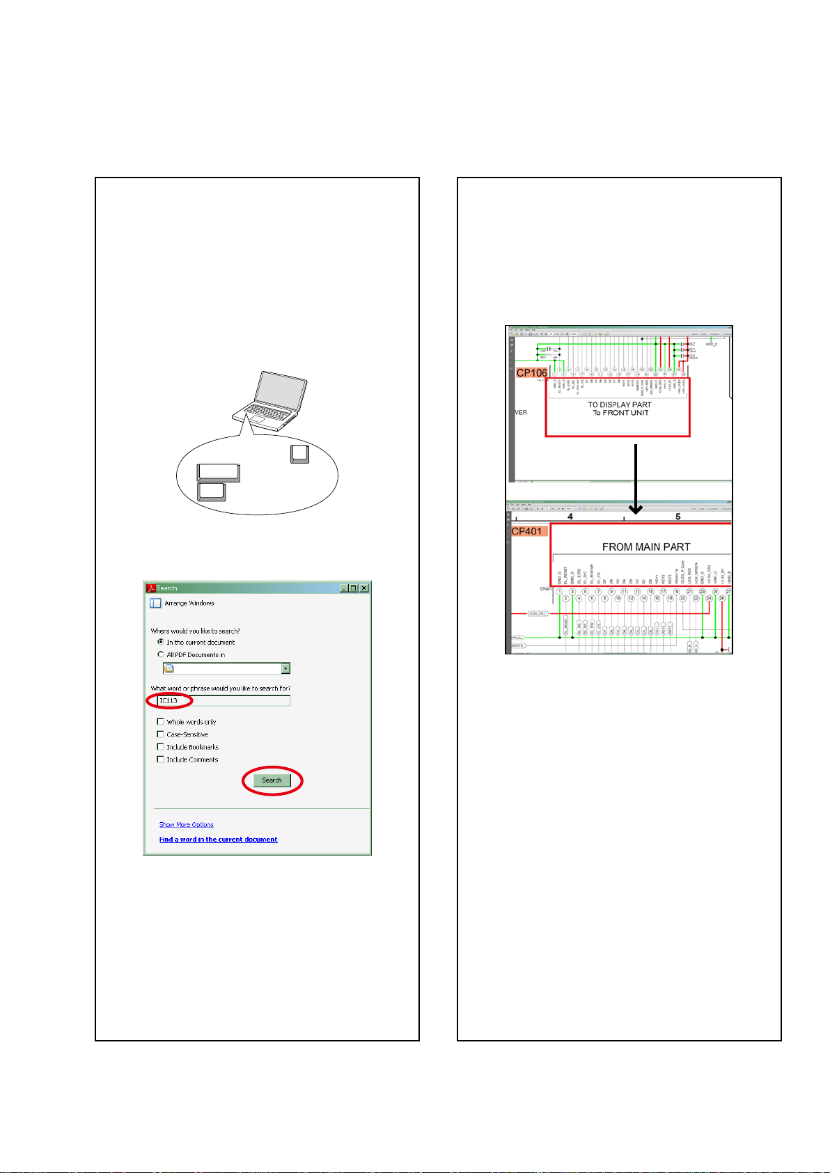
Search for a Ref. No. (phrase)
(Ctrl+Shift+F)
You can use the search function in Acrobat Reader to
search for a Ref. No. in schematic diagrams, printed
wiring circuit diagrams, block diagrams, and parts
lists.
1.Press
• The Search window appears.
2.EntertheRef.No.youwanttosearchforinthe
Search window, and then click the
•A list of search results appears.
Ctrl+Shift+F
Shift
Ctrl
onthekeyboard.
F
Search
button.
Jump to the target of a schematic
diagram connector
Click the Ref. No. of the target connector in the red
box around a schematic diagram connector.
•The screen jumps to the target connector.
CP401
v
CP106
3.Click an item on the list.
• The screen jumps to the page for that item, and the
searchphraseisdisplayed.
•Pagemagnicationstaysthesameasbeforethe
jump.
3
Using Adobe Reader (Windows version)
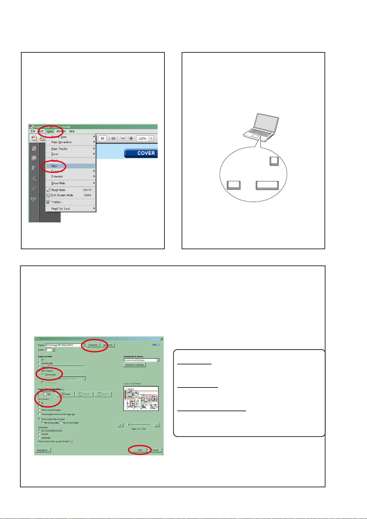
Add notes to this data (Sign)
TheSignfunctionletsyouaddnotestothedatain
this manual.
Savetheleonceyouhavenishedaddingnotes.
[Example using Adobe Reader X]
"View"
On the
• The Sign pane appears.
[Example using Adobe Reader 9]
On the
menu, click
"Document"
"Sign"
menu, click
.
"Sign"
.
Magnify schematic / printed circuit
board diagrams - 1
(Ctrl+Space, mouse operation)
Ctrl+Space
Press
mousetoselecttheareayouwanttoview.
• Theselectedareaismagnied.
• Whenyouwanttomovetheareashown,hold
Space
down
• Whenyouwanttoshowafullpageview,press
Ctrl+0
onthekeyboard.
onthekeyboardanddragthe
0
Ctrl Space
and drag the mouse.
Print a magnied part of the manual
ThePropertiesdialogboxandfunctionswillvarydependingonyourprinter.
1. Dragthemousetomagnifythepartyouwanttoprint.
2. On the
3. CongurethefollowingsettingsinthePrintdialogbox.
"File"
menu, click
"Print"
.
• Properties
Click this button and check that the printer is set to a
suitable paper size.
• Page to print
Select the following checkbox.
More Options
"
• Page Sizing & Handling
Select the following checkbox.
Size
"
Size Options
" / "
Current View
" : "
" : "
Fit
"
"
4. Click the
Print
button to start printing.
4
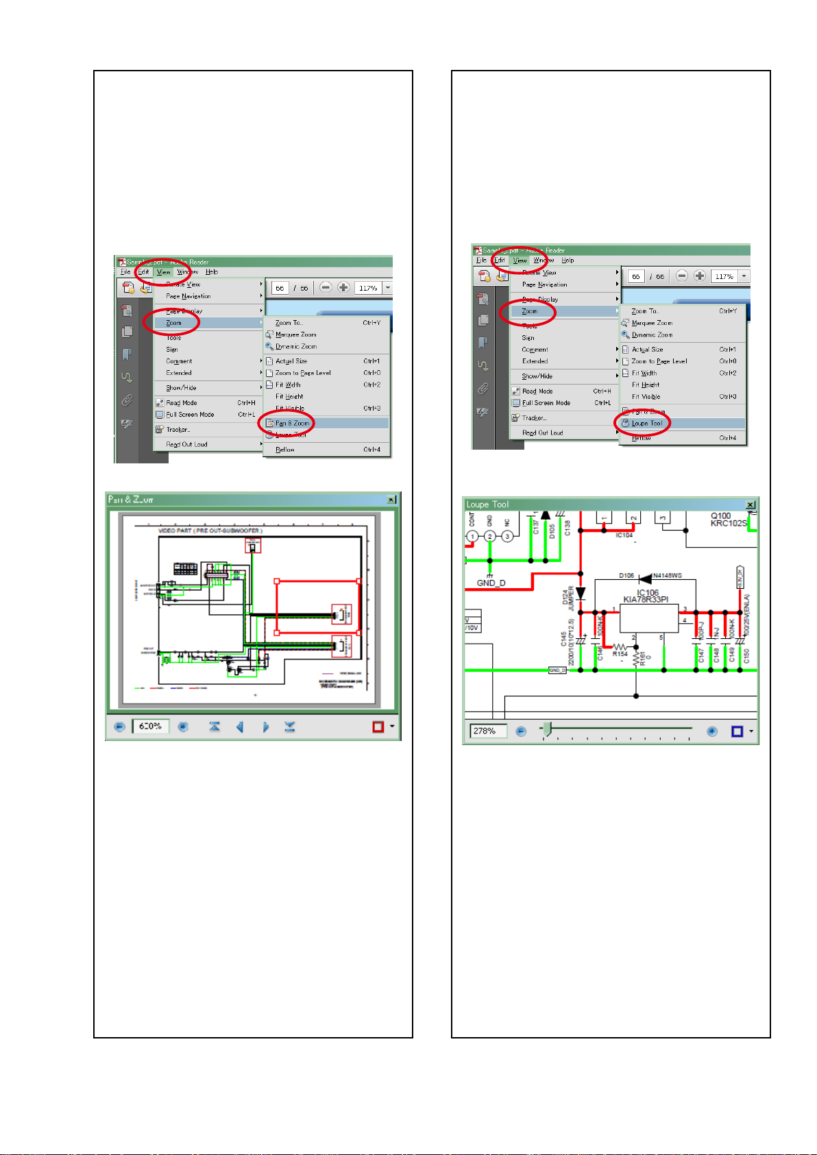
Magnify schematic / printed circuit
board diagrams - 2
(Pan & Zoom function)
ThePan&Zoomfunctionletsyouseewhichpartof
amagnieddiagramisbeingshowninaseparate
window.
[Example using Adobe Reader X]
"View"
On the
"Pan & Zoom"
menu, point to
.
"Zoom"
, and then click
Magnify schematic / printed circuit
board diagrams - 3
(Loupe Tool function)
TheLoupeToolfunctionletsyoumagnifyaspecic
part of a diagram in a separate window.
[Example using Adobe Reader X]
"View"
On the
"Loupe Tool"
menu, point to
.
"Zoom"
, and then click
• The Pan & Zoom window appears on the screen.
[Example using Adobe Reader 9]
"Tools"
On the
then click
menu, point to
"Pan & Zoom Window"
"Select & Zoom"
.
, and
• The Loupe Tool window appears on the screen.
[Example using Adobe Reader 9]
"Tools"
On the
then click
menu, point to
"Loupe Tool Window"
"Select & Zoom"
.
, and
5

SAFETY PRECAUTIONS
The following items should be checked for continued protection of the customer and the service technician.
leakage current check
Beforereturningthesettothecustomer,besuretocarryouteither(1)aleakagecurrentcheckor(2)alinetochassis
resistance check. If the leakage current exceeds 0.5 milliamps, or if the resistance from chassis to either side of the
power cord is less than 460 kohms, the set is defective.
Be sure to test for leakage current with the AC plug in both polarities, in addition, when the set's power is in each state
(on,offandstandbymode),ifapplicable.
CAUTION
Please heed the following cautions and instructions during servicing and
inspection.
◎Heed the cautions!
Cautions which are delicate in particular for servicing
are labeled on the cabinets, the parts and the chassis,
etc. Be sure to heed these cautions and the cautions
described in the handling instructions.
◎Cautions concerning electric shock!
(1) AnACvoltageisimpressedonthisset,soifyou
touch internal metal parts when the set is energized,
youmaygetanelectricshock.Avoidgettingan
electricshock,byusinganisolatingtransformer
and wearing gloves when servicing while the set is
energized,orbyunpluggingthepowercordwhen
replacing parts, for example.
(2) Therearehighvoltagepartsinside.Handlewith
extra care when the set is energized.
◎ Caution concerning disassembly and
assembly!
Through great care is taken when parts were
manufacturedfromsheetmetal,theremaybeburrson
theedgesofparts.Theburrscouldcauseinjuryifngers
are moved across them in some rare cases. Wear gloves
toprotectyourhands.
◎Use only designated parts!
Theset'spartshavespecicsafetyproperties(re
resistance,voltageresistance,etc.).Besuretouseparts
which have the same properties for replacement. The
burrs have the same properties. In particular, for the
importantsafetypartsthatareindicatedbythez mark
on schematic diagrams and parts lists, be sure to use
the designated parts.
◎ Be sure to mount parts and arrange the wires
as they were originally placed!
Forsafetyseasons,somepartsusetapes,tubesorother
insulatingmaterials,andsomepartsaremountedaway
from the surface of printed circuit boards. Care is also
takenwiththepositionsofthewiresbyarrangingthem
andusingclampstokeepthemawayfromheatingand
highvoltageparts,sobesuretoseteverythingbackas
itwasoriginallyplaced.
◎Make a safety check after servicing!
Check that all screws, parts and wires removed or
disconnected when servicing have been put back in their
original positions, check that no serviced parts have
deteriorate the area around. Then make an insulation
check on the external metal connectors and between
the blades of the power plug, and otherwise check that
safetyisensured.
(Insulationcheckprocedure)
Unplug the power cord from the power outlet, disconnect
the antenna, plugs, etc., and on the power. Using a 500V
insulation resistance tester, check that the insulation
resistancevaluebetweentheinplugandtheexternally
exposedmetalparts(antennaterminal,headphones
terminal,inputterminal,etc.)is1MΩorgreater.Ifitis
less, the set must be inspected and repaired.
CAUTION
Concerning important
safety parts
Manyoftheelectricandthestructuralpartsusedinthe
sethavespecialsafetyproperties.Inmostcasesthese
propertiesaredifculttodistinguishbysight,andtheuse
ofreplacementpartswithhigherratings(ratedpower
andwithstandvoltage)doesnotnecessarilyguarantee
thatsafetyperformancewillbepreserved.Partswith
safetypropertiesareindicatedasshownbelowonthe
wiring diagrams and the parts list in this service manual.
Be sure to replace them with the parts which have the
designated part number.
(1) Schematicdiagrams .......Indicatedbythez mark.
(2) Partslists .......Indicatedbythez mark.
The use of parts other than the
designated parts could cause electric
shocks,resorotherdangerous
situations.
6
NOTE FOR SCHEMATIC DIAGRAM
WARNING:
Partsindicatedbythezmarkhavecriticalcharacteristics.UseONLYreplacementpartsrecommendedbythemanufacturer.
CAUTION:
Beforereturningthesettothecustomer,besuretocarryouteither(1)aleakagecurrentcheckor(2)alinetochassisresistancecheck.
If the leakage current exceeds 0.5 milliamps, or if the resistance from chassis to either side of the power cord is less than 460 kohms, the
set is defective.
WARNING:
DONOTreturnthesettothecustomerunlesstheproblemisidentiedandremedied.
NOTICE:
ALLRESISTANCEVALUESINOHM.k=1,000OHM/M=1,000,000OHM
ALLCAPACITANCEVALUESAREEXPRESSEDINMICROFARAD,UNLESSOTHERWISEINDICATED.PINDICATESMICRO-MICRO
FARAD.EACHVOLTAGEANDCURRENTAREMEASUREDATNOSIGNALINPUTCONDITION.CIRCUITANDPARTSARESUBJECT
TOCHANGEWITHOUTPRIORNOTICE.
NOTE FOR PARTS LIST
1.Partsindicatedby
2.Whenorderingapart,makeacleardistinctionbetween"1"and"I"(i)toavoidmis-supplying.
3.Apartorderedwithoutspecifyingitspartnumbercannotbesupplied.
4.Partindicatedby"★" mark is not illustrated in the exploded view.
WARNING:
Partsindicatedbythezmarkhavecriticalcharacteristics.UseONLYreplacementpartsrecommendedbythemanufacturer.
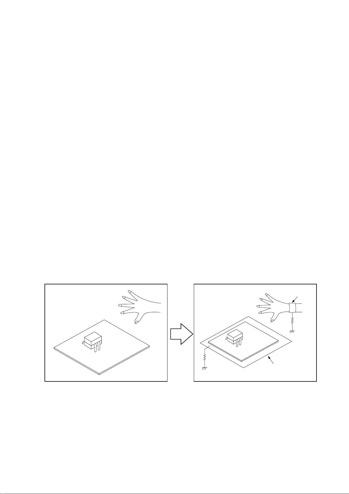
INSTRUCTIONS FOR HANDLING SEMI-CONDUCTORS AND OPTICAL UNIT
Electrostaticbreakdownofthesemi-conductorsoropticalpickupmayoccurduetoapotentialdifferencecausedby
electrostatic charge during unpacking or repair work.
"nsp"
on this table cannot be supplied.
1. GroundforHumanBody
Besuretowearagroundingband(1MΩ)thatisproperlygroundedtoremoveanystaticelectricitythatmaybe
chargedonthebody.
2. GroundforWorkbench
Besuretoplaceaconductivesheetorcopperplatewithpropergrounding(1MΩ)ontheworkbenchorothersurface,
wherethesemi-conductorsaretobeplaced.Becausethestaticelectricitychargeonclothingwillnotescapethrough
thebodygroundingband,becarefultoavoidcontactingsemi-conductorswithyourclothing
<Incorrect>
<Correct>
CBA
CBA
1MΩ
Grounding Band
1MΩ
Conductive Sheet or
Copper Plate
7

Personal notes:
8

TECHNICAL SPECIFICATIONS
nAudio section
• Power amplier
Rated output :
Front :
105W+105W(8Ω, 20Hz - 20kHz with 0.08% T.H.D.)
135W+135W(6Ω, 1kHz with 0.7% T.H.D.)
Center :
105W(8Ω, 20Hz - 20kHz with 0.08% T.H.D.)
135W(6Ω, 1 kHz with 0.7 % T.H.D.)
Surround :
105W+105W(8Ω, 20 Hz - 20 kHz with 0.08% T.H.D.)
135W+135W(6Ω, 1 kHz with 0.7 % T.H.D.)
Surround back :
105W+105W(8Ω, 20 Hz - 20 kHz with 0.08% T.H.D.)
135W+135W(6Ω, 1 kHz with 0.7 % T.H.D.)
Output connectors : 4 - 16 Ω
• Analog section
Input sensitivity/Input impedance : 200 mV / 47 kΩ
Frequency response : 10 Hz - 100 kHz — +1, -3 dB (Direct mode)
S/N ratio : 100 dB (IHF-A, Direct mode)
Rated output : 1.2V
• Digital section
D/A output : Rated output — 2 V (at 0 dB playback)
Digital input : Format — Digital audio interface
nVideo section
• Color component video connector
Input/output level and impedance : Y signal — 1 Vp-p, 75 Ω
Frequency response : 5 Hz - 60 MHz — 0, –3 dB
nTuner section
(Note : μV at 75 Ω, 0 dBf = 1 x 10
Reception frequency range : FM 87.5 MHz - 107.9 MHz (for E3)
Effective sensitivity : FM 1.2 μV (12.8 dBf) (for E3)
50 dB sensitivity : MONO ― 2.8 μV (20.2 dBf)
S/N ratio (IHF-A) : MONO ― 70 dB (for E3)
Total harmonic distortion — 0.008 % (1 kHz, at 0 dB)
S/N ratio — 102 dB
Dynamic range — 100 dB
PB / CB signal — 0.7 Vp-p, 75 Ω
PR / CR signal — 0.7 Vp-p, 75 Ω
–15
FM 87.5 MHz - 108.0 MHz (for E2, E1C)
AM 520 kHz - 1710 kHz (for E3)
AM 522 kHz - 1611 kHz (for E2, E1C)
FM 1.2 μV (12.8 dBf) (for E2, E1C)
AM 18 μV (for E3)
AM 18 μV (for E2, E1C)
MONO ― 78 dB (for E2, E1C)
STEREO ― 67 dB (for E3)
STEREO ― 67 dB (for E2, E1C)
W)
Distortion : MONO ― 0.7 % (for E3)
MONO ― 0.7 % (1 kHz) (for E2, E1C)
SRETEO ― 1.0 % (for E3)
SRETEO ― 1.0 % (1 kHz) (for E2, E1C)
nWireless LAN section
Network type (wireless LAN standard) : Conforming to IEEE 802.11b
Security : WEP 64 bit, WEP 128 bit
Radio frequency : 2.4 GHz
No. of channels : 1 - 11 ch (for E3)
z1 The Wi-Fi® CERTIFIED Logo and the Wi-Fi CERTIFIED On-Product Logo
are registered trademarks of the Wi-Fi Alliance.
WPA/WPA2-PSK (AES)
WPA/WPA2-PSK (TKIP)
1 - 13 ch (for E2, E1C)
Conforming to IEEE 802.11g
Conforming to IEEE 802.11n
(Wi-Fi® compliant)z1
nBluetooth section
Communications system : Bluetooth Version 2.1 + EDR
Transmission power : Maximum 2.5 mW (Class 2)
Maximum communication range : Approx. 32.8 ft/10 m in line of sight
Frequency band : 2.4 GHz band
Modulation scheme : FHSS (Frequency-Hopping Spread Spectrum)
Supported proles : A2DP (Advanced Audio Distribution Prole)1.2
Corresponding codec : SBC, AAC
Transmission range (A2DP) : 20 Hz - 20,000 Hz
z2 The actual communication range varies depending on the inuence of
such factors as obstructions between devices, electromagnetic waves
from microwave ovens, static electricity, cordless phones, reception
sensitivity, antenna performance, operating system, application
software etc.
(Enhanced Data Rate)
AVRCP (Audio Video Remote Control Prole)1.4
nGeneral
Power supply : (for E3) : AC 120 V, 60 Hz
Power consumption : 600 W
Power consumption in standby mode : 0.1 W
Power consumption in CEC standby mode : 0.5 W
Power consumption in network standby mode : 2.7 W
For purposes of improvement, specications and design are subject to
change without notice.
(for E2) : AC 230 V, 50 Hz / 60 Hz
(for E1C) : AC 220 V, 50 Hz
9
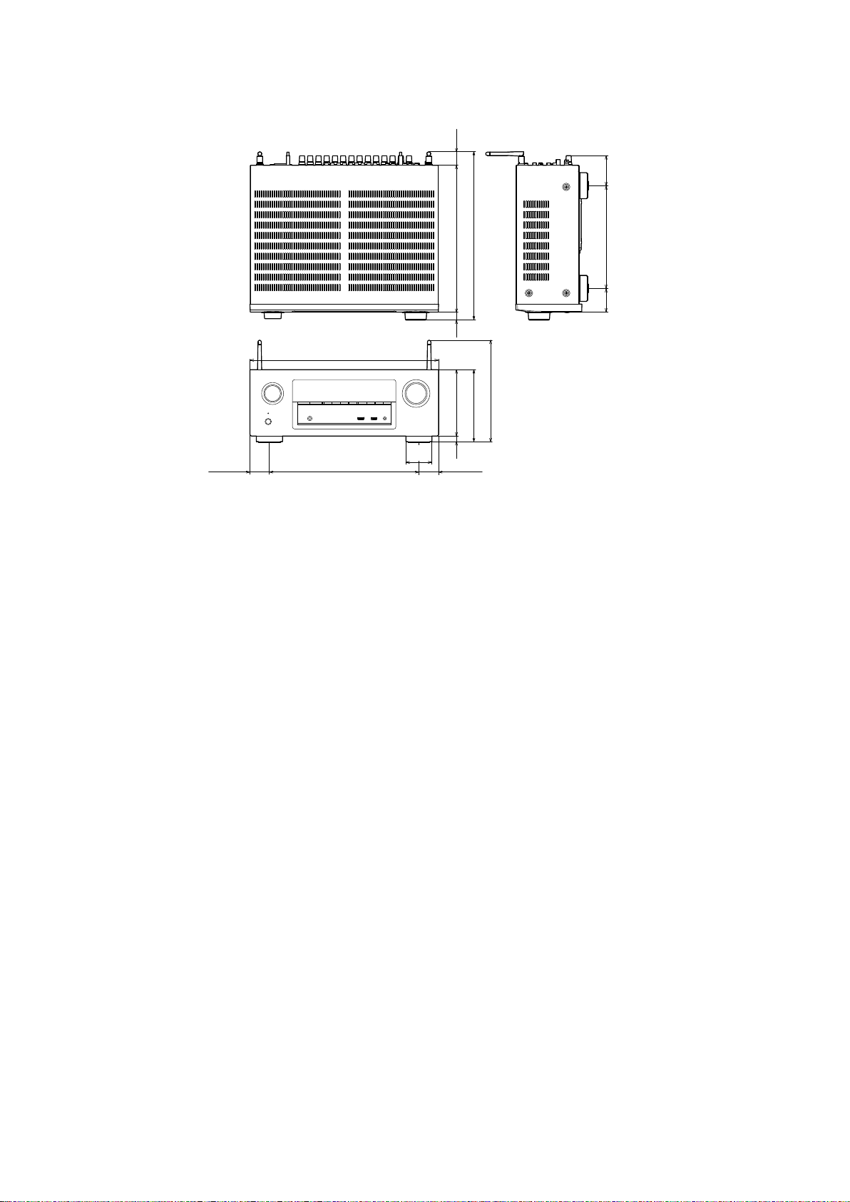
DIMENSION
Unit : in. (mm)
Weight : 24 lbs 15 oz (11.3 kg)
1 1/4
(31)
1 7/8
(47)
13 3/8 (339)
15 3/8 (388)
3/4
(19)
17 1/8 (434)
6 5/8 (167)
9 3/8 (237)
2 3/8
5/8
(15) 6 (152)
..
13 1/2 (340)
(60)
)74( 8/7 1)74( 8/7 1
9 3/8 (237)
(55)
2 1/4
10
CAUTION IN SERVICING
SOURCE
Initializing This Unit
Make sure to initialize this unit after replacing the microcomputer or any peripheral equipment, or the digital PCB.
1. Press the power button to turn off the power.
2. While holding down buttons "
ZONE2 SOURCE
the power.
3. Release the buttons after conrming that the display ashes at 1-second intervals.
* The unit is initialized.
" and "
DIMMER
" simultaneously, press the power button to turn on
NOTE:
• If the unit fails to enter the service mode in step 3, repeat the procedure from step 1.
• Initializing the device restores the customized settings to the factory settings. Write down your settings in advance and
recongure the settings after initialization.
SOURCE SELECT
ZONE2
TUNER
PRESET CH
PHONES
ON/OFF
ZONE2
SOURCE
DIMMER STATUS
DIMMERX ZONE2
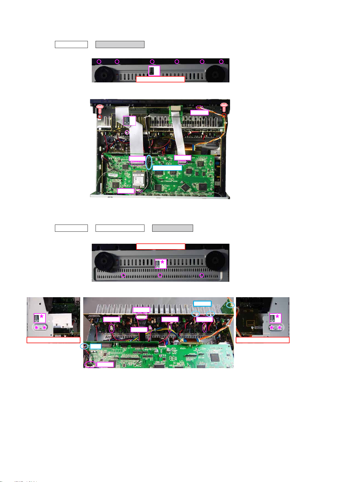
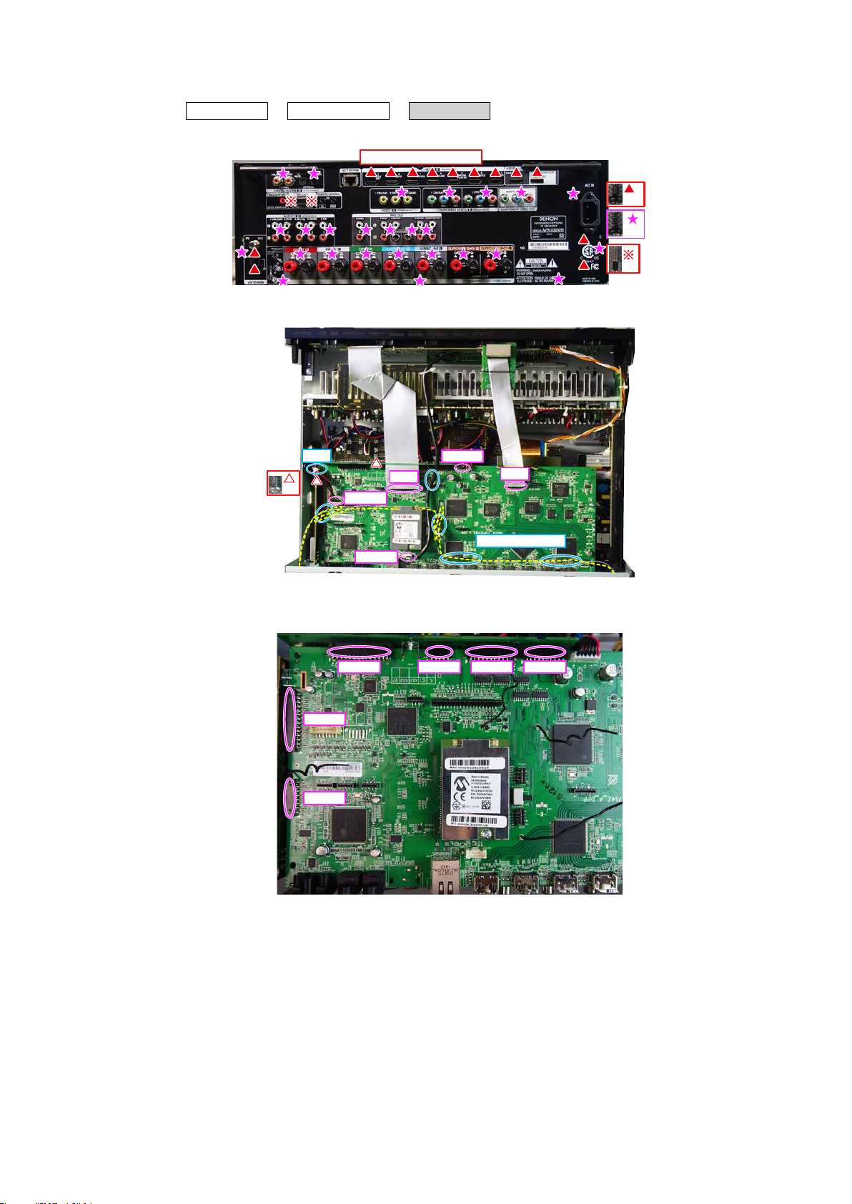
JIG FOR SERVICING
Use the following jigs (extension cable kit) when repairing the PCBs.
Order with your dealer for the jigs your dealer if necessary.
Blu-rayCBL/SAT
QUICK SELECT
MASTER VOLUME
MEDIA
ONLINE
32 41
PLAYER
SETUP MICAUX1 - HDMI
8U-110084S : EXTENSION UNIT KIT : 1Sets
8U-110136S : EXTENSION UNIT KIT : 1Sets
(See page 64)
11
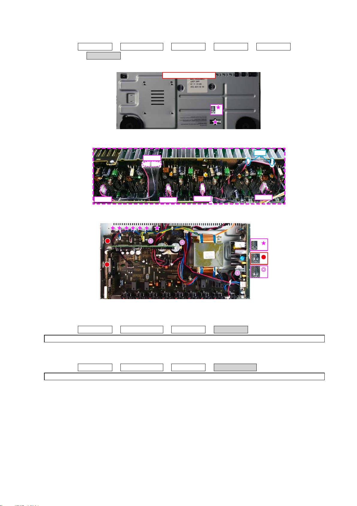
DISASSEMBLY
• Remove each part following the ow below.
• Reassemble the removed parts in the reverse order.
• Read "Precautions During Work" before reassembling the removed parts.
• If wire bundles are removed or moved during adjustment or part replacement, reshape the wires after completing
the work. Failure to shape the wires correctly may cause problems such as noise.
TOP COVER
FRONT PANEL ASSY
See "DISASSEMBLY"
1. FRONT PANEL ASSY
and "EXPLODED VIEW"
FRONT PCB
Ref. No. of EXPLODED VIEW : C1
FRONT HDMI FFC CABLE PCB
Ref. No. of EXPLODED VIEW : C4
FRT HDMI PCB
Ref. No. of EXPLODED VIEW : C5
FRONT FFC PCB
Ref. No. of EXPLODED VIEW : C10
RADIATOR ASSY
See "DISASSEMBLY"
2. RADIATOR ASSY
and "EXPLODED VIEW"
GUIDE L PCB
Ref. No. of EXPLODED VIEW : C7
AMP PCB
Ref. No. of EXPLODED VIEW : C8
HEATSINK
Ref. No. of EXPLODED VIEW : M8
DIGITAL PCB ASSY
See "DISASSEMBLY"
3. DIGITAL PCB ASSY
and "EXPLODED VIEW"
DIGITAL PCB
Ref. No. of EXPLODED VIEW : C16
CY920 MODULE ASSY
Ref. No. of EXPLODED VIEW : C17
VIDEO PCB ASSY
See "DISASSEMBLY"
4. VIDEO PCB ASSY
and "EXPLODED VIEW"
PCB
VIDEO
Ref. No. of EXPLODED VIEW : C14
INPUT PCB ASSY
See "DISASSEMBLY"
5. INPUT PCB ASSY
and "EXPLODED VIEW"
INPUT PCB
Ref. No. of EXPLODED VIEW : C11
SPK PCB ASSY
See "DISASSEMBLY"
6. SPK PCB ASSY
and "EXPLODED VIEW"
SPK PCB
Ref. No. of EXPLODED VIEW : C31
FUSE PCB
Ref. No. of EXPLODED VIEW : C29
FRT CNT PCB
Ref. No. of EXPLODED VIEW : C28
SIDE CONT PCB
Ref. No. of EXPLODED VIEW : C30
SMPS PCB
See "DISASSEMBLY"
7. SMPS PCB
and "EXPLODED VIEW"
SMPS PCB
Ref. No. of EXPLODED VIEW : C20
MAIN TRANS
See "DISASSEMBLY"
8. MAIN TRANS
and "EXPLODED VIEW"
MAIN TRANS
Ref. No. of EXPLODED VIEW : C13
12
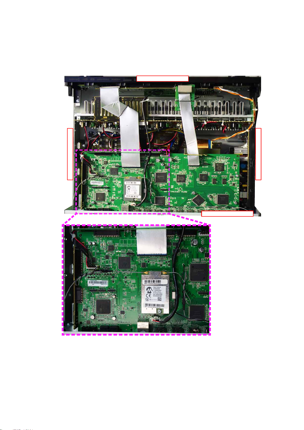
Explanatory Photos for DISASSEMBLY
• For the shooting direction of each photos used in this manual, see the photo below.
• A, B, C and D in the photo below indicate the shooting directions of photos.
• The photographs with no shooting direction indicated were taken from the top of the unit.
• Photos of AVR-X3200W E3 are used in this manual.
The viewpoint of each photograph
(Shooting direction : X) [View from the top]
↓Shooting direction: B↓
↓Shooting direction: D↓
↑Shooting direction: C↑
↑Shooting direction: A↑
13
1. FRONT PANEL ASSY
Proceeding : TOP COVER
(1) Remove the screws.
(2) Remove the screws. Remove the STYLE PIN and connector wire. Remove the FFC.
→
FRONT PANEL ASSY
CN321
x6
View from the bottom
x1
FFC
STYLE PIN
CN602
FFC
2. RADIATOR ASSY
Proceeding : TOP COVER
(1) Remove the screws.
(2) Cut the wire clamp, then remove the STYLE PIN and connector wire. Remove the screws.
x2 x2
↑Shooting direction: D↑
→
FRONT PANEL ASSY→RADIATOR ASSY
Shooting direction: A
x3
CN461
CN701 CN702 CN704
CN703
CUT
CN704
CUTx3
↑Shooting direction: C↑
14
3. DIGITAL PCB
Proceeding : TOP COVER
(1) Remove the screws.
(2) Cut the wire clamp, then remove the STYLE PIN, FFC and connector wire.
→
BACK CHASSIS
CUT
x2
CN704
→
DIGITAL PCB
Shooting direction: A
CN903
FFC
FFC
x13
x26
x2
(3) Remove the connector.
STYLE PIN x5
CN321
BN24A BN26A BN25A BN21A
BN23A
BN27A
15
4. VIDEO PCB
Proceeding : TOP COVER
→
BACK CHASSIS
→
(1) Cut the wire clamp, then remove the connector.
BN28B
BN27B
5. INPUT PCB
Proceeding : TOP COVER
(1) Remove the connector.
→
BACK CHASSIS
BN64C
BN23C
→
BN26CBN24C
DIGITAL PCB
BN21B
DIGITAL PCB
From AMP PCB
→
→
CN706
VIDEO PCB
CUT x4
VIDEO PCB
→
INPUT PCB
16
6. SPK PCB
Proceeding : TOP COVER
→
SPK PCB
→
BACK CHASSIS
→
DIGITAL PCB
(1) Remove the screws.
View from the bottom
(2) Cut the wire clamp, then remove the connector wire.
CN461
CN701
CN703
(3) Remove the screws.
CN702
→
x1
VIDEO PCB
→
CUT
CN704
INPUT PCB
7. SMPS PCB
Proceeding : TOP COVER
8. TRANS POWER
Proceeding : TOP COVER
See "EXPLODED VIEW" for instructions on removing the transformer (TRANS).
→
BACK CHASSIS
→
DIGITAL PCB
→
SMPS PCB
See "EXPLODED VIEW" for instructions on removing the SMPS PCB.
→
BACK CHASSIS
→
DIGITAL PCB
→
TRANS POWER
x7
x2
x3
17
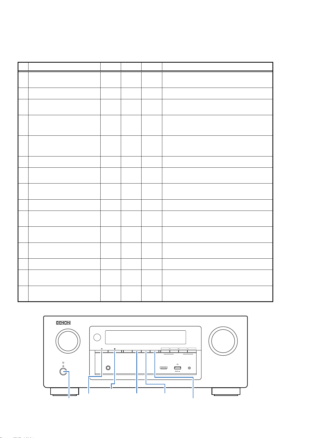
SPECIAL MODE
STATUS
X
SOURCE
PRESET CH -
Special mode setting button
No. 1 - 6, 9 : While holding down buttons "A", "B" and "C" simultaneously, press the power button to turn on the power.
b
No. 7, 8 : While the power is on, hold down buttons "A" and "B" for at least 3 seconds.
b
No. 10 : While holding down buttons "A" and "B" simultaneously, insert the AC plug into the wall outlet to turn on the power.
b
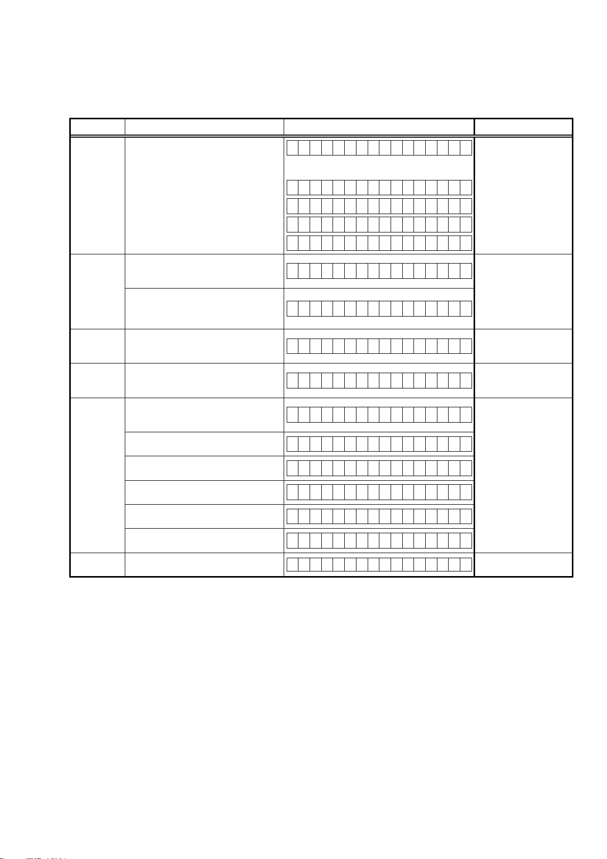
No. Mode Button A Button B Button C Descriptions
Version Display
1
(u-COM / DSP Error Display)
Selecting the Mode for Service-related
2
DIMMER STATUS -
ZONE2
SOURCE
DIMMER STATUS
TUNER
Protection history display mode
2-1
Check the Video/Audio path Mode ↑ - -
2-2
Remote ID Setup Mode ↑ - -
2-3
TUNER STEP Mode
2-4
(E3 and E2 model only)
Operation Info Mode ↑ - -
2-5
User Initialization Mode
3
PRESET CH +- -
↑ - -
TUNER
PRESET CH
TUNER
PRESET CH +-
-
Factory Initialization Mode
4
PANEL / REMOTE LOCK Selection Mode
5
Protection Pass Mode
6
CY920 Reboot Mode
7
ZONE2
SOURCE
TUNER
PRESET CH
+
TUNER
PRESET CH
-
TUNER
PRESET CH
DIMMER -
ZONE2
SOURCE
ZONE2
SOURCE
TUNER
PRESET CH +- The CY920 is restarted after CY920 hang up.
-
CY920 Initialization Mode
8
USB Update Mode
9
ZONE2
SOURCE
TUNER
PRESET CH
DIMMER -
STATUS
-
TUNER
Forced USB All Device Write Mode
10
PRESET CH -STATUS -
STATUS
s
Displays the version of rmware such as the main rmware or DSP.
Errors that have occurred are displayed.
(See page 19 )
This is a display for turning on each service-related mode.
Service-related modes: No. 2-1 - No. 2-5
Displays the protection occurrence history.
(See page 57)
This is a special mode for service conrmation used during repair
work to simplify the conrmation work for the Audio channel /
video channel.
(See page 28)
If there are multiple DENON AV receivers in the same area, this
mode prevents other AV receivers from being operated concurrently with this device.
(See page 61)
Enables reception STEP of the ANALOG TUNER to be changed.
(See page 60)
Displays the accumulated operating time of the unit, the number
of times the power was switched on, and the number of occurrences of each protection. (See page 59)
Initializes backup data.
(Settings for the Installer Setup are not initialized.)
Initializes backup data.
(The settings for the Installer Setup is also initialized.)
Start this unit in the PANEL/REMOTE LOCK selection mode so that
-
PANEL LOCK and Remote Lock can be switched between ON and
OFF. (See page 23)
Enables the power to be turned on when protection detection is
disabled. (See page 62)
Enter this mode only after replacing Flash for CX870 / CY920 and
rewriting the rmware.
- Switches this unit to USB Update mode.
Mode used when this unit cannot be recovered.
Forcibly switches this unit to USB update mode.
(See page 70)
SOURCE SELECT
TUNER
TUNER
PRESET CH
PHONES
TUNER
PRESET CH +
ZONE2
ON/OFF
ZONE2
SOURCE
ZONE2
DIMMER STATUS
18
DIMMER
Blu-rayCBL/SAT
QUICK SELECT
MASTER VOLUME
MEDIA
ONLINE
32 41
PLAYER
SETUP MICAUX1 - HDMI
1. Version Display Mode
1.1. Actions
Version information is displayed when the device is started in this mode.
1.2. Starting up
While holding down buttons "DIMMER" and "STATUS" simultaneously, press the power button to turn on the power.
then press the "STATUS" button to display the information in section 1.3 on the display.
The version list is also displayed on GUI while the version is displayed on the display.
b
1.3. Display Order
Error information(See "1.4. Error display") → q Model destination information → w Serial Number
→ e Firmware Package Version → r Main µ-com → t Main 1st Boot Loader → y DSP ROM
→ u Audio PLD → i Video PLD → o GUI SFLASH → Q0 Ethernet 1st Boot Loader, Hardware ID
→ Q1 Ethernet 2nd Boot Loader, Rhapsody Flag → Q2 Ethernet IMAGE → Q3 Ethernet MAC ADDRESS information
→ Q4 BT MAC Address information
Model destination information :
q
FLD
A V R - X 3 2 0 0 W E 3 *
FLD
A V R - X 3 2 0 0 W E 2 *
FLD
A V R - X 3 2 0 0 W E 1 C *
Serial Number:
w
FLD
S / N . * * * * * * * * * *
Firmware Package Version:
e
FLD
P a c k a g e : * * * *
Main µ-com Version information :
r
FLD
* : Main version, #: Sub version
Main 1st Boot Loader :
t
FLD
DSP ROM :
y
FLD
Audio PLD :
u
FLD
Video PLD
i
FLD
M a i n : * * * * # # # # *
M a i n F B L : * * . * *
D S P : * * . * *
A u d i o P L D : * * . * *
V i d e o P L D : * * . * *
GUI SFLASH :
o
FLD
@ : Model code, $ : Brand code, \ : Region code, * : version
G U I : @ @ $ \ * * * *
19
Ethernet 1st Boot Loader, Hardware ID :
Q0
FLD
E t h e r n e t F B L
Press "
FLD
* * * * * * - b d
Ethernet 2nd Boot Loader, Rhapsody Flag :
Q1
FLD
Press "
FLD
Ethernet IMAGE :
Q2
FLD
Press "
FLD
Ethernet MAC ADDRESS information:
Q3
FLD
E t h e r n e t S B L
B * * * * * * * * * * * * - 0 A
E t h e r n e t I M G
I * * * * * * * * * * * *
* N E T M A C A d d r e s s
STATUS
STATUS
STATUS
" button.
" button.
" button.
Press "
FLD
BT MAC ADDRESS information:
Q4
FLD
Press "
FLD
* * * * * * - * * * * * *
* B T M A C A d d r e s s
* * * * * * - * * * * * *
STATUS
STATUS
" button.
" button.
20
1.4. Error display
See the table below for descriptions of the displayed errors and countermeasures for these.
If multiple errors occur, only one item is displayed.
Item is displayed. The priority order is w, e, r, t, y, q.
Condition States Display TROUBLE SHOOTING
q
Firm Check
NG
w
IP SCALER NG
e
GUI Serial
Flash NG
r
DIR NG
t
DSP NG
y
EEPROM NG
The model name, brand name and region
information written in the rmware are
compared to the region settings in the
PCB. This error is displayed if the information does not match.
" ▲ " or " ▼ " is displayed as the rst character if the rmware is not correct (see the
illustrations on the right).
An error occurs in Loopback Test of the
DDR memory which is performed during
the initial setting of i/p Scaler (ADV8003).
During the initial setting of i/p Scaler
(ADV8003), there is not the reply of the
Loopback Test result of the DDR memory.
If the Main CPU version is not supported
by the GUI Serial Flash (ADV8003),
This error is displayed if there is no response from the DIR.
The DSP FLAG0 port does not enter "Hi"
status while booting a DSP code even
after resetting DSP.
The DSP FLAG0 port does not enter "Hi"
status before issuing a DSP command.
Setting WRITE to "Lo" does not set ACK to
"Hi" during DSP data reading.
Setting REQ to "Lo" does not set ACK to
"Lo" during DSP data reading.
Setting WRITE to "Hi" does not set ACK to
"Hi" during DSP data writing.
Setting REQ to "Lo" does not set ACK to
"Lo" during DSP data writing.
An error occurred in a checksum of the
EEPROM(
***
is a block address number).
F I R M E R R O R
–
M a i n : * * * * * * * *
–
D S P : * * . * *
–
A u d i o P L D : * * . * *
•
G U I : * * * * * * * *
I P S C A L E R E R R 0 1
I P S C A L E R E R R 0 2
G U I V E R . E R R O R
D I R E R R O R 0 1
D S P E R R O R 0 1
D S P E R R O R 0 2
D S P E R R O R 0 3
D S P E R R O R 0 4
D S P E R R O R 0 5
D S P E R R O R 0 6
E 2 P R O M E R R * * *
• Check the resistor for
setting the region
(R1589/R1590 DIGITAL
PCB).
• Write the rmware for
the correct region.
• Check the circuits
around the IP SCALER
(IC104, DIGITAL PCB)
and DDR2 (IC402/IC403).
• If there appear to be
no problems, IC104 or
IC402/IC403 is faulty.
• Check the rmware
version.
• Check the DIR (IC202,
DIGITAL PCB) and surrounding circuits.
• Check the DSP (IC251,
DIGITAL PCB) and surrounding circuits.
21
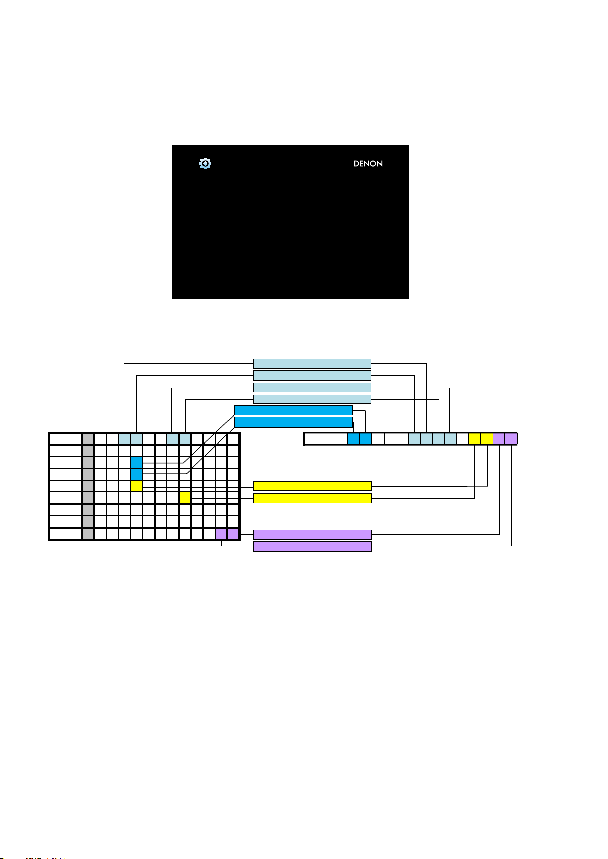
1.5. Version Display in the Setup Menu
Follow the steps below to display the rmware information.
(1) Press the "
SETUP
" button on the remote control.
(2) Select "General - Information - Firmware".
The version information is displayed as a 12-digit number as shown in the screenshot below.
General/Firmware
Version
XXXX - XXXX - XXXX
GUI Image
This 12-digit number comprises a part of the version number of each device and module.
These version numbers correspond to the 14-digit number as shown below.
Main
M.FBL
X X 3 8
X X X X
X X 2 8
X X X X
The 2nd digit from the right for Main
The 1th digit from the right for Main
The 2nd digit from the right for Sub
The 1st digit from the right for Sub
The 1st digit from the right for DSP
The 1st digit from the right for A.PLD
Info display
1 2 0 0 - 8 3 8 2 - 6 7 7 3
DSP X X X 2
A.PLD
V.PLD
GUI X X X X X X X 6
X X X 1
X X X 7
The 1st digit from the right for V.PLD
The 1st digit from the right for GUI
E.FBL X X X X X X
E.SBL B X X X X X X X X X X X X
E.IMG I X X X X X X X X 0 0 3 7
The 1st digit from the right for IMG
The 2nd digit from the right for IMG
The rmware version numbers and this 12-digit version information are written in the Service Information.
b
22
2. PANEL / REMOTE LOCK Selection Mode
2.1. Actions
Switch the PANEL LOCK and REMOTE LOCK modes between on and off.
2.2. Starting up
While holding down buttons "
turn on the power.
Select the desired mode using the "
TUNER PRESET CH+
TUNER PRESET CH+
2.3. Displaying and Selecting Each Mode
The information shown on the display switches each time the "
Press the "
The setting with "*" is selected for each mode.
q
FLD
The buttons on the unit and the master volume knob does not function.
w
FLD
The buttons on the unit does not function.
STATUS
" button to set the currently displayed mode and restart the device.
F P / V O L L O C K * O N
F P L O C K O N
ZONE2 SOURCE
" and "
" button, then press the "
TUNER PRESET CH+
" simultaneously, press the power button to
STATUS
" button to conrm.
" button is pressed.
e
FLD
The PANEL LOCK mode is turned off.
r
FLD
The device cannot be operated by the remote control.
t
FLD
The REMOTE LOCK mode is turned off.
F P L O C K O F F
R C L O C K O n
R C L O C K * O F F
23
3. Selecting the Mode for Service-related Operations
3.1. Actions
Select diagnostic mode (service path check mode), protection history display mode, or 232C standby clear mode.
3.2. Starting up
While holding down buttons "
turn on the power.
Select the desired mode using the "
ZONE2 SOURCE
TUNER PRESET CH+
3.3. Displaying and Selecting Each Mode
The information shown on the display switches each time the "
Press the "
q
FLD
Service Path Check Mode:
The Video and Audio paths can be checked.
This function is convenient for conrming problem paths in the product and checking the paths
after repairing.
w
FLD
The protection history can be checked.
STATUS
" button to set the currently displayed mode and restart the device.
1 . S E R V I C E C H E C K
2 . P R O T E C T I O N
DIMMER
", "
STATUS
" and "
" button, then press the "
TUNER PRESET CH+
" simultaneously, press the power button to
STATUS
" button to conrm.
" button is pressed.
e
FLD
Switches from 232C standby mode to normal standby mode.
r
FLD
Operation Info for the unit can be checked.
t
FLD
Enables reception STEP of the ANALOG TUNER to be changed.
y
FLD
This function is for operating only the desired AV receiver.
3 . R S 2 3 2 C R E S E T
4 . O P I N F O
5 . T U N E R F R Q S E T
6 . R E M O T E I D
3.3. Canceling the selected mode
Press the power button to turn off the power.
24
3.4 PROTECTION DIAGRAM
TR_THERMAL
FL
TR_THERMAL
FR
TR_THERMAL
C
TR_THERMAL
SL
TR_THERMAL
SR
TR_THERMAL
ASO
DC
ASO
DC
ASO
DC
ASO
DC
ASO
DC
PAMP PCB
BN701 CN704
DC_DET2
DC_DET1
ASO_DET
THERMAL_DETA
THERMAL_DETB
THERMAL_DETE
THERMAL_DETF
DIGITAL PCB
DC_DET2
DC_DET1
ASO_DET
THERMAL_DETA
THERMAL_DETB
THERMAL_DETE
THERMAL_DETF
uCOM
PROTECTION LOGIC
DC ⇒ L_activeshutdown
ASO ⇒ L_activeshutdown
THER PROTF ⇒ L_activeshutdown
THER PROTB ⇒ L_activeshutdown
THER PROTA ⇒ L_activeshutdown
CURRENT (After 90sec )
Over 1.0V & Low B & THERMAL E = Low ⇒ shutdown
Over 2.0V ⇒ shutdown
DC/ASO PROT 125pin/AN105
THER_PROT_E 161pin/P91
THER_PROT_F 163pin/P90
THER_PROT_A 159pin/P93
CURRENT_DET 166pin/AN006
SBL
TR_THERMAL
SBR
HEATSINK_THERMAL
HEATSINK_THERMAL
ASO
DC
ASO
DC
SPEAKER PCB FRONT CNT PCB
CURRENT DETECT PART
CPU LEVEL CHG PART
BN25D 15pinCN25D 15pin
CURRENT DET
CN25A 9pin
CURRENT DET
BN25A 9pin
CURRENT DET CURRENT DET
25
3.5. DIAGNOSTICMODE(ServicePathCheckMode)
3.5.1.Actions
This function is convenient for conrming problem paths in the product and executing a path check after repair.
The Video and Audio paths can be checked.
The backup data is not rewritten.
3.5.2.Startingup
Hold down buttons "
ZONE2 SOURCE
Select the mode using the button "
Select "
The "
1. SERVICE CHECK
TUNED
", "
STERO
" and press the "
RDS
" and "
DIMMER
", "
TUNER PRESET CH+
STATUS
STATUS
" and "
", and press the button "
" button to start the diagnostic mode.
" segments are lit in this mode.
" at the same time and press the power button to turn on the power.
STATUS
" to commit the selection.
3.5.3.Cancelingdiagnosticmode
Press the power button to turn off the power.
3.5.4.Selectingitems
Press q button to switch between video items and audio items.
Press button w or e to select the previous or next item.
The unit Remote control unit
Actions
Button DIMMER QUICK SELECT 1 QUICK SELECT 2 SLEEP CURSOR LEFT CURSOR RIGHT
q w e q w e
Audio ⇔ Video PREVIOUS NEXT Audio ⇔ Video PREVIOUS NEXT
3.5.5.Videosystemconrmationitems
g. XX: See the block diagram of the g.XXth.
Paths conrmation item Display Settings Contents of conrmation Remarks
Analog Video
1
Video Convert
(Analog or HDMI ⇒ HDMI)
2
HDMI pass
(MAIN ZONE)
3
HDMI CEC
4
HDMI Audio
(Audio: AVR)
5
HDMI Audio
(Audio: TV)
6
g.01
g.02a
g.02b
g.03
g.04
g.05a
g.05b
g.05c
g.06a
g.06b
V 0 1 : V I D E O P A S S
V 0 2 : V . C O N V E R T
V 0 3 : H D M I P A S S
V 0 4 : H D M I C E C
V 0 5 : H . A U D I O - A V R
V 0 6 : H . A U D I O - T V
Input Source : CBL/SAT
Video Convert(IP Scaler) : OFF, All sources
MAIN ZONE : ON
ZONE2 : ON
Input Source : CBL/SAT
Video Convert(IP Scaler) : ON, All sources
IP Scaler : "Analog & HDMI", All sources
Resolution : "Auto", All sources
MAIN ZONE ON
ZONE2 OFF
Input Source : CBL/SAT
Source of Video Convert(IP Scaler) : OFF, All sources
MAIN ZONE ON
ZONE2 OFF
Input Source : CBL/SAT
HDMI Control : ON
MAIN ZONE ON
ZONE2 OFF
Input Source : CBL/SAT
HDMI Control : OFF
HDMI Audio:AVR ( if checking the audio output from AVR )
HDMI Audio:TV ( if checking the audio output from TV ) ・Check of HDMI input(PCM , DolbyDigital , DTS) ⇒ HDMI output (audio output from connected TV)
・Component input ⇒ Component output (E3 ONLY)
( ※ As the input source, you can switch from CBL/SAT to other ones.
・Check of CVBS input ⇒ IP Scaler ⇒ HDMI output.
・Check of Component input ⇒ IP Scaler ⇒ HDMI output.
・Check of HDMI input ⇒ IP Scaler ⇒ HDMI output.
・Check of ETHERNET input ⇒ IP Scaler ⇒ HDMI output.
(※ The input source can be switched to any source except CBL/SAT.)
・Check of HDMI input(MAIN Function)⇒ HDMI output(MAIN)
(※ The input source can be switched to any source except CBL/SAT.)
・ When the power supply of a TV is put in the standby mode, make sure that the power supply of this unit is also put
in the standby mode.
・The ARC path can also be checked (check this using the TV input source).
(※ The input source can be switched to any source except CBL/SAT.)
・Check of HDMI input(PCM , DolbyDigital , DTS) ⇒ Speaker output.
・Check of HDMI input(HD audio) ⇒ Speaker output.
(※ The input source can be switched to any source except CBL/SAT.)
(※ The input source can be switched to any source except CBL/SAT.)
7
8
GUI
HDMI
(ZONE2)
g.07
g.08
V 0 7 : G U I M E N U O N
V 0 8 : Z O N E 2 H D M I
Input Source : CBL/SAT
Video Convert(IP Scaler) : ON, All sources
IP Scaler : "Analog & HDMI", All sources
Resolution : "AUTO", All sources
Setup Menu ON
MAIN ZONE ON
ZONE2 OFF
Input Source : CBL/SAT
ZONE2 Source : Source
MAIN ZONE : ON
ZONE2 : ON
・Check of GUI display ⇒ HDMI output.
(※ The input source can be switched to any source except CBL/SAT.)
・HDMI input (ZONE2 Function) ⇒ HDMI output (ZONE2)
( ※ As the input source, you can switch from CBL/SAT to other ones.)
26
3.5.6.Audiosystemconrmationitems
g. XX: See the block diagram of the g.XXth.
Paths conrmation item Display Settings Contents of conrmation Remarks
Analog
1
Digital
(MAIN ZONE)
2
Digital (signal) Path
(ZONE2)
3
HDMI
4
A/D
(MAIN ZONE)
5
Amp Assign
(Amp Assign : ZONE2)
6
Amp Assign
( Amp Assign :
7
5.1ch (Bi-Amp)
Front Height
8
Front Wide
9
g.09
g.10a
g.10b
g.11a
g.11b
g.12a
g.12b
g.12c
g.13a
g.13b
g.14
g.15a
g.15b
g.16a
g.16b
g.17a
g.17b
A 0 1 : A N A L O G P A S S
A 0 2 : D I G I T A L
A 0 3 : D I G I T A L - Z 2
A 0 5 : H D M I
A 0 6 : A D
A 0 7 : A S S I G N - Z 2
A 1 1 : A S S I G N - B i A M P
A 1 4 : F R O N T H E I G H T
A 1 5 : F R O N T W I D E
Input Source : CBL/SAT
Input Mode : ANALOG(xed)
Sound mode : DIRECT
Amp assign : Surround Back
ZONE2 : OFF
Input Source : CBL/SAT
Input Mode : DIGITAL(xed)
Sound mode: MULTI CH STEREO
Amp assign : Surround Back
ZONE2 : OFF
Input Source : NETWORK
Input Mode : Auto
Sound mode: STEREO
Amp assign : ZONE2
ZONE2 : ON
ZONE2 Source : Source
Input Source : CBL/SAT
Input Mode : HDMI(xed)
Sound mode: STEREO
Amp assign : Surround Back
ZONE2 : OFF
Input Source : CBL/SAT
Input Mode : Analog(xed)
Sound mode: MULTI CH STEREO
Amp assign : Surround Back
ZONE2 : OFF
Input Source : CBL/SAT
Input Mode : Auto
Sound mode : STEREO
Amp assign : ZONE2
ZONE2 : ON
ZONE2 Source : Source
Input Source : CBL/SAT
Input Mode : Auto
Sound mode: MULTI CH STEREO
Amp assign : (Bi-Amp)
ZONE2 OFF
Input Source : CBL/SAT
Input Mode : Auto
Sound mode: MULTI CH STEREO
Amp assign : Front Height
ZONE2 OFF
Input Source : CBL/SAT
Input Mode : Auto
Sound mode: MULTI CH STEREO
Amp assign : Front Wide
ZONE2 OFF
・Analog input ⇒ Speaker output (FRONT L,R)
・Analog input ⇒ Preout output (FRONT L,R)
(bAs the input source, you can switch from CBL/SAT to other ones.)
・ Digital input ⇒ Speaker output (Front L/R, Center, Surround L/R, Surround Back L/R)
・ Digital input ⇒ Preout output (Front L/R, Center, Subwoofer1/2, Surround L/R, Surround Back L/R)
(bAs the input source, you can switch from CBL/SAT to other ones.)
・Digital(PCM) input ⇒ Speaker output (Surround Back L/R)
・Digital(PCM) input ⇒ Preout output (ZONE2 L/R)
(bAs the input source, you can switch from NETWORK to other ones.)
・HDMI Input ⇒ Speaker output (Front L/R)
・HDMI Input ⇒ Preout output (Front L/R)
(bAs the input source, you can switch from CBL/SAT to other ones.)
・ Analog input ⇒ Speaker output (Front L/R, Center, Surround L/R, Surround Back L/R)
・ Analog input ⇒ Preout output (Front L/R, Center, Subwoofer1/2, Surround L/R, Surround Back L/R)
(bAs the input source, you can switch from CBL/SAT to other ones.)
・Analog input ⇒ Speaker output (Surround Back L/R)
・Analog input ⇒ Preout output (ZONE2 L/R)
(bAs the input source, you can switch from CBL/SAT to other ones.)
・Analog input ⇒ Speaker output (Surround Back L/R)
(bAs the input source, you can switch from CBL/SAT to other ones.)
・Analog input ⇒ Speaker output (Surround Back L/R)
(bAs the input source, you can switch from CBL/SAT to other ones.)
・Analog input ⇒ Speaker output (Surround Back L/R)
(bAs the input source, you can switch from CBL/SAT to other ones.)
27
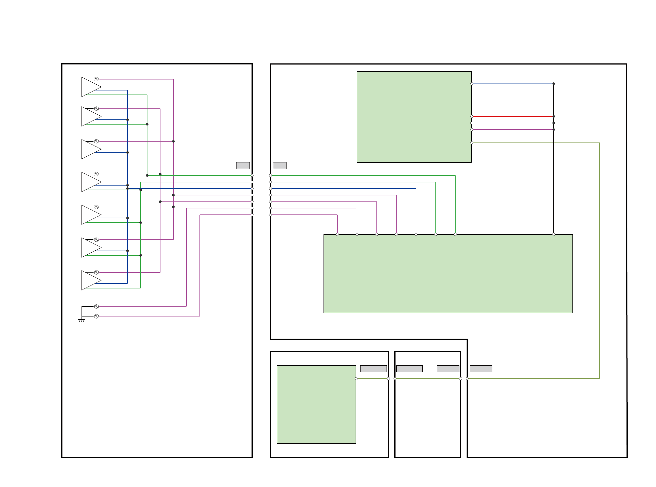
DIAGNOSTICPATHDIAGRAM
AVR-X3200W ANALOG VIDEO BLOCK
fig.01
CBL/SAT
CVBS IN
V.AUX(FRO NT)
CBL/SAT
COMPONENT IN
DVD
GAME
DVD
CBL/SAT _V
DVD_V
Blu-Ray_ V
V.AUX_V
75
75
NOT USED
NOT USED
CVBS M ONITOR
CVBS OUT
COMPO NENT OUT Y
CBL/SAT _Y
CBL/SAT _PB
CBL/SAT _PR
DVD_Y
DVD_PB
DVD_PR
CBL/SAT _Y
DVD_Y
CBL/SAT _PB
DVD_PB
CBL/SAT _PR
DVD_PR
V_AUX_V
CBL/SAT _V
DVD_V
Blu-Ray_V
NJM2595MTE1
VI1
VI2
VI3
VI4
VI5
0
AVRX3200
NJM2586AVC3
CH1 IN 1
CH1 IN 2
CH1 IN 3
CH2 IN 1
CH2 IN 2
CH2 IN 3
CH3 IN
CH3 IN 2
CH3 IN 3
SW1
SW2
SW3
SW4
SW5
VO1
VO2
75
AVRX3200
CH1 OU T
CH2 OU T
CH3 OU T
SW1
SW2
PS
YOUT
PBOUT
PROUT
75
6dB
75
6dB
75
6dB
1
AVR-X3200WBKE3 ONLY
COMPO NENT OUT PB
COMPO NENT OUT PR
COMPONENT OUT
DEC_CVB S_IN
DEC_Y_IN
DEC_PB_IN
DEC_PR_IN
HDMI BLOCK
28
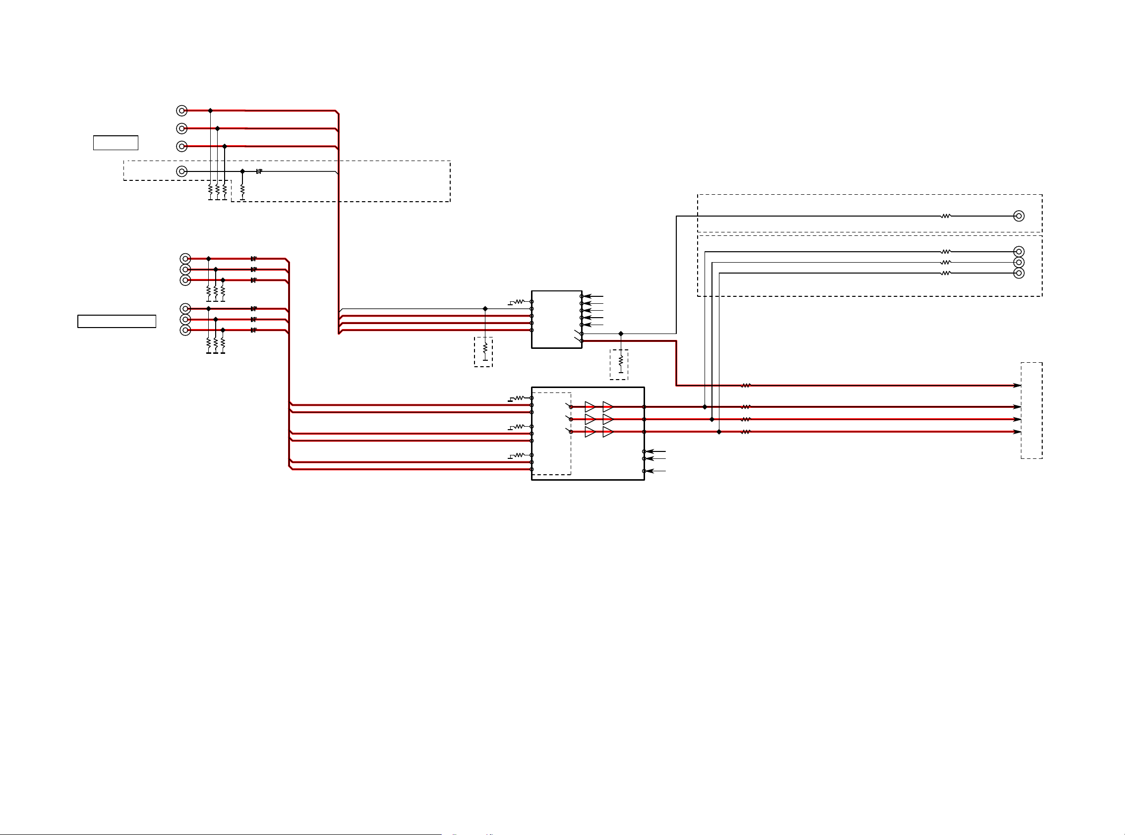
AVR-X3200W ANALOG VIDEO BLOCK
fig.02a
CVBS IN
V.AUX(FRO NT)
COMPONENT IN
CBL/SAT
DVD
GAME
CBL/SAT
DVD
CBL/SAT _V
DVD_V
Blu-Ray_ V
V.AUX_V
75
75
NOT USED
NOT USED
CVBS M ONITOR
CVBS OUT
COMPO NENT OUT Y
CBL/SAT _Y
CBL/SAT _PB
CBL/SAT _PR
DVD_Y
DVD_PB
DVD_PR
CBL/SAT _Y
DVD_Y
CBL/SAT _PB
DVD_PB
CBL/SAT _PR
DVD_PR
V_AUX_V
CBL/SAT _V
DVD_V
Blu-Ray_V
NJM2595MTE1
VI1
VI2
VI3
VI4
VI5
0
AVRX3200
NJM2586AVC3
CH1 IN 1
CH1 IN 2
CH1 IN 3
CH2 IN 1
CH2 IN 2
CH2 IN 3
CH3 IN
CH3 IN 2
CH3 IN 3
SW1
SW2
SW3
SW4
SW5
VO1
VO2
75
AVRX3200
CH1 OU T
CH2 OU T
CH3 OU T
SW1
SW2
PS
YOUT
PBOUT
PROUT
75
6dB
75
6dB
75
6dB
1
AVR-X3200WBKE3 ONLY
COMPO NENT OUT PB
COMPO NENT OUT PR
COMPONENT OUT
DEC_CVB S_IN
DEC_Y_IN
DEC_PB_IN
DEC_PR_IN
HDMI BLOCK
29
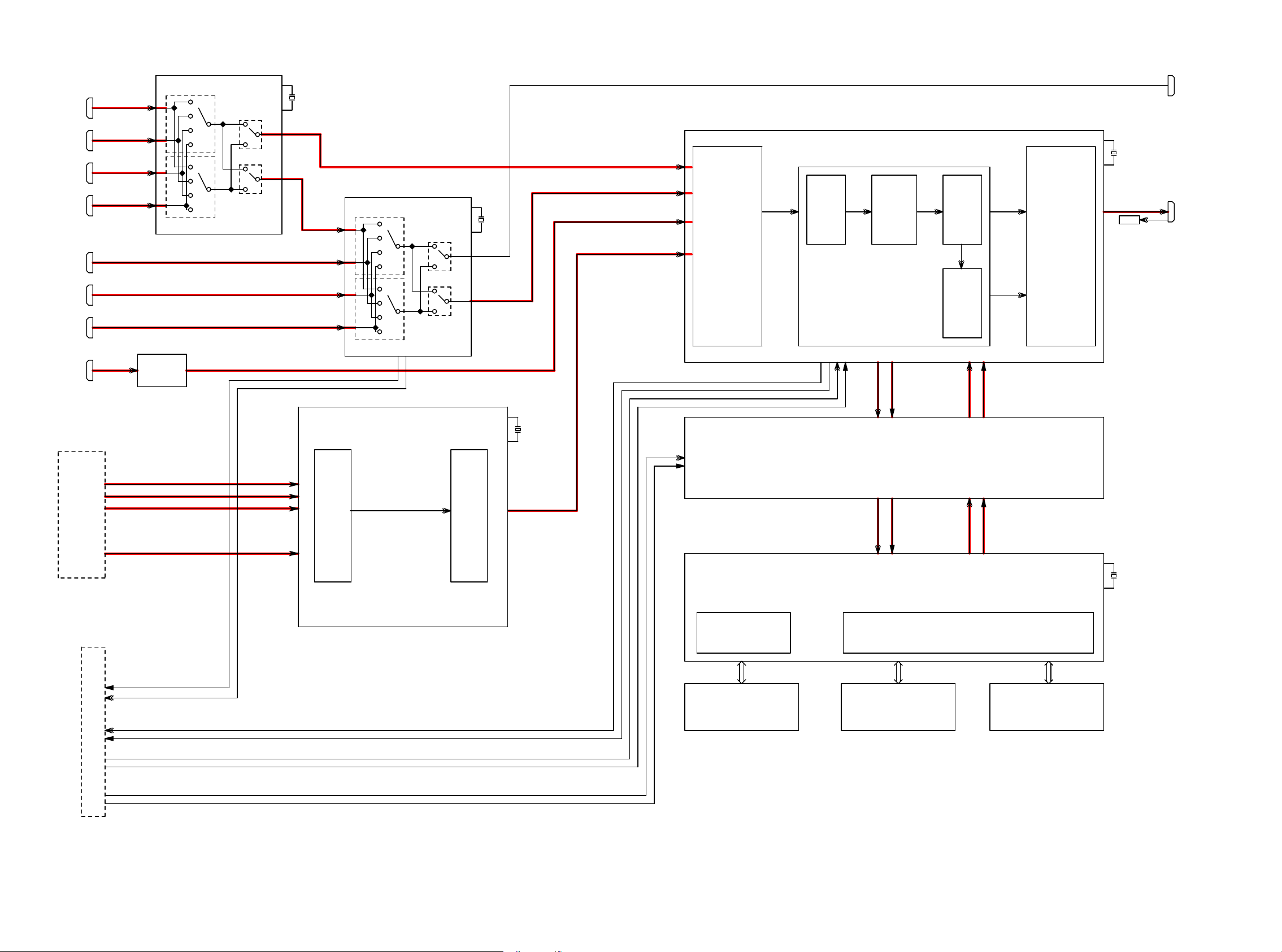
AVR-X3200W HDMI VIDEO BLOCK
HDMI I N1
(CBL/SA T)
HDMI I N2
(DVD)
HDMI I N3
(BLU- RAY)
HDMI I N4
(GAME)
HDMI I N5
(MEDIA Player)
HDMI I N6
(AUX2)
HDMI I N7
(CD)
HDMI I N8
(AUX1)
fig.02b
P3 RX
P2 RX
P1 RX
P0 RX
HDMI SW2(MN864788)
MAIN
AD8195
Buffer
SUB
DEC_Y_IN
DEC_PB_IN
DEC_PR_IN
27.000MHz
P0 TX
P1 TX
P3 RX
P2 RX
P1 RX
P0 RX
HDMI SW1(MN864788)
MAIN
SUB
105
119
ADV7850
27.000MHz
P0 TX
P1 TX
HDMI Z ONE2
P1 RX
HDMI TX(MN864787)
27.000MHz
P0 RX
HDMI Rx
P3 RX
600MHz
Rxlink0 Txlink0
Matrix SW
P2 RX
RXI2S0~3(DSD1 ~4), RXSPDIF(DSD0)
RXMCK(DS DMCK), RXBCK (DSDSCK), RXLRCK (DSD5), RXINT0
27.000MHz
870VD0~7
870PCK
TXI2S0
TXBCK , TXLRCK
VIDEO PLD
EPM570F256C4N
4K/2K
Up Scaler
B0~B7 /G0~G7/R0~R7
PCK/HSYN C/VSYNC/DE
Txlink1
B0~B7 /G0~G7/R0~R7
YNC/DE
PCK/HSYN C/VS
600MHz
4K/2K
600MHz
4K/2K
HDMI Tx
Matrix SW
P1 TX
ARC
HDMI O UT1
ANALOG
VIDEO BLOCK
Z2_HAINT
Z2HDMISP DIF
RXI2S0~3(DSD1 ~4), RXSPDIF(DSD0)
RXMCK(DS DMCK), RXBCK (DSDSCK), RXLRCK (DSD5), RXINT0
TXI2S0
TXBCK , TXLRCK
870VD0~7
870PCK
DIGITAL AUDIO BLOCK
DEC_CVB S_IN
WITH TMDS
B0~B7 /G0~G7/R0~R7
VIDEO INPUT
VIDEO SIGNAL OUT
PCK/HSYN C/VSYNC/DE
B0~B7 /G0~G7/R0~R7
PCK/HSYN C/VSYNC/DE
AD55/058Z-0(ADV8003-8B)
Video Processor(1080P, OSD, IP Conv,)
CONTROL
S. FLASH
MX25L12845EMI-10G
128M
DDR2 SDRAM
A3R12E40CBF-8E A3R12E40CBF-8E
512M
DDR2 INTERFACE
DDR2 SDRAM
512M
27.000MHz
30

AVR-X3200W HDMI VIDEO BLOCK
HDMI I N1
(CBL/SA T)
HDMI I N2
(DVD)
HDMI I N3
(BLU- RAY)
HDMI I N4
(GAME)
HDMI I N5
(MEDIA Player)
HDMI I N6
(AUX2)
HDMI I N7
(CD)
HDMI I N8
(AUX1)
fig.03
P3 RX
P2 RX
P1 RX
P0 RX
HDMI SW2(MN864788)
MAIN
AD8195
Buffer
SUB
DEC_Y_IN
DEC_PB_IN
DEC_PR_IN
27.000MHz
P0 TX
P1 TX
P3 RX
P2 RX
P1 RX
P0 RX
HDMI SW1(MN864788)
MAIN
SUB
105
119
ADV7850
27.000MHz
P0 TX
P1 TX
HDMI Z ONE2
P1 RX
HDMI TX(MN864787)
27.000MHz
P0 RX
HDMI Rx
P3 RX
600MHz
Rxlink0 Txlink0
Matrix SW
P2 RX
RXI2S0~3(DSD1 ~4), RXSPDIF(DSD0)
RXMCK(DS DMCK), RXBCK (DSDSCK), RXLRCK (DSD5), RXINT0
27.000MHz
870VD0~7
870PCK
TXI2S0
TXBCK , TXLRCK
VIDEO PLD
EPM570F256C4N
4K/2K
Up Scaler
B0~B7 /G0~G7/R0~R7
PCK/HSYN C/VSYNC/DE
Txlink1
B0~B7 /G0~G7/R0~R7
YNC/DE
PCK/HSYN C/VS
600MHz
4K/2K
600MHz
4K/2K
HDMI Tx
Matrix SW
P1 TX
ARC
HDMI O UT1
ANALOG
VIDEO BLOCK
Z2_HAINT
Z2HDMISP DIF
RXI2S0~3(DSD1 ~4), RXSPDIF(DSD0)
RXMCK(DS DMCK), RXBCK (DSDSCK), RXLRCK (DSD5), RXINT0
TXI2S0
TXBCK , TXLRCK
870VD0~7
870PCK
DIGITAL AUDIO BLOCK
DEC_CVB S_IN
WITH TMDS
B0~B7 /G0~G7/R0~R7
VIDEO INPUT
VIDEO SIGNAL OUT
PCK/HSYN C/VSYNC/DE
B0~B7 /G0~G7/R0~R7
PCK/HSYN C/VSYNC/DE
AD55/058Z-0(ADV8003-8B)
Video Processor(1080P, OSD, IP Conv,)
CONTROL
S. FLASH
MX25L12845EMI-10G
128M
DDR2 SDRAM
A3R12E40CBF-8E A3R12E40CBF-8E
512M
DDR2 INTERFACE
DDR2 SDRAM
512M
27.000MHz
31

AVR-X3200W HDMI VIDEO BLOCK
HDMI I N1
(CBL/SA T)
HDMI I N2
(DVD)
HDMI I N3
(BLU- RAY)
HDMI I N4
(GAME)
HDMI I N5
(MEDIA Player)
HDMI I N6
(AUX2)
HDMI I N7
(CD)
HDMI I N8
(AUX1)
fig.04
P3 RX
P2 RX
P1 RX
P0 RX
HDMI SW2(MN864788)
MAIN
AD8195
Buffer
SUB
DEC_Y_IN
DEC_PB_IN
DEC_PR_IN
27.000MHz
P0 TX
P1 TX
P3 RX
P2 RX
P1 RX
P0 RX
HDMI SW1(MN864788)
MAIN
SUB
105
119
ADV7850
27.000MHz
P0 TX
P1 TX
HDMI Z ONE2
uCOM
27.000MHz
P1 RX
HDMI TX(MN864787)
P0 RX
HDMI Rx
P3 RX
600MHz
Rxlink0 Txlink0
Matrix SW
P2 RX
RXI2S0~3(DSD1 ~4), RXSPDIF(DSD0)
RXMCK(DS DMCK), RXBCK (DSDSCK), RXLRCK (DSD5), RXINT0
27.000MHz
870VD0~7
870PCK
TXI2S0
TXBCK , TXLRCK
VIDEO PLD
EPM570F256C4N
4K/2K
Up Scaler
B0~B7 /G0~G7/R0~R7
PCK/HSYN C/VSYNC/DE
Txlink1
B0~B7 /G0~G7/R0~R7
YNC/DE
PCK/HSYN C/VS
600MHz
4K/2K
600MHz
4K/2K
HDMI Tx
Matrix SW
P1 TX
ARC
HDMI O UT1
ANALOG
VIDEO BLOCK
Z2_HAINT
Z2HDMISP DIF
RXI2S0~3(DSD1 ~4), RXSPDIF(DSD0)
RXMCK(DS DMCK), RXBCK (DSDSCK), RXLRCK (DSD5), RXINT0
TXI2S0
TXBCK , TXLRCK
870VD0~7
870PCK
DIGITAL AUDIO BLOCK
DEC_CVB S_IN
WITH TMDS
B0~B7 /G0~G7/R0~R7
VIDEO INPUT
VIDEO SIGNAL OUT
PCK/HSYN C/VSYNC/DE
B0~B7 /G0~G7/R0~R7
PCK/HSYN C/VSYNC/DE
AD55/058Z-0(ADV8003-8B)
Video Processor(1080P, OSD, IP Conv,)
CONTROL
S. FLASH
MX25L12845EMI-10G
128M
DDR2 SDRAM
A3R12E40CBF-8E A3R12E40CBF-8E
512M
DDR2 INTERFACE
DDR2 SDRAM
512M
27.000MHz
32

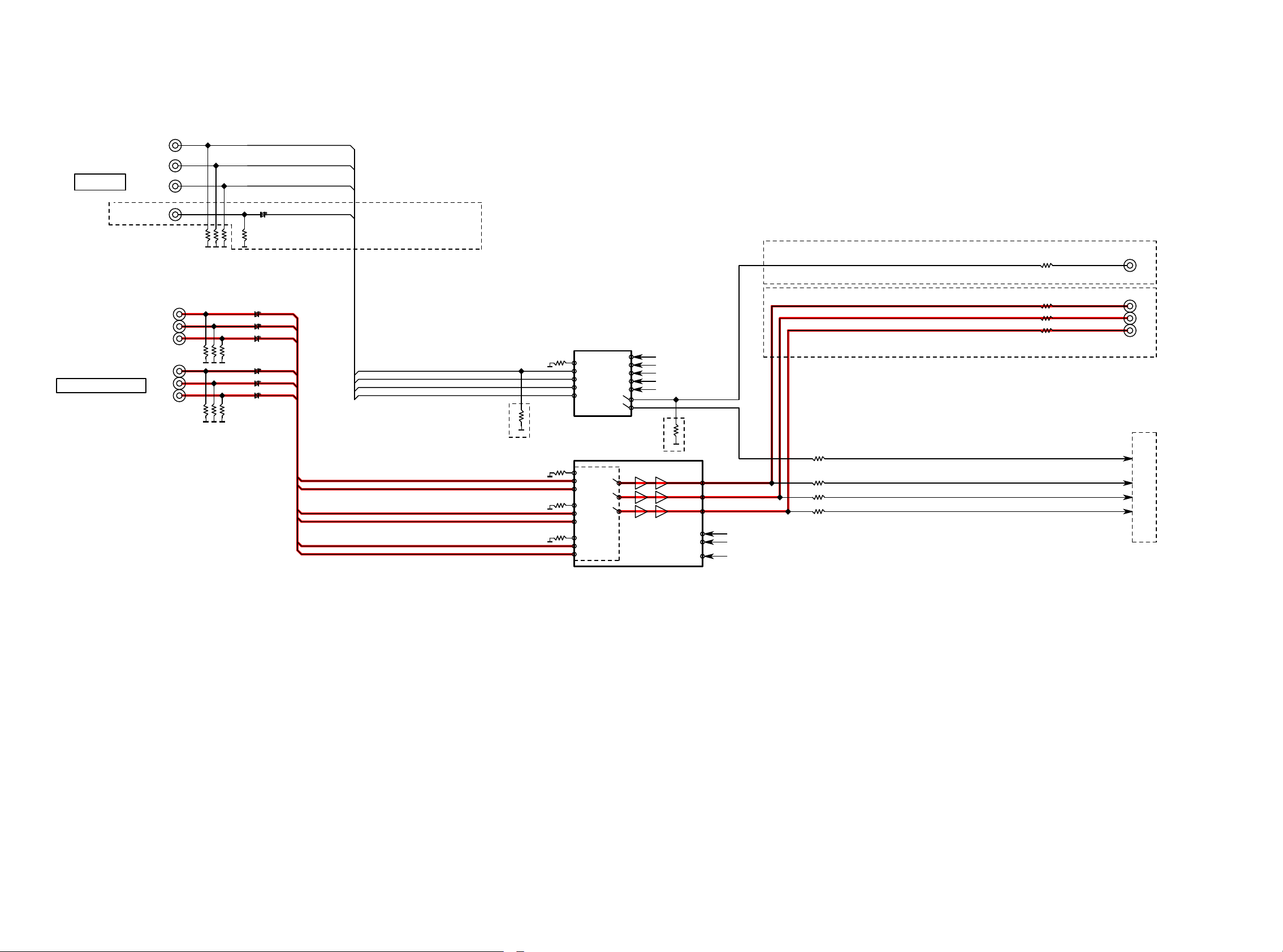
AVR-X3200W ANALOG AUDIO BLOCK
CBL/SAT
DVD
Blu-Ray
Media
PHONO
V.AUX
(FRONT)
CD
MIC
AVR-X4200W
TUNER
TUNER(FM/AM)
DAZ2
DAZ3
ADINL
ADINR
DAFL
DAFR
DAC
DASW1
DASW2
DASL
DASR
DAASSIGN1L
DAASSIGN1R
DAASSIGN2L
DAASSIGN2R
DIGITAL AUDIO BLOCK_C1
DAC_F
70,71
72.73
74,75
76,77
78,79
82,83
64,65
66,67
62,63
68.69
60,61
58,59
56,57
84,85
MAIN ZONE SWZONE2 SWZONE3 SW
HPF
MONO
MIX
HPF
HPF
MONO
MIX
HPF
ZONE3
Only AVR-X4200X
ADC
SUB_2
53,54
32,33
ZONE3
MONO
MIX
MONO
MIX
R2A15220
MAIN_Front
SUB_1
46,47
80,81
88,89
ZONE2
BD3841F
1
7
3
5
2
8
4
6
9
15
11
13
10
16
12
14
34,35
26
25
20
19
fig.05a
Z2 IN2(HPF/MONO)
42,43
90,91
ZONE2
ZONE2
ZONE2ZONE3
Z2 IN1
DAASSIGN1L
(SB1/FH1/FW1)
DAASSIGN1R
(SB1/FH1/FW1)
DASW2
DASW1
DAFL
ANA_L
DAFR
ANA_R
ZONE3
ZONE3
DAC
42,43
93,94
Z3 IN2(HPF/MONO)
38
39
Z3 IN1
TONE
TONE
TONE
TONE
19,20
22,23
16
7,8
10,11
99,100
2,3
Z2L_VOL_OUT
Z2R_VOL_OUT
FL_VOL_OUT
FR_VOL_OUT
C_VOL_OUT
SW1_VOL_OUT
SW2_VOL_OUT
SL_VOL_OUT
SR_VOL_OUT
ASSIGN1L_VOL_OUT
ASSIGN1R_VOL_OUT
ASSIGN2L_VOL_OUT
ASSIGN2R_VOL_OUT
ASSIGN1L
ASSIGN1R
ASSIGN2L
ASSIGN2R
Z3R_VOL_OUT
Z3L_VOL_OUT
21
23
SR_VOL_OUT
SW1_VOL_OUT
SW2_VOL_OUT
SL_VOL_OUT
9
15
17
11
ASSIGN2R_VOL_OUT
ASSIGN2L_VOL_OUT
3
5
ASSIGN1L
ASSIGN1R
ASSIGN2L
ASSIGN2R
696871
70
FLFRZ2L
Z2R
CSLSR
CSLSR
FLFRZ2L
Z2R
66
79
78
72,73
Z3L
Z3R
PREOUT_FL
PREOUT_FR
PREOUT_C
PREOUT_SW1
PREOUT_SW2
PREOUT_SL
PREOUT_SR
PREOUT_ASS1L
PREOUT_ASS1R
PREOUT_ASS2L
PREOUT_ASS2R
Z2_MONO
Z3_MONO
60615859636267
FL
FR
C
SW1
SW2
SL
SR
InA1
InB1
InA2
InB2
SW-A x 4
InA3
InB3
InA4
SW-B x 4
InB4
NJU72751
Z2L
Z2R
Z3L
Z3R
C
SL
SR
Only AVR-X4200W
POWER AMP PART
29dB
29dB
29dB
29dB
tceleS PMA tnorFtceleS PMA BS
46
47
SUB
29dB
29dB
29dB
OutA1
OutB1
OutA2
OutB2
OutA3
OutB3
OutA4
OutB4
V
SBL
SBR
FW_L
FW_R
H1_L
H1_R
H2_L
H2_R
Only AVR-X4200W
ZONE2 OUT
ZONE2 OUT
ZONE3 OUT
ATT.
ZONE3 OUT
HPL
HPR
H/P OUT
GND
FL
ZONE3
RY921
FR
RY922
RY923
C
SL
SR
RY924
SBL
RY927
RY925
SBR
FW_L
DASL
DASR
DAASSIGN2L
(SB2/FH2/FW2)
DAASSIGN2R
(SB2/FH2/FW2)
40
RY928
RY926
FW_R
H_L
41
36
37
91
REC3
90
Only AVR-X4200W
H_R
R2A15218
33

AVR-X3200W DIGITAL AUDIO BLOCK
OPT1(TV)
OPT2(CD)
COAX1(CBL/SAT)
COAX2(DVD)
DENON_LINK
AVRX4200 ONLY
fig.05b
DIGTAL IN
ANT1
ANT2
USB
ETHERNET
RJ-45 with Transformer
HDMI BLOCK_A6
USBD-
USBD+
Z2HDMISPDIF
USB
BD82065FVJ-E2
RX+/-
TX+/-
920VD0~7
920PCK
to MAIN DIR #28
RXMCK/DSDMCK
RXBCK/DSDSCK
RXLRCK/DSD5
RXI2S0/DSD1
RXI2S1/DSD2
RXI2S2/DSD3
RXI2S3/DSD4
RXSPDIF/DSD0
RXINT0
TO MAIN CPU #147
TXBCK
TXLRCK
TXI2S0
Z2_HAINT
CY920
NETWORKED
MEDIA MODULE
IPOD AUTH.
23671011050AS
(MFI337S3959)
A2
A4
B3
B4
C2
C3
C4
B1
D4
K1
K2
L1
E1
OPT.0
OPT.1
COAX.0
COAX.1
SERIAL FLASH
256M
MX25L25635FMI-10G
#33
#32
#37
#35
(To MAIN DIR)
BCOSPDIF
DENONLINKHD
to MAIN DIR #31
BCOMCK
BCOBCK_SCK
BCOLRCK
BCODATA_DSDL
BCODSDR
AVR-X4200W
Z3DIRSPDIF
ZONE3 DIR
(To Z3 DAC #10)
#89
E3
LC89091JA-H
13591011124
DEMPZ3
(To Z2 DAC #10)
3
Z3DIRPERR
Z3DIRnPCM
Z3DIRDATA
Z3DIRBCK
Z3DIRLRCK
Z3DIRMCK
F16
F15
G16
G15
G14
H14
66
DEMPZ2
(To MAIN CPU)
(From LEVEL_CHG)
#9(LEVEL_CHG), N4(V.PLD)
#L6 (To V.PLD)
#3(LEVEL_CHG), P3(V.PLD)
#7(LEVEL_CHG)
JTAG_TDI
TDO1_TDI2
JTAG_TCK
JTAG_TMS
APLD_DI
L6
P3
N4
M5
C12
J1
J2
H1
H2
K3
#104
#102
#14
#12
#16
Z3PLDAERR
Z2PLDAERR
PLDAERR
APLD_CS
APLD_CK
L2
F1
G2
G1
M1
Z2DIRSPDIF
ZONE2 DIR
LC89091JA-H
13591011124
Z2DIRDATA
Z2DIRBCK
Z2DIRLRCK
Z2DIRMCK
J16
J15
H16
H15
COAX.0
COAX.1
OPT.0
OPT.1
BCOSPDIF
Z2HDMISPDIF
3
Z2DIRPERR
Z2DIRnPCM
J14
J12
24.576MHz
37
35
33
32
31
28
29, 30
789
DIRAUXDATA
DIRAUXLRCK
DIRAUXBCK
DIRAUXMCK
HDMISPDIF
L16
K14
K15
H12
ADINL
ADINR
15
16
48
47
DIR + ADC
PCM9211PTR
52019181721
10
DIRXMCK
DIRDATA
DIRBCK
DIRLRCK
DIRMCK
L15
K16
N15
N16
M15
3426242325
DIRPERR
DIRnPCM
L14
M16
L13
AUDIO PLD
5M570ZF256C5N
21A85
11C95
11A06
01C26
01B46
11B36
7C64 ,72
6C65
6A44 ,62
8C54
8A32
7A22
5B91
8B81
6B71
E485, 88
5C61
9B75
9A16
51A17
9C27
A5
14
13
12
11
3
4
DIRSBCK
DIRSLRCK
E16
D16
P5
N5
P4
P7
P2
R1
N1
N3
P6
N2
M2
M3
R16
R12
P12
N12
R14
T15
T12
R13
P13
T13
N14
M14
M13
N13
P11
P14
P15
DIRRST
DIRCE
DIRDIN
DIRDOUT
DIRCLK
DATAAD
DIRADLRCK
DIRADBCK
DIRADMCK
#101
#100
#98
#99
(From MAINCPU)
DACMCK
DACBCK
DACLRCK
DZF1
DACPCMF
DACPCMCSW1
DACPCMSW2RSV
DACPCMS
DACPCMASSIGN3(OPEN)
DACRST
DACMS
DACMDI
DACMC
DACMCK
DACBCK
DACLRCK
DZF2
DACPCMASSIGN1
DACPCMASSIGN2
(From Z2 DIR #6)
Z2DACMCK
Z2DACBCK
Z2DACLRCK
Z2DACDATA
Z2DACMUTE
(From Z3 DIR #6)
Z3DACMCK
Z3DACBCK
Z3DACLRCK
Z3DACDATA
Z3DACMUTE
CSCKOUT
CSCLOCK
#146
#143
#141
#144
#145
CSCKIN
CSREFIN
CSSCL
CSSDA
#128
(From/To MAINCPU)
9
10
12
AK5358BET
11
48/15
15/22
13/20
14/21
1/14
2/7
3/6
11/16
4/11
5/10
7/8
6/9
48/15
15/22
13/20
14/21
1/14
2/7
3/6
11/16
4/10
5/9
6/8
10
12
13
15
14
17
10
12
13
15
14
17
3
4
5
7
CSCS
CS210010-CZZR
8
9
10
ADCRST
(From MAINCPU)
13
ADC
MAIN DAC1
PIN NO :
AK4458/PCM1690
AK4458
PCM1690
(AVRX3200W)
(AVRX4200W)
MAIN DAC2
PIN NO :
AK4458/PCM1690
AK4458
PCM1690
(AVRX3200W)
(AVR4200W)
ZONE2
DAC
PCM5100
ZONE3
DAC
PCM5100
JITTER
REDUCER
AVR-X4200W
2
1
18/31
19/32
23/29
22/30
24/35
25/36
29/33
28/34
38/43
39/44
43/41
42/42
32/39
33/40
37/37
36/38
18/35
19/36
23/33
22/34
24/39
25/40
29/37
28/38
32/43
33/44
37/41
36/42
ADINL
ADINR
DAFL
DAFR
DAC
DASW1
DASW2
DARSV
DASL
DASR
DAASSIGN1L
DAASSIGN1R
DAASSIGN2L
DAASSIGN2R
DAASSIGN3L
DAASSIGN3R
OPEN
6
7
DAZ2L
DAZ2R
ANALOG AUDIO BLOCK_B6
6
7
DAZ3L
DAZ3R
24.576 MHz
DSP1INSWC_C
DSP1INS_SL
DSP1INF_FL
DSP1INLR
DSP1INBCK
DSP1INLRCK
DSP1INMCK
PLDAERR2
DSP1INRSV_SW
DSP1INSB_SR
DSP1INRSV_FR
DSP1OUTBCK
DSP1OUTSB
DSP1OUTS
DSP1OUTCSW1
DSP1OUTF
DSP1OUTLRCK
DSP1OUTFW
DSP1OUTFH
DSP
CIRRUS LOGIC CS49844A(QUAD-CORE)
FLASHSDRAM
M12L64164A-5TG2Y
64M64M
MX25L6406EM2I-12G
34
DSP1OUTRSV1
DSP1FLAG3
DSP1OUTRSW2
87
817532
DSPICS
DSP1FLAG0
DSPRST
#83
#84
#82
(From/To MAIN CPU)
AVR-X4200W
DSP1FLAG3
#176

AVR-X3200W HDMI VIDEO BLOCK
HDMI I N1
(CBL/SA T)
HDMI I N2
(DVD)
HDMI I N3
(BLU- RAY)
HDMI I N4
(GAME)
HDMI I N5
(MEDIA Player)
HDMI I N6
(AUX2)
HDMI I N7
(CD)
HDMI I N8
(AUX1)
fig.05c
P3 RX
P2 RX
P1 RX
P0 RX
HDMI SW2(MN864788)
MAIN
AD8195
Buffer
SUB
DEC_Y_IN
DEC_PB_IN
DEC_PR_IN
27.000MHz
P0 TX
P1 TX
P3 RX
P2 RX
P1 RX
P0 RX
HDMI SW1(MN864788)
MAIN
SUB
105
119
ADV7850
27.000MHz
P0 TX
P1 TX
HDMI Z ONE2
P1 RX
HDMI TX(MN864787)
27.000MHz
P0 RX
HDMI Rx
P3 RX
600MHz
Rxlink0 Txlink0
Matrix SW
P2 RX
RXI2S0~3(DSD1 ~4), RXSPDIF(DSD0)
RXMCK(DS DMCK), RXBCK (DSDSCK), RXLRCK (DSD5), RXINT0
27.000MHz
870VD0~7
870PCK
TXI2S0
TXBCK , TXLRCK
VIDEO PLD
EPM570F256C4N
4K/2K
Up Scaler
B0~B7 /G0~G7/R0~R7
PCK/HSYN C/VSYNC/DE
Txlink1
B0~B7 /G0~G7/R0~R7
YNC/DE
PCK/HSYN C/VS
600MHz
4K/2K
600MHz
4K/2K
HDMI Tx
Matrix SW
P1 TX
ARC
HDMI O UT1
ANALOG
VIDEO BLOCK
Z2_HAINT
Z2HDMISP DIF
RXI2S0~3(DSD1 ~4), RXSPDIF(DSD0)
RXMCK(DS DMCK), RXBCK (DSDSCK), RXLRCK (DSD5), RXINT0
TXI2S0
TXBCK , TXLRCK
870VD0~7
870PCK
DIGITAL AUDIO BLOCK
DEC_CVB S_IN
WITH TMDS
B0~B7 /G0~G7/R0~R7
VIDEO INPUT
VIDEO SIGNAL OUT
PCK/HSYN C/VSYNC/DE
B0~B7 /G0~G7/R0~R7
PCK/HSYN C/VSYNC/DE
AD55/058Z-0(ADV8003-8B)
Video Processor(1080P, OSD, IP Conv,)
CONTROL
S. FLASH
MX25L12845EMI-10G
128M
DDR2 SDRAM
A3R12E40CBF-8E A3R12E40CBF-8E
512M
DDR2 INTERFACE
DDR2 SDRAM
512M
27.000MHz
35

AVR-X3200W DIGITAL AUDIO BLOCK
OPT1(TV)
OPT2(CD)
COAX1(CBL/SAT)
COAX2(DVD)
DENON_LINK
AVRX4200 ONLY
fig.06a
DIGTAL IN
ANT1
ANT2
USB
ETHERNET
RJ-45 with Transformer
HDMI BLOCK_A6
USBD-
USBD+
Z2HDMISPDIF
USB
BD82065FVJ-E2
RX+/-
TX+/-
920VD0~7
920PCK
to MAIN DIR #28
RXMCK/DSDMCK
RXBCK/DSDSCK
RXLRCK/DSD5
RXI2S0/DSD1
RXI2S1/DSD2
RXI2S2/DSD3
RXI2S3/DSD4
RXSPDIF/DSD0
RXINT0
TO MAIN CPU #147
TXBCK
TXLRCK
TXI2S0
Z2_HAINT
CY920
NETWORKED
MEDIA MODULE
IPOD AUTH.
23671011050AS
(MFI337S3959)
A2
A4
B3
B4
C2
C3
C4
B1
D4
K1
K2
L1
E1
OPT.0
OPT.1
COAX.0
COAX.1
SERIAL FLASH
256M
MX25L25635FMI-10G
#33
#32
#37
#35
(To MAIN DIR)
BCOSPDIF
DENONLINKHD
to MAIN DIR #31
BCOMCK
BCOBCK_SCK
BCOLRCK
BCODATA_DSDL
BCODSDR
AVR-X4200W
Z3DIRSPDIF
ZONE3 DIR
(To Z3 DAC #10)
#89
E3
LC89091JA-H
13591011124
DEMPZ3
(To Z2 DAC #10)
3
Z3DIRPERR
Z3DIRnPCM
Z3DIRDATA
Z3DIRBCK
Z3DIRLRCK
Z3DIRMCK
F16
F15
G16
G15
G14
H14
66
DEMPZ2
(To MAIN CPU)
(From LEVEL_CHG)
#9(LEVEL_CHG), N4(V.PLD)
#L6 (To V.PLD)
#3(LEVEL_CHG), P3(V.PLD)
#7(LEVEL_CHG)
JTAG_TDI
TDO1_TDI2
JTAG_TCK
JTAG_TMS
APLD_DI
L6
P3
N4
M5
C12
J1
J2
H1
H2
K3
#104
#102
#14
#12
#16
Z3PLDAERR
Z2PLDAERR
PLDAERR
APLD_CS
APLD_CK
L2
F1
G2
G1
M1
Z2DIRSPDIF
ZONE2 DIR
LC89091JA-H
13591011124
Z2DIRDATA
Z2DIRBCK
Z2DIRLRCK
Z2DIRMCK
J16
J15
H16
H15
COAX.0
COAX.1
OPT.0
OPT.1
BCOSPDIF
Z2HDMISPDIF
3
Z2DIRPERR
Z2DIRnPCM
J14
J12
24.576MHz
37
35
33
32
31
28
29, 30
789
DIRAUXDATA
DIRAUXLRCK
DIRAUXBCK
DIRAUXMCK
HDMISPDIF
L16
K14
K15
H12
ADINL
ADINR
15
16
48
47
DIR + ADC
PCM9211PTR
52019181721
10
DIRXMCK
DIRDATA
DIRBCK
DIRLRCK
DIRMCK
L15
K16
N15
N16
M15
3426242325
DIRPERR
DIRnPCM
L14
M16
L13
AUDIO PLD
5M570ZF256C5N
21A85
11C95
11A06
01C26
01B46
11B36
7C64 ,72
6C65
6A44 ,62
8C54
8A32
7A22
5B91
8B81
6B71
E485, 88
5C61
9B75
9A16
51A17
9C27
A5
14
13
12
11
3
4
DIRSBCK
DIRSLRCK
E16
D16
P5
N5
P4
P7
P2
R1
N1
N3
P6
N2
M2
M3
R16
R12
P12
N12
R14
T15
T12
R13
P13
T13
N14
M14
M13
N13
P11
P14
P15
DIRRST
DIRCE
DIRDIN
DIRDOUT
DIRCLK
DATAAD
DIRADLRCK
DIRADBCK
DIRADMCK
#101
#100
#98
#99
(From MAINCPU)
DACMCK
DACBCK
DACLRCK
DZF1
DACPCMF
DACPCMCSW1
DACPCMSW2RSV
DACPCMS
DACPCMASSIGN3(OPEN)
DACRST
DACMS
DACMDI
DACMC
DACMCK
DACBCK
DACLRCK
DZF2
DACPCMASSIGN1
DACPCMASSIGN2
(From Z2 DIR #6)
Z2DACMCK
Z2DACBCK
Z2DACLRCK
Z2DACDATA
Z2DACMUTE
(From Z3 DIR #6)
Z3DACMCK
Z3DACBCK
Z3DACLRCK
Z3DACDATA
Z3DACMUTE
CSCKOUT
CSCLOCK
#146
#143
#141
#144
#145
CSCKIN
CSREFIN
CSSCL
CSSDA
#128
(From/To MAINCPU)
9
10
12
AK5358BET
11
48/15
15/22
13/20
14/21
1/14
2/7
3/6
11/16
4/11
5/10
7/8
6/9
48/15
15/22
13/20
14/21
1/14
2/7
3/6
11/16
4/10
5/9
6/8
10
12
13
15
14
17
10
12
13
15
14
17
3
4
5
7
CSCS
CS210010-CZZR
8
9
10
ADCRST
(From MAINCPU)
13
ADC
MAIN DAC1
PIN NO :
AK4458/PCM1690
AK4458
PCM1690
(AVRX3200W)
(AVRX4200W)
MAIN DAC2
PIN NO :
AK4458/PCM1690
AK4458
PCM1690
(AVRX3200W)
(AVR4200W)
ZONE2
DAC
PCM5100
ZONE3
DAC
PCM5100
JITTER
REDUCER
AVR-X4200W
2
1
18/31
19/32
23/29
22/30
24/35
25/36
29/33
28/34
38/43
39/44
43/41
42/42
32/39
33/40
37/37
36/38
18/35
19/36
23/33
22/34
24/39
25/40
29/37
28/38
32/43
33/44
37/41
36/42
ADINL
ADINR
DAFL
DAFR
DAC
DASW1
DASW2
DARSV
DASL
DASR
DAASSIGN1L
DAASSIGN1R
DAASSIGN2L
DAASSIGN2R
DAASSIGN3L
DAASSIGN3R
OPEN
6
7
DAZ2L
DAZ2R
ANALOG AUDIO BLOCK_B6
6
7
DAZ3L
DAZ3R
24.576 MHz
DSP1INSWC_C
DSP1INS_SL
DSP1INF_FL
DSP1INLR
DSP1INBCK
DSP1INLRCK
DSP1INMCK
PLDAERR2
DSP1INRSV_SW
DSP1INSB_SR
DSP1INRSV_FR
DSP1OUTBCK
DSP1OUTSB
DSP1OUTS
DSP1OUTCSW1
DSP1OUTF
DSP1OUTLRCK
DSP1OUTFW
DSP1OUTFH
DSP
CIRRUS LOGIC CS49844A(QUAD-CORE)
FLASHSDRAM
M12L64164A-5TG2Y
64M64M
MX25L6406EM2I-12G
36
DSP1OUTRSV1
DSP1FLAG3
DSP1OUTRSW2
87
817532
DSPICS
DSP1FLAG0
DSPRST
#83
#84
#82
(From/To MAIN CPU)
AVR-X4200W
DSP1FLAG3
#176

AVR-X3200W HDMI VIDEO BLOCK
HDMI I N1
(CBL/SA T)
HDMI I N2
(DVD)
HDMI I N3
(BLU- RAY)
HDMI I N4
(GAME)
HDMI I N5
(MEDIA Player)
HDMI I N6
(AUX2)
HDMI I N7
(CD)
HDMI I N8
(AUX1)
fig.06b
P3 RX
P2 RX
P1 RX
P0 RX
HDMI SW2(MN864788)
MAIN
AD8195
Buffer
SUB
DEC_Y_IN
DEC_PB_IN
DEC_PR_IN
27.000MHz
P0 TX
P1 TX
P3 RX
P2 RX
P1 RX
P0 RX
HDMI SW1(MN864788)
MAIN
SUB
105
119
ADV7850
27.000MHz
P0 TX
P1 TX
HDMI Z ONE2
P1 RX
HDMI TX(MN864787)
27.000MHz
P0 RX
HDMI Rx
P3 RX
600MHz
Rxlink0 Txlink0
Matrix SW
P2 RX
RXI2S0~3(DSD1 ~4), RXSPDIF(DSD0)
RXMCK(DS DMCK), RXBCK (DSDSCK), RXLRCK (DSD5), RXINT0
27.000MHz
870VD0~7
870PCK
TXI2S0
TXBCK , TXLRCK
VIDEO PLD
EPM570F256C4N
4K/2K
Up Scaler
B0~B7 /G0~G7/R0~R7
PCK/HSYN C/VSYNC/DE
Txlink1
B0~B7 /G0~G7/R0~R7
YNC/DE
PCK/HSYN C/VS
600MHz
4K/2K
600MHz
4K/2K
HDMI Tx
Matrix SW
P1 TX
ARC
HDMI O UT1
ANALOG
VIDEO BLOCK
Z2_HAINT
Z2HDMISP DIF
RXI2S0~3(DSD1 ~4), RXSPDIF(DSD0)
RXMCK(DS DMCK), RXBCK (DSDSCK), RXLRCK (DSD5), RXINT0
TXI2S0
TXBCK , TXLRCK
870VD0~7
870PCK
DIGITAL AUDIO BLOCK
DEC_CVB S_IN
WITH TMDS
B0~B7 /G0~G7/R0~R7
VIDEO INPUT
VIDEO SIGNAL OUT
PCK/HSYN C/VSYNC/DE
B0~B7 /G0~G7/R0~R7
PCK/HSYN C/VSYNC/DE
AD55/058Z-0(ADV8003-8B)
Video Processor(1080P, OSD, IP Conv,)
CONTROL
S. FLASH
MX25L12845EMI-10G
128M
DDR2 SDRAM
A3R12E40CBF-8E A3R12E40CBF-8E
512M
DDR2 INTERFACE
DDR2 SDRAM
512M
27.000MHz
37

AVR-X3200W HDMI VIDEO BLOCK
HDMI I N1
(CBL/SA T)
H
DMI I N2
(DVD)
HDMI I N3
(BLU- RAY)
HDMI I N4
(GAME)
HDMI I N5
(MEDIA Player)
HDMI I N6
(AUX2)
HDMI I N7
(CD)
HDMI I N8
(AUX1)
fig.07
P3 RX
P2 RX
P1 RX
P0 RX
HDMI SW2(MN864788)
MAIN
AD8195
Buffer
SUB
DEC_Y_IN
DEC_PB_IN
DEC_PR_IN
27.000MHz
P0 TX
P1 TX
P3 RX
P2 RX
P1 RX
P0 RX
HDMI SW1(MN864788)
MAIN
SUB
105
119
ADV7850
27.000MHz
P0 TX
P1 TX
HDMI Z ONE2
P1 RX
HDMI TX(MN864787)
27.000MHz27.000MHz
P0 RX
HDMI Rx
P3 RX
600MHz
Rxlink0 Txlink0
Matrix SW
P2 RX
RXI2S0~3(DSD1 ~4), RXSPDIF(DSD0)
RXMCK(DS DMCK), RXBCK (DSDSCK), RXLRCK (DSD5), RXINT0
27.000MHz
870VD0~7
870PCK
TXI2S0
TXBCK , TXLRCK
VIDEO PLD
EPM570F256C4N
4K/2K
Up Scaler
B0~B7 /G0~G7/R0~R7
PCK/HSYN C/VSYNC/DE
Txlink1
B0~B7 /G0~G7/R0~R7
PCK/HSYN C/VSYNC/DE
600MHz
4K/2K
600MHz
4K/2K
HDMI Tx
Matrix SW
HDMI O UT1
ANALOG
VIDEO BLOCK
Z2_HAINT
Z2HDMISP DIF
RXI2S0~3(DSD1 ~4), RXSPDIF(DSD0)
RXMCK(DS DMCK), RXBCK (DSDSCK), RXLRCK (DSD5), RXINT0
TXI2S0
TXBCK , TXLRCK
870VD0~7
870PCK
DIGITAL AUDIO BLOCK
DEC_CVB S_IN
WITH TMDS
B0~B7 /G0~G7/R0~R7
VIDEO INPUT
VIDEO SIGNAL OUT
PCK/HSYN C/VSYNC/DE
B0~B7 /G0~G7/R0~R7
PCK/HSYN C/VSYNC/DE
AD55/058Z-0(ADV8003-8B)
Video Processor(1080P, OSD, IP Conv,)
CONTROL
S. FLASH
MX25L12845EMI-10G
128M
DDR2 SDRAM
A3R12E40CBF-8E A3R12E40CBF-8E
512M
DDR2 INTERFACE
DDR2 SDRAM
512M
38

AVR-X3200W HDMI VIDEO BLOCK
HDMI I N1
(CBL/SA T)
HDMI I N2
(DVD)
HDMI I N3
(BLU- RAY)
HDMI I N4
(GAME)
HDMI I N5
(MEDIA Player)
HDMI I N6
(AUX2)
HDMI I N7
(CD)
HDMI I N8
(AUX1)
fig.08
P3 RX
P2 RX
P1 RX
P0 RX
HDMI SW2(MN864788)
MAIN
AD8195
Buffer
SUB
DEC_Y_IN
DEC_PB_IN
DEC_PR_IN
27.000MHz
P0 TX
P1 TX
P3 RX
P2 RX
P1 RX
P0 RX
HDMI SW1(MN864788)
105
119
ADV7850
T
MAIN
SUB
27.000MHz
P0 TX
P1 TX
HDMI Z ONE2
P1 RX
HDMI TX(MN864787)
27.000MHz
P0 RX
HDMI Rx
P3 RX
600MHz
Rxlink0 Txlink0
Matrix SW
P2 RX
RXI2S0~3(DSD1 ~4), RXSPDIF(DSD0)
RXMCK(DS DMCK), RXBCK (DSDSCK), RXLRCK (DSD5), RXINT0
27.000MHz
870VD0~7
870PCK
TXI2S0
TXBCK , TXLRCK
VIDEO PLD
EPM570F256C4N
4K/2K
Up Scaler
B0~B7 /G0~G7/R0~R7
PCK/HSYN C/VSYNC/DE
Txlink1
B0~B7 /G0~G7/R0~R7
PCK/HSYN C/VSYNC/DE
600MHz
4K/2K
600MHz
4K/2K
HDMI Tx
Matrix SW
P1 TX
ARC
HDMI O UT1
ANALOG
VIDEO BLOCK
Z2_HAINT
Z2HDMISP DIF
RXI2S0~3(DSD1 ~4), RXSPDIF(DSD0)
RXMCK(DS DMCK), RXBCK (DSDSCK), RXLRCK (DSD5), RXINT0
TXI2S0
TXBCK , TXLRCK
870VD0~7
870PCK
DIGITAL AUDIO BLOCK
DEC_CVB S_IN
WITH TMDS
PCK/HSYN C/VSYNC/DE
VIDEO INPU
VIDEO SIGNAL OUT
B0~B7 /G0~G7/R0~R7
B0~B7 /G0~G7/R0~R7
PCK/HSYN C/VSYNC/DE
AD55/058Z-0(ADV8003-8B)
Video Processor(1080P, OSD, IP Conv,)
CONTROL
DDR2 SDRAM
A3R12E40CBF-8E A3R12E40CBF-8E
512M
DDR2 INTERFACE
DDR2 SDRAM
512M
27.000MHz
39

AVR-X3200W ANALOG AUDIO BLOCK
CBL/SAT
DVD
Blu-Ray
Media
PHONO
V.AUX
(FRONT)
CD
MIC
AVR-X4200W
TUNER
TUNER(FM/AM)
DAZ2
DAZ3
ADINL
ADINR
DAFL
DAFR
DAC
DASW1
DASW2
DASL
DASR
DAASSIGN1L
DAASSIGN1R
DAASSIGN2L
DAASSIGN2R
DIGITAL AUDIO BLOCK_C1
DAC_F
70,71
72.73
74,75
76,77
78,79
82,83
64,65
66,67
62,63
68.69
60,61
58,59
56,57
84,85
MAIN ZONE SWZONE2 SWZONE3 SW
HPF
MONO
MIX
HPF
HPF
MONO
MIX
HPF
ZONE3
Only AVR-X4200X
ADC
SUB_2
53,54
32,33
ZONE3
MONO
MIX
MONO
MIX
R2A15220
SUB_1
46,47
80,81
88,89
ZONE2
BD3841F
1
7
3
5
2
8
4
6
9
15
11
13
10
16
12
14
MAIN_Front
34,35
ZONE2
26
25
20
19
fig.09
Z2 IN2(HPF/MONO)
42,43
90,91
ZONE2
ZONE2ZONE3
Z2 IN1
DAASSIGN1L
(SB1/FH1/FW1)
DAASSIGN1R
(SB1/FH1/FW1)
DASW2
DASW1
DAFL
ANA_L
DAFR
ANA_R
ZONE3
ZONE3
DAC
42,43
93,94
Z3 IN2(HPF/MONO)
38
39
Z3 IN1
TONE
TONE
TONE
TONE
19,20
22,23
16
7,8
10,11
99,100
2,3
Z2L_VOL_OUT
Z2R_VOL_OUT
FL_VOL_OUT
FR_VOL_OUT
C_VOL_OUT
SW1_VOL_OUT
SW2_VOL_OUT
SL_VOL_OUT
SR_VOL_OUT
ASSIGN1L_VOL_OUT
ASSIGN1R_VOL_OUT
ASSIGN2L_VOL_OUT
ASSIGN2R_VOL_OUT
ASSIGN1L
ASSIGN1R
ASSIGN2L
ASSIGN2R
Z3R_VOL_OUT
Z3L_VOL_OUT
21
23
SR_VOL_OUT
SW1_VOL_OUT
SW2_VOL_OUT
SL_VOL_OUT
9
15
17
11
ASSIGN2R_VOL_OUT
ASSIGN2L_VOL_OUT
3
5
ASSIGN1L
ASSIGN1R
ASSIGN2L
ASSIGN2R
696871
70
FLFRZ2L
CSLSR
CSLSR
FLFRZ2L
66
79
78
72,73
PREOUT_FL
PREOUT_FR
PREOUT_C
PREOUT_SW1
PREOUT_SW2
PREOUT_SL
PREOUT_SR
PREOUT_ASS1L
PREOUT_ASS1R
PREOUT_ASS2L
PREOUT_ASS2R
InA1
InB1
InA2
InB2
SW-A x 4
InA3
InB3
InA4
SW-B x 4
InB4
NJU72751
Z2R
Z2L
OutA1
OutB1
OutA2
OutB2
OutA3
OutB3
OutA4
OutB4
V
Z2R
Z3L
Z3R
C
SL
SR
Only AVR-X4200W
POWER AMP PART
ZONE3
29dB
RY921
29dB
Z2_MONO
Z2R
Z3_MONO
Z3L
Z3R
60615859636267
29dB
RY922
29dB
tceleS PMA tnorFtceleS PMA BS
46
47
SUB
29dB
RY923
RY924
29dB
29dB
FL
FR
C
SW1
SW2
SL
SR
SBL
SBR
FW_L
FW_R
H1_L
H1_R
H2_L
H2_R
Only AVR-X4200W
ZONE2 OUT
ZONE2 OUT
ZONE3 OUT
ZONE3 OUT
ATT.
RY927
RY925
FL
FR
C
SL
SR
SBL
SBR
HPL
HPR
GND
H/P OUT
FW_L
DASL
DASR
DAASSIGN2L
(SB2/FH2/FW2)
DAASSIGN2R
(SB2/FH2/FW2)
40
RY928
RY926
FW_R
H_L
41
36
37
91
REC3
90
Only AVR-X4200W
H_R
R2A15218
40

AVR-X3200W ANALOG AUDIO BLOCK
CBL/SAT
DVD
Blu-Ray
Media
PHONO
V.AUX
(FRONT)
CD
MIC
AVR-X4200W
TUNER
TUNER(FM/AM)
DAZ2
DAZ3
ADINL
ADINR
DAFL
DAFR
DAC
DASW1
DASW2
DASL
DASR
DAASSIGN1L
DAASSIGN1R
DAASSIGN2L
DAASSIGN2R
DIGITAL AUDIO BLOCK_C1
DAC_F
70,71
72.73
74,75
76,77
78,79
82,83
64,65
66,67
62,63
68.69
60,61
58,59
56,57
84,85
MAIN ZONE SWZONE2 SWZONE3 SW
HPF
MONO
MIX
HPF
HPF
MONO
MIX
HPF
ZONE3
Only AVR-X4200X
ADC
SUB_2
53,54
32,33
ZONE3
MONO
MIX
MONO
MIX
R2A15220
SUB_1
46,47
80,81
88,89
ZONE2
BD3841F
1
7
3
5
2
8
4
6
9
15
11
13
10
16
12
14
MAIN_Front
34,35
ZONE2
26
25
20
19
fig.10a
Z2 IN2(HPF/MONO)
42,43
90,91
ZONE2
ZONE2ZONE3
Z2 IN1
DAASSIGN1L
(SB1/FH1/FW1)
DAASSIGN1R
(SB1/FH1/FW1)
DASW2
DASW1
DAFL
ANA_L
DAFR
ANA_R
ZONE3
ZONE3
DAC
42,43
93,94
Z3 IN2(HPF/MONO)
38
39
Z3 IN1
TONE
TONE
TONE
TONE
19,20
22,23
16
7,8
10,11
99,100
2,3
Z2L_VOL_OUT
Z2R_VOL_OUT
FL_VOL_OUT
FR_VOL_OUT
C_VOL_OUT
SW1_VOL_OUT
SW2_VOL_OUT
SL_VOL_OUT
SR_VOL_OUT
ASSIGN1L_VOL_OUT
ASSIGN1R_VOL_OUT
ASSIGN2L_VOL_OUT
ASSIGN2R_VOL_OUT
ASSIGN1L
ASSIGN1R
ASSIGN2L
ASSIGN2R
Z3R_VOL_OUT
Z3L_VOL_OUT
21
23
SR_VOL_OUT
SW1_VOL_OUT
SW2_VOL_OUT
SL_VOL_OUT
9
15
17
11
ASSIGN2R_VOL_OUT
ASSIGN2L_VOL_OUT
3
5
ASSIGN1L
ASSIGN1R
ASSIGN2L
ASSIGN2R
696871
70
FLFRZ2L
Z2R
CSLSR
CSLSR
FLFRZ2L
Z2R
66
79
78
72,73
Z3L
Z3R
PREOUT_FL
PREOUT_FR
PREOUT_C
PREOUT_SW1
PREOUT_SW2
PREOUT_SL
PREOUT_SR
PREOUT_ASS1L
PREOUT_ASS1R
PREOUT_ASS2L
PREOUT_ASS2R
Z2_MONO
Z3_MONO
60615859636267
FL
FR
C
SW1
SW2
SL
SR
InA1
InB1
InA2
InB2
SW-A x 4
InA3
InB3
InA4
SW-B x 4
InB4
NJU72751
Z2L
Z2R
Z3L
Z3R
C
SL
SR
Only AVR-X4200W
POWER AMP PART
29dB
29dB
29dB
29dB
tceleS PMA tnorFtceleS PMA BS
46
47
SUB
29dB
29dB
29dB
OutA1
OutB1
OutA2
OutB2
OutA3
OutB3
OutA4
OutB4
V
SBL
SBR
FW_L
FW_R
H1_L
H1_R
H2_L
H2_R
Only AVR-X4200W
ZONE2 OUT
ZONE2 OUT
ZONE3 OUT
ATT.
ZONE3 OUT
HPL
HPR
H/P OUT
GND
FL
ZONE3
RY921
FR
RY922
RY923
C
SL
SR
RY924
SBL
RY927
RY925
SBR
FW_L
DASL
DASR
DAASSIGN2L
(SB2/FH2/FW2)
DAASSIGN2R
(SB2/FH2/FW2)
40
RY928
RY926
FW_R
H_L
41
36
37
91
REC3
90
Only AVR-X4200W
H_R
R2A15218
41

AVR-X3200W DIGITAL AUDIO BLOCK
OPT1(TV)
OPT2(CD)
COAX1(CBL/SAT)
COAX2(DVD)
DENON_LINK
AVRX4200 ONLY
fig.10b
DIGTAL IN
ANT1
ANT2
USB
ETHERNET
RJ-45 with Transformer
HDMI BLOCK_A6
USBD-
USBD+
Z2HDMISPDIF
USB
BD82065FVJ-E2
RX+/-
TX+/-
920VD0~7
920PCK
to MAIN DIR #28
RXMCK/DSDMCK
RXBCK/DSDSCK
RXLRCK/DSD5
RXI2S0/DSD1
RXI2S1/DSD2
RXI2S2/DSD3
RXI2S3/DSD4
RXSPDIF/DSD0
RXINT0
TO MAIN CPU #147
TXBCK
TXLRCK
TXI2S0
Z2_HAINT
CY920
NETWORKED
MEDIA MODULE
IPOD AUTH.
23671011050AS
(MFI337S3959)
A2
A4
B3
B4
C2
C3
C4
B1
D4
K1
K2
L1
E1
OPT.0
OPT.1
COAX.0
COAX.1
SERIAL FLASH
256M
MX25L25635FMI-10G
#33
#32
#37
#35
(To MAIN DIR)
BCOSPDIF
DENONLINKHD
to MAIN DIR #31
BCOMCK
BCOBCK_SCK
BCOLRCK
BCODATA_DSDL
BCODSDR
AVR-X4200W
Z3DIRSPDIF
ZONE3 DIR
(To Z3 DAC #10)
#89
E3
LC89091JA-H
13591011124
DEMPZ3
(To Z2 DAC #10)
3
Z3DIRPERR
Z3DIRnPCM
Z3DIRDATA
Z3DIRBCK
Z3DIRLRCK
Z3DIRMCK
F16
F15
G16
G15
G14
H14
66
DEMPZ2
(To MAIN CPU)
(From LEVEL_CHG)
#9(LEVEL_CHG), N4(V.PLD)
#L6 (To V.PLD)
#3(LEVEL_CHG), P3(V.PLD)
#7(LEVEL_CHG)
JTAG_TDI
TDO1_TDI2
JTAG_TCK
JTAG_TMS
APLD_DI
L6
P3
N4
M5
C12
J1
J2
H1
H2
K3
#104
#102
#14
#12
#16
Z3PLDAERR
Z2PLDAERR
PLDAERR
APLD_CS
APLD_CK
L2
F1
G2
G1
M1
Z2DIRSPDIF
ZONE2 DIR
LC89091JA-H
13591011124
Z2DIRDATA
Z2DIRBCK
Z2DIRLRCK
Z2DIRMCK
J16
J15
H16
H15
COAX.0
COAX.1
OPT.0
OPT.1
BCOSPDIF
Z2HDMISPDIF
3
Z2DIRPERR
Z2DIRnPCM
J14
J12
24.576MHz
37
35
33
32
31
28
29, 30
789
DIRAUXDATA
DIRAUXLRCK
DIRAUXBCK
DIRAUXMCK
HDMISPDIF
L16
K14
K15
H12
ADINL
ADINR
15
16
48
47
DIR + ADC
PCM9211PTR
52019181721
10
DIRXMCK
DIRDATA
DIRBCK
DIRLRCK
DIRMCK
L15
K16
N15
N16
M15
3426242325
DIRPERR
DIRnPCM
L14
M16
L13
AUDIO PLD
5M570ZF256C5N
21A85
11C95
11A06
01C26
01B46
11B36
7C64 ,72
6C65
6A44 ,62
8C54
8A32
7A22
5B91
8B81
6B71
E485, 88
5C61
9B75
9A16
51A17
9C27
A5
14
13
12
11
3
4
DIRSBCK
DIRSLRCK
E16
D16
P5
N5
P4
P7
P2
R1
N1
N3
P6
N2
M2
M3
R16
R12
P12
N12
R14
T15
T12
R13
P13
T13
N14
M14
M13
N13
P11
P14
P15
DIRRST
DIRCE
DIRDIN
DIRDOUT
DIRCLK
DATAAD
DIRADLRCK
DIRADBCK
DIRADMCK
#101
#100
#98
#99
(From MAINCPU)
DACMCK
DACBCK
DACLRCK
DZF1
DACPCMF
DACPCMCSW1
DACPCMSW2RSV
DACPCMS
DACPCMASSIGN3(OPEN)
DACRST
DACMS
DACMDI
DACMC
DACMCK
DACBCK
DACLRCK
DZF2
DACPCMASSIGN1
DACPCMASSIGN2
(From Z2 DIR #6)
Z2DACMCK
Z2DACBCK
Z2DACLRCK
Z2DACDATA
Z2DACMUTE
(From Z3 DIR #6)
Z3DACMCK
Z3DACBCK
Z3DACLRCK
Z3DACDATA
Z3DACMUTE
#146
#143
#141
#144
#145
CSCKOUT
CSCLOCK
CSCKIN
CSREFIN
CSSCL
CSSDA
#128
(From/To MAINCPU)
9
10
12
AK5358BET
11
48/15
15/22
13/20
14/21
1/14
2/7
3/6
11/16
4/11
5/10
7/8
6/9
48/15
15/22
13/20
14/21
1/14
2/7
3/6
11/16
4/10
5/9
6/8
10
12
13
15
14
17
10
12
13
15
14
17
3
4
5
7
CSCS
CS210010-CZZR
8
9
10
ADCRST
(From MAINCPU)
13
ADC
MAIN DAC1
PIN NO :
AK4458/PCM1690
AK4458
PCM1690
(AVRX3200W)
(AVRX4200W)
MAIN DAC2
PIN NO :
AK4458/PCM1690
AK4458
PCM1690
(AVRX3200W)
(AVR4200W)
ZONE2
DAC
PCM5100
ZONE3
DAC
PCM5100
JITTER
REDUCER
AVR-X4200W
2
1
18/31
19/32
23/29
22/30
24/35
25/36
29/33
28/34
38/43
39/44
43/41
42/42
32/39
33/40
37/37
36/38
18/35
19/36
23/33
22/34
24/39
25/40
29/37
28/38
32/43
33/44
37/41
36/42
ADINL
ADINR
DAFL
DAFR
DAC
DASW1
DASW2
DARSV
DASL
DASR
DAASSIGN1L
DAASSIGN1R
DAASSIGN2L
DAASSIGN2R
DAASSIGN3L
DAASSIGN3R
OPEN
6
7
DAZ2L
DAZ2R
ANALOG AUDIO BLOCK_B6
6
7
DAZ3L
DAZ3R
24.576 MHz
DSP1INSWC_C
DSP1INS_SL
DSP1INF_FL
DSP1INLR
DSP1INBCK
DSP1INLRCK
DSP1INMCK
PLDAERR2
DSP1INRSV_SW
DSP1INSB_SR
DSP1INRSV_FR
DSP1OUTBCK
DSP1OUTSB
DSP1OUTS
DSP1OUTCSW1
DSP1OUTF
DSP1OUTLRCK
DSP1OUTFW
DSP1OUTFH
DSP
CIRRUS LOGIC CS49844A(QUAD-CORE)
FLASHSDRAM
M12L64164A-5TG2Y
64M64M
MX25L6406EM2I-12G
42
DSP1OUTRSV1
DSP1FLAG3
DSP1OUTRSW2
87
817532
DSPICS
DSP1FLAG0
DSPRST
#83
#84
#82
(From/To MAIN CPU)
AVR-X4200W
DSP1FLAG3
#176

AVR-X3200W ANALOG AUDIO BLOCK
CBL/SAT
DVD
Blu-Ray
Media
PHONO
V.AUX
(FRONT)
CD
MIC
AVR-X4200W
TUNER
TUNER(FM/AM)
DAZ2
DAZ3
ADINL
ADINR
DAFL
DAFR
DAC
DASW1
DASW2
DASL
DASR
DAASSIGN1L
DAASSIGN1R
DAASSIGN2L
DAASSIGN2R
DIGITAL AUDIO BLOCK_C1
DAC_F
70,71
72.73
74,75
76,77
78,79
82,83
64,65
66,67
62,63
68.69
60,61
58,59
56,57
84,85
MAIN ZONE SWZONE2 SWZONE3 SW
HPF
MONO
MIX
HPF
HPF
MONO
MIX
HPF
ZONE3
Only AVR-X4200X
ADC
SUB_2
53,54
32,33
ZONE3
MONO
MIX
MONO
MIX
R2A15220
MAIN_Front
SUB_1
46,47
80,81
88,89
ZONE2
BD3841F
1
7
3
5
2
8
4
6
9
15
11
13
10
16
12
14
fig.11a
42,43
34,35
ZONE2
26
ZONE2ZONE3
25
20
19
Z2 IN1
Z2 IN2(HPF/MONO)
(SB1/FH1/FW1)
(SB1/FH1/FW1)
90,91
ZONE2
DASW2
DASW1
DAFL
ANA_L
DAFR
ANA_R
DAASSIGN1L
DAASSIGN1R
ZONE3
ZONE3
DAC
42,43
93,94
Z3 IN2(HPF/MONO)
38
39
Z3 IN1
TONE
TONE
TONE
TONE
19,20
22,23
16
7,8
10,11
99,100
2,3
Z2L_VOL_OUT
Z2R_VOL_OUT
FL_VOL_OUT
FR_VOL_OUT
C_VOL_OUT
SW1_VOL_OUT
SW2_VOL_OUT
SL_VOL_OUT
SR_VOL_OUT
ASSIGN1L_VOL_OUT
ASSIGN1R_VOL_OUT
ASSIGN2L_VOL_OUT
ASSIGN2R_VOL_OUT
ASSIGN1L
ASSIGN1R
ASSIGN2L
ASSIGN2R
Z3R_VOL_OUT
Z3L_VOL_OUT
21
23
SR_VOL_OUT
SW1_VOL_OUT
SW2_VOL_OUT
SL_VOL_OUT
9
15
17
11
ASSIGN2R_VOL_OUT
ASSIGN2L_VOL_OUT
3
5
ASSIGN1L
ASSIGN1R
ASSIGN2L
ASSIGN2R
696871
70
FLFRZ2L
Z2R
CSLSR
CSLSR
FLFRZ2L
Z2R
66
79
78
72,73
Z3L
Z3R
PREOUT_FL
PREOUT_FR
PREOUT_C
PREOUT_SW1
PREOUT_SW2
PREOUT_SL
PREOUT_SR
PREOUT_ASS1L
PREOUT_ASS1R
PREOUT_ASS2L
PREOUT_ASS2R
Z2_MONO
Z3_MONO
60615859636267
FL
FR
C
SW1
SW2
SL
SR
InA1
InB1
InA2
InB2
SW-A x 4
InA3
InB3
InA4
SW-B x 4
InB4
NJU72751
Z2L
Z2R
Z3L
Z3R
C
SL
SR
Only AVR-X4200W
POWER AMP PART
29dB
29dB
29dB
29dB
tceleS PMA tnorFtceleS PMA BS
46
SUB
47
29dB
29dB
29dB
OutA1
OutB1
OutA2
OutB2
OutA3
OutB3
OutA4
OutB4
V
SBL
SBR
FW_L
FW_R
H1_L
H1_R
H2_L
H2_R
Only AVR-X4200W
ZONE2 OUT
ZONE2 OUT
ZONE3 OUT
ATT.
ZONE3 OUT
HPL
HPR
H/P OUT
GND
FL
ZONE3
RY921
FR
RY922
RY923
C
SL
SR
RY924
SBL
RY927
RY925
SBR
FW_L
DASL
DASR
DAASSIGN2L
(SB2/FH2/FW2)
DAASSIGN2R
(SB2/FH2/FW2)
40
RY928
RY926
FW_R
H_L
41
36
37
91
REC3
90
Only AVR-X4200W
H_R
R2A15218
43

AVR-X3200W DIGITAL AUDIO BLOCK
OPT1(TV)
OPT2(CD)
COAX1(CBL/SAT)
COAX2(DVD)
DENON_LINK
AVRX4200 ONLY
fig.11b
DIGTAL IN
ANT1
ANT2
USB
ETHERNET
RJ-45 with Transformer
HDMI BLOCK_A6
USBD-
USBD+
Z2HDMISPDIF
USB
BD82065FVJ-E2
RX+/-
TX+/-
920VD0~7
920PCK
to MAIN DIR #28
RXMCK/DSDMCK
RXBCK/DSDSCK
RXLRCK/DSD5
RXI2S0/DSD1
RXI2S1/DSD2
RXI2S2/DSD3
RXI2S3/DSD4
RXSPDIF/DSD0
RXINT0
TO MAIN CPU #147
TXBCK
TXLRCK
TXI2S0
Z2_HAINT
CY920
NETWORKED
MEDIA MODULE
IPOD AUTH.
23671011050AS
(MFI337S3959)
A2
A4
B3
B4
C2
C3
C4
B1
D4
K1
K2
L1
E1
OPT.0
OPT.1
COAX.0
COAX.1
SERIAL FLASH
256M
MX25L25635FMI-10G
#33
#32
#37
#35
(To MAIN DIR)
BCOSPDIF
DENONLINKHD
to MAIN DIR #31
BCOMCK
BCOBCK_SCK
BCOLRCK
BCODATA_DSDL
BCODSDR
AVR-X4200W
Z3DIRSPDIF
ZONE3 DIR
(To Z3 DAC #10)
#89
E3
LC89091JA-H
13591011124
DEMPZ3
(To Z2 DAC #10)
3
Z3DIRPERR
Z3DIRnPCM
Z3DIRDATA
Z3DIRBCK
Z3DIRLRCK
Z3DIRMCK
F16
F15
G16
G15
G14
H14
66
DEMPZ2
(To MAIN CPU)
(From LEVEL_CHG)
#9(LEVEL_CHG), N4(V.PLD)
#L6 (To V.PLD)
#3(LEVEL_CHG), P3(V.PLD)
#7(LEVEL_CHG)
#14
JTAG_TDI
TDO1_TDI2
JTAG_TCK
JTAG_TMS
APLD_DI
L6
P3
N4
G2
M5
C12
J1
J2
H1
H2
K3
#104
#102
#12
#16
Z3PLDAERR
Z2PLDAERR
APLD_CS
PLDAERR
APLD_CK
L2
F1
G1
M1
Z2DIRSPDIF
ZONE2 DIR
LC89091JA-H
13591011124
Z2DIRDATA
Z2DIRBCK
Z2DIRLRCK
Z2DIRMCK
J16
J15
H16
H15
COAX.0
COAX.1
OPT.0
OPT.1
BCOSPDIF
Z2HDMISPDIF
3
Z2DIRPERR
Z2DIRnPCM
J14
J12
24.576MHz
37
35
33
32
31
PCM9211PTR
28
29, 30
789
10
DIRAUXDATA
DIRAUXLRCK
DIRAUXBCK
DIRAUXMCK
HDMISPDIF
L16
K14
K15
K16
H12
ADINL
ADINR
15
16
48
47
DIR + ADC
52019181721
DIRXMCK
DIRDATA
DIRBCK
DIRLRCK
DIRMCK
L15
N15
N16
M15
3426242325
DIRPERR
DIRnPCM
L14
M16
DIRSBCK
L13
AUDIO PLD
14
13
12
11
3
4
DIRSLRCK
E16
D16
P5
N5
P4
P7
P2
R1
N1
N3
P6
N2
M2
DACPCMASSIGN3(OPEN)
M3
DIRRST
DIRCE
DIRDIN
DIRDOUT
DIRCLK
DATAAD
DIRADLRCK
DIRADBCK
DIRADMCK
#101
#100
#98
#99
(From MAINCPU)
DACMCK
DACBCK
DACLRCK
DZF1
DACPCMF
DACPCMCSW1
DACPCMSW2RSV
DACPCMS
#146
#143
#141
#144
#145
DACRST
DACMS
DACMDI
DACMC
DACMCK
DACBCK
DACLRCK
DZF2
DACPCMASSIGN1
DACPCMASSIGN2
(From/To MAINCPU)
9
10
12
AK5358BET
11
48/15
15/22
13/20
MAIN DAC1
14/21
1/14
2/7
3/6
11/16
4/11
5/10
7/8
6/9
48/15
15/22
13/20
14/21
1/14
2/7
3/6
11/16
4/10
5/9
6/8
#128
(From MAINCPU)
13
ADC
PIN NO :
AK4458/PCM1690
AK4458
(AVRX3200W)
(AVRX4200W)
MAIN DAC2
PIN NO :
AK4458/PCM1690
AK4458
(AVRX3200W)
(AVR4200W)
ADCRST
PCM1690
PCM1690
18/31
19/32
23/29
22/30
24/35
25/36
29/33
28/34
38/43
39/44
43/41
42/42
32/39
33/40
37/37
36/38
18/35
19/36
23/33
22/34
24/39
25/40
29/37
28/38
32/43
33/44
37/41
36/42
AVR-X4200W
2
1
ADINL
ADINR
DAFL
DAFR
DAC
DASW1
DASW2
DARSV
DASL
DASR
DAASSIGN1L
DAASSIGN1R
DAASSIGN2L
DAASSIGN2R
DAASSIGN3L
DAASSIGN3R
OPEN
5M570ZF256C5N
(From Z2 DIR #6)
R16
R12
P12
N12
R14
T15
T12
R13
P13
T13
N14
M14
M13
N13
P11
21A85
11C95
11A06
01C26
01B46
11B36
7C64 ,72
6C65
6A44 ,62
8C54
8A32
7A22
5B91
8B81
6B71
E485, 88
5C61
9B75
9A16
51A17
9C27
A5
P14
P15
Z2DACMCK
Z2DACBCK
Z2DACLRCK
Z2DACDATA
Z2DACMUTE
(From Z3 DIR #6)
Z3DACMCK
Z3DACBCK
Z3DACLRCK
Z3DACDATA
Z3DACMUTE
CSCKOUT
CSCLOCK
CSREFIN
CSCKIN
CSSCL
CSSDA
10
ZONE2
12
13
DAC
15
14
PCM5100
17
10
ZONE3
12
13
DAC
15
PCM5100
14
17
3
JITTER
4
5
REDUCER
7
CSCS
CS210010-CZZR
8
9
10
6
7
6
7
DAZ2L
DAZ2R
DAZ3L
DAZ3R
ANALOG AUDIO BLOCK_B6
24.576 MHz
DSP1INSWC_C
DSP1INS_SL
DSP1INF_FL
DSP1INLR
DSP1INBCK
DSP1INLRCK
DSP1INMCK
PLDAERR2
DSP1INRSV_SW
DSP1INSB_SR
DSP1INRSV_FR
DSP1OUTBCK
DSP1OUTSB
DSP1OUTS
DSP1OUTCSW1
DSP1OUTF
DSP1OUTLRCK
DSP1OUTFW
DSP1OUTFH
DSP
CIRRUS LOGIC CS49844A(QUAD-CORE)
FLASHSDRAM
M12L64164A-5TG2Y
44
64M64M
MX25L6406EM2I-12G
DSP1OUTRSV1
DSP1FLAG3
DSP1OUTRSW2
87
817532
DSPICS
DSP1FLAG0
DSPRST
#83
#84
#82
(From/To MAIN CPU)
AVR-X4200W
DSP1FLAG3
#176

AVR-X3200W ANALOG AUDIO BLOCK
CBL/SAT
Blu-Ray
Media
PHONO
V.AUX
(FRONT)
DVD
CD
AVR-X4200W
TUNER(FM/AM)
MIC
DIGITAL AUDIO BLOCK_C1
TUNER
DAZ2
DAZ3
ADINL
ADINR
DAFL
DAFR
DAC
DASW1
DASW2
DASL
DASR
DAASSIGN1L
DAASSIGN1R
DAASSIGN2L
DAASSIGN2R
DAC_F
70,71
72.73
74,75
76,77
78,79
82,83
64,65
66,67
62,63
68.69
60,61
58,59
56,57
84,85
MAIN ZONE SWZONE2 SWZONE3 SW
HPF
MONO
MIX
HPF
HPF
MONO
MIX
HPF
ZONE3
Only AVR-X4200X
ADC
SUB_2
53,54
32,33
ZONE3
MONO
MIX
MONO
MIX
R2A15220
SUB_1
46,47
80,81
88,89
ZONE2
BD3841F
1
7
3
5
2
8
4
6
9
15
11
13
10
16
12
14
MAIN_Front
fig.12a
42,43
34,35
ZONE2
26
ZONE2ZONE3
25
20
19
Z2 IN2(HPF/MONO)
90,91
ZONE2
DASW2
DASW1
Z2 IN1
ANA_L
DAFR
ANA_R
DAASSIGN1L
(SB1/FH1/FW1)
DAASSIGN1R
(SB1/FH1/FW1)
ZONE3
ZONE3
DAC
DAFL
42,43
93,94
Z3 IN2(HPF/MONO)
38
39
Z3 IN1
TONE
TONE
TONE
TONE
19,20
22,23
16
7,8
10,11
99,100
2,3
Z2L_VOL_OUT
Z2R_VOL_OUT
FL_VOL_OUT
FR_VOL_OUT
C_VOL_OUT
SW1_VOL_OUT
SW2_VOL_OUT
SL_VOL_OUT
SR_VOL_OUT
ASSIGN1L_VOL_OUT
ASSIGN1R_VOL_OUT
ASSIGN2L_VOL_OUT
ASSIGN2R_VOL_OUT
ASSIGN1L
ASSIGN1R
ASSIGN2L
ASSIGN2R
Z3R_VOL_OUT
Z3L_VOL_OUT
21
23
SR_VOL_OUT
SW1_VOL_OUT
SW2_VOL_OUT
SL_VOL_OUT
9
15
17
11
ASSIGN2R_VOL_OUT
ASSIGN2L_VOL_OUT
3
5
ASSIGN1L
ASSIGN1R
ASSIGN2L
ASSIGN2R
696871
70
FLFRZ2L
CSLSR
CSLSR
FLFRZ2L
66
79
78
72,73
PREOUT_FL
PREOUT_FR
PREOUT_C
PREOUT_SW1
PREOUT_SW2
PREOUT_SL
PREOUT_SR
PREOUT_ASS1L
PREOUT_ASS1R
PREOUT_ASS2L
PREOUT_ASS2R
InA1
InB1
InA2
InB2
InA3
InB3
InA4
InB4
NJU72751
Z2R
Z2L
SW-A x 4
SW-B x 4
OutA1
OutB1
OutA2
OutB2
OutA3
OutB3
OutA4
OutB4
V
Z2R
Z3L
Z3R
ZONE3
C
SL
SR
Only AVR-X4200W
POWER AMP PART
29dB
29dB
RY921
Z2_MONO
Z2R
Z3_MONO
Z3L
Z3R
60615859636267
29dB
RY922
29dB
tceleS PMA tnorFtceleS PMA BS
46
SUB
47
29dB
RY923
RY924
29dB
29dB
FL
FR
C
SW1
SW2
SL
SR
SBL
SBR
FW_L
FW_R
H1_L
H1_R
H2_L
H2_R
Only AVR-X4200W
ZONE2 OUT
ZONE2 OUT
ZONE3 OUT
ZONE3 OUT
ATT.
RY927
RY925
FR
C
SL
SR
SBL
SBR
HPL
HPR
H/P OUT
GND
FL
FW_L
DASL
DASR
DAASSIGN2L
(SB2/FH2/FW2)
DAASSIGN2R
(SB2/FH2/FW2)
40
RY928
RY926
FW_R
H_L
41
36
37
91
REC3
90
Only AVR-X4200W
H_R
R2A15218
45

AVR-X3200W DIGITAL AUDIO BLOCK
OPT1(TV)
OPT2(CD)
COAX1(CBL/SAT)
COAX2(DVD)
DENON_LINK
AVRX4200 ONLY
fig.12b
DIGTAL IN
ANT1
ANT2
USB
ETHERNET
RJ-45 with Transformer
HDMI BLOCK_A6
USBD-
USBD+
Z2HDMISPDIF
USB
BD82065FVJ-E2
RX+/-
TX+/-
920VD0~7
920PCK
to MAIN DIR #28
RXMCK/DSDMCK
RXBCK/DSDSCK
RXLRCK/DSD5
RXI2S0/DSD1
RXI2S1/DSD2
RXI2S2/DSD3
RXI2S3/DSD4
RXSPDIF/DSD0
RXINT0
TO MAIN CPU #147
TXBCK
TXLRCK
TXI2S0
Z2_HAINT
CY920
NETWORKED
MEDIA MODULE
IPOD AUTH.
23671011050AS
(MFI337S3959)
A2
A4
B3
B4
C2
C3
C4
B1
D4
K1
K2
L1
E1
OPT.0
OPT.1
COAX.0
COAX.1
SERIAL FLASH
256M
MX25L25635FMI-10G
#33
#32
#37
#35
(To MAIN DIR)
BCOSPDIF
DENONLINKHD
to MAIN DIR #31
BCOMCK
BCOBCK_SCK
BCOLRCK
BCODATA_DSDL
BCODSDR
AVR-X4200W
Z3DIRSPDIF
ZONE3 DIR
(To Z3 DAC #10)
#89
E3
LC89091JA-H
13591011124
DEMPZ3
(To Z2 DAC #10)
3
Z3DIRPERR
Z3DIRnPCM
Z3DIRDATA
Z3DIRBCK
Z3DIRLRCK
Z3DIRMCK
F16
F15
G16
G15
G14
H14
66
DEMPZ2
(To MAIN CPU)
(From LEVEL_CHG)
#9(LEVEL_CHG), N4(V.PLD)
#L6 (To V.PLD)
#3(LEVEL_CHG), P3(V.PLD)
#7(LEVEL_CHG)
#14
JTAG_TDI
TDO1_TDI2
JTAG_TCK
JTAG_TMS
APLD_DI
L6
P3
N4
G2
M5
C12
J1
J2
H1
H2
K3
#104
#102
#12
#16
Z3PLDAERR
Z2PLDAERR
APLD_CS
PLDAERR
APLD_CK
L2
F1
G1
M1
Z2DIRSPDIF
ZONE2 DIR
LC89091JA-H
13591011124
Z2DIRDATA
Z2DIRBCK
Z2DIRLRCK
Z2DIRMCK
J16
J15
H16
H15
COAX.0
COAX.1
OPT.0
OPT.1
BCOSPDIF
Z2HDMISPDIF
3
Z2DIRPERR
Z2DIRnPCM
J14
J12
24.576MHz
37
35
33
32
31
PCM9211PTR
28
29, 30
789
10
DIRAUXDATA
DIRAUXLRCK
DIRAUXBCK
DIRAUXMCK
HDMISPDIF
L16
K14
K15
K16
H12
ADINL
ADINR
15
16
48
47
DIR + ADC
52019181721
DIRXMCK
DIRDATA
DIRBCK
DIRLRCK
DIRMCK
L15
N15
N16
M15
3426242325
DIRPERR
DIRnPCM
L14
M16
DIRSBCK
L13
AUDIO PLD
14
13
12
11
3
4
DIRSLRCK
E16
D16
P5
N5
P4
P7
P2
R1
N1
N3
P6
N2
M2
DACPCMASSIGN3(OPEN)
M3
DIRRST
DIRCE
DIRDIN
DIRDOUT
DIRCLK
DATAAD
DIRADLRCK
DIRADBCK
DIRADMCK
#101
#100
#98
#99
(From MAINCPU)
DACMCK
DACBCK
DACLRCK
DZF1
DACPCMF
DACPCMCSW1
DACPCMSW2RSV
DACPCMS
#146
#143
#141
#144
#145
DACRST
DACMS
DACMDI
DACMC
DACMCK
DACBCK
DACLRCK
DZF2
DACPCMASSIGN1
DACPCMASSIGN2
(From/To MAINCPU)
9
10
12
AK5358BET
11
48/15
15/22
13/20
MAIN DAC1
14/21
1/14
2/7
3/6
11/16
4/11
5/10
7/8
6/9
48/15
15/22
13/20
14/21
1/14
2/7
3/6
11/16
4/10
5/9
6/8
#128
(From MAINCPU)
13
ADC
PIN NO :
AK4458/PCM1690
AK4458
(AVRX3200W)
(AVRX4200W)
MAIN DAC2
PIN NO :
AK4458/PCM1690
AK4458
(AVRX3200W)
(AVR4200W)
ADCRST
PCM1690
PCM1690
18/31
19/32
23/29
22/30
24/35
25/36
29/33
28/34
38/43
39/44
43/41
42/42
32/39
33/40
37/37
36/38
18/35
19/36
23/33
22/34
24/39
25/40
29/37
28/38
32/43
33/44
37/41
36/42
AVR-X4200W
2
1
ADINL
ADINR
DAFL
DAFR
DAC
DASW1
DASW2
DARSV
DASL
DASR
DAASSIGN1L
DAASSIGN1R
DAASSIGN2L
DAASSIGN2R
DAASSIGN3L
DAASSIGN3R
OPEN
5M570ZF256C5N
(From Z2 DIR #6)
R16
R12
P12
N12
R14
T15
T12
R13
P13
T13
N14
M14
M13
N13
P11
21A85
11C95
11A06
01C26
01B46
11B36
7C64 ,72
6C65
6A44 ,62
8C54
8A32
7A22
5B91
8B81
6B71
E485, 88
5C61
9B75
9A16
51A17
9C27
A5
P14
P15
Z2DACMCK
Z2DACBCK
Z2DACLRCK
Z2DACDATA
Z2DACMUTE
(From Z3 DIR #6)
Z3DACMCK
Z3DACBCK
Z3DACLRCK
Z3DACDATA
Z3DACMUTE
CSCKOUT
CSCLOCK
CSREFIN
CSCKIN
CSSCL
CSSDA
10
ZONE2
12
13
DAC
15
14
PCM5100
17
10
ZONE3
12
13
DAC
15
PCM5100
14
17
3
JITTER
4
5
REDUCER
7
CSCS
CS210010-CZZR
8
9
10
6
7
6
7
DAZ2L
DAZ2R
DAZ3L
DAZ3R
ANALOG AUDIO BLOCK_B6
24.576 MHz
DSP1INSWC_C
DSP1INS_SL
DSP1INF_FL
DSP1INLR
DSP1INBCK
DSP1INLRCK
DSP1INMCK
PLDAERR2
DSP1INRSV_SW
DSP1INSB_SR
DSP1INRSV_FR
DSP1OUTBCK
DSP1OUTSB
DSP1OUTS
DSP1OUTCSW1
DSP1OUTF
DSP1OUTLRCK
DSP1OUTFW
DSP1OUTFH
DSP
CIRRUS LOGIC CS49844A(QUAD-CORE)
FLASHSDRAM
M12L64164A-5TG2Y
46
64M64M
MX25L6406EM2I-12G
DSP1OUTRSV1
DSP1FLAG3
DSP1OUTRSW2
87
817532
DSPICS
DSP1FLAG0
DSPRST
#83
#84
#82
(From/To MAIN CPU)
AVR-X4200W
DSP1FLAG3
#176

AVR-X3200W HDMI VIDEO BLOCK
HDMI I N1
(CBL/SA T)
HDMI I N2
(DVD)
HDMI I N3
(BLU- RAY)
HDMI I N4
(GAME)
HDMI I N5
(MEDIA Player)
HDMI I N6
(AUX2)
HDMI I N7
(CD)
HDMI I N8
(AUX1)
fig.12c
P3 RX
P2 RX
P1 RX
P0 RX
HDMI SW2(MN864788)
MAIN
AD8195
Buffer
SUB
DEC_Y_IN
DEC_PB_IN
DEC_PR_IN
27.000MHz
P0 TX
P1 TX
P3 RX
P2 RX
P1 RX
P0 RX
HDMI SW1(MN864788)
105
119
ADV7850
T
MAIN
SUB
P0 TX
P1 TX
HDMI ZO NE2
P1 RX
HDMI TX(MN864787)
27.000MHz
P0 RX
HDMI Rx
P3 RX
27.000MHz
Matrix SW
600MHz
Rxlink0 Txlink0
P2 RX
RXI2S0~3(DSD1 ~4), RXSPDIF(DSD0)
RXMCK(DSD MCK), RXBCK( DSDSCK), RXLRCK( DSD5), RXINT0
27.000MHz
870VD0~7
870PCK
TXI2S0
TXBCK, TXLRCK
VIDEO PLD
EPM570F256C4N
4K/2K
Up Scaler
B0~B7/ G0~G7/R0~R7
PCK/HSYN C/VSYNC/DE
Txlink1
B0~B7/ G0~G7/R0~R7
PCK/HSYN C/VSYNC/DE
600MHz
4K/2K
600MHz
4K/2K
HDMI Tx
Matrix SW
P1 TX
ARC
HDMI O UT1
ANALOG
VIDEO BLOCK
Z2_HAINT
Z2HDMISP DIF
RXI2S0~3(DSD1 ~4), RXSPDIF(DSD0)
RXMCK(DSD MCK), RXBCK( DSDSCK), RXLRCK( DSD5), RXINT0
TXI2S0
TXBCK, TXLRCK
870VD0~7
870PCK
DIGITAL AUDIO BLOCK
DEC_CVB S_IN
WITH TMDS
PCK/HSYN C/VSYNC/DE
VIDEO INPU
VIDEO SIGNAL OUT
B0~B7/ G0~G7/R0~R7
B0~B7/ G0~G7/R0~R7
PCK/HSYN C/VSYNC/DE
AD55/058Z-0(ADV8003-8B)
Video Processor(1080P, OSD, IP Conv,)
CONTROL
DDR2 SDRAM
A3R12E40CBF-8E A3R12E40CBF-8E
512M
DDR2 INTERFACE
DDR2 SDRAM
512M
27.000MHz
47

AVR-X3200W ANALOG AUDIO BLOCK
CBL/SAT
DVD
Blu-Ray
Media
PHONO
V.AUX
(FRONT)
CD
MIC
AVR-X4200W
TUNER
TUNER(FM/AM)
DAZ2
DAZ3
ADINL
ADINR
DAFL
DAFR
DAC
DASW1
DASW2
DASL
DASR
DAASSIGN1L
DAASSIGN1R
DAASSIGN2L
DAASSIGN2R
DIGITAL AUDIO BLOCK_C1
DAC_F
70,71
72.73
74,75
76,77
78,79
82,83
64,65
66,67
62,63
68.69
60,61
58,59
56,57
84,85
MAIN ZONE SWZONE2 SWZONE3 SW
HPF
MONO
MIX
HPF
HPF
MONO
MIX
HPF
ZONE3
Only AVR-X4200X
ADC
SUB_2
53,54
32,33
ZONE3
MONO
MIX
MONO
MIX
R2A15220
SUB_1
46,47
80,81
88,89
ZONE2
BD3841F
1
7
3
5
2
8
4
6
9
15
11
13
10
16
12
14
MAIN_Front
fig.13a
Z2 IN1
Z2 IN2(HPF/MONO)
DAC
DAFL
ANA_L
DAFR
ANA_R
DAASSIGN1L
(SB1/FH1/FW1)
DAASSIGN1R
(SB1/FH1/FW1)
42,43
90,91
34,35
ZONE2
ZONE2
26
ZONE2ZONE3
25
20
19
DASW2
DASW1
ZONE3
ZONE3
42,43
93,94
Z3 IN2(HPF/MONO)
38
39
Z3 IN1
TONE
TONE
TONE
TONE
19,20
22,23
16
7,8
10,11
99,100
2,3
Z3R_VOL_OUT
Z3L_VOL_OUT
21
23
Z2R_VOL_OUT
FL_VOL_OUT
FR_VOL_OUT
C_VOL_OUT
SW1_VOL_OUT
SW2_VOL_OUT
SL_VOL_OUT
SR_VOL_OUT
ASSIGN1L_VOL_OUT
ASSIGN1R_VOL_OUT
ASSIGN2L_VOL_OUT
ASSIGN2R_VOL_OUT
ASSIGN1L
ASSIGN1R
ASSIGN2L
ASSIGN2R
SR_VOL_OUT
SW1_VOL_OUT
SW2_VOL_OUT
SL_VOL_OUT
9
15
17
11
ASSIGN2R_VOL_OUT
ASSIGN2L_VOL_OUT
3
5
ASSIGN1L
ASSIGN1R
ASSIGN2L
ASSIGN2R
696871
70
FLFRZ2L
CSLSR
CSLSR
FLFRZ2L
66
79
78
72,73
PREOUT_FL
PREOUT_FR
PREOUT_C
PREOUT_SW1
PREOUT_SW2
PREOUT_SL
PREOUT_SR
PREOUT_ASS1L
PREOUT_ASS1R
PREOUT_ASS2L
PREOUT_ASS2R
InA1
InB1
InA2
InB2
SW-A x 4
InA3
InB3
InA4
SW-B x 4
InB4
NJU72751
Z2R
Z2L
OutA1
OutB1
OutA2
OutB2
OutA3
OutB3
OutA4
OutB4
V
Z2R
Z3L
Z3R
C
SL
SR
Only AVR-X4200W
POWER AMP PART
ZONE3
29dB
RY921
29dB
Z2_MONO
Z2R
Z3_MONO
Z3L
Z3R
60615859636267
29dB
RY922
29dB
tceleS PMA tnorFtceleS PMA BS
46
SUB
47
29dB
RY923
RY924
29dB
29dB
FL
FR
C
SW1
SW2
SL
SR
SBL
SBR
FW_L
FW_R
H1_L
H1_R
H2_L
H2_R
Only AVR-X4200W
ZONE2 OUT
ZONE2 OUT
ZONE3 OUT
ZONE3 OUT
ATT.
RY927
RY925
FL
FR
C
SL
SR
SBL
SBR
HPL
HPR
GND
H/P OUT
FW_L
Z2L_VOL_OUT
DASL
DASR
DAASSIGN2L
(SB2/FH2/FW2)
DAASSIGN2R
(SB2/FH2/FW2)
40
RY928
RY926
FW_R
H_L
41
36
37
91
REC3
90
Only AVR-X4200W
H_R
R2A15218
48

AVR-X3200W DIGITAL AUDIO BLOCK
OPT1(TV)
OPT2(CD)
COAX1(CBL/SAT)
COAX2(DVD)
DENON_LINK
AVRX4200 ONLY
fig.13b
DIGTAL IN
ANT1
ANT2
USB
ETHERNET
RJ-45 with Transformer
HDMI BLOCK_A6
USBD-
USBD+
Z2HDMISPDIF
USB
BD82065FVJ-E2
RX+/-
TX+/-
920VD0~7
920PCK
to MAIN DIR #28
RXMCK/DSDMCK
RXBCK/DSDSCK
RXLRCK/DSD5
RXI2S0/DSD1
RXI2S1/DSD2
RXI2S2/DSD3
RXI2S3/DSD4
RXSPDIF/DSD0
RXINT0
TO MAIN CPU #147
TXBCK
TXLRCK
TXI2S0
Z2_HAINT
CY920
NETWORKED
MEDIA MODULE
IPOD AUTH.
23671011050AS
(MFI337S3959)
A2
A4
B3
B4
C2
C3
C4
B1
D4
K1
K2
L1
E1
OPT.0
OPT.1
COAX.0
COAX.1
SERIAL FLASH
256M
MX25L25635FMI-10G
#33
#32
#37
#35
(To MAIN DIR)
BCOSPDIF
DENONLINKHD
to MAIN DIR #31
BCOMCK
BCOBCK_SCK
BCOLRCK
BCODATA_DSDL
BCODSDR
AVR-X4200W
Z3DIRSPDIF
ZONE3 DIR
(To Z3 DAC #10)
#89
E3
LC89091JA-H
13591011124
DEMPZ3
(To Z2 DAC #10)
3
Z3DIRPERR
Z3DIRnPCM
Z3DIRDATA
Z3DIRBCK
Z3DIRLRCK
Z3DIRMCK
F16
F15
G16
G15
G14
H14
66
DEMPZ2
(To MAIN CPU)
(From LEVEL_CHG)
#9(LEVEL_CHG), N4(V.PLD)
#L6 (To V.PLD)
#3(LEVEL_CHG), P3(V.PLD)
#7(LEVEL_CHG)
#14
JTAG_TDI
TDO1_TDI2
JTAG_TCK
JTAG_TMS
APLD_DI
L6
P3
N4
G2
M5
C12
J1
J2
H1
H2
K3
#104
#102
#12
#16
Z3PLDAERR
Z2PLDAERR
APLD_CS
PLDAERR
APLD_CK
L2
F1
G1
M1
Z2DIRSPDIF
ZONE2 DIR
LC89091JA-H
13591011124
Z2DIRDATA
Z2DIRBCK
Z2DIRLRCK
Z2DIRMCK
J16
J15
H16
H15
COAX.0
COAX.1
OPT.0
OPT.1
BCOSPDIF
Z2HDMISPDIF
3
Z2DIRPERR
Z2DIRnPCM
J14
J12
24.576MHz
37
35
33
32
31
PCM9211PTR
28
29, 30
789
10
DIRAUXDATA
DIRAUXLRCK
DIRAUXBCK
DIRAUXMCK
HDMISPDIF
L16
K14
K15
K16
H12
ADINL
ADINR
15
16
48
47
DIR + ADC
52019181721
DIRXMCK
DIRDATA
DIRBCK
DIRLRCK
DIRMCK
L15
N15
N16
M15
3426242325
DIRPERR
DIRnPCM
L14
M16
DIRSBCK
L13
AUDIO PLD
14
13
12
11
3
4
DIRSLRCK
E16
D16
P5
N5
P4
P7
P2
R1
N1
N3
P6
N2
M2
DACPCMASSIGN3(OPEN)
M3
DIRRST
DIRCE
DIRDIN
DIRDOUT
DIRCLK
DATAAD
DIRADLRCK
DIRADBCK
DIRADMCK
#101
#100
#98
#99
(From MAINCPU)
DACMCK
DACBCK
DACLRCK
DZF1
DACPCMF
DACPCMCSW1
DACPCMSW2RSV
DACPCMS
#146
#143
#141
#144
#145
DACRST
DACMS
DACMDI
DACMC
DACMCK
DACBCK
DACLRCK
DZF2
DACPCMASSIGN1
DACPCMASSIGN2
(From/To MAINCPU)
9
10
12
AK5358BET
11
48/15
15/22
13/20
14/21
1/14
2/7
3/6
11/16
4/11
5/10
7/8
6/9
48/15
15/22
13/20
14/21
1/14
2/7
3/6
11/16
4/10
5/9
6/8
#128
(From MAINCPU)
13
ADC
MAIN DAC1
PIN NO :
AK4458/PCM1690
AK4458
(AVRX3200W)
(AVRX4200W)
MAIN DAC2
PIN NO :
AK4458/PCM1690
AK4458
(AVRX3200W)
(AVR4200W)
ADCRST
PCM1690
PCM1690
18/31
19/32
23/29
22/30
24/35
25/36
29/33
28/34
38/43
39/44
43/41
42/42
32/39
33/40
37/37
36/38
18/35
19/36
23/33
22/34
24/39
25/40
29/37
28/38
32/43
33/44
37/41
36/42
AVR-X4200W
2
1
ADINL
ADINR
DAFL
DAFR
DAC
DASW1
DASW2
DARSV
DASL
DASR
DAASSIGN1L
DAASSIGN1R
DAASSIGN2L
DAASSIGN2R
DAASSIGN3L
DAASSIGN3R
OPEN
5M570ZF256C5N
(From Z2 DIR #6)
R16
R12
P12
N12
R14
T15
T12
R13
P13
T13
N14
M14
M13
N13
P11
21A85
11C95
11A06
01C26
01B46
11B36
7C64 ,72
6C65
6A44 ,62
8C54
8A32
7A22
5B91
8B81
6B71
E485, 88
5C61
9B75
9A16
51A17
9C27
A5
P14
P15
Z2DACMCK
Z2DACBCK
Z2DACLRCK
Z2DACDATA
Z2DACMUTE
(From Z3 DIR #6)
Z3DACMCK
Z3DACBCK
Z3DACLRCK
Z3DACDATA
Z3DACMUTE
CSCKOUT
CSCLOCK
CSREFIN
CSCKIN
CSCS
CSSCL
CSSDA
10
ZONE2
12
13
15
14
PCM5100
17
10
ZONE3
12
13
15
PCM5100
14
17
3
JITTER
4
5
REDUCER
7
CS210010-CZZR
8
9
10
DAC
DAC
6
7
DAZ2L
DAZ2R
ANALOG AUDIO BLOCK_B6
6
7
DAZ3L
DAZ3R
24.576 MHz
DSP1INSWC_C
DSP1INS_SL
DSP1INF_FL
DSP1INLR
DSP1INBCK
DSP1INLRCK
DSP1INMCK
PLDAERR2
DSP1INRSV_SW
DSP1INSB_SR
DSP1INRSV_FR
DSP1OUTBCK
DSP1OUTSB
DSP1OUTS
DSP1OUTCSW1
DSP1OUTF
DSP1OUTLRCK
DSP1OUTFW
DSP1OUTFH
DSP
CIRRUS LOGIC CS49844A(QUAD-CORE)
FLASHSDRAM
M12L64164A-5TG2Y
64M64M
MX25L6406EM2I-12G
49
DSP1OUTRSV1
DSP1OUTRSW2
DSP1FLAG3
87
DSPRST
#84
(From/To MAIN CPU)
AVR-X4200W
817532
DSPICS
DSP1FLAG0
DSP1FLAG3
#83
#82
#176

AVR-X3200W ANALOG AUDIO BLOCK
CBL/SAT
DVD
Blu-Ray
Media
PHONO
V.AUX
(FRONT)
CD
MIC
AVR-X4200W
TUNER
TUNER(FM/AM)
DIGITAL AUDIO BLOCK_C1
DAZ2
DAZ3
ADINL
ADINR
DAFL
DAFR
DAC
DASW1
DASW2
DASL
DASR
DAASSIGN1L
DAASSIGN1R
DAASSIGN2L
DAASSIGN2R
DAC_F
70,71
72.73
74,75
76,77
78,79
82,83
64,65
66,67
62,63
68.69
60,61
58,59
56,57
84,85
MAIN ZONE SWZONE2 SWZONE3 SW
HPF
MONO
MIX
HPF
HPF
MONO
MIX
HPF
ZONE3
Only AVR-X4200X
ADC
SUB_2
53,54
32,33
ZONE3
MONO
MIX
MONO
MIX
R2A15220
MAIN_Front
SUB_1
46,47
80,81
88,89
ZONE2
BD3841F
1
7
3
5
2
8
4
6
9
15
11
13
10
16
12
14
34,35
26
25
20
19
fig.14
Z2 IN2(HPF/MONO)
42,43
90,91
ZONE2
ZONE2ZONE3
ZONE2
Z2 IN1
DAASSIGN1L
(SB1/FH1/FW1)
DAASSIGN1R
(SB1/FH1/FW1)
DASW2
DASW1
DAFL
ANA_L
DAFR
ANA_R
ZONE3
ZONE3
DAC
42,43
93,94
Z3 IN2(HPF/MONO)
38
39
Z3 IN1
TONE
TONE
TONE
TONE
19,20
22,23
16
7,8
10,11
99,100
2,3
Z2L_VOL_OUT
Z2R_VOL_OUT
FL_VOL_OUT
FR_VOL_OUT
C_VOL_OUT
SW1_VOL_OUT
SW2_VOL_OUT
SL_VOL_OUT
SR_VOL_OUT
ASSIGN1L_VOL_OUT
ASSIGN1R_VOL_OUT
ASSIGN2L_VOL_OUT
ASSIGN2R_VOL_OUT
ASSIGN1L
ASSIGN1R
ASSIGN2L
ASSIGN2R
Z3R_VOL_OUT
Z3L_VOL_OUT
21
23
SR_VOL_OUT
SW1_VOL_OUT
SW2_VOL_OUT
SL_VOL_OUT
9
15
17
11
ASSIGN2R_VOL_OUT
ASSIGN2L_VOL_OUT
3
5
ASSIGN1L
ASSIGN1R
ASSIGN2L
ASSIGN2R
696871
70
FLFRZ2L
CSLSR
CSLSR
FLFRZ2L
66
79
78
72,73
PREOUT_FL
PREOUT_FR
PREOUT_C
PREOUT_SW1
PREOUT_SW2
PREOUT_SL
PREOUT_SR
PREOUT_ASS1L
PREOUT_ASS1R
PREOUT_ASS2L
PREOUT_ASS2R
InA1
InB1
InA2
InB2
SW-A x 4
InA3
InB3
InA4
SW-B x 4
InB4
NJU72751
Z2R
Z2L
OutA1
OutB1
OutA2
OutB2
OutA3
OutB3
OutA4
OutB4
V
Z2R
Z3L
Z3R
ZONE3
C
SL
SR
Only AVR-X4200W
POWER AMP PART
29dB
29dB
RY921
Z2_MONO
Z2R
Z3_MONO
Z3L
Z3R
60615859636267
29dB
RY922
29dB
tceleS PMA tnorFtceleS PMA BS
46
SUB
47
29dB
RY923
RY924
29dB
29dB
FL
FR
C
SW1
SW2
SL
SR
SBL
SBR
FW_L
FW_R
H1_L
H1_R
H2_L
H2_R
Only AVR-X4200W
ZONE2 OUT
ZONE2 OUT
ZONE3 OUT
ZONE3 OUT
ATT.
RY927
RY925
FR
C
SL
SR
SBL
SBR
HPL
HPR
H/P OUT
GND
FL
FW_L
DASL
DASR
DAASSIGN2L
(SB2/FH2/FW2)
DAASSIGN2R
(SB2/FH2/FW2)
40
RY928
RY926
FW_R
H_L
41
36
37
91
REC3
90
Only AVR-X4200W
H_R
R2A15218
50

AVR-X3200W ANALOG AUDIO BLOCK
CBL/SAT
DVD
Blu-Ray
Media
PHONO
V.AUX
(FRONT)
CD
MIC
AVR-X4200W
TUNER
TUNER(FM/AM)
DAZ2
DAZ3
ADINL
ADINR
DAFL
DAFR
DAC
DASW1
DASW2
DASL
DASR
DAASSIGN1L
DAASSIGN1R
DAASSIGN2L
DAASSIGN2R
DIGITAL AUDIO BLOCK_C1
DAC_F
70,71
72.73
74,75
76,77
78,79
82,83
64,65
66,67
62,63
68.69
60,61
58,59
56,57
84,85
MAIN ZONE SWZONE2 SWZONE3 SW
HPF
MONO
MIX
HPF
HPF
MONO
MIX
HPF
ZONE3
Only AVR-X4200X
ADC
SUB_2
53,54
32,33
ZONE3
MONO
MIX
MONO
MIX
R2A15220
SUB_1
46,47
80,81
88,89
ZONE2
BD3841F
1
7
3
5
2
8
4
6
9
15
11
13
10
16
12
14
MAIN_Front
fig.15a
Z2 IN1
Z2 IN2(HPF/MONO)
DAC
DAFL
ANA_L
DAFR
ANA_R
DAASSIGN1L
(SB1/FH1/FW1)
DAASSIGN1R
(SB1/FH1/FW1)
42,43
90,91
34,35
ZONE2
ZONE2
26
ZONE2ZONE3
25
20
19
DASW2
DASW1
ZONE3
ZONE3
42,43
93,94
Z3 IN2(HPF/MONO)
38
39
Z3 IN1
TONE
TONE
TONE
TONE
19,20
22,23
16
7,8
10,11
99,100
2,3
Z3R_VOL_OUT
Z3L_VOL_OUT
21
23
Z2R_VOL_OUT
FL_VOL_OUT
FR_VOL_OUT
C_VOL_OUT
SW1_VOL_OUT
SW2_VOL_OUT
SL_VOL_OUT
SR_VOL_OUT
ASSIGN1L_VOL_OUT
ASSIGN1R_VOL_OUT
ASSIGN2L_VOL_OUT
ASSIGN2R_VOL_OUT
ASSIGN1L
ASSIGN1R
ASSIGN2L
ASSIGN2R
SR_VOL_OUT
SW1_VOL_OUT
SW2_VOL_OUT
SL_VOL_OUT
9
15
17
11
ASSIGN2R_VOL_OUT
ASSIGN2L_VOL_OUT
3
5
ASSIGN1L
ASSIGN1R
ASSIGN2L
ASSIGN2R
696871
70
FLFRZ2L
Z2R
CSLSR
CSLSR
FLFRZ2L
Z2R
66
79
78
72,73
Z3L
Z3R
PREOUT_FL
PREOUT_FR
PREOUT_C
PREOUT_SW1
PREOUT_SW2
PREOUT_SL
PREOUT_SR
PREOUT_ASS1L
PREOUT_ASS1R
PREOUT_ASS2L
PREOUT_ASS2R
Z2_MONO
Z3_MONO
60615859636267
FL
FR
C
SW1
SW2
SL
SR
InA1
InB1
InA2
InB2
SW-A x 4
InA3
InB3
InA4
SW-B x 4
InB4
NJU72751
Z2L
Z2R
Z3L
Z3R
C
SL
SR
POWER AMP PART
29dB
29dB
29dB
29dB
tceleS PMA tnorFtceleS PMA BS
46
47
SUB
29dB
29dB
29dB
OutA1
OutB1
OutA2
OutB2
OutA3
OutB3
OutA4
OutB4
V
ZONE3
Only AVR-X4200W
RY921
RY922
RY923
RY924
SBL
SBR
FW_L
FW_R
H1_L
H1_R
H2_L
H2_R
Only AVR-X4200W
ZONE2 OUT
ZONE2 OUT
ZONE3 OUT
ZONE3 OUT
ATT.
RY927
RY925
FL
FR
C
SL
SR
SBL
SBR
HPL
HPR
GND
H/P OUT
FW_L
Z2L_VOL_OUT
DASL
DASR
DAASSIGN2L
(SB2/FH2/FW2)
DAASSIGN2R
(SB2/FH2/FW2)
40
RY928
RY926
FW_R
H_L
41
36
37
91
REC3
90
Only AVR-X4200W
H_R
R2A15218
51

AVR-X3200W DIGITAL AUDIO BLOCK
OPT1(TV)
OPT2(CD)
COAX1(CBL/SAT)
COAX2(DVD)
DENON_LINK
AVRX4200 ONLY
fig.15b
DIGTAL IN
ANT1
ANT2
USB
ETHERNET
RJ-45 with Transformer
HDMI BLOCK_A6
USBD-
USBD+
Z2HDMISPDIF
USB
BD82065FVJ-E2
RX+/-
TX+/-
920VD0~7
920PCK
to MAIN DIR #28
RXMCK/DSDMCK
RXBCK/DSDSCK
RXLRCK/DSD5
RXI2S0/DSD1
RXI2S1/DSD2
RXI2S2/DSD3
RXI2S3/DSD4
RXSPDIF/DSD0
RXINT0
TO MAIN CPU #147
TXBCK
TXLRCK
TXI2S0
Z2_HAINT
CY920
NETWORKED
MEDIA MODULE
IPOD AUTH.
23671011050AS
(MFI337S3959)
A2
A4
B3
B4
C2
C3
C4
B1
D4
K1
K2
L1
E1
OPT.0
OPT.1
COAX.0
COAX.1
SERIAL FLASH
256M
MX25L25635FMI-10G
#33
#32
#37
#35
(To MAIN DIR)
BCOSPDIF
DENONLINKHD
to MAIN DIR #31
BCOMCK
BCOBCK_SCK
BCOLRCK
BCODATA_DSDL
BCODSDR
AVR-X4200W
Z3DIRSPDIF
ZONE3 DIR
(To Z3 DAC #10)
#89
E3
LC89091JA-H
13591011124
DEMPZ3
(To Z2 DAC #10)
3
Z3DIRPERR
Z3DIRnPCM
Z3DIRDATA
Z3DIRBCK
Z3DIRLRCK
Z3DIRMCK
F16
F15
G16
G15
G14
H14
66
DEMPZ2
(To MAIN CPU)
(From LEVEL_CHG)
#9(LEVEL_CHG), N4(V.PLD)
#L6 (To V.PLD)
#3(LEVEL_CHG), P3(V.PLD)
#7(LEVEL_CHG)
#14
JTAG_TDI
TDO1_TDI2
JTAG_TCK
JTAG_TMS
APLD_DI
L6
P3
N4
G2
M5
C12
J1
J2
H1
H2
K3
#104
#102
#12
#16
Z3PLDAERR
Z2PLDAERR
APLD_CS
PLDAERR
APLD_CK
L2
F1
G1
M1
Z2DIRSPDIF
ZONE2 DIR
LC89091JA-H
13591011124
Z2DIRDATA
Z2DIRBCK
Z2DIRLRCK
Z2DIRMCK
J16
J15
H16
H15
COAX.0
COAX.1
OPT.0
OPT.1
BCOSPDIF
Z2HDMISPDIF
3
Z2DIRPERR
Z2DIRnPCM
J14
J12
24.576MHz
37
35
33
32
31
PCM9211PTR
28
29, 30
789
10
DIRAUXDATA
DIRAUXLRCK
DIRAUXBCK
DIRAUXMCK
HDMISPDIF
L16
K14
K15
K16
H12
ADINL
ADINR
15
16
48
47
DIR + ADC
52019181721
DIRXMCK
DIRDATA
DIRBCK
DIRLRCK
DIRMCK
L15
N15
N16
M15
3426242325
DIRPERR
DIRnPCM
L14
M16
DIRSBCK
L13
AUDIO PLD
14
13
12
11
3
4
DIRSLRCK
E16
D16
P5
N5
P4
P7
P2
R1
N1
N3
P6
N2
M2
DACPCMASSIGN3(OPEN)
M3
DIRRST
DIRCE
DIRDIN
DIRDOUT
DIRCLK
DATAAD
DIRADLRCK
DIRADBCK
DIRADMCK
#101
#100
#98
#99
(From MAINCPU)
DACMCK
DACBCK
DACLRCK
DZF1
DACPCMF
DACPCMCSW1
DACPCMSW2RSV
DACPCMS
#146
#143
#141
#144
#145
DACRST
DACMS
DACMDI
DACMC
DACMCK
DACBCK
DACLRCK
DZF2
DACPCMASSIGN1
DACPCMASSIGN2
(From/To MAINCPU)
9
10
12
AK5358BET
11
48/15
15/22
13/20
MAIN DAC1
14/21
1/14
2/7
3/6
11/16
4/11
5/10
7/8
6/9
48/15
15/22
13/20
14/21
1/14
2/7
3/6
11/16
4/10
5/9
6/8
#128
(From MAINCPU)
13
ADC
PIN NO :
AK4458/PCM1690
AK4458
(AVRX3200W)
(AVRX4200W)
MAIN DAC2
PIN NO :
AK4458/PCM1690
AK4458
(AVRX3200W)
(AVR4200W)
ADCRST
PCM1690
PCM1690
18/31
19/32
23/29
22/30
24/35
25/36
29/33
28/34
38/43
39/44
43/41
42/42
32/39
33/40
37/37
36/38
18/35
19/36
23/33
22/34
24/39
25/40
29/37
28/38
32/43
33/44
37/41
36/42
AVR-X4200W
2
1
ADINL
ADINR
DAFL
DAFR
DAC
DASW1
DASW2
DARSV
DASL
DASR
DAASSIGN1L
DAASSIGN1R
DAASSIGN2L
DAASSIGN2R
DAASSIGN3L
DAASSIGN3R
OPEN
5M570ZF256C5N
(From Z2 DIR #6)
R16
R12
P12
N12
R14
T15
T12
R13
P13
T13
N14
M14
M13
N13
P11
21A85
11C95
11A06
01C26
01B46
11B36
7C64 ,72
6C65
6A44 ,62
8C54
8A32
7A22
5B91
8B81
6B71
E485, 88
5C61
9B75
9A16
51A17
9C27
A5
P14
P15
Z2DACMCK
Z2DACBCK
Z2DACLRCK
Z2DACDATA
Z2DACMUTE
(From Z3 DIR #6)
Z3DACMCK
Z3DACBCK
Z3DACLRCK
Z3DACDATA
Z3DACMUTE
CSCKOUT
CSCLOCK
CSREFIN
CSCKIN
CSSCL
CSSDA
10
ZONE2
12
13
DAC
15
14
PCM5100
17
10
ZONE3
12
13
DAC
15
PCM5100
14
17
3
JITTER
4
5
REDUCER
7
CSCS
CS210010-CZZR
8
9
10
6
7
6
7
DAZ2L
DAZ2R
DAZ3L
DAZ3R
ANALOG AUDIO BLOCK_B6
24.576 MHz
DSP1INSWC_C
DSP1INS_SL
DSP1INF_FL
DSP1INLR
DSP1INBCK
DSP1INLRCK
DSP1INMCK
PLDAERR2
DSP1INRSV_SW
DSP1INSB_SR
DSP1INRSV_FR
DSP1OUTBCK
DSP1OUTSB
DSP1OUTS
DSP1OUTCSW1
DSP1OUTF
DSP1OUTLRCK
DSP1OUTFW
DSP1OUTFH
DSP
CIRRUS LOGIC CS49844A(QUAD-CORE)
FLASHSDRAM
M12L64164A-5TG2Y
52
64M64M
MX25L6406EM2I-12G
DSP1OUTRSV1
DSP1FLAG3
DSP1OUTRSW2
87
817532
DSPICS
DSP1FLAG0
DSPRST
#83
#84
#82
(From/To MAIN CPU)
AVR-X4200W
DSP1FLAG3
#176

AVR-X3200W ANALOG AUDIO BLOCK
CBL/SAT
Blu-Ray
Media
PHONO
V.AUX
(FRONT)
DVD
CD
AVR-X4200W
TUNER(FM/AM)
MIC
DIGITAL AUDIO BLOCK_C1
TUNER
DAZ2
DAZ3
ADINL
ADINR
DAFL
DAFR
DAC
DASW1
DASW2
DASL
DASR
DAASSIGN1L
DAASSIGN1R
DAASSIGN2L
DAASSIGN2R
DAC_F
70,71
72.73
74,75
76,77
78,79
82,83
64,65
66,67
62,63
68.69
60,61
58,59
56,57
84,85
MAIN ZONE SWZONE2 SWZONE3 SW
HPF
MONO
MIX
HPF
HPF
MONO
MIX
HPF
ZONE3
Only AVR-X4200X
ADC
SUB_2
53,54
32,33
ZONE3
MONO
MIX
MONO
MIX
R2A15220
SUB_1
46,47
80,81
88,89
ZONE2
BD3841F
1
7
3
5
2
8
4
6
9
15
11
13
10
16
12
14
MAIN_Front
34,35
ZONE2
26
25
20
19
fig.16a
Z2 IN2(HPF/MONO)
42,43
90,91
ZONE2
ZONE2ZONE3
DASW2
DASW1
Z2 IN1
ANA_L
DAFR
ANA_R
DAASSIGN1L
(SB1/FH1/FW1)
DAASSIGN1R
(SB1/FH1/FW1)
ZONE3
ZONE3
DAC
DAFL
42,43
93,94
Z3 IN2(HPF/MONO)
38
39
Z3 IN1
TONE
TONE
TONE
TONE
19,20
22,23
16
7,8
10,11
99,100
2,3
Z2L_VOL_OUT
Z2R_VOL_OUT
FL_VOL_OUT
FR_VOL_OUT
C_VOL_OUT
SW1_VOL_OUT
SW2_VOL_OUT
SL_VOL_OUT
SR_VOL_OUT
ASSIGN1L_VOL_OUT
ASSIGN1R_VOL_OUT
ASSIGN2L_VOL_OUT
ASSIGN2R_VOL_OUT
ASSIGN1L
ASSIGN1R
ASSIGN2L
ASSIGN2R
Z3R_VOL_OUT
Z3L_VOL_OUT
21
23
SR_VOL_OUT
SW1_VOL_OUT
SW2_VOL_OUT
SL_VOL_OUT
9
15
17
11
ASSIGN2R_VOL_OUT
ASSIGN2L_VOL_OUT
3
5
ASSIGN1L
ASSIGN1R
ASSIGN2L
ASSIGN2R
696871
70
FLFRZ2L
CSLSR
CSLSR
FLFRZ2L
66
79
78
72,73
PREOUT_FL
PREOUT_FR
PREOUT_C
PREOUT_SW1
PREOUT_SW2
PREOUT_SL
PREOUT_SR
PREOUT_ASS1L
PREOUT_ASS1R
PREOUT_ASS2L
PREOUT_ASS2R
InA1
InB1
InA2
InB2
InA3
InB3
InA4
InB4
NJU72751
Z2R
Z2L
SW-A x 4
SW-B x 4
OutA1
OutB1
OutA2
OutB2
OutA3
OutB3
OutA4
OutB4
V
Z2R
Z3L
Z3R
ZONE3
C
SL
SR
Only AVR-X4200W
POWER AMP PART
29dB
29dB
RY921
Z2_MONO
Z2R
Z3_MONO
Z3L
Z3R
60615859636267
29dB
RY922
29dB
tceleS PMA tnorFtceleS PMA BS
46
SUB
47
29dB
RY923
RY924
29dB
29dB
FL
FR
C
SW1
SW2
SL
SR
SBL
SBR
FW_L
FW_R
H1_L
H1_R
H2_L
H2_R
Only AVR-X4200W
ZONE2 OUT
ZONE2 OUT
ZONE3 OUT
ZONE3 OUT
ATT.
RY927
RY925
FR
C
SL
SR
SBL
SBR
HPL
HPR
H/P OUT
GND
FL
FW_L
DASL
DASR
DAASSIGN2L
(SB2/FH2/FW2)
DAASSIGN2R
(SB2/FH2/FW2)
40
RY928
RY926
FW_R
H_L
41
36
37
91
REC3
90
Only AVR-X4200W
H_R
R2A15218
53

AVR-X3200W DIGITAL AUDIO BLOCK
OPT1(TV)
OPT2(CD)
COAX1(CBL/SAT)
COAX2(DVD)
DENON_LINK
AVRX4200 ONLY
fig.16b
DIGTAL IN
ANT1
ANT2
USB
ETHERNET
RJ-45 with Transformer
HDMI BLOCK_A6
USBD-
USBD+
Z2HDMISPDIF
USB
BD82065FVJ-E2
RX+/-
TX+/-
920VD0~7
920PCK
to MAIN DIR #28
RXMCK/DSDMCK
RXBCK/DSDSCK
RXLRCK/DSD5
RXI2S0/DSD1
RXI2S1/DSD2
RXI2S2/DSD3
RXI2S3/DSD4
RXSPDIF/DSD0
RXINT0
TO MAIN CPU #147
TXBCK
TXLRCK
TXI2S0
Z2_HAINT
CY920
NETWORKED
MEDIA MODULE
IPOD AUTH.
23671011050AS
(MFI337S3959)
A2
A4
B3
B4
C2
C3
C4
B1
D4
K1
K2
L1
E1
OPT.0
OPT.1
COAX.0
COAX.1
SERIAL FLASH
256M
MX25L25635FMI-10G
#33
#32
#37
#35
(To MAIN DIR)
BCOSPDIF
DENONLINKHD
to MAIN DIR #31
BCOMCK
BCOBCK_SCK
BCOLRCK
BCODATA_DSDL
BCODSDR
AVR-X4200W
Z3DIRSPDIF
ZONE3 DIR
(To Z3 DAC #10)
#89
E3
LC89091JA-H
13591011124
DEMPZ3
(To Z2 DAC #10)
3
Z3DIRPERR
Z3DIRnPCM
Z3DIRDATA
Z3DIRBCK
Z3DIRLRCK
Z3DIRMCK
F16
F15
G16
G15
G14
H14
66
DEMPZ2
(To MAIN CPU)
(From LEVEL_CHG)
#9(LEVEL_CHG), N4(V.PLD)
#L6 (To V.PLD)
#3(LEVEL_CHG), P3(V.PLD)
#7(LEVEL_CHG)
#14
JTAG_TDI
TDO1_TDI2
JTAG_TCK
JTAG_TMS
APLD_DI
L6
P3
N4
G2
M5
C12
J1
J2
H1
H2
K3
#104
#102
#12
#16
Z3PLDAERR
Z2PLDAERR
APLD_CS
PLDAERR
APLD_CK
L2
F1
G1
M1
Z2DIRSPDIF
ZONE2 DIR
LC89091JA-H
13591011124
Z2DIRDATA
Z2DIRBCK
Z2DIRLRCK
Z2DIRMCK
J16
J15
H16
H15
COAX.0
COAX.1
OPT.0
OPT.1
BCOSPDIF
Z2HDMISPDIF
3
Z2DIRPERR
Z2DIRnPCM
J14
J12
24.576MHz
37
35
33
32
31
PCM9211PTR
28
29, 30
789
10
DIRAUXDATA
DIRAUXLRCK
DIRAUXBCK
DIRAUXMCK
HDMISPDIF
L16
K14
K15
K16
H12
ADINL
ADINR
15
16
48
47
DIR + ADC
52019181721
DIRXMCK
DIRDATA
DIRBCK
DIRLRCK
DIRMCK
L15
N15
N16
M15
3426242325
DIRPERR
DIRnPCM
L14
M16
DIRSBCK
L13
AUDIO PLD
14
13
12
11
3
4
DIRSLRCK
E16
D16
P5
N5
P4
P7
P2
R1
N1
N3
P6
N2
M2
DACPCMASSIGN3(OPEN)
M3
DIRRST
DIRCE
DIRDIN
DIRDOUT
DIRCLK
DATAAD
DIRADLRCK
DIRADBCK
DIRADMCK
#101
#100
#98
#99
(From MAINCPU)
DACMCK
DACBCK
DACLRCK
DZF1
DACPCMF
DACPCMCSW1
DACPCMSW2RSV
DACPCMS
#146
#143
#141
#144
#145
DACRST
DACMS
DACMDI
DACMC
DACMCK
DACBCK
DACLRCK
DZF2
DACPCMASSIGN1
DACPCMASSIGN2
(From/To MAINCPU)
9
10
12
AK5358BET
11
48/15
15/22
13/20
MAIN DAC1
14/21
1/14
2/7
3/6
11/16
4/11
5/10
7/8
6/9
48/15
15/22
13/20
14/21
1/14
2/7
3/6
11/16
4/10
5/9
6/8
#128
(From MAINCPU)
13
ADC
PIN NO :
AK4458/PCM1690
AK4458
(AVRX3200W)
(AVRX4200W)
MAIN DAC2
PIN NO :
AK4458/PCM1690
AK4458
(AVRX3200W)
(AVR4200W)
ADCRST
PCM1690
PCM1690
18/31
19/32
23/29
22/30
24/35
25/36
29/33
28/34
38/43
39/44
43/41
42/42
32/39
33/40
37/37
36/38
18/35
19/36
23/33
22/34
24/39
25/40
29/37
28/38
32/43
33/44
37/41
36/42
AVR-X4200W
2
1
ADINL
ADINR
DAFL
DAFR
DAC
DASW1
DASW2
DARSV
DASL
DASR
DAASSIGN1L
DAASSIGN1R
DAASSIGN2L
DAASSIGN2R
DAASSIGN3L
DAASSIGN3R
OPEN
5M570ZF256C5N
(From Z2 DIR #6)
R16
R12
P12
N12
R14
T15
T12
R13
P13
T13
N14
M14
M13
N13
P11
21A85
11C95
11A06
01C26
01B46
11B36
7C64 ,72
6C65
6A44 ,62
8C54
8A32
7A22
5B91
8B81
6B71
E485, 88
5C61
9B75
9A16
51A17
9C27
A5
P14
P15
Z2DACMCK
Z2DACBCK
Z2DACLRCK
Z2DACDATA
Z2DACMUTE
(From Z3 DIR #6)
Z3DACMCK
Z3DACBCK
Z3DACLRCK
Z3DACDATA
Z3DACMUTE
CSCKOUT
CSCLOCK
CSREFIN
CSCKIN
CSSCL
CSSDA
10
ZONE2
12
13
DAC
15
14
PCM5100
17
10
ZONE3
12
13
DAC
15
PCM5100
14
17
3
JITTER
4
5
REDUCER
7
CSCS
CS210010-CZZR
8
9
10
6
7
6
7
DAZ2L
DAZ2R
DAZ3L
DAZ3R
ANALOG AUDIO BLOCK_B6
24.576 MHz
DSP1INSWC_C
DSP1INS_SL
DSP1INF_FL
DSP1INLR
DSP1INBCK
DSP1INLRCK
DSP1INMCK
PLDAERR2
DSP1INRSV_SW
DSP1INSB_SR
DSP1INRSV_FR
DSP1OUTBCK
DSP1OUTSB
DSP1OUTS
DSP1OUTCSW1
DSP1OUTF
DSP1OUTLRCK
DSP1OUTFW
DSP1OUTFH
DSP
CIRRUS LOGIC CS49844A(QUAD-CORE)
FLASHSDRAM
M12L64164A-5TG2Y
54
64M64M
MX25L6406EM2I-12G
DSP1OUTRSV1
DSP1FLAG3
DSP1OUTRSW2
87
817532
DSPICS
DSP1FLAG0
DSPRST
#83
#84
#82
(From/To MAIN CPU)
AVR-X4200W
DSP1FLAG3
#176

AVR-X3200W ANALOG AUDIO BLOCK
CBL/SAT
Blu-Ray
Media
PHONO
V.AUX
(FRONT)
DVD
CD
AVR-X4200W
TUNER(FM/AM)
MIC
DIGITAL AUDIO BLOCK_C1
TUNER
DAZ2
DAZ3
ADINL
ADINR
DAFL
DAFR
DAC
DASW1
DASW2
DASL
DASR
DAASSIGN1L
DAASSIGN1R
DAASSIGN2L
DAASSIGN2R
DAC_F
70,71
72.73
74,75
76,77
78,79
82,83
64,65
66,67
62,63
68.69
60,61
58,59
56,57
84,85
MAIN ZONE SWZONE2 SWZONE3 SW
HPF
MONO
MIX
HPF
HPF
MONO
MIX
HPF
ZONE3
Only AVR-X4200X
ADC
SUB_2
53,54
32,33
ZONE3
MONO
MIX
MONO
MIX
R2A15220
SUB_1
46,47
80,81
88,89
ZONE2
BD3841F
1
7
3
5
2
8
4
6
9
15
11
13
10
16
12
14
MAIN_Front
fig.17a
42,43
34,35
ZONE2
26
ZONE2ZONE3
25
20
19
Z2 IN2(HPF/MONO)
90,91
ZONE2
DASW2
DASW1
Z2 IN1
ANA_L
DAFR
ANA_R
DAASSIGN1L
(SB1/FH1/FW1)
DAASSIGN1R
(SB1/FH1/FW1)
ZONE3
ZONE3
DAC
DAFL
42,43
93,94
Z3 IN2(HPF/MONO)
38
39
Z3 IN1
TONE
TONE
TONE
TONE
19,20
22,23
16
7,8
10,11
99,100
2,3
Z2L_VOL_OUT
Z2R_VOL_OUT
FL_VOL_OUT
FR_VOL_OUT
C_VOL_OUT
SW1_VOL_OUT
SW2_VOL_OUT
SL_VOL_OUT
SR_VOL_OUT
ASSIGN1L_VOL_OUT
ASSIGN1R_VOL_OUT
ASSIGN2L_VOL_OUT
ASSIGN2R_VOL_OUT
ASSIGN1L
ASSIGN1R
ASSIGN2L
ASSIGN2R
Z3R_VOL_OUT
Z3L_VOL_OUT
21
23
SR_VOL_OUT
SW1_VOL_OUT
SW2_VOL_OUT
SL_VOL_OUT
9
15
17
11
ASSIGN2R_VOL_OUT
ASSIGN2L_VOL_OUT
3
5
ASSIGN1L
ASSIGN1R
ASSIGN2L
ASSIGN2R
696871
70
FLFRZ2L
CSLSR
CSLSR
FLFRZ2L
66
79
78
72,73
PREOUT_FL
PREOUT_FR
PREOUT_C
PREOUT_SW1
PREOUT_SW2
PREOUT_SL
PREOUT_SR
PREOUT_ASS1L
PREOUT_ASS1R
PREOUT_ASS2L
PREOUT_ASS2R
InA1
InB1
InA2
InB2
InA3
InB3
InA4
InB4
NJU72751
Z2R
Z2L
SW-A x 4
SW-B x 4
OutA1
OutB1
OutA2
OutB2
OutA3
OutB3
OutA4
OutB4
V
Z2R
Z3L
Z3R
ZONE3
C
SL
SR
Only AVR-X4200W
POWER AMP PART
29dB
29dB
RY921
Z2_MONO
Z2R
Z3_MONO
Z3L
Z3R
60615859636267
29dB
RY922
29dB
tceleS PMA tnorFtceleS PMA BS
46
SUB
47
29dB
RY923
RY924
29dB
29dB
FL
FR
C
SW1
SW2
SL
SR
SBL
SBR
FW_L
FW_R
H1_L
H1_R
H2_L
H2_R
Only AVR-X4200W
ZONE2 OUT
ZONE2 OUT
ZONE3 OUT
ZONE3 OUT
ATT.
RY927
RY925
FR
C
SL
SR
SBL
SBR
HPL
HPR
H/P OUT
GND
FL
FW_L
DASL
DASR
DAASSIGN2L
(SB2/FH2/FW2)
DAASSIGN2R
(SB2/FH2/FW2)
40
RY928
RY926
FW_R
H_L
41
36
37
91
REC3
90
Only AVR-X4200W
H_R
R2A15218
55

AVR-X3200W DIGITAL AUDIO BLOCK
OPT1(TV)
OPT2(CD)
COAX1(CBL/SAT)
COAX2(DVD)
DENON_LINK
AVRX4200 ONLY
fig.17b
DIGTAL IN
ANT1
ANT2
USB
ETHERNET
RJ-45 with Transformer
HDMI BLOCK_A6
USBD-
USBD+
Z2HDMISPDIF
USB
BD82065FVJ-E2
RX+/-
TX+/-
920VD0~7
920PCK
to MAIN DIR #28
RXMCK/DSDMCK
RXBCK/DSDSCK
RXLRCK/DSD5
RXI2S0/DSD1
RXI2S1/DSD2
RXI2S2/DSD3
RXI2S3/DSD4
RXSPDIF/DSD0
RXINT0
TO MAIN CPU #147
TXBCK
TXLRCK
TXI2S0
Z2_HAINT
CY920
NETWORKED
MEDIA MODULE
IPOD AUTH.
23671011050AS
(MFI337S3959)
A2
A4
B3
B4
C2
C3
C4
B1
D4
K1
K2
L1
E1
OPT.0
OPT.1
COAX.0
COAX.1
SERIAL FLASH
256M
MX25L25635FMI-10G
#33
#32
#37
#35
(To MAIN DIR)
BCOSPDIF
DENONLINKHD
to MAIN DIR #31
BCOMCK
BCOBCK_SCK
BCOLRCK
BCODATA_DSDL
BCODSDR
AVR-X4200W
Z3DIRSPDIF
ZONE3 DIR
(To Z3 DAC #10)
#89
E3
LC89091JA-H
13591011124
DEMPZ3
(To Z2 DAC #10)
3
Z3DIRPERR
Z3DIRnPCM
Z3DIRDATA
Z3DIRBCK
Z3DIRLRCK
Z3DIRMCK
F16
F15
G16
G15
G14
H14
66
DEMPZ2
(To MAIN CPU)
(From LEVEL_CHG)
#9(LEVEL_CHG), N4(V.PLD)
#L6 (To V.PLD)
#3(LEVEL_CHG), P3(V.PLD)
#7(LEVEL_CHG)
#14
JTAG_TDI
TDO1_TDI2
JTAG_TCK
JTAG_TMS
APLD_DI
L6
P3
N4
G2
M5
C12
J1
J2
H1
H2
K3
#104
#102
#12
#16
Z3PLDAERR
Z2PLDAERR
APLD_CS
PLDAERR
APLD_CK
L2
F1
G1
M1
Z2DIRSPDIF
ZONE2 DIR
LC89091JA-H
13591011124
Z2DIRDATA
Z2DIRBCK
Z2DIRLRCK
Z2DIRMCK
J16
J15
H16
H15
COAX.0
COAX.1
OPT.0
OPT.1
BCOSPDIF
Z2HDMISPDIF
3
Z2DIRPERR
Z2DIRnPCM
J14
J12
24.576MHz
37
35
33
32
31
PCM9211PTR
28
29, 30
789
10
DIRAUXDATA
DIRAUXLRCK
DIRAUXBCK
DIRAUXMCK
HDMISPDIF
L16
K14
K15
K16
H12
ADINL
ADINR
15
16
48
47
DIR + ADC
52019181721
DIRXMCK
DIRDATA
DIRBCK
DIRLRCK
DIRMCK
L15
N15
N16
M15
3426242325
DIRPERR
DIRnPCM
L14
M16
DIRSBCK
L13
AUDIO PLD
14
13
12
11
3
4
DIRSLRCK
E16
D16
P5
N5
P4
P7
P2
R1
N1
N3
P6
N2
M2
DACPCMASSIGN3(OPEN)
M3
DIRRST
DIRCE
DIRDIN
DIRDOUT
DIRCLK
DATAAD
DIRADLRCK
DIRADBCK
DIRADMCK
#101
#100
#98
#99
(From MAINCPU)
DACMCK
DACBCK
DACLRCK
DZF1
DACPCMF
DACPCMCSW1
DACPCMSW2RSV
DACPCMS
#146
#143
#141
#144
#145
DACRST
DACMS
DACMDI
DACMC
DACMCK
DACBCK
DACLRCK
DZF2
DACPCMASSIGN1
DACPCMASSIGN2
(From/To MAINCPU)
9
10
12
AK5358BET
11
48/15
15/22
13/20
MAIN DAC1
14/21
1/14
2/7
3/6
11/16
4/11
5/10
7/8
6/9
48/15
15/22
13/20
14/21
1/14
2/7
3/6
11/16
4/10
5/9
6/8
#128
(From MAINCPU)
13
ADC
PIN NO :
AK4458/PCM1690
AK4458
(AVRX3200W)
(AVRX4200W)
MAIN DAC2
PIN NO :
AK4458/PCM1690
AK4458
(AVRX3200W)
(AVR4200W)
ADCRST
PCM1690
PCM1690
18/31
19/32
23/29
22/30
24/35
25/36
29/33
28/34
38/43
39/44
43/41
42/42
32/39
33/40
37/37
36/38
18/35
19/36
23/33
22/34
24/39
25/40
29/37
28/38
32/43
33/44
37/41
36/42
AVR-X4200W
2
1
ADINL
ADINR
DAFL
DAFR
DAC
DASW1
DASW2
DARSV
DASL
DASR
DAASSIGN1L
DAASSIGN1R
DAASSIGN2L
DAASSIGN2R
DAASSIGN3L
DAASSIGN3R
OPEN
5M570ZF256C5N
(From Z2 DIR #6)
R16
R12
P12
N12
R14
T15
T12
R13
P13
T13
N14
M14
M13
N13
P11
21A85
11C95
11A06
01C26
01B46
11B36
7C64 ,72
6C65
6A44 ,62
8C54
8A32
7A22
5B91
8B81
6B71
E485, 88
5C61
9B75
9A16
51A17
9C27
A5
P14
P15
Z2DACMCK
Z2DACBCK
Z2DACLRCK
Z2DACDATA
Z2DACMUTE
(From Z3 DIR #6)
Z3DACMCK
Z3DACBCK
Z3DACLRCK
Z3DACDATA
Z3DACMUTE
CSCKOUT
CSCLOCK
CSREFIN
CSCKIN
CSSCL
CSSDA
10
ZONE2
12
13
DAC
15
14
PCM5100
17
10
ZONE3
12
13
DAC
15
PCM5100
14
17
3
JITTER
4
5
REDUCER
7
CSCS
CS210010-CZZR
8
9
10
6
7
6
7
DAZ2L
DAZ2R
DAZ3L
DAZ3R
ANALOG AUDIO BLOCK_B6
24.576 MHz
DSP1INSWC_C
DSP1INS_SL
DSP1INF_FL
DSP1INLR
DSP1INBCK
DSP1INLRCK
DSP1INMCK
PLDAERR2
DSP1INRSV_SW
DSP1INSB_SR
DSP1INRSV_FR
DSP1OUTBCK
DSP1OUTSB
DSP1OUTS
DSP1OUTCSW1
DSP1OUTF
DSP1OUTLRCK
DSP1OUTFW
DSP1OUTFH
DSP
CIRRUS LOGIC CS49844A(QUAD-CORE)
FLASHSDRAM
M12L64164A-5TG2Y
56
64M64M
MX25L6406EM2I-12G
DSP1OUTRSV1
DSP1FLAG3
DSP1OUTRSW2
87
817532
DSPICS
DSP1FLAG0
DSPRST
#83
#84
#82
(From/To MAIN CPU)
AVR-X4200W
DSP1FLAG3
#176

3.6. Protection History Display Mode
3.6.1. Actions
This mode enables the unit to record and display the event when the THERMAL, CURRENT, ASO or DC protection is
activated.
If protections have been activated multiple times, the latest protection operation is recorded.
3.6.2. Starting up
While holding down buttons "
turn on the power.
Select the "2. PROTECTION" using the "
ZONE2 SOURCE
TUNER PRESET CH +/-
DIMMER
", "
STATUS
" and "
" button, then press the "
" simultaneously, press the power button to
STATUS
" button to conrm.
3.6.3. Protection information and displays
· Press the "
· The protection history can be checked.
(a) If no protections has occurred.
FLD
(b) ASO (if the last protection is ASO)
FLD
Cause : A short circuit occurred between the speaker terminals, or speakers with an impedance outside the rating were
Note : A short circuit occurred between the speaker terminals, or speakers with an impedance outside the rating were
If the power is turned on in the abnormal state, protection is activated after around 6 seconds and the power is turned off.
STATUS
" button in Protection History Display Mode.
N O P R O T E C T
P R T : A S O
connected.
DC output of the power amplier is abnormal.
connected.
(c) DC (if the last protection is DC)
FLD
P R T : D C
Cause : DC output of the power amplier is abnormal.
If the power is turned on in the abnormal state, protection is activated after around 6 seconds and the power is turned off.
(d) THERMAL (if the last protection is THERMAL(A) or THERMAL(E) or THERMAL(F))
FLD
P R T : T H E R M A L A
FLD
P R T : T H E R M A L E
FLD
P R T : T H E R M A L F
Cause : Abnormal heat sink temperature.
If the power is turned on in the abnormal state, protection is activated after around 2 minutes and the power is turned off.
(e) Case of CURRENT (when the last protection incident is CURRENT protection)
FLD
: C U R R E N T
Caution : These protections may also be activated due to other factors such as disconnection of connectors or operations
around the microcomputer.
After viewing the above protection history, press the "
STATUS
" button to return to the normal display.
57

3.6.4. Clearing the Protection History
There are two ways to clear the protection history.
(a) Activate Protection History Display Mode. Press the "
hold the "
FLD
Press and hold the "
FLD
The above message is displayed and the protection history is cleared.
FLD
(b) Initialize this unit. (See "Initializing This Unit" page 11)
Use the method in 3.5.4.(a) if you do not want to erase your settings from this unit.
b
DIMMER
" button for 3 seconds.
P R T : D C
DIMMER
P R T : C L E A R
N O P R O T E C T
STATUS
" button for 3 seconds.
" button to display the protection history. Press and
Warning Displays by POWER LED
If the power is turned off while a protection is being detected, the POWER LED ashes in red to warn you depending on
the protection status as follows.
(a) ASO/DC protection: Flashes at 0.5-second intervals (0.25 seconds lit, 0.25 seconds unlit)
(b) THERMAL (A/B) protection: Flashes at 2-second intervals (1 seconds lit, 1 seconds unlit)
3.7. 232C Standby Clear Mode
3.7.1. Actions
Switches from 232C standby mode to normal standby mode.
3.7.2. Starting up
While holding down buttons "
turn on the power.
Select the "3.RS232C RESET" using the "
rm.
FLD
3 . R S 2 3 2 C R E S E T
ZONE2 SOURCE
TUNER PRESET CH +/-
DIMMER
", "
STATUS
" and "
" button, then press the "
" simultaneously, press the power button to
STATUS
" button then to con-
58

3.8. Operation Info Mode
3.8.1. Actions
This mode enables the unit to display the accumulated operating time, power on count and each protection count.
3.8.2. Starting up
While holding down buttons "
turn on the power.
Select the "4. OP INFO" using the "
ZONE2 SOURCE
TUNER PRESET CH+ / -
DIMMER
", "
STATUS
" and "
" button, then press the "
" simultaneously, press the power button to
STATUS
" button to conrm.
3.8.3. Operations
Press the "
The following information is displayed in the following order.
(a) Accumulated operating time
FLD
↑ Time display
"
(b) Power on count
FLD
↑ Count display
"
STATUS
" button after starting up this device in Operation Info mode.
O P T i m e H
STATUS
"
P . O n T i m e
STATUS
"
(c) DC / ASO Protection count
FLD
D C : / A S O :
"
(d) Thermal Protection (A/B) count
FLD
T H M A : / B :
"
(e) Thermal Protection (E/F) count
FLD
T H M E : / F :
"
(f) Thermal Protection count
FLD
C u r r e n t :
"
(Returns to normal display)
STATUS
STATUS
STATUS
STATUS
"
"
"
"
59

3.9. TUNER STEP mode
(E2 / E3 only)
3.9.1. Actions
This is a special mode for enabling reception STEP of the ANALOG TUNER to be changed.
3.9.2. Starting up
While holding down buttons "
turn on the power.
Select the "
5. TUNER FRQ SET
ZONE2 SOURCE
" using the "
DIMMER
", "
TUNER PRESET CH +/-
" and "
STATUS
" simultaneously, press the power button to
" button, then press the "
3.9.3. Displays
Start up this unit in TUNER STEP mode, select the desired option using the "
using the "
The following information is displayed in the following order.
(a) AM9 kHz / FM50 kHz is selected
FLD
"
(b) AM10 kHz / FM200 kHz is selected
FLD
"
STATUS
" button.
< A M 9 / F M 5 0 >
TUNER PRESET CH+
" "
TUNER PRESET CH-
< A M 1 0 / F M 2 0 0 >
STATUS
"
"
TUNER PRESET CH +/-
STATUS
" button to conrm.
" button, then enter
(c) Press the power button to turn off the power.
(d) Press the power button to turn on the power.
60

4. Remote ID Setup Mode
4.1. Actions
This function allows only the desired AV receiver to be operated if multiple DENON AV receivers are used in the same
room.
4.2. Starting up
While holding down buttons "
turn on the power.
Select the "
6. REMOTE ID
ZONE2 SOURCE
" using the "
TUNER PRESET CH +/-
4.3. Operations
(1) When Remote ID Setup mode is activated, the following message is displayed.
FLD
R E M O T E I D ?
DIMMER
", "
STATUS
" and "
" button, then press the "
" simultaneously, press the power button to
STATUS
" button to conrm.
(2) Press the desired "
Button Display
QUICK SELECT 1
QUICK SELECT 2
QUICK SELECT 3
QUICK SELECT 4
(3) Press the power button to turn off the power.
(4) Press the power button to turn on the power.
QUICK SELECT 1 - 4
Only "
b
The remote ID of the remote control supplied with this unit cannot be changed.
b
NOTE :
If the ID of the unit and remote control do not match, "
control is used.
(z : own remote control ID)
QUICK SELECT 1 - 4
R E M O T E I D 1
R E M O T E I D 2
R E M O T E I D 3
R E M O T E I D 4
" and the POWER button on the unit can be used in Remote ID Setup Mode.
" button.
AVAMP
" appears on the display of the unit when the remote
z
61

5. Protection Pass Mode
5.1. Actions
• This mode allows the power to be turned on without activating protections.
• This mode functions in the same way as normal power-on, except that protections are not activated.
5.2. Operations
While holding down buttons "
er button to turn on the power.
The device returns to the normal display message after the following is displayed.
FLD
P r o t e c t i o n P a s s
This is displayed for 5 seconds before returning to the normal display.
TUNER PRESET CH -
ZONE2 SOURCE
", "
" and "
STATUS
" simultaneously, press the pow-
6. CY920 Reboot Mode
6.1. Actions
• The CY920 is restarted after CY920 hang up.
• The CY920 can be restarted even in the network standby setting.
("Setup menu" – "Network" – "IP Control" – "Always On")
6.2. Operations
(1) Turn the "
(2) While the power is on, hold down buttons "
onds.
Display during CY920 reboot
FLD
MAIN ZONE
" button on and set the input source to NETWORK.
TUNER PRESET CH +
N e t w o r k R e s t a r t
TUNER PRESET CH -
" and "
" for at least 3 sec-
(4) Returns to the normal display.
NOTE :
• After rebooting CY920, the same operation is not accepted for 1 minute.
• Reception is prohibited during update, save and load.
62

7. CY920 Initialization Mode
7.1. Actions
The following items are initialized.
(1) Favorites
(2) Quick Select
(3) Presets
(4) Internet Radio Recently Played
(5) Flickr contacts
(6) User ID
(7) Resume Playback station
7.2. Operations
While the power is on, hold down buttons "
Initializing Display
FLD
I n i t i a l i z i n g
FLD
I n i t i a l i z i n g .
FLD
I n i t i a l i z i n g . .
FLD
I n i t i a l i z i n g . . .
Complete Display
FLD
This is displayed for 5 seconds before returning to the normal display.
C o m p l e t e d
ZONE2 SOURCE
" and "
DIMMER
" for at least 3 seconds.
Failed Display
FLD
F a i l e d
63

JIG FOR SERVICING
Use the following jigs (extension cable kit) when repairing the PCBs.
Order with your dealer for the jigs your dealer if necessary.
CAUTION : Incorrect connections may cause malfunction.
• Connection of Jig for DIGITAL PCB
---Items to Be Prepared---
8U-110084S : EXTENSION UNIT KIT : 1 set
8U-110136S : EXTENSION UNIT KIT : 1 set
Insulation sheet (Not supplied) : 3 sheets
Ground lead (Not supplied) : 3 pcs
-Procedures-
(1) Remove the screws.
Shooting direction: A
x13
x26
x2
(2) Remove the connector PCB.
BN24A BN26A BN25A BN21A
BN23A
BN27A
x2
64

BN28B
BN27B
BN26CBN24C
BN64C
BN23C
(3) Remove the DIGITAL PCB from the chassis and turn it over.
Place an insulation sheet larger than the PCB underneath the DIGITAL PCB.
Connect the earth of the PCB to the chassis using an earth wire, etc.
b
BN21B
From AMP PCB
CN706
CUT x4
Insulation sheet
CHASSIS-HDMI CONNECTOR
CHASSIS-COMPOSIT CONNECTOR
PCB INPUT
PCB VIDEO
PCB DIGITAL
65

(4) Connect the expansion cables.
3 5 64
2
1
PCB SIDE CNT
8 9
7
PCB SIDE CNT
1312
11
10
PCB SIDE CNT
PCB FRONT CNT
PCB DIGITAL
PCB FRONT CNT
PCB VIDEO
PCB FRONT CNT
PCB INPUT
Board-to-Board Connections
No. Pin Ref. No. PCB Ref. No. PCB
q
w
e
r
t
y
u
i
o
Q0
Q1
Q2
Q3
15pin CN27A SIDE CNT BN27A DIGITAL
27pin CN23A SIDE CNT BN23A DIGITAL
27pin CN24A FRONT CNT BN24A DIGITAL
9pin CN26A FRONT CNT BN26A DIGITAL
23pin CN25A FRONT CNT BN25A DIGITAL
19pin CN21A FRONT CNT BN21A DIGITAL
19pin CN27B SIDE CNT BN27B VIDEO
13pin CN28B SIDE CNT BN28B VIDEO
19pin CN21B FRONT CNT BN21B VIDEO
21pin CN23C SIDE CNT BN23C VIDEO
13pin CN64C SIDE CNT BN64C INPUT
27pin CN24C FRONT CNT BN24C INPUT
15pin CN26C FRONT CNT BN26B INPUT
66

PROCEDURE AFTER REPLACING THE PRINTED CIRCUIT BOARDS.
The procedure after replacing the printed circuit boards is as follows.
(1) Change the resistor for setting the region.
Model Name Model Area
North America (E3) 0 OPEN
AVR-X3200W
Europe (E2) OPEN 0
China (E1C) 10k 10k
Japan (JP) 22k 10k
See the PCB below.
(2) Be sure to rewrite with the latest software for your service region.
DIGITAL PCB
R1589 R1590
DIP
D4332
TP39
TP36
D4337D4336
R4364
JK432
TP35
TP34
D4338
D4339
TP33
R4363
D4342
D4343
D4344
D4345
D4340
D4341
L4323
L4324
L4321
L4322
ST04
R4303
R4301
C4425
R4308
TP108
TP105
TP103
C4396
C4404
IN
TP106
TP58
T219
L1203
L1204
C1206
C1207
C1205
L1202
L1201
C1202
IC120
C1138
C1139
R1205 R1206
C1203
T22
R1204
C1204
L1134
C1134
C1137
R1134
C1136
R1053
R1052
R1051
C1135
IC113
R1136R1135
C1133
C1132
L1132
L1131
C4088
L4005
L4003
C1051
C1053
C1052
C1115
C1116
C1117
C1114
L1114
R1114
R4090
L1113
IC111
T12
R1116 R1115
C1113
C1112
C4178
C4181
L1111
L4016
L1112
ST08
Q1116
D4312
TP30
R4365
R4361
D4316
R4362
JK431
R4353 D4317
TP104
D4322
D4323
D4319
D4318
TP29
R4366
D4346
TP28
D4320
D4321
D4324
D4325
L4311
L4314
L4312
L4313
TP27
TP40
TP31
IC431
R4321
TP57
C4043
IC402
R4087
L1133
RN411
RN412
RN413
RN414
RN415
RN403
RN401
RN405
IC401
L4008
R4072
L4010
R4073
L4002
R4074
L4001
R4075
L4015
C4014
BK105
R4057
R4058
R4059
R4054
TP112
TP109
R4031
R4032
C4002C4001
R4055
R4056
C4015
C4013
R4061
R4067
R4060
C4040
R1222
R4066
C4008
TP113
R4034
X4001
R4065R4064
Q1117
R1223
C4171
L4012
C4083
L4013
C4159
C4161
C4170
C4080
L4014
L4004
D3962
T296
R4355
R4351
T297
R4354
R4352
T298
R3979
T299
JK394
D4326
R4356
D3970
D3971
C4371
C4372
D3951
D3952
C4431
D3966
D3967
D3968
D3969
C4432
RN392
D3972
D3973
RN391
RN393
L3909
ST07
C4373
R4357
R4358
RN437
R4334
RN436
RN434
TP102
RN435
C4382
RN432
C4381
RN433
RN431
L4301
C4337
C4420
L4304
C4421
TP107
R4324
X4301
R4323
C4336
TP54
R4328
TP91
C4350
R4326
TP53
TP88
TP87TP86
IC403
C4016
IC421
R4088
RN406
RN407
RN409RN408
RN410
RN422
RN423
R4079R4080
RN425
RN424
TP20
R4048
R4046
R4045
RN442
RN443
CN401
RN444
RN445
TP115
TP116
TP111
R4040
R4036
R4041
R4042
TP110
R4043
TP119
TP118
CN531
TP117
ST09
TP114
C4147
C4155
D3943
R3967
R3963
D3965
R3977
R3976
D3964
D3974
R3978
T277
JK393
T294
T278
D3945
D3946
D3947
D3948
D3949
D3950
C3933
TP17
R3914
R3916
R3917
R3918
X3901
R3908 R3907
C3934
R3920
R3919
R3921
R3927
R3928
R3926
R3925
IC391
C3913
C3967
R4220
R4219
R4226
R4232
R4225
RN421RN420
R4247
R4244
R4243
R4242
C4213
R4240
R4237
C4202
R4234
R4239
R4236
R4233
TP10
RN427
RN428
RN426
R4245
D4303
T329
T331
R4049
C4007
CN431
R4047
R4044
TP37
T332
T330
T328
D4301
C4351
C4356
R4336
TP32
T337
T340
T339
T338
D1501
R1616
R1610
R1615
R1611
C1530
ST06
Q1503
BK101
R3957
R3958
D3923
D3924
R3953
R3964
R3968
D3932
T333
C4357
R3954
D3944
T281T279
D3931
C4358
T275
T274
JK392 JK391 JK384
T272
A
T276
R3956
D3921
D3929
T273
D3930
R3951
R3952
D3922
R3955
C3942
A
D3911
D3912
D3925
D3926
D3927
D3928
R3961
D3942
R3965
R3962
T58
C3943
R3966
D3941
C3981
C3960
C1181
TP18
R1182
R1181
C3990
DIGITAL_CUP12764Z_A_MP
T141
C1236
T142
R3543
R3544
R3542
TP4
TP11
TP3
TP2
R3548
R3549
C3759
TP1
L3513
C3731
R3540
C3733
RN352
C3735
C3732
C3734
RN351
RN354
RN353
C3511
C3512
L3501
R1220
C1225
L3505
T19
R1221
C1224
IC351
C3501
Q1105
R3518
T92
C1226
C3743
R3517
R3516
C3742
R3530
C3744
C3748
C3503
C3502
R3527
R3529
R3528
C3504
C4369
C4368
R4342
R4341
R4340
C4365
C4364
R4339
C4363
C4362
C4367
C4366
T336
T335
T334
C4361
C4360
C4359
D3903
R3947
R3943
R3944
R3948
D3904
T269
T270
T267
T271
T268
R3946
D3901
D3907
D3908
R3941
R3945
R3942
D3902
C3941
D3905
D3906
D3909
D3910
D3861
B
C1198
C1199
T218
R1192
C1276
C1275
C1191
R1224
R1225
C1235
C1234
IC124
Q1118
Pb
R3536
R3547
R3537
C3749
TP12
TP13
C3758
R3541
C3711
C3722
C3715
C3727
C3724
L3512
R3502
R3501
C3756
C3757
C3752
L3510
X3501
C3505
C3560
C3545
C3541
R1619
Q1501
Q1130
C1532
C1533
R1614
R1613
R1612
C1531
R1618
R1617
C1534
Q1502
Q1129
R1244
R1241
R1240
C1255
Q1131
Q1132
T146
R1238
D1102
R1243
R1242
R1239
C1256
C1254
IC122
R1237
C1253
C1252
T147
D1101
R3878
R3873
R3874
D3863
D3864
R3877
T233
T232
T227
T234
D3865
D3868
D3870
D3871
D3872
D3866
D3869
D3867
R3809
R3808
R3812
R3871
C3844
R3872
D3862
TP19
R3875
R3876
C3833
R3814
R3805
R3806
C3881
X3801
R3816
C3834
R3815
R3817
R3818
L3806
R3821
C3871
L3808
R1191
R3826
R3825
C3888
R3824
IC381
R3823
CN152
R1516
R1515
R1514
R1518
R1517
IC151
R1528
R1581
R1529
R1530
R1531
R1590
R1532
R1533
C1511
R1589
R1534
R1535
R1536
R1621
R1537
R1538
C3651
C3661
C3670
R1547
R1544
R1543
R1548
R1541
IC123
R1219
R1218
C1231
C1232
C1233
C1246
L1212
L1211
L1213
T145 T144 T143
CN903
L1214
R3867
R3868
D3844
R3863
R3864
D3843
T214
T231
B
JK383
T25
T221
D3847
D3848
D3851
D3852
C
D3845
D3846
D3849
D3850
R3861
D3841
TP9
C3860
C1506
X1501
R1502
R1503
R1513
R1512
C1507
C1502
R1505
R1504
R1501
C1501
R1510
R1509
R1554
R1558
R1557
R1556
R1555
R1551
R1602
R1600
R1601
R1599
R1549
R1550
R1542
C1702
C1241
DEC_PB
DEC_Y
DEC_PR
DEC_V
AUX_V
R3857
D3823
T220
T16
T127
JK382
C
T23
T209
R3851
D3821
D3825
D3826
D3827
D3828
D3829
D3830
D3831
D3832
C3843
R3865
R3862
D3842
R3866
ST05
TP75
ROM
TP76
CN512
T315
T316
T318
T327
SW501
EXT
INT
CN511
T212
T211
T266
T210
T213
T207
T201
T162
SHELL
R1590
R1589
R1622
R1606
R1605
R1604
R1603
Q1125
ST01
R1229
R1228
R1703
R1702
R1701
C1701
IC171
IC173
IC172
R1704
T317
T48
T51
Q1001
R1001
L1036
L1035
R1002
T27
T128
AVSDA
AVSCL
BN21A
D3804
T10
R3844
D3824
R3858
R3853
R3854
T14
T126
T24
T13
R3848
T9
R3847
R3843
D3803
D3802
C3841
T15
JK381
C3842
R3852
D3822
R3855
R3841
R3842
R3845
D3801
R3856
R3846
D3811
D3812
T224
D3805
D3806
D3807
D3808
D3809
D3810
CN321
L5001
C5091
T223
T222
C5096
BK104
RN501
T132
CN502
R1209
C1288
C1128
C1287
R1127
C1129
C1121
R1208
C1237
R1122
Q1106
R1121
R1120
Q1920
R1232
R1231
R1008
R1007
R1965
R1964
R1963
R1961
R1012
R1011
T109
T121
T106
T114
T118
T116
C1043
T103
L1026
L1022
Q1124
Q1126
L1006
L1024
L1018
L1020
L1028
L1034
L1032
L1030
Q1123
CN69B
L1033
L1031
L1029L1027
L1025
L1023
T320
C1044
C1040
T115
C1039
T119
T122
T108T107
T117
L1019
L1021
IC175
IC174
T111
T110
T249
T46
T129
T137
T49
T44
T148
T203
T47
T138
T50
T45
T130
JK501
D5112
D5111
D5114 D5113
T20
T225
R5115
C5111
C5097
L5111
L5112
L5091
C5117
C5116
C5092
T326
VBUSEN
T241
R1249
C1212
C1168
T215
T26
T6
Q1109
CN501
C1238
T200
T29
T28
Q1107
R1210
R1207
R1261
T150
T153
IC191
T156T155
T154
T63
T54
R1010
BN25A
T52
R1009
Q1918
T73
T120
T113T112
T102
T105
L1003
L1002
L1008
R1953
T101
T95
T21
C1915
L1009
L1010
L1016
L1012
L1014
L1013
L1004
L1007
L1011
L1005
T100
T99 T98
T94
T125
L1017
L1015
T322
T321
T323
C1014
C1011
C1013
C1012
T124
T104
T97
T96
IC
R1230
C1002
L1001
C1003
T245
T43
T243
ST02
T242
T62
T244
BN26A
JK204
C2011
R2023
C2010
Q2001
R2024
C2509
C2012
C2013
R2026
R2028
R2027
R2025
L1142
L1141
C1142
IC114
C1143
RN251
R1146
RN252
R1145
T18
T240
L1144
Q1101
R1212
R1144
R1213
L1143
C1144
C1211
C1145
R1262
C1146
R2564
R2505
C1147
R1161
R1162
C1161
C1289
C1169
C1290
R1167R1156
C2508
R1150
R1151
R1152
C1151
C1159
C1283
C1158
C1284
R1250
R1251
C1222
T7
Q1108
C1223
R1263
Q1112
C1218
C1216
C1215
C1214
T135
T139
R1214
R1215
C1213
R1253
R1254
R1255
R1256
C1217
C1219
Q1102
C2230
C2229
T136
T88
R2229
R2239
R2238
R2219
R2247
R2244
R2263
R2246
R2248
T151
R2231
R2230
R2218
T157
T152
C2215
R2210
IC221
C2208
R2250
T248
R2235
R2233
C2228
R2243R2242
R2232
CN221
T194
T196
R2241
R2234
R2240
R2237
T198
R2236
T195
T197
T199
RN201
C2015
C2014
ADJ2
ADJ1
ICT
RP
R2046 R2047
BK102
JK203
C2008
R2055
R2054
C2009
R2016
R2015
R2021
R2018
R2017
R2022
C2541
C2529
C2530
R2565
R2546
R2545
R2547
C2528 C2527
RN261
RN260
IC251
R2501
R2502
C2501
R2504
T32
R2506
C2505
R2507
R2508
R2510
R2509
R2512
R2511
R2517
R2516
R2515
R2514
R2513
T30
R2519
R2521
T256
T31
C2515
T254
T255
CN251
T253
R2560
R2558
Q1113
BAR CODEBAR CODE
R1217
C1220
R1216
Q1907
Q1922
Q1103
Q1915
Q1916
IC224
T140
T188
R1969
T206
R1942
R1937
T187
L2202
CN781
R2214
IC204
RN205
R2270
R2274
R2273
C2033
R2272
R2271
IC203
R2264
RN204
C2030
R2065
R2034
R2029
R2031
R2030
R2032
R2035
R2062
C2025
IC202
R2053
C2020
R2052
X2001
R2049
R2066
C2017
C2016
R2050
R2048
C2018
C2019
R2051
T191
JK201
JK202
C2007
RN265
C2543
C2544
RN264
C2542
RN259
C2525
R2544
C2526
C2524
RN258
R2522
R2520
T17
T8
T11
X2501
C2516
CN253CN252
R2561
R2559
Q1906
Q1912
Q1908
Q1913
Q1903
Q1902
T247
T246
R1927
T230
T160T159
C3069
C3058
C3055
C3068
C3067
C3056
C3220
C3057
C3064
C3063
C3070
R3087
R2060
R2061
C3072
C2024
R3096
R3094
C3219
C3071
C1010
C1015
T70
T4
T3
T42
T192
C2003
C2004
D2002
T190
C2001
R2003
R2001
R2568
R2567
R2566
R2004
R2002
C2002
D2001
T193
IC201
C2507
L2501
C1175
C1176
C1177
C1174
R1174
IC117
C2523
R1175
T53
RN257
RN256
R1176
C1173
C2522
C1172
RN255
L1172
T251
R2543
L1171
R2542
T252
R2540
BN27A
C1020
R2531
C1005
R2536
T76
T5
R2535
R2539
T75
C1009
R2533
C1016
R2532
T72
R2537
T77
R2538
T78
T79
T81
T258
T257
T1
R2563
R2562
RN253
RN254
T74
C1018
C1007
T82
T83
T84
T85
T2
ST03
Q1910
Q1909
R1931
C1908
T60
C1909
R1932
T61
Q1911
T186
T149
Q1914
T158
T185
R1930
T131
CN704
R1933
T166
T167
T168
T169
T170
C3066
T68 T67 T66
T65 T64
T59
C3209
T56
R3204
T55
R3203
T41
C3208
T40
C3205
T39
C3203
T163
C3218
IC321
R3209
T164
R3208
T93
C3224
C3223
C3217
T89
T86
T87
C3214
IC322
C3212
C3225
IC306
IC323
C3049
C3050
BK103
T69
R3093
R3095
BN24A
PROCEDURE AFTER REPLACING THE MICROPROCESSOR, ETC.
The procedure after replacing the u-COM (microprocessor), ash ROM, etc. is as follows.
PCB Name Ref. No. Description
DIGITAL IC151
DIGITAL IC253
DIGITAL IC404
DIGITAL IC221
DIGITAL IC421
DIGITAL C17
DIGITAL IC501
R5F564MJCDFC
MX25L6406EM2I-12G
MX25L12845EMI-10G
5M570ZF256C5N
EPM570F256C4N
CY920 MODULE
MX25L25635FMI-10G
※ 1 The rmware for the CY920 MODULE is written to the INTERNAL ROM of the CY920 and the IC501 (EXTERNAL ROM) of the DIGITAL
circuit board.
CY920 Error
"
" appears in the display if the DIGITAL PCB or the CY920 is replaced, as this results in the version of the INTERNAL ROM
differing from that of the EXTERNAL ROM.
In this case, see "Update Procedure in the Event of a CY920 Error".
(This does not require special operations such as pushing multiple buttons at the same time. The rmware also cannot be updated
via DPMS.)
Procedure after
Replacement
B
B
B
B
B
D
C
Remark
SOFTWARE: Main
SOFTWARE: DSP ROM
SOFTWARE: GUI ROM
SOFTWARE: AUDIO PLD
SOFTWARE: VIDEO PLD
SOFTWARE:SBL.bcd/IMG.bcd ※1
SOFTWARE:IMG.bcd ※1
L1173
L1174
BN23A
Procedure after Replacement
A : The software has been written. The software is not written at the time of replacement.
B : The software has been written. The software may need to be rewritten by version updates. Check the version.
C : The software has not been written. The software needs to be written after replacement.
See "Firmware Update Procedure" for information on writing the software.
D : The software has been written. Be sure to rewrite with the latest software for your service region.
See "Firmware Update Procedure" for information on writing the software.
67

FIRMWARE UPDATE PROCEDURE
1. Updating via USB
The latest rmware can be downloaded to a USB memory for updates.
1.1. Connecting to the USB Memory
(1) Preparation
• Use a memory that supports USB2.0.
• USB format : Prepare a USB memory formatted in FAT16 or FAT32.
• Do not run the USB memory through a hub.
• Do not connect a computer to the USB port of this unit using a USB cable.
• Do not use an extension cable when connecting the USB unit.
• If a USB memory device cannot be updated, replace it with a different USB memory device and perform the update
again.
1.2. Unzipping the Downloaded File
Unzip the downloaded le on your computer.
AVR-XXXXXXX USB_AVR-XXXXXXX_XXXXXXXXXXXX-XXXX.zip
copy to USB flash drive
rmwares
The "
Copy that folder to USB ash drive.
rmwares
The "
" folder is created upon unzipping the le.
" folder must be in the root directly of the USB ash drive (memory).
68

1.3. File structure on USB Memory
Copy the update les to the USB memory with the following structure.
USB memory root
Model Name Model Area Product ID
AVR-X3200WE3 North America (E3) 000100840100
AVR-X3200WE2 Europe (E2) 000100840200
AVR-X3200WE1C China (E1C) 000100840500
+ rmwares
+ 000100XXXXXX
+ APLD.bin
+ DSP.bin
+ enc_update.xml
+ GUI.bin
+ IMG.bcd
+ MAIN.bin
+ SBL.bcd
+ SUB.bin
+ VPLD.bin
1.4. Insert the USB memory into the USB port
NOTE : Remove the LAN cable from this unit when performing updates.
Download firmware
in USB flash drive.
1.5. Start the update
While holding down buttons "
the power.
s
TUNER PRESET CH -
" and "
STATUS
" simultaneously, press the power button to turn on
1.6. Display during USB update
After around half minutes, display shows the following message.
Display
FLD
U S B U p d a t e S t a r t
1.7. Press the "ENTER" key on the remote control unit or this unit
Then start Firmware Update.
Display
FLD
U p d a t e F i l e C h e c k
69

1.8. The rmware update nishes.
When the update is completed, the following message appears on the display, then the unit returns to the normal status.
Display
FLD
U p d a t i n g C o m p l e t e
---Cautions on Firmware Update---
• Never remove the USB memory before the update is nished.
• Never turn off the power before the update is completed.
• It takes around 1 hour to complete the update.
Once an update is started, normal operations cannot be performed until it is completed.
The GUI menu settings and image adjustment settings of this unit may be initialized.
Note down the settings before updating, and set them again after updating.
1.9. Forced USB All Device Write Mode
1.9.1. Actions
Mode used when this unit cannot be recovered.
Forcibly switches this unit to USB update mode.
1.9.2. Operations
While holding down buttons the "
turn the power on.
TUNER PRESET CH -
" and "
STATUS
" buttons simultaneously, insert the AC plug to
1.9.3. The rmware update nishes.
Returns to the normal status after update is completed.
1.10. Update Procedure in the Event of a CY920 Error
1.10.1. Actions
Perform the following update procedure if "
placing the DIGITAL PCB or the CY920.
CY920 Error
" appears in the display when the power is turned on after re-
1.10.2. Operations
(1) Remove the AC power plug and turn off the power.
(2) Copy the update le to a USB memory device and insert the USB memory device in the USB port.
(3) Insert the AC plug and turn on the power.
(4) The update starts automatically after "
Display
FLD
U p d a t e F i l e C h e c k
(5) The rmware update nishes.
Display
FLD
U p d a t e C o m p l e t e
The unit restarts after the update is nished.
(6) After the update, check that "CY920 Error" is no longer displayed, and check the version of the new rmware.
See "1. Version Display Mode" (page 19 ).
CY920 Error
" appears in the display.
70

1.10. About the error codes
See the table below for error codes and details of faults when the rmware is updated through USB memory.
Error
Code
01
02
03
04
05
08
09
USB Update Error Display Details of Error code Remedies
C o n n e c t i o n F a i l 0 1
F i l e s N o t F o u n d 0 2
N o t M a t c h F i r m 0 3
C o n n e c t i o n F a i l 0 4
C o n n e c t i o n F a i l 0 5
C o n n e c t i o n F a i l 0 8
C o n n e c t i o n F a i l 0 9
Unable to detect USB.
No Firmware File in USB.
The Firmware File in the USB does
not support your model and area.
Failed to obtain the entire Firmware information.
Time Out while obtaining the
entire Firmware information.
Error notication received while
requesting the Firmware Info.
Time Out while obtaining Firmware information.
Disconnect and reconnect the USB
memory.
Make sure that the Firmware File is in
the USB memory.
Make sure that the model name and
area are supported by the Firmware
File.
Start the USB Update again.
Start the USB Update again.
This unit automatically retries the
request several times. Wait until the
Display stops. If the Display stops at the
Error display, press and hold the "Power
operation" button for 5 seconds.
This unit automatically retries the
request several times. Wait until the
Display stops. If the Display stops at the
Error display, press and hold the "Power
operation" button for 5 seconds.
0A
C o n n e c t i o n F a i l 0 A
0B
F i l e s N o t F o u n d 0 B
0D
C o n n e c t i o n F a i l 0 D
10
U p d a t i n g f a i l 1 0
11
U p d a t i n g f a i l 1 1
12
U p d a t i n g f a i l 1 2
13
E r a s e f a i l 1 3
14
U p d a t i n g f a i l 1 4
Unable to detect USB for Firmware Download.
No Firmware File for Firmware
Download.
Received value with the invalid
Package Version.
No Update Packet received from
CY920 (Time Out).
Abnormal data in Update Packet
received from CY920 (CRCError).
Abnormal data in Update Packet
received from CY920 (PacketNoError).
Failed in Block Erase before rewriting Main.
Failed in Block Erase while rewriting Main.
Disconnect and reconnect the USB
memory.
Make sure that the Firmware File is in
the USB memory.
This unit automatically retries the
request several times. Wait until the
Display stops. If the Display stops at the
Error display, press and hold the "Power
operation" button for 5 seconds.
This unit automatically retries the
request several times. Wait until the
Display stops. If the Display stops at the
Error display, press and hold the "Power
operation" button for 5 seconds.
This unit automatically retries the
request several times. Wait until the
Display stops. If the Display stops at the
Error display, press and hold the "Power
operation" button for 5 seconds.
This unit automatically retries the
request several times. Wait until the
Display stops. If the Display stops at the
Error display, press and hold the "Power
operation" button for 5 seconds.
This unit automatically retries the
request several times. Wait until the
Display stops. If the Display stops at the
Error display, press and hold the "Power
operation" button for 5 seconds.
This unit automatically retries the
request several times. Wait until the
Display stops. If the Display stops at the
Error display, press and hold the "Power
operation" button for 5 seconds.
71

Error
Code
15
16
USB Update Error Display Details of Error code Remedies
U p d a t e C h e c k N G 1 5
U p d a t i n g f a i l 1 6
Error in Verify after rewriting Main
(Check Sum Error).
Setup failure of the XModem
transfer method.
This unit automatically retries the
request several times. Wait until the
Display stops. If the Display stops at the
Error display, press and hold the "Power
operation" button for 5 seconds.
This unit automatically retries the
request several times. Wait until the
Display stops. If the Display stops at the
Error display, press and hold the "Power
operation" button for 5 seconds.
20
C o n n e c t i o n F a i l 2 0
21
F i l e s N o t F o u n d 2 1
22
N o t M a t c h F i r m 2 2
23
C o n n e c t i o n F a i l 2 3
24
C o n n e c t i o n F a i l 2 4
25
C o n n e c t i o n F a i l 2 5
26
D o w n l o a d f a i l 2 6
27
C o n n e c t i o n f a i l 2 7
Unable to detect USB after SBL
Mode.
No Firmware File in USB after SBL
Mode.
After SBL Mode, the Firmware File
in the USB does not support your
model and area.
Failed to obtain the entire Firmware information after SBL Mode.
Time Out while obtaining the
entire Firmware information after
SBL Mode.
Failed to transit to SBL Mode.
Time Out in Download (writing to
SDRAM) for Firmware Download.
Failed to write to EEPROM after
SBL Mode.
Disconnect and reconnect the USB
memory.
Make sure that the Firmware File is in
the USB memory.
Make sure that the model name and
area are supported by the Firmware
File.
Start the USB Update again.
This unit automatically retries the
request several times. Wait until the
Display stops. If the Display stops at the
Error display, press and hold the "Power
operation" button for 5 seconds.
This unit automatically retries the
request several times. Wait until the
Display stops. If the Display stops at the
Error display, press and hold the "Power
operation" button for 5 seconds.
This unit automatically retries the
request several times. Wait until the
Display stops. If the Display stops at the
Error display, press and hold the "Power
operation" button for 5 seconds.
This unit automatically retries the
request several times. Wait until the
Display stops. If the Display stops at the
Error display, press and hold the "Power
operation" button for 5 seconds.
36
C o n n e c t i o n F a i l 3 6
37
F i l e s N o t F o u n d 3 7
38
N o t M a t c h F i r m 3 8
39
C o n n e c t i o n F a i l 3 9
3A
C o n n e c t i o n F a i l 3 A
3B
F i l e s N o t F o u n d 3 B
Unable to detect USB.
No Firmware File in USB.
The Firmware File in the USB does
not support your model and area.
Time Out in USB Check.
Unable to detect USB for Firmware Download.
No Firmware File for Firmware
Download.
72
Disconnect and reconnect the USB
memory.
Make sure that the Firmware File is in
the USB memory.
Make sure that the model name and
area are supported by the Firmware
File.
This unit automatically retries the
request several times. Wait until the
Display stops. If the Display stops at the
Error display, press and hold the "Power
operation" button for 5 seconds.
Disconnect and reconnect the USB
memory.
Make sure that the Firmware File is in
the USB memory.

Error
Code
3C
3D
3F
USB Update Error Display Details of Error code Remedies
U p d a t i n g f a i l 3 C
U p d a t i n g f a i l 3 D
C o n n e c t i o n F a i l 3 F
Error notication received while
requesting the Firmware Info.
Time Out while obtaining Firmware information.
Failed to transit to SBL Mode.
This unit automatically retries the
request several times. Wait until the
Display stops. If the Display stops at the
Error display, press and hold the "Power
operation" button for 5 seconds.
This unit automatically retries the
request several times. Wait until the
Display stops. If the Display stops at the
Error display, press and hold the "Power
operation" button for 5 seconds.
This unit automatically retries the
request several times. Wait until the
Display stops. If the Display stops at the
Error display, press and hold the "Power
operation" button for 5 seconds.
50
C o n n e c t i o n F a i l 5 0
51
C o n n e c t i o n F a i l 5 1
52
N o t M a t c h F i r m 5 2
54
U p d a t i n g f a i l 5 4
55
U p d a t i n g f a i l 5 5
56
C o n n e c t i o n F a i l 5 6
57
F i l e s N o t F o u n d 5 7
5A
C o n n e c t i o n F a i l 5 A
5B
U p d a t i n g f a i l 5 B
5C
U p d a t i n g f a i l 5 C
5D
U p d a t i n g f a i l 5 D
5E
U p d a t i n g f a i l 5 E
Unable to detect USB.
No Firmware File in USB.
The Firmware File in the USB does
not support your model and area.
Error notication received while
requesting the Firmware Info.
Time Out while obtaining Firmware information.
Unable to detect USB for Firmware Download.
No Firmware File for Firmware
Download.
Invalid DeviceID in response or
no response from Sub for the "C"
command.
NACK received in response or
no response from Sub for the "L"
command.
No Update Packet received from
CY920 (Time Out).
Abnormal data in Update Packet
received from CY920 (CRCError).
Abnormal data in Update Packet
received from CY920 (PacketNoError).
Disconnect and reconnect the USB
memory.
Make sure that the Firmware File is in
the USB memory.
Make sure that the model name and
area are supported by the Firmware
File.
This unit automatically retries the
request several times. Wait until the
Display stops. If the Display stops at the
Error display, press and hold the "Power
operation" button for 5 seconds.
This unit automatically retries the
request several times. Wait until the
Display stops. If the Display stops at the
Error display, press and hold the "Power
operation" button for 5 seconds.
Disconnect and reconnect the USB
memory.
Make sure that the Firmware File is in
the USB memory.
This unit automatically retries the
request several times. Wait until the
Display stops. If the Display stops at the
Error display, press and hold the "Power
operation" button for 5 seconds.
This unit automatically retries the
request several times. Wait until the
Display stops. If the Display stops at the
Error display, press and hold the "Power
operation" button for 5 seconds.
This unit automatically retries the
request several times. Wait until the
Display stops. If the Display stops at the
Error display, press and hold the "Power
operation" button for 5 seconds.
This unit automatically retries the
request several times. Wait until the
Display stops. If the Display stops at the
Error display, press and hold the "Power
operation" button for 5 seconds.
This unit automatically retries the
request several times. Wait until the
Display stops. If the Display stops at the
Error display, press and hold the "Power
operation" button for 5 seconds.
73

Error
Code
5F
60
61
62
63
64
80
81
82
83
84
85
86
A2
USB Update Error Display Details of Error code Remedies
U p d a t i n g f a i l 5 F
U p d a t i n g f a i l 6 0
U p d a t e C h e c k N G 6 1
U p d a t i n g f a i l 6 2
U p d a t i n g f a i l 6 3
U p d a t i n g f a i l 6 4
U p d a t i n g f a i l 8 0
U p d a t i n g f a i l 8 1
U p d a t i n g f a i l 8 2
U p d a t i n g f a i l 8 3
U p d a t i n g f a i l 8 4
U p d a t i n g f a i l 8 5
U p d a t i n g f a i l 8 6
C o n n e c t i o n F a i l A 2
Setup failure of the XModem
transfer method.
NACK received in response or
no response from Sub for the "P"
command.
Mismatched Check Sum in response or no response from Sub
for the "I" command.
Failed to start up Sub in Power On
sequence during Update.
Failed to transit to Application
Mode.
Failed to transit to Boot Loader
Mode.
Write Enable Latch Bit not set in
Read after issuing the "WREN"
command.
Block Erase failed in Read after
issuing the "BE" command.
No Update Packet received from
CY920 (Time Out).
Abnormal data in Update Packet
received from CY920 (CRCError).
Abnormal data in Update Packet
received from CY920 (Packet No
Error).
Abnormal data in Update Packet
received from CY920 (Data Length
/ Data No).
Mismatched Check Sum in Check
Sum comparison after rewriting.
Unable to detect USB.
This unit automatically retries the
request several times. Wait until the
Display stops. If the Display stops at the
Error display, press and hold the "Power
operation" button for 5 seconds.
This unit automatically retries the
request several times. Wait until the
Display stops. If the Display stops at the
Error display, press and hold the "Power
operation" button for 5 seconds.
This unit automatically retries the
request several times. Wait until the
Display stops. If the Display stops at the
Error display, press and hold the "Power
operation" button for 5 seconds.
This unit automatically retries the
request several times. Wait until the
Display stops. If the Display stops at the
Error display, press and hold the "Power
operation" button for 5 seconds.
This unit automatically retries the
request several times. Wait until the
Display stops. If the Display stops at the
Error display, press and hold the "Power
operation" button for 5 seconds.
This unit automatically retries the
request several times. Wait until the
Display stops. If the Display stops at the
Error display, press and hold the "Power
operation" button for 5 seconds.
This unit automatically retries the
request several times. Wait until the
Display stops. If the Display stops at the
Error display, press and hold the "Power
operation" button for 5 seconds.
This unit automatically retries the
request several times. Wait until the
Display stops. If the Display stops at the
Error display, press and hold the "Power
operation" button for 5 seconds.
This unit automatically retries the
request several times. Wait until the
Display stops. If the Display stops at the
Error display, press and hold the "Power
operation" button for 5 seconds.
This unit automatically retries the
request several times. Wait until the
Display stops. If the Display stops at the
Error display, press and hold the "Power
operation" button for 5 seconds.
This unit automatically retries the
request several times. Wait until the
Display stops. If the Display stops at the
Error display, press and hold the "Power
operation" button for 5 seconds.
This unit automatically retries the
request several times. Wait until the
Display stops. If the Display stops at the
Error display, press and hold the "Power
operation" button for 5 seconds.
This unit automatically retries the
request several times. Wait until the
Display stops. If the Display stops at the
Error display, press and hold the "Power
operation" button for 5 seconds.
This unit automatically retries the
request several times. Wait until the
Display stops. If the Display stops at the
Error display, press and hold the "Power
operation" button for 5 seconds.
74

Error
Code
A3
A4
A6
A7
AE
AF
B1
B2
B3
B4
B5
F i l e s N o t F o u n d A 3
N o t M a t c h F i r m A 4
U p d a t i n g f a i l A 6
U p d a t i n g f a i l A 7
C o n n e c t i o n F a i l A E
F i l e s N o t F o u n d A F
C o n n e c t i o n F a i l B 1
U p d a t i n g f a i l B 2
U p d a t i n g f a i l B 3
U p d a t i n g f a i l B 4
U p d a t i n g f a i l B 5
USB Update Error Display Details of Error code Remedies
This unit automatically retries the
request several times. Wait until the
No Firmware File in USB.
The Firmware File in the USB does
not support your model and area.
Error notication received while
requesting the Firmware Info.
Time Out while obtaining Firmware information.
Unable to detect USB for Firmware Download.
No Firmware File for Firmware
Download.
Time Out in Download (writing to
SDRAM) for Firmware Download.
Error notication received after
rewriting the CY920 Firm.
Error in Firmware Update (Time
Out).
Failed to transit to Boot Loader
Mode.
Failed to transit to Application
Mode.
Display stops. If the Display stops at the
Error display, press and hold the "Power
operation" button for 5 seconds.
This unit automatically retries the
request several times. Wait until the
Display stops. If the Display stops at the
Error display, press and hold the "Power
operation" button for 5 seconds.
This unit automatically retries the
request several times. Wait until the
Display stops. If the Display stops at the
Error display, press and hold the "Power
operation" button for 5 seconds.
This unit automatically retries the
request several times. Wait until the
Display stops. If the Display stops at the
Error display, press and hold the "Power
operation" button for 5 seconds.
This unit automatically retries the
request several times. Wait until the
Display stops. If the Display stops at the
Error display, press and hold the "Power
operation" button for 5 seconds.
This unit automatically retries the
request several times. Wait until the
Display stops. If the Display stops at the
Error display, press and hold the "Power
operation" button for 5 seconds.
This unit automatically retries the
request several times. Wait until the
Display stops. If the Display stops at the
Error display, press and hold the "Power
operation" button for 5 seconds.
This unit automatically retries the
request several times. Wait until the
Display stops. If the Display stops at the
Error display, press and hold the "Power
operation" button for 5 seconds.
This unit automatically retries the
request several times. Wait until the
Display stops. If the Display stops at the
Error display, press and hold the "Power
operation" button for 5 seconds.
This unit automatically retries the
request several times. Wait until the
Display stops. If the Display stops at the
Error display, press and hold the "Power
operation" button for 5 seconds.
This unit automatically retries the
request several times. Wait until the
Display stops. If the Display stops at the
Error display, press and hold the "Power
operation" button for 5 seconds.
---Checking the rmware version after updating--After updating the rmware, check the version. See "1. Version Display Mode" (page 19).
75

1.11. Device display during the rmware update
Display the device being updated and the update progress.
Target device USB Update Display Error code when an error occurs
Main CPU
Audio PLD
VIDEO PLD
DSP
GUI Serial Flash
CY920 second Boot Loader
CY920 Image
CY920 Image (Emergency
Mode)
L1
M a i n : * * % * * * m i n
L1
A P L D : * * % * * * m i n
L1
V P L D : * * % * * * m i n
L1
D S P : * * % * * * m i n
L1
G U I : * * % * * * m i n
L1
E S B L : * * % * * * m i n
L1
E I M G : * * % * * * m i n
L1
U p d a t e r e t r y
10 - 16
36 - 3D
3F
50 - 52
54 - 57
5A - 64
50 - 52
54 - 57
5A - 64
50 - 52
54 - 57
5A - 64
50 - 52
54 - 57
5A
62 - 64
80 - 86
A2 - A4
A6 - A7
AE - AF
B1 - B5
A2 - A4
A6 - A7
AE - AF
B1 - B5
–
---Checking the Firmware Version After the Update---
After updating the rmware, check the version. See "1. Version Display Mode" (page 19).
76

2. Updating via DPMS
Download the latest rmware from our website and update the rmware.
2.1. Network Connection
(1) System Requirements
• Internet Connection by Broadband Circuit
• Modem
• Router
• Ethernet cable (CAT-5 or greater is recommended)
(2) Setting
Internet
Computer
Modem
ComputerLAN port / Ethernet connector
Router
To WAN port
To LAN port
To LAN port
Ethernet connector of this Unit
2.2. Check and update the rmware
Check if there is a rmware update available. It is also possible to check approximately how long the update will take.
(1) Press the "
(2) Press the cursor button to select "General" → "Firmware" → "Update" → "Check for Update".
(3) Press the "
• The latest version of the rmware uploaded to the web is displayed.
• If the latest rmware version is on the web, proceed to (4).
• If the latest rmware is already installed, press the "
(4) Select "Start" using the cursor buttons, and then press "
• The power display lights in red and the GUI screen display disappears during the update.
The remaining time of the update is shown on the display of the unit.
• Returns to the normal status after the update is completed.
---Cautions on Firmware Update---
• For the update procedure, a proper broadband Internet connection environment and settings are required.
• Do not turn off the power until updating is completed.
• It takes around 1 hour to complete the update.
Once an update is started, normal operations cannot be performed until it is completed.
The GUI menu settings and image adjustment settings of this unit may be initialized.
Note down the settings before updating, and set them again after updating.
SETUP
ENTER
" button on the remote control to display the GUI menu.
" button.
SETUP
" button to exit the menu.
ENTER
".
77

2.3. About the error codes
See the following table for details on the error code display, details of the error code, remedies when updating the rmware via DPMS. (DPMS : D&M Product Management Server)
Error
Code
01
02
03
04
05
06
07
DPMS Update Error Display Details of Error code Remedies
L o g i n f a i l e d 0 1
S e r v e r i s b u s y 0 2
C o n n e c t i o n F a i l 0 3
C o n n e c t i o n F a i l 0 4
C o n n e c t i o n F a i l 0 5
C o n n e c t i o n F a i l 0 6
C o n n e c t i o n F a i l 0 7
Failed to log in to DPMS.
Line etc. is congested when logging in to DPMS.
Connection to DPMS failed.
Failed to obtain the entire Firmware information.
Time Out while obtaining the
entire Firmware information.
Failed to obtain the individual
Firmware information.
Time Out while obtaining the
individual Firmware information.
Initialize the unit and try updating
again.
Carry out the update in an environment
that has little network load.
Carry out the update in an environment
that has little network load.
Check the network connection. Carry
out the update in an environment that
has little network load.
Check the network connection. Carry
out the update in an environment that
has little network load.
Check the network connection. Carry
out the update in an environment that
has little network load.
Check the network connection. Carry
out the update in an environment that
has little network load.
Check the network connection. Carry
out the update in an environment that
has little network load.
08
C o n n e c t i o n F a i l 0 8
09
C o n n e c t i o n F a i l 0 9
0A
D o w n l o a d f a i l 0 A
0B
D o w n l o a d f a i l 0 B
0C
D o w n l o a d f a i l 0 C
0D
C o n n e c t i o n F a i l 0 D
0E
C o n n e c t i o n F a i l 0 E
Error notication received while
requesting the Firmware Info.
Time Out while obtaining Firmware information.
Error(NG) notication received
while requesting Firmware Download.
Error(Server Busy) notication received while requesting Firmware
Download.
Error(Connect failure) notication
received while requesting Firmware Download.
Received value with the invalid
Package Version.
Connection to DPMS failed.
(Cannot get NTP)
Check the network connection. Carry
out the update in an environment that
has little network load.
Check the network connection. Carry
out the update in an environment that
has little network load.
Check the network connection. Carry
out the update in an environment that
has little network load.
Check the network connection. Carry
out the update in an environment that
has little network load.
Check the network connection. Carry
out the update in an environment that
has little network load.
Check the network connection. Carry
out the update in an environment that
has little network load.
Check the network connection. Carry
out the update in an environment that
has little network load.
10
U p d a t i n g f a i l 1 0
11
U p d a t i n g f a i l 1 1
No Update Packet received from
CY920 (Time Out).
Abnormal data in Update Packet
received from CY920 (CRCError).
78
Turn off and on the power. Updating
starts automatically.
Turn off and on the power. Updating
starts automatically.

Error
Code
DPMS Update Error Display Details of Error code Remedies
12
U p d a t i n g f a i l 1 2
13
E r a s e f a i l 1 3
14
U p d a t i n g f a i l 1 4
15
U p d a t e C h e c k N G 1 5
16
U p d a t i n g f a i l 1 6
20
C o n n e c t i o n F a i l 2 0
21
C o n n e c t i o n F a i l 2 1
Abnormal data in Update Packet
received from CY920 (Packet No
Error).
Failed in Block Erase before rewriting Main.
Failed in Block Erase while rewriting Main.
Error in Verify after rewriting Main
(Check Sum Error).
Setup failure of the XModem
transfer method.
After SBL Mode IP Address acquisition failure (AutoIP).
After SBL Mode IP Address acquisition failure (Time Out).
Turn off and on the power. Updating
starts automatically.
Turn off and on the power. Updating
starts automatically.
Turn off and on the power. Updating
starts automatically.
Turn off and on the power. Updating
starts automatically.
Check the network connection. Carry
out the update in an environment that
has little network load.
Check the network connection. Carry
out the update in an environment that
has little network load.
Check the network connection. Carry
out the update in an environment that
has little network load.
22
L o g i n f a i l e d 2 2
23
S e r v e r i s b u s y 2 3
24
C o n n e c t i o n F a i l 2 4
25
C o n n e c t i o n F a i l 2 5
26
D o w n l o a d f a i l 2 6
27
C o n n e c t i o n F a i l 2 7
36
L o g i n f a i l e d 3 6
DPMS login incorrect notication
after SBL.
DPMS congestion notication
after SBL.
DPMS connection failure notication after SBL.
Failed to transit to SBL Mode.
Error in Firmware Download (Time
Out).
Failed to write to EEPROM after
SBL Mode.
DPMS login incorrect notication.
Initialize the unit and try updating
again.
Carry out the update in an environment
that has little network load.
Carry out the update in an environment
that has little network load.
Check the network connection. Carry
out the update in an environment that
has little network load.
Initialize the unit and try updating
again.
Check the network connection. Carry
out the update in an environment that
has little network load.
Initialize the unit and try updating
again.
Carry out the update in an environment
that has little network load.
37
S e r v e r i s b u s y 3 7
38
C o n n e c t i o n F a i l 3 8
DPMS congestion notication.
DPMS connection failure notication.
79
Carry out the update in an environment
that has little network load.
Check the network connection. Carry
out the update in an environment that
has little network load.

Error
Code
39
DPMS Update Error Display Details of Error code Remedies
C o n n e c t i o n F a i l 3 9
DPMS connection Time Out Error.
Check the network connection. Carry
out the update in an environment that
has little network load.
3A
D o w n l o a d f a i l 3 A
3B
D o w n l o a d f a i l 3 B
3C
D o w n l o a d f a i l 3 C
3D
C o n n e c t i o n F a i l 3 D
3E
C o n n e c t i o n F a i l 3 E
3F
C o n n e c t i o n F a i l 3 F
50
L o g i n f a i l e d 5 0
Error(NG) notication received
while requesting Firmware Download.
Error(Server Busy) notication received while requesting Firmware
Download.
Error(Connect failure) notication
received while requesting Firmware Download.
After SBL Mode IP Address acquisition failure (AutoIP).
After SBL Mode IP Address acquisition failure (Time Out).
Failed to transit to SBL Mode.
DPMS login incorrect notication.
Turn off and on the power. Updating
starts automatically.
Carry out the update in an environment
that has little network load.
Turn off and on the power. Updating
starts automatically.
Carry out the update in an environment
that has little network load.
Turn off and on the power. Updating
starts automatically.
Carry out the update in an environment
that has little network load.
Check the network connection. Carry
out the update in an environment that
has little network load.
Check the network connection. Carry
out the update in an environment that
has little network load.
Check the network connection. Carry
out the update in an environment that
has little network load.
Carry out the update in an environment
that has little network load.
51
S e r v e r i s b u s y 5 1
52
C o n n e c t i o n F a i l 5 2
54
U p d a t i n g f a i l 5 4
55
U p d a t i n g f a i l 5 5
56
D o w n l o a d f a i l 5 6
57
D o w n l o a d f a i l 5 7
58
D o w n l o a d f a i l 5 8
DPMS congestion notication.
DPMS connection failure notication.
Error notication received while
requesting the Firmware Info.
Time Out while obtaining Firmware information.
Error(NG) notication received
while requesting Firmware Download.
Error(Server Busy) notication received while requesting Firmware
Download.
Error(Connect failure) notication
received while requesting Firmware Download.
Carry out the update in an environment
that has little network load.
Check the network connection. Carry
out the update in an environment that
has little network load.
Turn off and on the power. Updating
starts automatically.
Carry out the update in an environment
that has little network load.
Turn off and on the power. Updating
starts automatically.
Carry out the update in an environment
that has little network load.
Turn off and on the power. Updating
starts automatically.
Carry out the update in an environment
that has little network load.
Turn off and on the power. Updating
starts automatically.
Carry out the update in an environment
that has little network load.
Turn off and on the power. Updating
starts automatically.
Carry out the update in an environment
that has little network load.
5A
C o n n e c t i o n F a i l 5 A
Invalid DeviceID in response or
no response from Sub for the "C"
command.
80
Turn off and on the power. Updating
starts automatically.

Error
Code
DPMS Update Error Display Details of Error code Remedies
5B
U p d a t i n g f a i l 5 B
5C
U p d a t i n g f a i l 5 C
5D
U p d a t i n g f a i l 5 D
5E
U p d a t i n g f a i l 5 E
5F
U p d a t i n g f a i l 5 F
60
U p d a t i n g f a i l 6 0
61
U p d a t e C h e c k N G 6 1
NACK received in response or
no response from Sub for the "L"
command.
No Update Packet received from
CY920 (Time Out).
Abnormal data in Update Packet
received from CY920 (CRCError).
Abnormal data in Update Packet
received from CY920 (PacketNoError).
Setup failure of the XModem
transfer method.
NACK received in response or
no response from Sub for the "P"
command.
Mismatched Check Sum in response or no response from Sub
for the "I" command.
Turn off and on the power. Updating
starts automatically.
Turn off and on the power. Updating
starts automatically.
Turn off and on the power. Updating
starts automatically.
Turn off and on the power. Updating
starts automatically.
Turn off and on the power. Updating
starts automatically.
Turn off and on the power. Updating
starts automatically.
Turn off and on the power. Updating
starts automatically.
62
U p d a t i n g f a i l 6 2
80
U p d a t i n g f a i l 8 0
81
U p d a t i n g f a i l 8 1
82
U p d a t i n g f a i l 8 2
83
U p d a t i n g f a i l 8 3
84
U p d a t i n g f a i l 8 4
85
U p d a t i n g f a i l 8 5
Failed to start up Sub in Power On
sequence during Update.
Write Enable Latch Bit not set in
Read after issuing the "WREN"
command.
Block Erase failed in Read after
issuing the "BE" command.
No Update Packet received from
CY920 (Time Out).
Abnormal data in Update Packet
received from CY920 (CRCError).
Abnormal data in Update Packet
received from CY920 (PacketNoError).
Setup failure of the XModem
transfer method.
Turn off and on the power. Updating
starts automatically.
Turn off and on the power. Updating
starts automatically.
Turn off and on the power. Updating
starts automatically.
Turn off and on the power. Updating
starts automatically.
Turn off and on the power. Updating
starts automatically.
Turn off and on the power. Updating
starts automatically.
Turn off and on the power. Updating
starts automatically.
86
U p d a t i n g f a i l 8 6
A0
C o n n e c t i o n F a i l A 0
Mismatched Check Sum in Check
Sum comparison after rewriting.
IP Address acquisition failure
(AutoIP).
81
Turn off and on the power. Updating
starts automatically.
Check the network connection. Carry
out the update in an environment that
has little network load.

Error
Code
DPMS Update Error Display Details of Error code Remedies
A1
C o n n e c t i o n F a i l A 1
A2
L o g i n f a i l e d A 2
A3
S e r v e r i s b u s y A 3
A4
C o n n e c t i o n F a i l A 4
A6
U p d a t i n g f a i l A 6
A7
U p d a t i n g f a i l A 7
AE
D o w n l o a d f a i l A E
IP Address acquisition failure
(Time Out).
DPMS login incorrect notication.
DPMS congestion notication.
DPMS connection failure notication.
Error notication received while
requesting the Firmware Info.
Time Out while obtaining Firmware information.
Error(NG) notication received
while requesting Firmware Download.
Check the network connection. Carry
out the update in an environment that
has little network load.
Check the network connection. Carry
out the update in an environment that
has little network load.
Check the network connection. Carry
out the update in an environment that
has little network load.
Check the network connection. Carry
out the update in an environment that
has little network load.
Turn off and on the power. Updating
starts automatically.
Carry out the update in an environment
that has little network load.
Turn off and on the power. Updating
starts automatically.
Carry out the update in an environment
that has little network load.
Turn off and on the power. Updating
starts automatically.
Carry out the update in an environment
that has little network load.
AF
D o w n l o a d f a i l A F
B0
D o w n l o a d f a i l B 0
B1
D o w n l o a d f a i l B 1
B2
U p d a t i n g f a i l B 2
B3
U p d a t i n g f a i l B 3
B4
U p d a t i n g f a i l B 4
B5
U p d a t i n g f a i l B 5
Error(Server Busy) notication received while requesting Firmware
Download.
Error(Connect failure) notication
received while requesting Firmware Download.
Error in Firmware Download (Time
Out).
Error notication received after
rewriting the CY920 Firm.
Error in Firmware Update (Time
Out).
Failed to transit to Boot Loader
Mode.
Failed to transit to Application
Mode.
Turn off and on the power. Updating
starts automatically.
Carry out the update in an environment
that has little network load.
Turn off and on the power. Updating
starts automatically.
Carry out the update in an environment
that has little network load.
Turn off and on the power. Updating
starts automatically.
Carry out the update in an environment
that has little network load.
Turn off and on the power. Updating
starts automatically.
Carry out the update in an environment
that has little network load.
Turn off and on the power. Updating
starts automatically.
Carry out the update in an environment
that has little network load.
Initialize the unit and try updating
again.
Initialize the unit and try updating
again.
82

Device display during the rmware update
Display the device being updated and the update progress.
Target device DPMS Update Display Error code when an error occurs
Main CPU
Audio PLD
VIDEO PLD
DSP
GUI Serial Flash
CY920 second Boot Loader
CY920 Image
L1
M a i n : * * % * * * m i n
L1
A P L D : * * % * * * m i n
L1
V P L D : * * % * * * m i n
L1
D S P 1 : * * % * * * m i n
L1
G U I : * * % * * * m i n
L1
E S B L : * * % * * * m i n
L1
E I M G : * * % * * * m i n
10 - 16
36 - 3F
50 - 52
54 - 58
5A - 62
50 - 52
54 - 58
5A - 62
50 - 52
54 - 58
5A - 62
50 - 52
54 - 58
5A
62
80 - 86
A0 - A4
A6 - A7
AE - B5
A0 - A4
A6 - A7
AE - B5
CY920 Image (Emergency
Mode)
L1
U p d a t e r e t r y
---Checking the Firmware Version After the Update---
After updating the rmware, check the version.
See "1. Version Display Mode" (page 19).
–
83

ADJUSTMENT
Adjusting Idling Current
1. Preparation
(1) Prepare a DC voltmeter.
(2) Place the unit under normal usage conditions, away from highly ventilated areas such as next to an air conditioning
machine or electric fan.
The set requires an ambient temperature of 15℃ to 30℃ and standard humidity.
(3) Settings of This Unit
• POWER (Power source switch) STANDBY
• SPEAKER (Speaker terminal) No load
(Do not connect equipment such as speakers or dummy resistors.)
2. Adjustment Procedure
(1) Remove the top cover and turn VR714, VR724, VR734, VR744, VR754, VR764, VR774 of the AMP PCB counterclock-
wise(c) as far as possible.
(2) Connect the DC Voltmeter to the test points.
FRONT-Lch : CN715
FRONT-Rch : CN725
CENTER ch : CN735
SURROUND-Lch : CN745
SURROUND-Rch : CN755
SURROUND-BACK Lch : CN765
SURROUND-BACK Rch : CN775
(3) Connect the power cord to an outlet. Next, press the power button to turn on the power.
(4) Set this unit as follows.
MASTER VOLUME : "---" (c min.) : turn counterclockwise to the lowest position.
SPEAKER (Speaker terminal) : No load
(Do not connect equipment such as speakers or dummy resistors.)
MODE : MCH STEREO
FUNCTION : DVD
(5) Turn VR714 clockwise (x) and adjust the voltage of the test point to "
(6) 10 minutes after the preliminary adjustment, turn VR401 and set the voltage to "
(7) Adjust the variable resistance of each channel using the same method.
6.5mV ± 0.5mV DC
8.0mV ± 0.5mV DC
" within 2 minutes.
".
DC Voltmeter
VR714
AMP UNIT
CN725
VR764
SBL-CH
CN765
SL-CH
FL-CH
VR744
CN715
F Lch S Lch F RchC ch S Rch S Back Lch S Back Rch
C-CH SR-CH
VR734
CN745
CN735
VR754
FR-CH
VR724
CN755
SBR-CH
VR774
84
CN775

SURROUND MODES AND PARAMETERS
Sound modes and channel output
S This indicates the audio output channels or surround parameters that can be set.
D This indicates the audio output channels. The output channels depend on the settings of “Speaker Config.”.
Channel output
Sound mode
Direct/Pure Direct (2-channel)
Direct/Pure Direct (Multi-channel)
DSD Direct (2-channel)
DSD Direct (Multi-channel)
Stereo
Multi Ch In
Dolby Surround z1 SDD Dz4 DDDDDD
DTS Neural:X z2 SDDDDDDDDD
Dolby Digital
Dolby Digital Plus
Dolby TrueHD
Dolby Atmos
DTS Surround
DTS 96/24
DTS-HD
DTS Express
DTS:X
Multi Ch Stereo
Rock Arena
Jazz Club
Mono Movie
Video Game
Matrix
Virtual
The applicable sound mode includes “Dolby Surround” and sound modes that have “+Dolby Surround” in the sound mode name.
z1
The applicable sound mode includes “DTS Neural:X” and sound modes that have “+Neural:X” in the sound mode name.
z2
A signal for each channel contained in an input signal is output as audio.
z3
z4 Audio is not output when “Speaker Config.” - “Surr. Back” in the menu is set to “1 spkr”.
z5 Audio is output when “Subwoofer Mode” in the menu is set to “LFE+Main”.
Front
L/R
S Dz5
SDD Dz3 Dz3 Dz3 Dz3 Dz3 Dz3 D
S Dz5
SDD D
S D
SDD Dz3 D
SDD D
SDD Dz3 Dz3 D
SDD Dz3 Dz3 D
SDDDDDDDDD
SDDD D
SDDD D
SDD Dz3 Dz3 D
SDDD D
SDDDDDDDDD
SDDDDDDDDD
SDDDDDDDDD
SDDDDDDDDD
SDDDDDDDDD
SDDDDDDDDD
SDDDDDDDDD
S D
Center
Surround
L/R
Surround Back
Front Height
L/R
L/R
Top Front
L/R
Top Middle L/R
Front Dolby
Atmos Enabled
L/R
Surround Dolby
Atmos Enabled
L/R
Sound modes and surround parameters
Subwoofer
Surround Parameter
Sound mode
Direct/Pure Direct (2-channel) z5 Sz6 S S
Direct/Pure Direct (Multi-channel) z5 SSSSS
DSD Direct (2-channel)
DSD Direct (Multi-channel) z5 S S S
Stereo
Multi Ch In
Dolby Surround
DTS Neural:X
Dolby Digital
Dolby Digital Plus
Dolby TrueHD
Dolby Atmos
DTS Surround
DTS 96/24
DTS-HD
DTS Express
DTS:X
Multi Ch Stereo
Rock Arena
Jazz Club
Mono Movie
Video Game
Matrix
Virtual
z
1 - z6 : “Sound modes and surround parameters”
Dialog Level
Adjust
Subwoofer
Level Adjust
Sz6
S S S S S
Cinema EQ
Loudness
Management
z1
Dynamic
Compression
z2
SSS
SSSS
Dialog Control
z3
Frequency
ow
L
Delay Time Room Size
z4
SSSS
SSSSSS
SSSSSS
SSSSSS
SSSSSS
SSSSS
SSSS
SSSS
SSSS
SSSSS
SSSSS
SSSSS
SSSSSS
SSSSSSS
SSSSSSS
SSSSSSS
SSSSSSS
85

Sound mode
Virtual
Direct/Pure Direct (2-channel) z5
Direct/Pure Direct (Multi-channel) z5
DSD Direct (2-channel)
DSD Direct (Multi-channel) z5
Stereo
Multi Ch In
Dolby Surround
DTS Neural:X
Dolby Digital
Dolby Digital Plus
Dolby TrueHD
Dolby Atmos
DTS Surround
DTS 96/24
DTS-HD
DTS Express
DTS:X
Multi Ch Stereo
Rock Arena
Jazz Club
Mono Movie
Video Game
Matrix
z
5, z7 - z10: “Sound modes and surround parameters”
This item can be selected when the Dolby Digital, Dolby Digital Plus, Dolby TrueHD or Dolby Atmos signal is played back.
z1
This item can be selected when the Dolby Digital, Dolby Digital Plus, Dolby TrueHD, Dolby Atmos, DTS:X or DTS is played back.
z2
This item can be selected when a DTS:X signal that is compatible with the Dialog Control function is input.
z3
This item can be selected when a Dolby Digital or DTS signal or DVD-Audio is played.
z4
During playback in Pure Direct mode, the surround parameters are the same as in Direct mode.
z5
Surround Parameter
Center Spread DTS Neural:X
SSSSS
Tone
z7
SSSSS
SSSS
SSSSS
SSSS
SSSS
SSSS
SSSS
SSSS
SSSS
SSSS
SSSS
SSSSS
SSSSS
SSSSS
SSSSS
SSSSS
SSSSS
SSSSS
MultEQ® XT
z8
z6 This setting is available when “Subwoofer Mode” in the menu is set to “LFE+Main”.
z7 This item cannot be set when “Dynamic EQ” is set to “On”.
z8
This item cannot be set when Audyssey
z9
This item cannot be set when “MultEQ
This item can be set when the input signal is analog, PCM 48 kHz or 44.1 kHz.
z10
®
Setup (Speaker Calibration) has not been performed.
®
XT” is set to “Off”.
Audyssey
Dynamic EQz9Dynamic Volume
z9
Restorer
z10
SSSSSS
Types of input signals, and corresponding sound modes
F This indicates the default sound mode.
S This indicates the selectable sound mode.
DTS
(-HD)
DSD
(Super
Audio
CD)
PCM
Multi
DTS-HDDTS
DTS:X
F
Fz3
Fz4
S S S S S
Express
F
DTS ES
Dscrt6.1
DTS ES
Mtrx6.1
S S F
Sound mode NOTE
DTS Surround
DTS:X MSTR / DTS:X
DTS-HD MSTR
DTS-HD HI RES
DTS ES Dscrt6.1
DTS ES Mtrx6.1
DTS Surround
DTS 96/24
DTS Express
DTS (-HD) + Neural:X
DTS Neural:X
Dolby Surround
Dolby Atmos z1 F
Dolby TrueHD
Dolby Digital+
Dolby (D+) (HD) + Dolby Surround
Dolby Digital
Dolby Surround
z
1 – z7 : “Types of input signals, and corresponding sound modes”
z2 F
z2 F
Dolby
Analog /
Digital
PCM
(+/HD)
S F S
S F S
langis lennahc-itluMlangis lennahc-2
Dolby
DTS
Atmos
Fz5
Sz6 S
Sz7 S
Dolby
Dolby
Digital
TrueHD
Plus
F F F
Dolby
Digital
(EX)
S
DSD
(Super
Audio
CD)
86

Sound mode NOTE
Multi Ch In
Multi Ch In
Multi Ch In + Dolby Surround
Multi Ch In 7.1
Multi Ch In + Neural:X
Direct
Direct
DSD Direct
Pure Direct
Pure Direct
DSD Pure Direct
Original sound mode
Multi Ch Stereo
Rock Arena
Jazz Club
Mono Movie
Video Game
Matrix
Virtual
Stereo
Stereo
z
2, z8 – z10 : “Types of input signals, and corresponding sound modes”
This item can be selected when using any of the Surround Back, Front Height, Top Front, Top Middle, Front Dolby or Surround Dolby speaker.
z1
This item can be selected when surround back speakers are used.
z2
This item can be selected when the input signal is DTS-HD Master Audio.
z3
This item can be selected when the input signal is DTS-HD Hi Resolution.
z4
This item can be selected when the input signal is DTS 96/24.
z5
This can be selected when the Dolby Atmos signal contains the Dolby TrueHD signal.
z6
This can be selected when the Dolby Atmos signal contains the Dolby Digital Plus signal.
z7
The default sound mode for the AirPlay playback is “Direct”.
z8
This item can be selected when the input signals contain surround back signals.
z9
This can be selected when the Dolby Atmos signal contains the Dolby TrueHD or Dolby Digital Plus signal.
z10
z2 Sz9
Dolby
Analog /
Digital
PCM
(+/HD)
Sz8 S S S S S S S S S S S S S
S S S S S S SSS S S S S S
S S S S S S S SSS S S S S S S
S S S S S S S S S S S Sz10 S S S S
S S S S S S S S S S S Sz10 S S S S
S S S S S S S SSS S Sz10 S S S S
S S S S S S S SSS S Sz10 S S S S
S S S S S S S SSS S Sz10 S S S S
S S S S S S S SSS S Sz 10 S S S S
F S S F S S S S S S S S S S S S
DSD
DTS
(Super
(-HD)
PCM
Audio
Multi
CD)
F F
S S
S S
S S
S S
DTS:X
DTS-HDDTS
Express
DTS ES
Dscrt6.1
DTS ES
Mtrx6.1
DTS
langis lennahc-itluMlangis lennahc-2
Dolby
TrueHD
Dolby
Digital
Plus
Dolby
Atmos
Dolby
Digital
(EX)
DSD
(Super
Audio
CD)
87

TROUBLE SHOOTING
1. POWER
1.1. The unit does not power on
The unit does not power on
Does the power indicator on
the front panel ash in green
or white when the power is
turned on?
YES
Does the power display on
the front panel change to
lighting in green after ap-
proximately 10 seconds?
NO
Does the power indicator on the
NO
front panel ash in red when the
power is turned on?
NO
Has a fuse broken?
NO
Is DC5V being supplied from
the SMPS PCB (BN901) to
the DIGITAL PCB?
YES YES
Check the circuits around
the Microprocessor on the
DIGITAL PCB and replace
any faulty parts.
YES
YES
YES
See "
1.2.Fuse is blown.
Is DC5V output even when
the connector (CN903)
NO NO
supplying power from the
SMPS PCB to the DIGITAL
PCB is removed?
Check for breakages and short
circuits in the circuits and parts
between CN903 on the DIGITAL
PCB and the microprocessor power
supply and replace any faulty parts.
Are any parts not fully con-
nected in the connectors that
connect the PCBs?
YES
"
NO
TO "
(See 103 page)
TO "
3.6. Protection
History Display Mode
(See 57 page)
6. SMPS
"
"
Has a fuse broken?
NO
Check the voltage of pins 1-7
of CN704 on the DIGITAL
PCB while the power display
is ashing in green or white.
0.6V or -0.6V
Remove the connector (CN971) of the SPK PCB.
Check the "
(See 57 page)
3.6. Protection history display mode
YES
See "
1.2.Fuse is blown.
Check the circuits around the Micropro-
0V
cessor on the DIGITAL PCB and replace
any faulty parts.
1.2. Fuse is blown
Broken fuse
Check for leaks and short
circuits in the parts on the
primary side. Replace any
faulty parts.
Check the rectier diode in
the rectier circuit on the
secondary side, and check
the circuit for short circuits.
Replace any faulty parts.
"
"
Connect the connectors cor-
rectly.
Check for short circuits between
the regulator output terminal and
GND in the power supply stabilization circuit. Replace faulty parts
if there is a short circuit.
Replace the fuse after repair.
88

2. Analog video
C3505
L1035
COMPONENT/HDMI OUT NG
Input CVBS
Function : CBL / SAT
Input COMPONENT
Function : CBL / SAT
To A
<DIGITAL PCB> test point
D3962
D4312
D4332
TP39
TP36
TP30
T296
R4355
D3965
R3977
R4351
R4365
R4361
R4362
JK431
TP104
D4322
D4323
D4320
D4321
D4324
D4325
L4311
L4314
L4312
L4313
R4321
C4043
IC402
RN411
RN412
RN413
RN414
RN415
RN403
RN401
IC401
R4072
R4073
R4074
R4075
C4014
BK105
R4057
R4058
R4059
R4054
TP112
TP109
R4031
R4032
C4002C4001
R4055
R4056
C4015
C4013
R4061
R4067
R4060
R4066
C4008
X4001
R4065R4064
Q1117
C4161
C4083
C4159
L4013
C4080
L4014
L4004
T297
R3976
D4316
R4353 D4317
D4319
D4318
TP29
TP28
TP27
TP40
TP31
C4373
RN405
C4040
TP113
R4034
C4171
L4012
C4170
D3964
R4354
R4352
T298
D3974
R3978
R3979
T299
JK394
D4326
R4356
D3970
D3971
C4371
C4372
RN392
D3972
D3973
RN391
RN393
L3909
R4357
R4358
RN437
R4334
RN436
RN434
TP102
RN435
C4382
RN432
RN433
RN431
L4301
C4337
C4420
L4304
C4421
TP107
R4324
X4301
R4323
C4336
TP54
R4328
TP91
C4350
R4326
TP53
TP88
TP87TP86
IC403
C4016
R4088
RN406
RN407
RN409RN408
RN410
RN422
RN423
R4079R4080
RN424
TP20
RN442
RN443
RN444
RN445
TP115
TP116
TP111
R4040
R4036
R4041
R4042
TP110
R4043
TP119
TP118
TP117
ST09
TP114
C4155
C4147
T277
JK393
T294
D3945
D3946
D3947
D3948
D3949
D3950
D3951
D3952
C4431
D3966
D3967
D3968
D3969
C4432
C3933
TP17
R3914
R3916
ST07
R3918
R3917
X3901
R3908 R3907
C3934
R3920
R3919
R3921
R3927
R3928
R3926
R3925
IC391
C4381
R4220
R4219
R4226
R4232
R4225
RN421RN420
R4247
R4244
R4243
R4242
C4213
R4240
IC421
R4237
C4202
R4234
R4239
R4236
R4233
TP10
RN427
RN425
RN428
RN426
R4245
T329
T331
R4049
R4048
C4007
R4046
CN431
R4047
R4045
R4044
CN401
TP37
T332
T330
T328
C4351
D4301
R4336
TP32
T337
T340
T339
T338
D1501
R1616
R1610
R1615
R1611
C1530
CN531
ST06
Q1503
BK101
DIP
D4337D4336
R4364
JK432
TP35
TP34
D4338
D4339
TP33
R4363
D4346
R4366
D4342
D4343
D4344
D4345
D4340
D4341
L4323
L4324
L4321
L4322
ST04
IC431
R4303
R4301
C4425
R4308
TP108
TP105
TP103
C4396
C4404
TP57
IN
TP106
TP58
T219
L1203
L1204
C1207
C1205
C1206
L1202
L1201
C1202
IC120
C1138
C1139
R1205 R1206
C1203
T22
R4087
R1204
C1204
L1134
L1133
C1134
C1137
R1134
C1136
R1053
R1052
R1051
C1135
IC113
R1136R1135
C1133
C1132
L1132
L1131
C4088
L4005
L4003
C1051
C1053
C1052
C1115
L4008
C1116
C1117
L4010
C1114
L1114
L4002
R1114
R4090
L4001
L1113
IC111
T12
R1116 R1115
L4015
C1113
C1112
C4178
C4181
L1111
L4016
L1112
ST08
R1222
Q1116
R1223
Detail A Detail B
R3957
R3958
D3923
R3953
R3967
D3943
T278
C3913
C3967
C4356
R3954
R3968
R3964
D3944
R3963
D4303
T275
T281T279
T274
JK392 JK391 JK384
T272
A
T276
R3956
D3921
D3929
T273
D3930
D3931
D3932
R3951
R3952
D3922
C3942
R3955
A
D3925
D3926
D3927
D3928
R3965
R3961
D3942
R3962
T58
C3943
R3966
D3941
C3981
C3960
TP18
C3990
DIGITAL_CUP12764Z_A_MP
R3543
R3544
R3542
R3548
R3549
C3759
L3513
C3731
R3540
C3733
RN352
C3732
C3735
C3734
RN351
RN354
RN353
C3511
C3512
L3501
R1220
C1225
L3505
T19
R1221
C1224
IC351
Q1105
R3518
T92
A
C1226
R3530
C3742
C3744
C3748
T333
R3528
C4369
C4368
R4342
R4341
R4340
C4365
C4364
R4339
C4357
C4358
C4363
C4362
C4367
C4366
T336
T335
T334
C4361
C4360
C4359
D3924
D3903
R3947
R3943
R3944
R3948
D3904
T269
T270
T267
T271
T268
D3868
D3870
R3946
D3901
D3907
D3908
R3941
R3945
R3942
D3902
C3941
D3911
D3912
D3905
D3906
D3909
D3910
D3871
D3872
D3866
D3869
D3867
R3871
C3844
R3875
R3872
D3862
TP19
R3876
D3861
B
C3833
C1198
C1199
T218
C3881
X3801
C3834
L3806
C3871
L3808
R1192
R1191
C1181
C1276
C1275
C1191
R1182
R1181
C3888
T141
R1225
R1224
C1235
C1234
C1236
IC124
Q1118
T142
Pb
TP4
R3547
R3536
C3749
TP12
R3537
TP11
TP3
TP2
TP13
TP1
R1528
R1581
R1529
R1530
R1531
C3758
R1532
R3541
R1533
C3711
C1511
C3722
C3715
C3727
C3724
R1534
R1535
R1536
R1621
R1537
L3512
C3501
X3501
C3743
R3517
R3516
C3503
C3502
R3527
R3529
C3504
R1538
C3651
C3661
R3502
R3501
C3756
C3757
C3752
C3670
L3510
C3505
C3560
C3545
C3541
IC123
R1619
Q1501
Q1130
C1532
C1533
R1614
R1612
R1613
R1219
C1531
R1618
R1617
C1534
R1218
Q1502
Q1129
C1246
R1244
R1241
C1255
R1240
Q1131
Q1132
T146
R1238
R1242
R1243
D1102
C1256
R1239
C1254
IC122
R1237
C1253
CN903
C1252
L1214
T147
D1101
D3865
R3809
R3808
R3812
R3816
R3815
R3817
R3818
R3821
R3826
R3825
R3824
R3823
R1518
IC151
R1547
R1544
R1543
C1231
T145 T144 T143
Input
HDMI
3 HDMI/DVI
TO "
D3804
T10
R3878
R3873
R3874
R3877
D3863
D3864
T233
T232
T227
T234
R3814
R3805
R3806
IC381
R1517
C1232
R3867
R3868
D3844
R3863
R3864
D3843
T214
T220
T231
B
JK383
D3848
D3851
D3852
D3846
D3849
D3850
C3860
CN152
C1506
X1501
R1503
R1502
R1515
R1514
R1512
R1513
R1516
C1502
C1507
R1505
R1504
C1501
R1510
R1509
R1551
R1554
R1558
R1557
R1556
R1555
R1602
R1600
R1601
R1599
R1548
R1549
R1550
R1542
R1541
C1233
C1241
L1212
L1211
DEC_Y
L1213
DEC_V
AUX_V
T16
T25
T127
JK382
C
T221
T23
T209
D3847
C
D3825
D3826
D3827
D3828
D3829
D3830
D3831
D3845
D3832
C3843
R3865
R3861
R3862
D3842
R3866
D3841
TP9
ST05
TP75
ROM
TP76
CN512
T315
T316
T318
T327
SW501
EXT
INT
CN511
T212
T211
T266
T210
T213
T207
T201
R1501
T162
SHELL
R1590
R1589
R1622
R1606
R1605
R1604
R1603
ST01
R1229
R1228
R1703
R1702
C1702
R1701
C1701
IC171
IC173
IC172
R1704
T317
T48
T51
Q1001
DEC_PB
R1001
L1036
DEC_PR
L1035
T27
R1002
AVSDA
AVSCL
BN21A
B
R3844
D3824
R3858
R3853
R3854
R3857
D3823
T14
T126
T24
T13
R3848
T9
R3847
R3843
D3803
D3802
C3841
T15
JK381
C3842
R3851
R3852
D3822
R3855
R3841
R3842
R3845
D3801
R3856
D3821
R3846
D3811
D3812
T224
D3805
D3806
D3807
D3808
D3809
D3810
CN321
L5001
T223
T222
BK104
RN501
T132
CN502
C1288
C1287
R1127
C1129
C1121
R1122
R1121
R1120
Q1920
Q1125
R1232
R1231
R1008
R1007
R1964
R1963
R1961
R1965
T109
T121
T106
T114
T118
T116
C1043
L1026
L1022
Q1124
Q1126
L1006
L1024
L1028
L1034
L1032
L1030
Q1123
CN69B
L1033
L1031
L1029L1027
L1025
L1023
T320
C1040
C1044
T115
C1039
T119
T122
T108T107
T117
IC175
IC174
T249
T46
T129
T49
T137
T44
T148
T203
T47
T50
T138
T128
T45
T130
JK501
D5112
D5111
D5114 D5113
T20
T225
R5115
L5111
C5111
C5097
L5112
L5091
C5117
C5116
C5092
T326
C5091
C5096
VBUSEN
T241
R1249
C1212
C1168
T215
C1158
T26
T6
Q1109
CN501
R1255
C1238
R1209
T200
T29
T28
Q1107
R1210
C1128
R1208
R1207
C1237
R1261
Q1106
R1012
R1011
T103
L1018
L1020
L1019
L1021
T111
T110
BN25A
T157
T150
T153
IC191
T156T155
T154
T63
T54
T52
R1010
R1009
Q1918
T73
T120
T113T112
T102
T105
L1003
L1002
L1008
R1953
T101
T95
T21
C1915
L1009
L1010
L1016
L1012
L1014
CN221
L1013
L1007
L1004
L1011
L1005
T100
T99 T98
T94
T125
L1015
L1017
T322
T321
T323
C1014
C1011
C1013
C1012
T124
T104
T97
T96
IC
ICT
R1230
C1002
L1001
C1003
T245
T43
T243
ST02
T242
T62
T244
BN26A
"
JK204
C2011
R2023
Q2001
R2024
C2012
C2013
R2026
R2028
R2027
R2025
L1142
L1141
C1142
IC114
C1143
R1146
R1145
T18
T240
L1144
Q1101
R1212
R1144
R1213
L1143
C1144
C1211
C1145
R1262
C1146
C1147
R1161
R1162
C1161
C1289
C1169
C1290
R1167R1156
C2508
R1150
R1151
R1152
C1151
C1159
C1283
C1284
R1250
R1251
C1222
T7
Q1108
C1223
R1263
Q1112
C1216
C1215
C1214
C1218
T135
R1214
R1215
C1213
R1253
R1254
R1256
C1217
C1219
Q1102
T136
T88
R2229
R2239
R2238
R2219
R2247
R2244
R2263
R2246
R2248
T151
R2231
R2230
R2218
T152
C2215
R2210
IC221
C2208
R2250
T248
R2235
R2233
R2243R2242
R2232
T194
T196
R2241
R2234
R2240
R2237
T198
R2236
T195
T197
T199
C2015
C2014
ADJ2
ADJ1
RP
R2046 R2047
BK102
JK203
C2008
R2021
R2055
C2010
R2018
R2017
R2022
C2509
C2529
C2530
RN261
RN260
IC251
RN251
RN252
R2501
R2502
C2501
R2504
T32
R2564
R2505
R2506
C2505
R2507
R2508
R2510
R2509
R2512
R2511
R2517
R2516
R2515
R2514
R2513
R2519
T256
T31
C2515
T254
T255
CN251
T253
Q1113
T139
R1217
C1220
R1216
Q1103
Q1915
Q1916
C2230
C2229
IC224
T140
T188
R1937
T187
L2202
CN781
R2214
RN205
R2270
R2274
R2273
C2033
R2272
R2271
R2264
RN204
C2030
C2228
R2065
R2034
R2032
R2035
IC202
RN201
R2050
R2048
R2049
R2066
C2017
C2016
T191
JK201
JK202
C2004
D2002
T190
C2007
R2568
R2567
R2566
R2004
R2002
C2002
RN265
C2543
C2544
RN264
C2009
R2016
R2015
R2054
C2541
C2542
R2565
C2507
R2547
R2546
R2545
RN259
C2528C2527
C2525
L2501
R2544
C2526
C2524
RN258
C1174
R1174
C2523
R1175
RN257
RN256
R1176
C1173
C2522
RN255
T251
R2543
R2542
T252
R2540
R2531
R2536
T5
R2535
R2539
C1009
R2533
C1016
R2532
R2537
T30
R2538
R2521
T258
T257
RN253
RN254
R2563
R2562
R2520
R2522
T17
T8
T11
C1018
C2516
X2501
C1007
CN253CN252
R2558
R2560
R2559
R2561
BAR CODEBAR CODE
Q1910
Q1909
Q1906
Q1907
Q1912
Q1908
Q1922
Q1913
Q1903
Q1902
T247
T246
Q1914
T185
R1969
T206
R1942
IC204
IC203
C2018
R1930
R1927
R1933
T230
T160T159
T68 T67 T66
T65 T64
C3069
C3058
C3209
C3055
C3068
C3067
C3056
C3220
C3057
C3064
C3203
C3063
C3218
IC321
R3209
R3208
C3217
C3070
R2029
R2031
R2030
R2062
C2025
C3214
IC322
R2053
R3087
C3212
R2060
R2061
C3225
C3072
C2020
IC306
C2024
R3096
R3094
R2052
C3049
C3050
X2001
C3219
C2019
C3071
C1010
C1015
R2051
T70
T69
T4
T3
T42
BN24A
T192
C2003
C2001
R2003
R2001
D2001
T193
IC201
C1175
C1176
C1177
L1173
L1174
IC117
T53
C1172
L1172
L1171
BN27A
C1020
C1005
T76
T75
T72
T77
T78
T79
T81
T1
T74
T82
T83
T84
T85
T2
ST03
R1931
C1908
BN23A
T60
C1909
R1932
T61
Q1911
T186
T149
T158
T131
CN704
T166
T167
T168
T169
T170
C3066
T59
T56
R3204
T55
R3203
T41
C3208
T40
C3205
T39
T163
T164
T93
C3224
C3223
T89
T86
T87
IC323
BK103
R3093
R3095
C3743C3742
C3501
R3518
C3744
R3527
C3504
X3501
R3517
R3516
R3529
R3528
R3530
C3748
C3502
C3503
<Video PCB> test point
JK515 JK513JK514 JK512
JIG HOLE
J5001
J5001
J5002
C5162
J5002
R3530
R3528
R3529
R3527
C5158
C5160
DEC_PR
Q1001
AVSCL
AVSDA
T27
R1001
L1036
R1002
AUX_V
DEC_V
DEC_Y
DEC_PB
BN21A
BN21A
1~5pin
5.VIN_A
6.VGND
FCT2 RP
1.COMP_SW1
2.COMP_SW2
3.VIN_C
4.VIN_B
JK526
J5079
J5033
J5034
J5035
JIG HOLE
J5074
MP
JK511
C5156
C5154
C5152
J5068
J5003
J5004
J5043
J5005
J5069
J5006
J5070
J5045
J5071
J5012
J5018
JIG HOLE
BN21B
C5112
C5113
J5007
J5008
J5009
J5010
J5056
J5011
J5061
J5013
J5057
J5066
J5060
C5121
J5019
J5020
J5021
J5022
J5017
J5018
J5023
J5024
JK531
C5111
J5072
BAR CODE LABEL
J5073
J5065
C5171
J5058
C5167
J5064
J5052
CUP12766 Z_1
MI
16.VGND
18.VGND
17.DEC_CVBS_IN
19.V.AUX_V_IN
J5049
14.VGND
13.DEC_PB_IN
15.DEC_Y_IN
ICT
12.VGND
J5081
J5014
J5016
11.DEC_PR_IN
J5047
10.VGND
J5015
J5059
FCT1
8.VGND
7.N.C
9.N.C
JK521
J5076
JK525
J5077
J5078
J5025
J5028
J5026
J5027
J5082
C5311
J5037
J5038
J5053
J5054
J5055
J5029
RC521
J5031
J5032
J5062
D5257
BK503
C5236
J5036
J5040
J5039
J5042
J5041
C5107 +side
C5109 -side
J5067
JK523
J5075
J5030
BN27B
J5080
1.D5V
2.SWM5V
3.N.C
4.M3.3V
5.DGND
6.N.C
7.N.C
8.RC_IN
9.KILLIR_MZ
10.RC_OUT_MZ
11.N.C
12.FRONT_IRIN
13.FLASHER_IN_MZ
14.REMOTE3.3V
J5046
J5044
15.232O_MI
16.232I_MO
17.TRIGGER_1
18.N.C
19.B/PIRIN_AVR
OUT
J5051
J5048
J5050
BN28B
C5107
1.N.C
2.N.C
3.N.C
4.N.C
5.VIDEO+5V
6.VIDEO+5V
7.VGND
8.VIDEO-5V
9.VIDEO-5V
10.DGND
11.TRG+12V
C5109
12.N.C
13.N.C
PbPbPbPbPbPbPbPbPbPbPbPbPbPbPbPbPbPbPbPbPbPbPbPbPbPbPbPbPbPbPbPb
89

A
q
Check the input signal to the
VIDEO DECODER.
Can a signal be conrmed at
the following points?
DIGITAL PCB
V : R3527
COMPONENT-Y : R3530
COMPONENT-Cb : R3528
COMPONENT-Cr : R3529
Output COMPONENT NG : Check C-4
Output HDMI NG : See 3. HDMI/DVI
Input
CVBS / COMPONENT
YES
NO NO
Check the connection between
the PCBs.
Input CVBS:Check B
Input COPONENT:Check C
90

B
q
Check the set value of each
IC. Are the voltage values as
follows?
DIGITAL PCB
BN21A - 3pin : Hi(3.3V)
BN21A - 4pin : Hi(3.3V)
BN21A - 5pin : Lo(0V)
w
Use the jigs to extend the
DIGITAL PCB.
e
Is the power supply voltage
being output correctly?
V+5V : C5107 : + side
V-5V : C5109 : - side
r
Is a signal being output from
the video amplier?
CVBS : J5018
Input
CVBS
YES
YES
NO
The DIGITAL PCB is faulty.
Check the connection between the
NO
SIDE CONNECTOR PCB and the
VIDEO PCB.
•Check the IC511 power supply volt-
NO
age and check the soldering of the
surrounding circuits.
•The circuit between IC511 and
BN21B are faulty.
NO
The regulator part of REG_SPK
PCB is faulty.
YES
•Check the connection between the FRONT CONNECTOR PCB and the VIDEO PCB
•Check the soldering of the BN21B(VIDEO PCB) / BN21A(DIGITAL PCB )
/ CN21A(FRONT CONNECTOR PCB) / CN21B(FRONT CONNECTOR PCB).
All parts are VIDEO PCB parts unless otherwise specied.
b
.
91

C
q
Check the set value of each
IC. Are the voltage values as
follows?
DIGITAL PCB
BN21A - 2pin : Lo(0V)
BN21A - 1pin : Hi(3.3V)
Input
COMPONENT
NO
The DIGITAL PCB is faulty.
w
Use the jigs to extend the
DIGITAL PCB.
e
Is the power supply voltage
being output correctly?
V+5V : C5107 : + side
V-5V : C5109 : - side
r
Is a signal being output from
the video amplier?
COMP-Y : J5002
COMP-CB : J5001
COMP-CR : BN21B 11pin
•Check the connection between the FRONT CONNECTOR PCB and the VIDEO PCB
•Check the soldering of the BN21B(VIDEO PCB) / BN21A(DIGITAL PCB )
/ CN21A(FRONT CONNECTOR PCB) / CN21B(FRONT CONNECTOR PCB)
•Check the soldering of the JK515(E3)
YES
YES
YES
Check the connection between the
NO
SIDE CONNECTOR PCB and the
VIDEO PCB.
•Check the IC516 power supply voltage and check the soldering of the surrounding
NO
circuits.
•The circuit between IC516 and JK515/BN21B are faulty.
NO
The regulator part of REG_SPK
PCB is faulty.
All parts are VIDEO PCB parts unless otherwise specied.
b
92

3. HDMI/DVI
3.1. No picture or sound is output (HDMI to HDMI)
No picture or sound is output.
Check the connection of the HDMI/DVI cable.
(1) Is the HDMI/DVI cable correctly inserted?
YES
(2) Is an HDMI/DVI selector, repeater or image quality improvement
device being used?
NO
(3) Is a certied HDMI cable (with the HDMI mark) being used?
YES
(4) Is the HDMI/DVI cable shorter than 5m?
YES
(5) When the input signal is Deep Color or 4K, are you use a "
speed HDMI cable with Ethernet
bears the HDMI logo?
(6) Are a picture and sound output when a different HDMI/DVI cable is
used?
High speed cable
" or "
YES
NO
High
" that
NO
Check the connection of the HDMI/DVI cable.
YES
Remove all of these and connect only the HDMI/DVI
cable.
NO
Use a certied HDMI cable (with the HDMI mark).
NO
Replace the HDMI/DVI cable with one shorter than 5m
(2m is recommended) and check again.
NO
YES
Use an "
"
High speed HDMI cable with Ethernet
High speed cable
" that comes with the HDMI logo.
The HDMI/DVI cable is faulty.
" or
Check the Blu-ray/DVD player.
(7) Are the HDMI output settings of the Blu-ray/DVD player correct?
YES
(8) If using a DENON Blu-ray/DVD player, is the "HDMI" indicator of
the uorescent display lit?
Proceed to YES if using a Blu-ray/DVD player from another com-
pany.
YES
NO
(10) Is sound output from the speaker terminal of this unit when the
power of the TV is turned off or the cable connecting the TV to
this unit is removed?
NO
(9) Are a picture and sound output
when the resolution of the Bluray/DVD player is changed?
NO
NO
Check the instruction manual of the Blu-ray/DVD player
and set the HDMI output correctly.
YES
Set the output resolution of the Blu-ray/DVD player to a
resolution supported by the TV.
YES
The Blu-ray/DVD player may not support the HDCP
repeater function.
Check with the manufacturer of the Blu-ray/DVD player.
93

(11) Are a picture and sound output when a different Blu-ray/DVD
player is used?
NO
Check the TV.
(12) Does the TV support HDCP?
YES
(13) Does the TV support 1080P/4K?
YES
(14) Is HDMI input set on the TV?
YES
(15) Are a picture and sound output when a different TV is used?
YES
Check the unit.
YES
The Blu-ray/DVD player is faulty.
NO
Use a TV that supports HDCP. Computer monitors cannot be used.
NO
If the TV does not support 1080P/4K, a picture cannot be
output even if the Blu-ray/DVD player is set to 1080P/4K.
NO
Check the instruction manual of the TV and check the
input setting.
NO
The TV is faulty.
Check the rmware.
IP SCALER NG
Is "
(See 21 page)
See "AVR-X3200W_HDMI Rx-Tx Failure Detection Procedure Manual
ver_1.00" of SDI.
" displayed?
NO
•Check the circuits around the IP SCALER (IC401, DIGI-
YES
TAL PCB) and DDR2 (IC402/403).
If there appear to be no problems, IC401 or IC402/403
is faulty.
94

4. AUDIO
4.1. AUDIO CHECK
Noaudiooutput Referto"AudioCheckPATH"(105page).
CHECK1 INPUT SURROND MODE SOURCE
Audio output OK? ANALOG 2CH DIRECT ANALOG
YES
CHECK2 INPUT SURROND MODE SOURCE
Audio output OK? COAX or OPT Don't care
YES
CHECK3 INPUT SURROND MODE SOURCE
Audio output OK? ANALOG 2CH MULTICH STEREO ANALOG
YES
CHECK4 INPUT SURROND MODE SOURCE
Audio output OK? HDMI Don't care
YES
CHECK5 INPUT SURROND MODE SOURCE
Audio output OK? HDMI Don't care
YES(DIGITALAUDIOBLOCKisOK)
(PCM or DolbyDigital or dts…)
(PCM2ch or DolbyDigital or dts…)
(DolbyTrueHD or dtsHD MA)
Legacy
Legacy
HBR audio
NO
Check the ANALOG AUDIO
BLOCK
NO
Check the DIGITAL AUDIO
BLOCK
NO
Check the ADC BLOCK
NO
Check the HDMI BLOCK
Check for other causes
AVR's (connected in HDMI) audio
Check the DIGITAL AUDIO BLOCK
NO
CHECK6 INPUT Connect
HDMI This unit's HDMI OUT → Other AVR's HDMI IN
output OK?
YES
Setting SURROND MODE SOURCE
CEC STANDBY Don't care HBR audio (DolbyTrueHD or dtsHD MA)
NO
Check the HDMI BLOCK
95

4.2. Power AMP (AMP PCB)
No audio output.
Protection is activated.
YES
Is the power transistor open or short circuited?
2SB1647/2SD2560
Is the emitter resistor of the power transistor
open?
0.47Ω
Is the base resistor of the power transistor
open?
22Ω
Is the trimmer potentiometer between the
base of the power transistor open?
1kΩ
Are any other transistors faulty?
Are any other resistors faulty?
s
NO
NO
NO
NO
NO
YES
Replace the power transistor.
YES
Replace the emitter resistor.
YES
Replace the base resistor.
YES
Replace the trimmer potentiometers.
YES
Replace the transistor.
YES
Replace the resistor.
NO
Turn on the power and check that the voltage of each part is correct and that there is an idling current.
96

4.3. Analog audio
No audio output.
Is a voltage of ±7V supplied to SIDE
CNT PCB CN64C 4-7pin?
YES
Is there an audio signal in INPUT
PCB CN461?
NO
Is electron volume serial data being
sent to SIDE CNT PCB CN23C
15-17pin?
YES
Once more, connect the connectors correctly.
If the malfunctioning channel and function can be identied, check the corresponding
signal path.
NO
Repair the ±7V power supply.
YES
Repair the power amplier.
NO
Is the connector correctly connected
with DIGITAL PCB?
NO
Connect the connectors correctly.
YES
Repair the DIGITAL PCB.
97

5. Network/Bluetooth/USB
5.1. Cannot connect to the network
Is the LAN cable correctly inserted?
YES
YES
Are the network settings of this unit correct?
YES
Check the connection environment
NO
Insert the LAN cable correctly and then turn
on the power again.
Check the connection environment
Set the IP address, etc. correctly.
NO
If the IP settings are xed, check that no
other devices have the same IP address and
that the subnet mask settings are correct.
Are peripheral devices such as the router and hub connected
correctly?
YES
Are the router settings correct?
YES
Can a voltage (5V) be conrmed between pin 2 and pin 5 of
CN903?
YES
Can an output voltage (3.3V) to
IC112(DC-DC Conv.) be conrmed?
NO NO
Is D5V_POWER (IC151 uCOM 136pin)
"Hi" ?
NO
NO
Checking the unit
NO
Connect the peripheral devices correctly.
Check the instruction manual of the router
and congure the settings correctly.
Check that there are no connection
restrictions by MAC addresses, etc.
The circuit between the AC inlet and CN903
is faulty. Check the SMPS PCB.
The circuit of D5V_POWER between
IC151 and IC112 are faulty.
YES
YES
The circuit around IC112(DC-DC.
Conv.) is faulty.
98

Can an output voltage (3.3V) to Q1107
(FET_SW) be conrmed?
NO
Is E_POWER1 (IC151 uCOM 132pin)
"Hi" ?
NO
The circuit of E_POWER1 between
IC151 and Q1107 are faulty.
YES
Can an output voltage (1.2V) to IC115
be conrmed?
YES
Can an output voltage (2.5V) to
IC116(DC-DC Conv.) be conrmed?
YES
YES
NO
Is E_POWER4 (IC151 uCOM 135pin)
"Hi" ?
NO NO
Is E_POWER2 (IC151 uCOM 133pin)
"Hi" ?
NO
YES
YES
The circuit around Q1107 (FET_SW) is
faulty.
The circuit of E_POWER4 between
IC115 and IC151 are faulty.
The circuit around IC115(DC-DC.
Conv.) is faulty.
The circuit of E_POWER2 between
IC151 and IC116 are faulty.
The circuit around IC116(DC-DC.
Conv.) is faulty.
YES
YES
YES
NO
Is D5V_POWER (IC151 uCOM 136pin)
"Hi" ?
NO
Is E_POWER_3 (IC151 uCOM 134pin)
"Hi" ?
Can an output voltage (1.8V) to
IC114(DC-DC Conv.) be conrmed?
Can an output voltage (1.8V) to
Q1101(FET_SW) be conrmed?
Are the versions of the Ethernet SBL and IMG displayed in Version
Check Mode?
NO
The Ethernet software is faulty.
NO
The circuit of D5V_POWER between
IC151 and IC114 are faulty.
YES
The circuit around IC114(DC-DC.
Conv.) is faulty.
NO
The circuit of E_POWER_3 between
IC151 and Q1101 are faulty.
YES
The circuit around Q1101(FET_SW) is
faulty.
The circuit around CY920 is faulty.
99

5.2. Cannot connect to the Bluetooth
Check the Bluetooth
Is the Bluetooth device compatible with the A2DP prole?
NO
YES
NO
Is the Bluetooth function enabled on the Bluetooth device?
YES
Checking the unit
NO
Is the Wi-Fi/BT antenna cable inserted correctly into CY920?
YES
In the same way as for Network connection troubleshooting, check the
CY920 power supply and Ethernet SBL, and that the IMG version is displayed
correctly.
Use a device that is A2DP prole compatible.
Enable the Bluetooth function and try connecting
again.
Connect the Wi-Fi/BT antenna cable correctly.
100
 Loading...