

Page 1
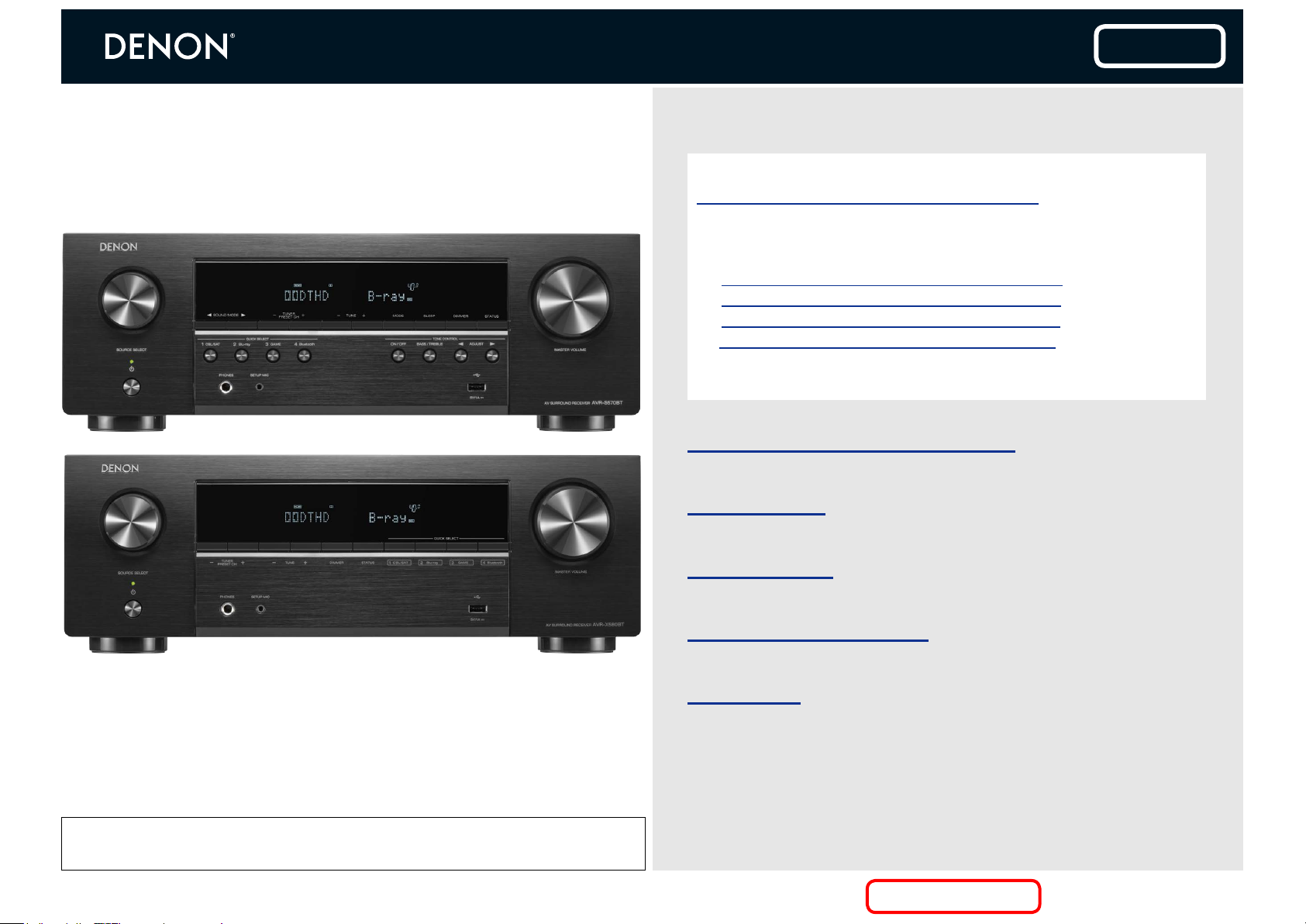
AV SURROUND RECEIVER
Service Manual
Ver. 2
AVR-S570BT
AVR-X580BT
Click here!
On-line service parts list
https://dmedia.soundunited.com/documents/details/29325
ONLINE PARTS LIST (P5)
WEB owner’s manual
NA: https://manuals.denon.com/AVRS570BT/NA/EN/index.php
EU: https://manuals.denon.com/AVRX580BT/EU/EN/index.php
AP: https://manuals.denon.com/AVRX580BT/AP/ZH/index.php
JP: https://manuals.denon.com/AVRX580BT/JP/JA/index.php
Upload is planned for the time of a future press release.
BEFORE SERVICING THIS UNIT
ELECTRICAL
MECHANICAL
This Unit
Before Servicing
Electrical Mechanical Repair Information Updating
•Forpurposesofimprovement,specicationsanddesignaresubjecttochangewithoutnotice.
•Pleaseusethisservicemanualwhenreferringtotheoperatinginstructionswithoutfail.
•Someillustrationsusedinthisservicemanualareslightlydifferentfromtheactualproduct.
REPAIR INFORMATION
UPDATING
Please refer to the MODIFICATION NOTICE.
Condential
Page 2

SAFETY PRECAUTIONS
BEFORE SERVICING THIS UNIT
NOTE FOR SCHEMATIC DIAGRAM
HANDLING THE SEMICONDUCTOR AND OPTICS
ONLINE PARTS LIST
Accessing the Parts List
Searching Part Numbers or Ref. Numbers
NOTE FOR PARTS LIST
SERIAL NUMBER
Serial Number Organization
SKU Code of this Unit
POST-SERVICE PRECAUTIONS
Initializing this Unit AVR-S570BT
Initializing this Unit AVR-X580BT
This Unit
Before Servicing
Electrical Mechanical Repair Information Updating
2
Page 3

SAFETY PRECAUTIONS
The following items should be checked for continued protection of the customer and the service technician.
Leakage current check
Before returning the set to the customer, be sure to carry out either (1) a leakage current check or (2) a line to chassis resistance check. If the leakage current exceeds 0.5 milliamps, or if the resistance from
chassis to either side of the power cord is less than 460 kohms, the set is defective.
Be sure to test for leakage current with the AC plug in both polarities, in addition, when the set's power is in each state (on, off and standby mode), if applicable.
This Unit
CAUTION
Please heed the following cautions and instructions during
servicing and inspection.
◎ Heed the cautions!
Cautions which are delicate in particular for servicing are labeled on the cabinets, the parts and the
chassis, etc. Be sure to heed these cautions and the cautions described in the handling instructions.
◎ Cautions concerning electric shock!
(1) An AC voltage is impressed on this set, so if you touch internal metal parts when the set is energized,
you may get an electric shock. Avoid getting an electric shock, by using an isolating transformer and
wearing gloves when servicing while the set is energized, or by unplugging the power cord when
replacing parts, for example.
(2) There are high voltage parts inside. Handle with extra care when the set is energized.
◎ Caution concerning disassembly and assembly!
Through great care is taken when parts were manufactured from sheet metal, there may be burrs on the
edges of parts. The burrs could cause injury if ngers are moved across them in some rare cases. Wear
gloves to protect your hands.
◎ Use only designated parts!
The set's parts have specic safety properties (re resistance, voltage resistance, etc.). Be sure to use
parts which have the same properties for replacement. The burrs have the same properties. In particular,
for the important safety parts that are indicated by the z mark on schematic diagrams and parts lists,
be sure to use the designated parts.
◎ Be sure to mount parts and arrange the wires as they were originally placed!
For safety seasons, some parts use tapes, tubes or other insulating materials, and some parts are
mounted away from the surface of printed circuit boards. Care should also be taken with the positions
of the wires by arranging them and using clamps to keep them away from heating and high voltage
parts, so be sure to set everything back as it was originally placed.
◎ Make a safety check after servicing!
Check that all screws, parts and wires removed or disconnected when servicing have been put back
in their original positions, check that no serviced parts have deteriorated the area around. Then make
an insulation, check on the external metal connectors and between the blades of the power plug. And
otherwise check that safety is ensured.
(Insulation check procedure)
Unplug the power cord from the power outlet, disconnect the antenna, plugs, etc., and on the power.
Using a 500V insulation resistance tester, check that the insulation resistance value between the inplug
and the externally exposed metal parts (antenna terminal, headphones terminal, input terminal, etc.) is
1M Ω or greater. If it is less, the set must be inspected and repaired.
CAUTION
Many of the electric and the structural parts used in the set have special safety properties. In most
cases these properties are difcult to distinguish by sight, and the use of replacement parts with higher
ratings (rated power and withstand voltage) does not necessarily guarantee that safety performance
will be preserved. Parts with safety properties are indicated as shown below on the wiring diagrams and
the parts list in this service manual. Be sure to replace them with the parts which have the designated
part number.
(1) Schematic diagrams Indicated by the z mark.
(2) Parts lists Indicated by the z mark.
The use of parts other than the designated parts could cause electric shocks, res or other dangerous
situations.
Concerning important safety parts
Before Servicing
Electrical Mechanical Repair Information Updating
3
Page 4
NOTE FOR SCHEMATIC DIAGRAM
WARNING:
Parts indicated by the z mark have critical characteristics. Use ONLY replacement parts recommended
by the manufacturer.
CAUTION:
Before returning the set to the customer, be sure to carry out either (1) a leakage current check or (2)
a line to chassis resistance check. If the leakage current exceeds 0.5 milliamps, or if the resistance from
chassis to either side of the power cord is less than 460 kohms, the set is defective.
WARNING:
DO NOT return the set to the customer unless the problem is identied and remedied.
NOTICE:
(1) ALL RESISTANCE VALUES IN OHM. k=1,000 OHM / M=1,000,000 OHM
(2) ALL CAPACITANCE VALUES ARE EXPRESSED IN MICRO FARAD, UNLESS OTHERWISE INDICATED. P
INDICATES MICRO-MICRO FARAD. N INDICATES NANO FARAD.
(3) EACH VOLTAGE AND CURRENT ARE MEASURED AT NO SIGNAL INPUT CONDITION.
(4) CIRCUIT AND PARTS ARE SUBJECT TO CHANGE WITHOUT PRIOR NOTICE.
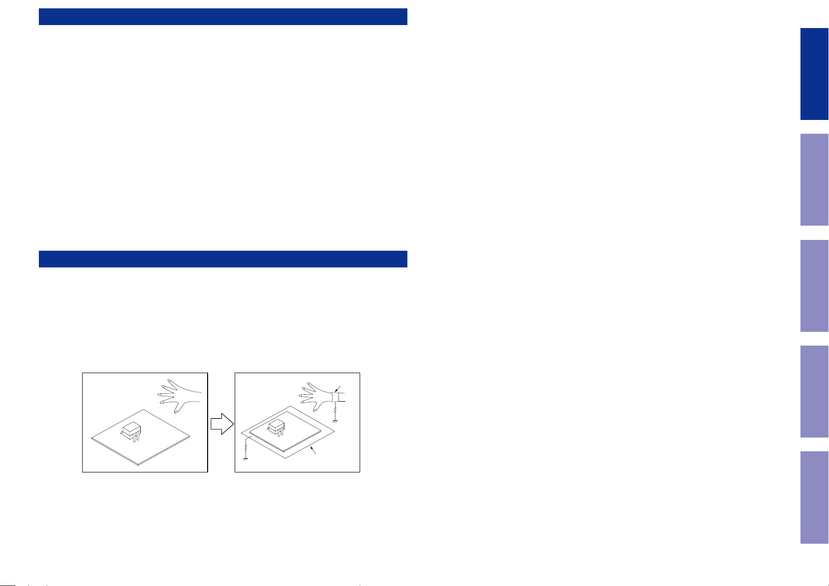
HANDLING THE SEMICONDUCTOR AND OPTICS
Electrostatic breakdown of the semi-conductors or optical pickup may occur due to a potential
difference caused by electrostatic charge during unpacking or repair work.
1. Ground for Human Body
Be sure to wear a grounding band (1 M ohm) that is properly grounded to remove any static electricity
that may be charged on the body.
2. Ground for Workbench
Be sure to place a conductive sheet or copper plate with proper grounding (1 M ohm) on the workbench
or other surface, where the semi-conductors are to be placed. Because the static electricity charge
on clothing will not escape through the body grounding band, be careful to avoid contacting semiconductors with your clothing
<Incorrect>
<Correct>
Grounding Band
This Unit
Before Servicing
Electrical Mechanical Repair Information Updating
PCB
1MΩ
PCB
Conductive Sheet or
Copper Plate
1MΩ
4
Page 5
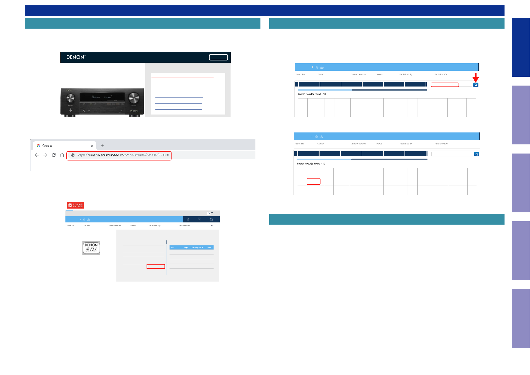
ONLINE PARTS LIST
A
sset No:Owner:Current Version:Status:Published By:Published On
:
k
XXXXXXXXXXXXXXXX
XXXXXXXXXXXXXXXX
32.2Major09-May-2019Vie
w
e
s
ve
Search Result(s) Found - 10
A
sset No:Owner:Current Version:Status:Published By:Published On
:
Search Result(s) Found - 10
A
sset No:Owner:Current Version:Status:Published By:Published On
:
Accessing the Parts List
(1) Access from the Service Manual
・ Click the URL link on the cover of the service manual.
Examples of display
INTEGRATED NETWORK AV RECEIVER
Service Manual
AAA-AAAA
NOTE : If the web browser does not open automatically, copy the URL and paste it into the address bar
of the web browser and then press Enter.
(2) Accessing the Part List from the Model Asset Screen.
・ Display Model Asset from New SDI.
・ Click the section displayed as ▼ Link to Part Lists under the model name.
Click here!
On-line service parts list
AVR-X1700H: https://dmedia.soundunited.com/documents/details/28727
AVR-S760H: https://dmedia.soundunited.com/documents/details/28728
ONLINE PARTS LIST (P5)
WEB owner’s manual
NA: http://manuals.denon.com/AVRX1700H/NA/EN/index.php
EU: http://manuals.denon.com/AVRX1700H/EU/EN/index.php
AP: http://manuals.denon.com/AVRX1700H/AP/ZH/index.php
JP: http://manuals.denon.com/AVRX1700H/JP/JA/index.php
NA: http://manuals.denon.com/AVRS760H/NA/EN/index.php
EU: http://manuals.denon.com/AVRS760H/EU/EN/index.php
Upload is planned for the time of a future press release.
Ver. 1
Searching Part Numbers or Ref. Numbers
You can search a Parts List for part numbers or Ref. numbers.
(1) Enter the part number or Ref. number in the search window of the Parts List, and press the search
button.
(2) The search results are displayed.
The name of the sheet in which the search part is used and the part’s line are displayed.
(3) Next, click the "Sheet" section of the search results.
SR6014 Parts List
21095 Super Administrator 1.2 Published Kazuhiro Nakai 23-Jul-2019
FRONT INPUT VIDEO F.CNT S.CNT DIGITAL
1 SMPS D9001 943203500730S
2 SMPS D9002 943203500730S
SR6014 Parts List
21095 Super Administrator 1.2 Published Kazuhiro Nakai 23-Jul-2019
FRONT INPUT VIDEO F.CNT S.CNT DIGITAL
1 SMPS D9001 9432 03500730S
2 SMPS D9002 9432 03500730S
3 SMPS D9003 9432 03500730S
Download Package
Download Package
(525.24 KB)
(525.24 KB)
Create Public URL
DIODE, RECTIFIER,
AXIAL
DIODE, RECTIFIER,
AXIAL
Create Public URL
DIODE, RECTIFIER,
AXIAL
DIODE, RECTIFIER,
AXIAL
DIODE, RECTIFIER,
AXIAL
943203500730S
CVD1N4007SL 1
CVD1N4007SL 1
943203500730S
CVD1N4007SL 1
CVD1N4007SL 1
CVD1N4007SL 1
This Unit
Before Servicing
Electrical Mechanical Repair Information Updating
All Assets Tasks Drafts Notifications Deactivated Archived Advanced Search
XXXXXXXXXX
0000 XxxxxXxxxx 32.2 Published XxxxxXxxxx 09-May-2019
Download Packag
(392.35 MB)
Additional Classification
Brand
Region
Asset Type SDI
Category
Description ▼Link to Parts List
Denon
AP - JAPAN, NA, E
U, AP - CHINA
Version History
Version No. Type Created On
32.1 Major 23-Apr-2019 View
32.0 Major 07-Feb-2019 View
31.0 Major 07-Feb-2019 View
30.0 Major 24-Dec-2017 View
Search
Edit Thi
DeactivateArchi
Content
Search
Bac
NOTE FOR PARTS LIST
1. Parts indicated by "
nsp
" on this table cannot be supplied.
2. When ordering a part, make a clear distinction between "1" and "I" (i) to avoid mis-supplying.
3. A part ordered without specifying its part number can not be supplied.
4. Part indicated by "@" mark is not illustrated in the exploded and packaging view.
WARNING: Parts indicated by the z mark have critical characteristics. Use ONLY replacement parts
recommended by the manufacturer.
NOTE : If the ▼ Link to Parts List section is not displayed, download the parts table from the Asset list.
5
Page 6
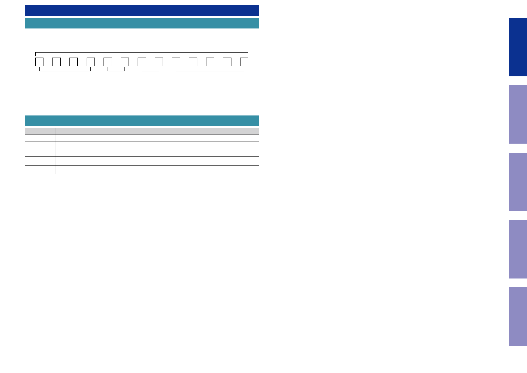
SERIAL NUMBER
Serial Number Organization
The 13-digit serial number that contains the code of the manufacturing date.
13 digits
This Unit
SKU code Month
(01 ~ 12)
The last
2digit of year
Cumulative
serial number
SKU Code of this Unit
SKU Code NAV Number Product Name Description
DBZL 300614-01-00-101 AVRS570BTBKE3 Blk - - Pwr,NA-120V
DBZG 300613-01-00-201 AVRX580BTBKE2 Blk - - EU-Lmtd,220-240V
DBZK 300613-01-00-209 AVRX580BTBKEA Blk - - Australia/New Zealand Only
DBZJ 300613-01-00-206 AVRX580BTBKE1C Blk - - China Only
DBZH 300613-01-00-102 AVRX580BTK Blk - - Pwr,JP-100V
Before Servicing
Electrical Mechanical Repair Information Updating
6
Page 7
POST-SERVICE PRECAUTIONS
Initializing this Unit
Make sure to initialize this unit after replacing the microcomputer or any peripheral equipment, or the
digital PCB.
1. Press the power button to turn off the power.
2. While holding down buttons "
the power button to turn on the power.
3. Release the buttons after conrming that the display ashes at 1-second intervals.
* The unit is initialized.
NOTE: • If the unit fails to enter the service mode in step 3, repeat the procedure from step 1.
• Initializing the device restores the customized settings to the factory settings. Write down
your settings in advance and recongure the settings after initialization.
AVR-S570BT
AVR-S570BT
SOUND MODE
SOUND
X
MODE
1
" and "
1
PRESET CH +
TUNER PRESET CH+
TUNER
" simultaneously, press
Initializing this Unit
Make sure to initialize this unit after replacing the microcomputer or any peripheral equipment, or the
digital PCB.
1. Press the power button to turn off the power.
2. While holding down buttons "
button to turn on the power.
3. Release the buttons after conrming that the display ashes at 1-second intervals.
* The unit is initialized.
NOTE: • If the unit fails to enter the service mode in step 3, repeat the procedure from step 1.
• Initializing the device restores the customized settings to the factory settings. Write down
your settings in advance and recongure the settings after initialization.
AVR-X580BT
AVR-X580BT
TUNER PRESET CH+
TUNER
X
PRESET CH +
TUNE +
" and "
TUNE +
" simultaneously, press the power
This Unit
Before Servicing
Electrical Mechanical Repair Information Updating
7
Page 8

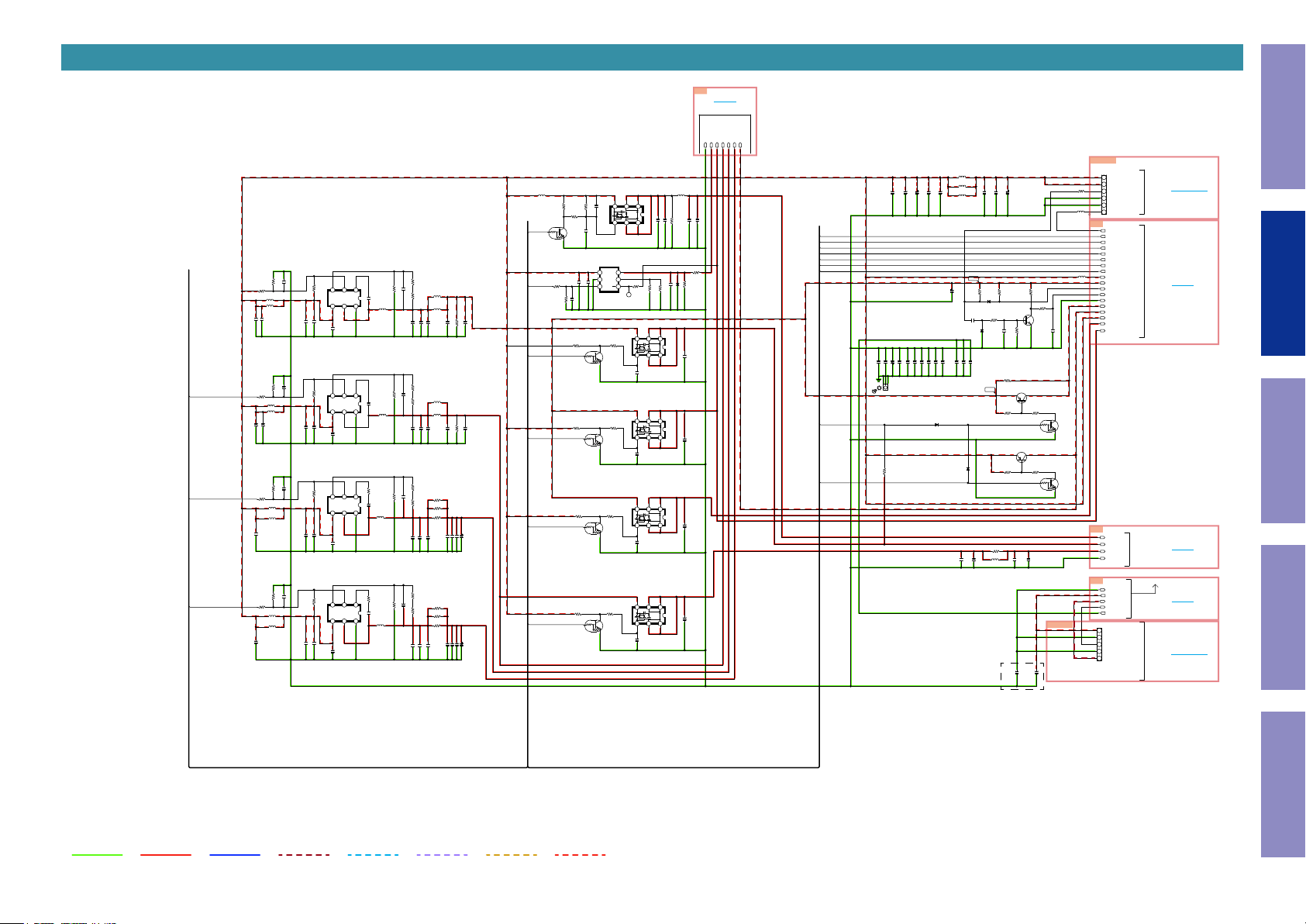
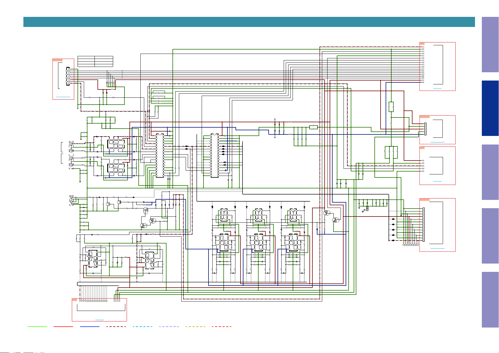
ELECTRICAL
SCHEMATIC DIAGRAMS
SCH01 DIGITAL MCU
SCH02 DIGITAL HDMI TX
SCH03 DIGITAL DSP
SCH04 DIGITAL INPUT VOLUME
SCH05 DIGITAL DIGITAL POWER
SCH06 MAIN AMP
SCH07 USB, BT
SCH08 FRONT
SCH09 REGULATOR
SCH10 SMPS
PRINTED CIRCUIT BOARDS
DIGITAL
MAIN, TUNER, PHONE WIRE GUIDE, FRONT CABLE GUIDE, USB WIRE GUIDE
USB, FRONT, PHONE, STANDBY, MIC
REGULATOR, SMPS
LEVEL DIAGRAM
FRONT ch
CENTER ch
SURROUND ch
SUBWOOFER ch
BLOCK DIAGRAM
ANALOG AUDIO DIAGRAM
DIGITAL AUDIO / HDMI DIAGRAM
VIDEO DIAGRAM
POWER DIAGRAM
WIRING DIAGRAM
SEMICONDUCTORS
1. IC's
2. FL DISPLAY
This Unit
Before Servicing
Electrical Mechanical Repair Information Updating
Remote Code Table
8
Page 9
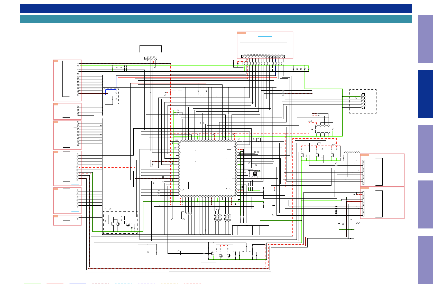
SCHEMATIC DIAGRAMS
SCH01 DIGITAL MCU
A0
A1
A2
A3
A4
A5
MAIN_V OL_M UTE
MAIN_V OL_C LK
MAIN_V OL_D ATA
TO INPU T/VO LUM E PAR T
TO TX P ART
DSP _MOD E_S EL
TO DSP PART
H5V OUT _POW ER
FRO M/T O DIG ITAL POW ER PA RT
HD MI_OS D_S CLK
HD MI_OS D_M OSI
HD MI_OS D_M ISO
TO HD MI TX PAR T
DSP _SPC 1_IRQ
POW ER_D OWN
HD MI_OS D_C S
MCU PART
MCU +3V 3
AGND
SUB _MUT E
DGND
MIC_ SIGNAL
DAC _MU TE
SEL_ CLK
SEL_ DAT A
TUN ER_IN T
TUN ER_R ST
TUN ER_C E
TUN ER_S DIO
TUN ER_
SCL K
+12V
-12V
TO 0A
TX_ TEM P
HSC L
HSD A
TX_ HINT
TX_ HAIN T
TX_ RST
CEC _COM
TO 1A
DIR_ INT
COD EC_M UTE
DIR_ CE
DIR_ RST
DIR_ MOSI
DIR_ CLK
DIR_ MISO
HD MI_SW
DSP _CS
DSP _PCP _BSY
DSP _RST
DSP _MOS I
DSP _MISO
DSP _CLK
TO 2A
MAIN_P OWER
CEC_ POW ER2
CPU _POW ER
CEC_ POW ER
CEC_ POW ER3
DA_ POW ER
USB _POW ER2
MCU +5V
MCU +3V 3
MCU _RST
DGND
SWM 3V3
SWM 5V
D5V
USB 3V3
CEC3 V3
TO 3A
HINS EL_A
HINS EL_B
HINS EL_C
H5V _DE T
HPD 4
HPD 3
HPD 2
HPD 1
TO 4A
FLAS H_O E
AUD IO_O E
TO 5A
DAC_ MUT E
SEL_D ATA
MAIN_VO L_MU TE
MAIN_VO L_CL K
MAIN_VO L_DA TA
TUNER _INT
TUNER _RST
TUNER _CE
TUNER _SD IO
TUNER _SCL K
TX_H INT
TX_H AINT
CODE C_MU TE
DSP_ MOD E_SEL
DIR_R ST
DIR_M OSI
DIR_C LK
DIR_M ISO
HDMI _SW
DSP_ SPC1_IR Q
DSP_ PCP_ BSY
DSP_ RST
DSP_ MOSI
DSP_ MISO
DSP_ CLK
MAIN_PO WER
CPU_P OWE R
CEC_P OWE R
CEC_P OWE R3
DA_P OWE R
B_PO WER2
US
H5VO UT_ POW ER
POWE R_DO WN
HDMI _OSD _SC LK
HDMI _OSD _MO SI
HDMI _OSD _CS
HDMI _OSD _MIS O
HINSE L_A
HINSE L_B
HINSE L_C
H5V_ DET
F
LASH _OE
AUDIO _OE
SEL_C LK
DIR_C E
DSP_ CS
CN711
FOR UPD ATE (MP: OPEN )
7.BOOT
6.N.C
5.D GND
3.TX
4.RX
1.RE SET
2.MC U+3 V3
CN714
7654321
FFC 1mm P ITCH
0.1uF
0.1uF
0.1uF
0.1uF
C7142
C7141
C7120
22K
R7147
22K
22K
R7148
PO WER- FAIL
R7167
Q7109
KTA1504S YRT K
0.1uF
C7121
HSCL
HSDA
R7136 47K
R7137 47K
POWE R_DO WN
USB_ POWE R2
C7115
0.1uF
47K
R7127
CPU_P OWE R
MAIN_PO WER
HINSE L_C
HINSE L_B
HINSE L_A
H5V_ DET
DA_P OWE R
HDMI _OSD _MO SI
HDMI _OSD _MIS O
HDMI _OSD _SC LK
HDMI _OSD _CS
100K
0.1uF
Q7110
C7132
KTC3875S YRT K
33K
R7168
C7133
10V/100uF
T7102
C7114
T7109
0.1uF
R7129 1K
R7131 33
R7132 33
R7133 33
R7134 33
T7104
AUDIO _OE
FLASH _OE
0
R7170
T7108
BOOT M ODE
HIGH :UP DAT E
LOW :NOR MAL
T7125
T7103
R7141 10K
R7138 10K
R7139 100
MCU+3V 3
C7116
0.1uF
T7105
TX_H INT
111
109
110
108107106105104103102101100
DEBU G
DEBU G
TX_H INT
VFD_ DAT A
999897969594939291908988878685848382818079787776757473
THER MALDE T_B
VFD_ CLK
VFD_ CE
PWR_ FAIL_ PROT ECT
VDD_9
VSS_9
VOL_ DOW N
VOL_ UP
CPU_ POW ER
MAIN_PO WER
HINSE L_C
HINSE L_B
HINSE L_A
H5V_ DET
NC
VDD_8
VSS_8
HDM I_TES T_N C
FLASH _OE
AUDI O_OE
CEC_ OUT
USB_ POW ER1
VDD_1
VSS_1
NCNCHPD 4
7271706968
0.1uF
C7113
T7123
T7124
T7106
TX_H AINT
112
TX_H AINT
113
ASO_ DET
R7174 33
R7173 33
HPD3
HPD4
115
116
114
H/P_ RLY
VFD_ RST
USB_ POW ER2
77.DA_ POW ER
76.HDM I_OS D_M OSI
75.HDM I_OS D_M ISO
74.HDM I_OS D_SC LK
73.HDM I_OS D_C S
HPD 3
HPD 2
HPD 1
67
66
65
R7175 33
R7176 33
HPD2
H5VO UT_ POW ER
HPD1
R7140 10K
R7143
0.1uF
C7117
121
119
117
120
118
VDD_10
VSS_10
H/P_ DET
GRN_L ED
WAK E_UP
108.VDD
107.VSS_2
106.PCAP _2
105.DEB UG/JT MS
104.NC
103.THE RMALDE T_A
102.UPD ATE_ RX
101.UPD ATE_ TX
ST M32F101ZG
H5VO UT_ POW ER
VDD_7
HDM I_SW
CEC_ POW ER3
VSS_7
64
63
62
616059
0.1uF
C7112
HDMI _SW
CEC_P OWE R3
CEC_ OUT
CEC_ IN
TX_R ST
DAC_ MUT E
R7142 10K
TUNER _SCL K
33
33
R7144
128
126
124
122
127
125
123
HSD A
HSCL
DAC_ MUT E
REMO TE_IN
TUNE R_SC LK
EEPROM _SCL
EEPROM _SDA
TUNER _CE
TUNER _SD IO
0.1uF
T7126
C7118
134
137
135
133
131
129
138
136
132
130
DEBU G
BOOT0
DEBU G
VDD_11
VSS_11
TX_R ST
CEC_ CTL
SW_M UTE
TUNE R_SD IO
CP_R ESET _NC
1.DC _PRO TECT
2.USB _DA C_M UTE
3.POW ER_ DOW N
4.FRO NT_R LY
5.C/S _RLY
IC711
MC U
33.VDDA
34.AMPSIG_ DET _NC
35.USB_ RST
36.USB_ RX
DIR_C LK
CODE C_M UTE
DIR_M OSI
DIR_M ISO
CURREN T_D ET_N C
DSP_ MOD E_SE L
VSS_6
CEC_ POW ER
DSP_ SPC1_IR Q
DIR_R ST
DSP_ RST
BOOT1
TX_T EMP
DSP_ MOSI
VDD_6
DSP_ PCP_ BSY
DIR_C E
58
57
56
55
54535251504948
47
46
45
44
434241
0.1uF
C7111
1 2 3 4
1 2 3 4
100x4
RN712
5 6 7 8
5 6 7 8
DSP_ PCP_ BSY
DIR_C E
DSP_ SPC1_IR Q
CODE C_MU TE
DIR_R ST
DSP_ MOD E_SEL
DSP_ RST
DIR_M OSI
DIR_C LK
DSP_ MISO
DSP_ MOSI
CEC_P OWE R
10K
R7178
DIR_M ISO
SWM 3V3
OPEN
C7134
4.7K
2.2M
R7180
R7181
Q7112
Q7113
3875SYRT K
100K
R7179
Q7111
KTC2875A S
KTC
KTC3875S YRT K
C7143
R7145
POW ER-FA IL
HSCL
HSDA
TX_R ST
HPD4
HPD3
HPD2
HPD1
R7196
0
2.2K
Q7108
R7166
KTC3875S YRT K
TUNER _INT
TUNER _RST
141
140
139
TUNE R_CE
TUNE R_INT
TUNE R_RS T
MIC_D ET
OSC32_IN
OSC32_O UT
HI-B_ RELY
SEL_C LK
SEL_D ATA
CP_S DA_N C
CEC_ POW ER2
MAIN_VO L_MU TE
MAIN_VO L_D ATA
MAIN_VO L_CL K
XTAL _IN
XTAL _OU T
DSP_ CS
DSP_ MISO
DSP_ CLK
40
DSP_ CLK
DSP_ CS
47K
R7182
27
OPEN
OPEN
OPEN
L7101
C7122
C7123
0.1uF
C7119
470K
R7101
R7102
144
142
143
0
VSS_3
VDD_3
RED_ LED
VBAT
C7101
0.1uF
9 8 7 6 5 4 3 2 1
ISEL_ B
ISEL_ A
VSS_5
C7102
VDD_5
0.1uF
USB_ EN
24 23 22 21 20 19 18 17 16 15 14 13 12 11 10
RESET
KEY1
KEY2
KEY3
OPTIO N
0.1uF
C7105
VSSA
C7106
VREF-
0.1uF
VREF+
34 33 32 31 30 29 28 27 26 25
VDD_4
VSS_4
USB_ TX
36 35
39
38
37
MCU+3V 3
0.1uF
C7110
100x4
R7113
RN711
OPTIO N
*OP TION
S570BT E3
R7113
4K7
R7114
R7184
220K
100K
220P
R7183
C7135
CEC -PAR T
23.CPU _POW ER
25.MCU _3V3
27.NC
24.MCU +5V
26.DGND
24 22
23 21
L7105
L7103
L7106
L7102
L7104
0
FCM601T0 5
FCM601T0 5
FCM601T0 5
MAIN_VO L_CL K
MAIN_VO L_DA TA
MAIN_VO L_MU TE
T7120
R7107
R7108
OPEN
C7108
C7107
R7114
OPTIO N
X580BT E2
X
10K
D7102
KDS160R TKP
R7185
27K
TO BN12B1
TO FRON T B'D
FFC W AFER /27P/1 .25mm
18.RC_ IN
16.RED _LED
17.W/G _LED
19.FL_ RST
20.FL_ CE
21.FL_ CLK
22.FL_ DAT A
14.KEY _2
15.KEY _1
1618
2026
1517
1925
L7114
L7111
L7113
L7115
L7110
L7112
L7108
L7107
L7109
0
0
0
0
0
0
0
0
0
0
R7104
1K
47K
R7103
D7101
OPEN
T7118
T7119
T7101
C7103
33pF
34
1M
8MHz
X7111
1 2
C7104
0
33pF
OPEN
OPEN
C7109
OPEN
R7192
OPEN
R7195
*O PTIO N TAB LE
X580BT E1C
X580BT K
10K
10K
10K10K
X
SWM 5V
1.2K
R7186
3.3K
0.1uF
R7187
C7136
DGND
13.KEY _3
L7116
0
2.ISE L_B
8.MIC _GND
3.MIC _DE T
4.PO WER _KEY
6.-12V
10.H/P _DE T
12.VSE L_B
L7117
0
1.ISE L_A
9.NC
1011121314
L7119
L7120
L7122
L7130
0
0
0
OPEN
C7149
FCM601T0 5
SEL_C LK
SEL_D ATA
R7194
OPEN
R7193
L7123
OPEN
L7124
0
0
L7126
L7125
0
0
R7149 10K
R7150 10K
R7151 10K
R7188 10K
P
FFC 27
123456789
L7127
0
0.1uF
0.1uF
0.1uF
0.1uF
C7124
0.1uF
C7127
C7125
C7126
C7144
CN715
9PIN WAFE R
1
1.MC U+3 V3
2
2.D GND
R7152 1K
3
3.RE SET
4
4.JTD O
5
5.JTC K
6
6.JTM S
7
7.JTD I
8
8.NJT RST
9
9.D GND
USE ONL Y DE BUG
T7110
T7111
T7112
T7113
T7114
T7115
T7116
T7117
CN712
100
OPEN
R7163
C7154
OPEN
C7155
0.1uF
CN712
CA2005-WV 11-K
11
11.TH ERMALD ET_B
10
10.TH ERMALD ET_A
987654321
9.AS O_D ET
8.NC (CURRE NT_D ET)
7.+ /-B D ETEC T
6.D C_PR OT
5.NC (AMPSIG _DE T)
4.C/ S_RL Y
3.FRO NT_ RLY
2.H /P_RL Y
1.H I-B_R LY
CN713
CN713
CA2005-WV 11-K
1.D 5V
2.D 5V
C7153
0.1uF
3.D GND
4.D GND
5.US B3V 3
6.US B_PO WER 1
7.MC S_T X
RX
8.MC S_
9 8 7 6 5 4 3 2 1
9.MC S_RS T
10.USB _DA C_MU TE
11 10
11.USB _EN
C7156
0.1uF
T7131
T7132
C7157
0.1uF
TO MAIN B' D
WA FER/ 9P/2 .0mm
WA FER/ 11P/2.0 mm
FRO M/T O USB /BT B'D
TO BN502
TO BN212
47K
R7156
KTC3875S YRT K
R7153
2.7K
R7154
2.7K
MCU+3V 3
5678
WP
SDA
SCL
VCC
IC712
0.1uF
C7128
1 2 3 4
M24C32WM N6T P
SWM3V3
47K
R7158
TK
Q7105
Q7106
0.01uF
C7129
KTC3875S YR
47K
R7155
GND
A2A1A0
SWM3V3
47K
120K
120K
R7161
R7162
R7159
Q7107
0.01uF
C7146
C7131
0.01uF
C7130
KTC3875S YRT K
R7164 100
R7165 100
C7152
0.1uF
CN711
5.+ 12V
7.MIC _SIGNA L
11.VSE L_A
This Unit
Before Servicing
Electrical Mechanical Repair Information Updating
GND LINE
POWER+ LINE
POWER- LINE
ANALOG AUDIO
DIGITAL AUDIO
TMDS SIGNAL
ANALOG VIDEO
STBY POWER
9
Page 10
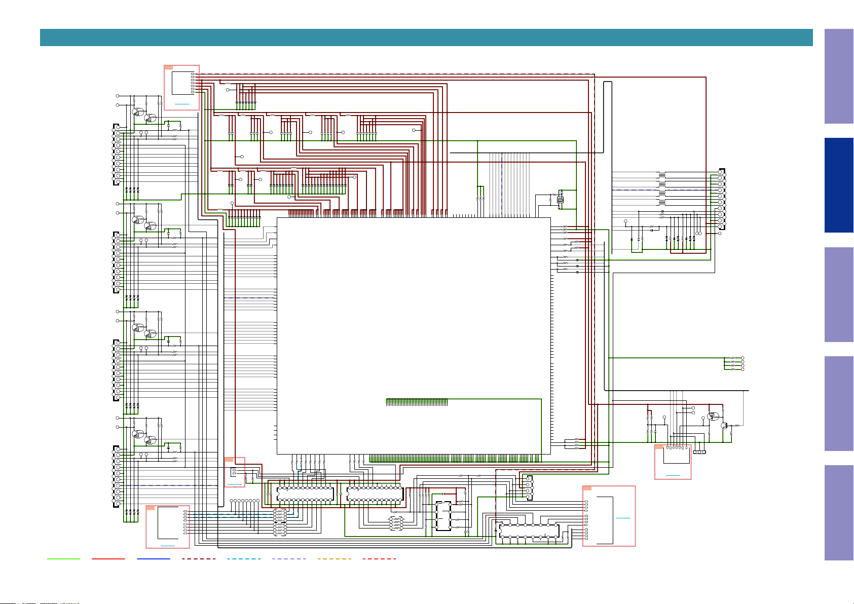
SCH02 DIGITAL HDMI TX
A6
TX PART
+5V_ 4
HPD4
JK794
CJJ9H036Z
19
19.HP DET
18
18.+5 V
17
17.GND
16
16.DDC S DA
5
1
15.DDC C LK
14
14.UT L/HEAC +
13
13.CE R EMOT E
12
12.CK-
11
11.CK SHIE LD
10
10.CK+
9
9.D 0-
8
8.D 0 SH IELD
7
7.D 0+
6
6.D 1-
5
5.D 1 SH IELD
4
4.D 1+
3
3.D 2-
2
2.D 2 SH IELD
1
1.D 2+
H DM I_ INP UT-4 (G ame)
H DM I_ INP UT-3 (B lu -ra y)
H DM I_ INP UT-2 (M e dia P la ye r)
H DM I_ INP UT-1 (C B L/SA T)
19.HP DET
18.+5 V
17.GND
16.DDC S DA
15.DDC C LK
14.UT L/HEAC +
13.CE R EMOT E
12.CK-
11.CK SHIE LD
10.CK+
9.D 0-
8.D 0 SH IELD
7.D 0+
6.D 1-
5.D 1 SH IELD
4.D 1+
3.D 2-
2.D 2 SH IELD
1.D 2+
19.HP DET
18.+5 V
17.GND
16.DDC S DA
15.DDC C LK
14.UT L/HEAC +
13.CE R EMOT E
12.CK-
11.CK SHIE LD
10.CK+
9.D 0-
8.D 0 SH IELD
7.D 0+
6.D 1-
5.D 1 SH IELD
4.D 1+
3.D 2-
2.D 2 SH IELD
1.D 2+
19.HP DET
18.+5 V
17.GND
16.DDC S DA
15.DDC C LK
14.UT L/HEAC +
13.CE R EMOT E
12.CK-
11.CK SHIE LD
10.CK+
9.D 0-
8.D 0 SH IELD
7.D 0+
6.D 1-
5.D 1 SH IELD
4.D 1+
3.D 2-
2.D 2 SH IELD
1.D 2+
+5V_ 3
HPD3
CJJ9H036Z
+5V_ 2
HPD2
CJJ9H036Z
+5V_ 1
HPD1
CJJ9H036Z
OPEN
D7941
JK793
19
18
17
16
15
14
13
12
11
10
9
8
7
6
5
4
3
2
1
OPEN
D7931
JK792
19
18
17
16
15
14
13
12
11
10
9
8
7
6
5
4
3
2
1
OPEN
D7921
JK791
19
18
17
16
15
14
13
12
11
10
9
8
7
6
5
4
3
2
1
OPEN
D7911
1k
R7941
Q7941
KRC102S
DA_4 CK_ 4
OPEN
OPEN
OPEN
D7942
D7943
D7944
1k
R7931
Q7931
KRC102S
DA_3 CK_ 3
OPEN
OPEN
OPEN
D7932
D7933
D7934
1k
R7921
Q7921
KRC102S
DA_2 CK_ 2
OPEN
OPEN
OPEN
D7922
D7923
D7924
1k
R7911
Q7911
KRC102S
DA_1 CK_ 1
OPEN
OPEN
OPEN
D7912
D7913
D7914
CEC 0V9C ORE
TO 6A
10k
R7942
FRO M DIG ITAL POW ER
Q7942
R7943 47K
R7944 47K
KRC102S
0.1uF
C7914
R7946
0
R7947 0
R7948 0
10k
R7932
Q7932
R7933 47K
R7934 47K
KRC102S
0.1uF
C7913
R7936
0
R7937 0
R7938 0
10k
R7922
Q7922
R7924 47K
R7923 47K
KRC102S
0.1uF
C7912
R7926
0
R7927 0
R7928 0
10k
R7912
Q7912
R7914 47K
R7913 47K
KRC102S
0.1uF
C7911
R7916
0
R7917 0
R7918 0
A7
HD MI_MC LK
HD MI_SP DIF
HD MI_SD ATA 0
HD MI_SD ATA 2
HD MI_LR CLK
HD MI_SD ATA 3
TO DSP
HD MI_SD ATA 1
HD MI_B CLK
TO 7A
SWM 5V
CEC 5V
CEC 3V3
CEC 1V8
CEC 0V9
DGND
R7945
R7935
R7925
R7915
L7921
FBMJ3216H L160NT
AVDD33RX
HPD4
L7922
BLM21PG 221SN1
47K
RX0P5 V
RX0SD A
RX0SC L
P0_C-
P0_C+
P0_D0-
P0_D0+
P0_D1-
P0_D1+
L7927
P0_D2-
BLM21PG 221SN1
P0_D2+
L7931
FBMJ3216H L160NT
HPD3
47K
RX1P5 V
RX1SD A
RX1SC L
P1_C-
P1_C+
P1_D0-
P1_D0+
P1_D1-
P1_D1+
P1_D2-
P1_D2+
HPD2
47K
RX2P5 V
RX2SD A
RX2SC L
P2_C-
P2_C+
P2_D0-
P2_D0+
P2_D1-
P2_D1+
P2_D2-
P2_D2+
HPD1
47K
RX3P5 V
RX3SD A
RX3SC L
P3_C-
P3_C+
P3_D0-
P3_D0+
P3_D1-
P3_D1+
P3_D2-
P3_D2+
6.3V/ 10uF
C7921
BLM21PG 221SN1
0.1uF
6.3V/ 10uF
0603
C7928
C7929
AVDD18EA
BLM21PG221S N1
VDD09STB V DD09EA
0.1uF
6.3V/ 10uF
06030603
C7949
C7948
VDD09
0.1uF
0.1uF
0.1uF
0603
6.3V/ 22uF
C7978
C7977
C7976
C7975
RX3P
5V
RX2P5 V
RX1P5 V
RX0P5 V
RX3SC L
RX3SD A
RX2SC L
RX2SD A
RX1SC L
RX1SD A
RX0SC L
RX0SD A
P0_C-
P0_C+
P0_D0-
P0_D0+
P0_D1-
P0_D1+
P0_D2-
P0_D2+
P1_C-
P1_C+
P1_D0-
P1_D0+
P1_D1-
P1_D1+
P1_D2-
P1_D2+
P2_C-
P2_C+
P2_D0-
P2_D0+
P2_D1-
P2_D1+
P2_D2-
P2_D2+
P3_C-
P3_C+
P3_D0-
P3_D0+
P3_D1-
P3_D1+
P3_D2-
P3_D2+
5A
FLASH _OE
AUDIO _OE
FROM MCU
TO A5
HDMI _MCK
HDMI _SPD IF
0.1uF
0.1uF
0.1uF
0.1uF
0603
0603
0603
0603
6.3V/ 10uF
6.3V/ 10uF
C7927
C7926
C7925
C7924
C7923
C7922
0.1uF
6.3V/ 10uF
C7934
C7933
FBMJ3216H L160NT
0.1uF
0.1uF
0.1uF
0603
0603
C7957
C7956
C7955
L7925
FBMJ3216H L160NT
0.1uF
0.1uF
0603
0603
0603
PVDD18VDD18
C7936
C7935
L7930
0.1uF
0.1uF
0.1uF
0.1uF
6.3V/ 10uF
6.3V/ 10uF
6.3V/ 10uF
0603
0603
0603
0603
C7959
C7958
C7964
C7963
C7962
C7961
C7960
L7924
L7923
BLM21PG 221SN1
0.1uF
0.1uF
6.3V/ 22uF
0603
0603
C7930
C7932
C7931
L7929
L7928
FBMJ3216H L160NT
0.1uF
0.1uF
6.3V/ 10uF
6.3V/ 10uF
6.3V/ 10uF
0603
0603
C7951
C7950
C7953
C7952
C7954
AVDD09TX
G14
G13
G12
G11
G10
G16
G7
G15
J7
H7
U13
U14
P17
0.1uF
0.1uF
0.1uF
0.1uF
0.1uF
0.1uF
0.1uF
0603
0603
0603
0603
0603
0603
0603
0603
C7985
C7984
C7983
C7982
C7981
C7980
C7979
HDMI _DA TA0
HDMI _DA TA2
P2
RX3P5V
P1
RX2P5V
N5
RX1P5V
N4
RX0P5V
Y20
RX3SCL
Y19
RX3SDA
E19
RX2SCL
E20
RX2SDA
D20
RX1SCL
D19
RX1SDA
E6
RX0SCL
D4
RX0SDA
A10
P0RX3M
A9
P0RX3P
A8
P0RX0M
A7
P0RX0P
A6
P0RX1M
A5
P0RX1P
A4
P0RX2M
A3
P0RX2P
A21
P1RX3M
A20
P1RX3P
A19
P1RX0M
A18
P1RX0P
A17
P1RX1
A16
P1RX1P
A15
P1RX2M
A14
P1RX2P
K23
P2RX3M
J23
P2RX3P
H23
P2RX0M
G23
P2RX0P
F23
P2RX1M
E23
P2RX1P
D23
P2RX2M
C23
P2RX2P
AA23
P3RX3M
Y23
P3RX3P
W23
P3RX0M
V23
P3RX0P
U23
P3RX1M
T23
P3RX1P
R23
P3RX2M
P23
P3RX2P
D15
CH1SPD IF
D8
CH1BCL K
E9
CH1LRC LK
D9
CH1ASD 0
OPEN
OPEN
R7239
R7238
RCK
HDMI _DA TA3
HDMI _BCK
HDMI _DA TA1
HDMI _L
24 23 22 21 2 0 19 18 17 16 1 5 14 13
0.1uF
0.1uF
VCCB
IC721
VCCA
C7217
C7216
SN74AX C8T245P WR
1234
1234
VDD09_01G8VDD09_02G9VDD09_03
M
OE
VCCB
DIR1A1A2A3A4
56
RN723
78
100x4
56
RN722
100x4
78
R17
09_08
VDD
VDD09_07
VDD09_06
VDD09_05
VDD09_04
VDD09_10
VDD09_09
VDD09_17
VDD09_11H8VDD09_12
VDD09_13
VDD09_16
VDD09_14
VDD09_15
CH0ASD 1
CH0MCL K
CH0SPD IF
CH0BCL K
CH0ASD 0
F19
E16
E15
D16
D17
D18
R7980 33
R7979 33
R7978 33
R7977 33
R7976 33
R7975 33
4
B2B1B3B5B
A5
A6A7A8
54321
L7926
FBMJ3216H L160NT
0.1uF
0.1uF
0.1uF
0.1uF
0.1uF
6.3V/ 10uF
6.3V/ 10uF
0603
0603
C7940
C7939
C7938
C7937
0.1uF
0.1uF
0.1uF
0.1uF
0.1uF
0.1uF
0.1uF
0603
0603
0603
0603
0603
0603
0603
C7970
C7969
C7968
C7967
C7966
C7965
C7971
T7
U7
U8
Y11
Y13
W11
W13
AB8
AB9
AB10
AVDD09EA
VDD09STB_01
VDD09STB_02
AVDD09TX1_02
AVDD09TX0_02
AVDD09TX1_01
AVDD09TX0_01
AVDD09TX1_03
AVDD09TX1_04
AVDD09TX1_05
CH0ASD 3
CH0ASD 2
CH0LRC LK
F20
E18
R7982 33
R7981 33
B7
B6
B8
GND
GND
DIR2
12
1110
9876
0.1uF
6.3V/ 10uF
6.3V/ 10uF
6.3V/ 10uF
AVDD18TX
C7944
C7943
C7942
C7941
AVDD09RX
0.1uF
0.1uF
0.1uF
0603
0603
0603
0603
C7974
C7973
C7972
L19
L20
N19
N20
T22
R22
J22
K22
H22
E13
D13
P22
B14
B15
B16
AB14
AB15
AB16
AVDD09RX2_04
AVDD09RX2_05
AVDD09RX3_01
AVDD09RX3_02
AVDD09RX3_05
AVDD09RX3_04
AVDD09RX2_03
AVDD09RX2_01
AVDD09RX2_02
AVDD09RX1_05
AVDD09RX1_04
AVDD09RX3_03
AVDD09RX1_01
AVDD09RX1_02
AVDD09TX0_03
AVDD09RX1_03
AVDD09TX0_04
AVDD09TX0_05
NCS
SCLK
MISOD7MOSI
E7
E8
D6
33
R7986
R7985 33
R7984 33
R7983 33
24 23 22 21 2 0 19 18 17 16 1 5 14 13
OE
0.1uF
0.1uF
VCCB
VCCB
IC722
A2
VCCA
DIR1
A1
C7215
C7214
SN74AX C8T245P WR
0603
C7945
B8
A1
B2B1B3
A3A4A5
54321
0603
0603
C7947
C7946
E11
D11
B9
B10
AVDD09RX0_05
AVDD09RX0_04
AVDD09RX0_01
AVDD09RX0_02
AVDD09RX0_03
VSS_03
VSS_01A2VSS_02
VSS_04
VSS_05B2VSS_06
B1
A22
A23
AVDD18RX
0603
P
ARCIN
EARCP
EARCM
P1TX 0P
P1TX 3
P1TX 1P
TX1S CL
P1TX 2P
P1TX 0M
TX1S DA
P1TX 1M
P1TX 2M
P1TX 3M
TX1H PD
P1TX 2P
P1TX 2M
P1TX 1P
P1TX 1M
TX_H AINT .
TX_H INT
TX_R ST
HSCL
HSDA
4A
FRO M CP U
HD MI_OS D_S CLK
HD MI_OS D_M OSI
HD MI_OS D_C S
HD MI_OS D_M ISO
HIN SEL_A
HIN SEL_B
HIN SEL_C
H5V _DE T
HPD 4
HPD 3
HPD 2
HPD 1
P1TX 0P
P1TX 0M
P1TX 3P
P1TX 3M
EARCP
TX1S CL
TX1S DA
TX1H PD
EARCM
ARCIN
TO A4
C7992
R7991
10pF
1k
1M
R7992
X7201
R7962 10k
R7963 10k
L17
N17
L5
M17
L7
H5
J5
N7
Y9
K5
K7
H19
M7
W9
18IO_04
VDD18_03
VDD18_07
VDD18_05
VDD18_02
VDD18_06
VDD18_01
VDD18_04
PVDD18PCR
VDD
VDD18IO_01
VDD18IO_02
VDD18IO_03
AVDD18EA_02
AVDD18EA_01
L23
N23
M23
M22
C22
U15
J19
AB12
AC11
PVDD18_1
PVDD18_2
AVDD18TX1_01
AVDD18TX1_02
A11
A13
AA22
B3
B12
B21
AC12
AC13
AVDD18RX2
AVDD18RX3
AVDD18RX0
AVDD18RX1
DD18TX0_02
AVDD33RX2_01
AVDD33RX3_02
AVDD33RX3_01
AVDD33RX2_02
AVDD33RX1_01
AVDD33RX1_02
AVDD18TX0_01
AV
R7961 10k
T4
W4
A12
AVDD33RX0_01
V5
AC14
AC15
AC16
AC17
AC18
AC19
AC20
AC21
P0TX1P
P0TX2P
P0TX1M
P0TX2M
AVDD33RX0_02
AC8
AC9
AC10
TX0SCL
P0TX3P
P0TX0P
P1TX2P
TX0SDA
P0TX3M
P0TX0M
P1TX2M
TX0HP D
Y1
T1
U2
W5
Y7
AA1
Y4
AC3
AC4
AC5
AC6
AC7
P1TX1P
P1TX1M
ARCIN
EARCP
EARCM
XO_NC
TX1SCL
P1TX3P
P1TX0P
TX1SDA
P1TX3M
P1TX0M
TX1HP D
IC791
MN 864807A
L15
N15
L14
N14
L13
N11
N12
N13
L11
L12
L10
N9
K9
J10
J11
J13
J14
NC_01
NC_02
NC_03
NC_04
VSS_13
VSS_14
VSS_15
VSS_12
VSS_11
VSS_07
VSS_08
VSS_09
VSS_10
J9
E12
B11
B13
B23
B22
G17
H17
H20
D12
B5B4B7
B6
A6A7A8
9876
R7236
7 8
5 6
N10
K10
K11
K12
K13
K14
K15
L9
M14
M13
M11
M12
M10
P10
P11
P12
P13
P14
P15
P9
R11
R13
R14
R10
NC_18
NC_30
NC_17
NC_29
NC_16
NC_15
NC_26
NC_27
NC_28
NC_13
NC_14
NC_25
NC_23
NC_12
NC_24
NC_05
NC_06
NC_07
NC_08
NC_09
NC_10
NC_11
NC_22
NC_21
NC_19
NC_20
NC_32
NC_34
NC_35
NC_36
NC_37
NC_39
NC_41
NC_31
NC_33
NC_38
NC_40
VSSRX1_05
VSS_20
VSS_25
VSS_23
VSS_24
VSS_22
VSS_16
VSS_18
VSS_32U5VSS_33
VSS_34
VSS_35
VSS_37
VSS_17
VSS_19
VSS_36
VSS_21
VSS_38
VSS_30
VSS_39
VSS_26
VSS_28R9VSS_29
VSS_31
VSS_27
17
P7
R1
V1
R7
U4
U9
M9
J12
J15
J20
B8
DIR2
1110
W8
L22
R15
R12
N22
U
U10
U11
U12
M19
M20
M15
GND
GND
12
R7233 0
R7232 10k
R7234 33
R7231 10k
R7235 10k
33
1 2 3 4
RN721
100x4
R7230
VSS_42
VSS_43
VSS_44
VSS_40
VSS_45
VSS_41
Y8
Y12
AB1
AB2
W12
C7213
MX25L3233FM 2I-08G
4 3 2 1
OPEN
VSSIO_06N2VSSIO_07
AVSSTX1_02
VSSIO_04
VSSIO_02
VSSIO_03
VSSIO_05
AVSSTX0_02
VSSIO_01
AVSSTX0_01
VSS_52
VSS_53
VSS_46
VSS_47
VSS_48
VSS_49
VSS_50
VSS_51
F5
E5
N1
D5
M4
M5
Y14
AC1
AC2
W14
AC22
AC23
AB11
AB13
AB22
AB23
R7229 33
0.1uF
10k
R7228
R7227
IC725
10k
8765
CS
VCC
R7226
10k
SO
HOL D
R7225
WP
SCLK
0
R7224
VSS
SI
0
OPEN
C7212
AVSSTX0_03
AB17
AB18
AVSSTX0_04
AVSSTX0_05
AVSSTX0_06
AB19
AB20
R7237 33
R7223
AVSSRX0_06
AVSSRX0_05
AVSSTX1_01
AVSSTX1_03
AVSSTX1_04
AVSSRX0_01
AVSSTX1_05
AVSSRX0_02
AVSSRX0_03
AVSSTX1_06
AVSSRX0_04
AVSSTX1_07
AVSSTX0_07
B4
B5
B6
B7
E10
Y10
AB3
AB4
AB5
AB6
AB7
D10
W10
AB21
C7211
OPEN
VSSRX3_06
AVSSRX2_05
AVSSEA_02
AVSSRX2_06
AVSSEA_01
AVSSRX3_05
AVSSRX3_01
AVSSRX3_02
AVSSRX3_03
AVSSRX2_01
AVSSRX2_04
AVSSRX1_06
AVSSRX3_04
AVSSRX2_02
A
A
AVSSRX2_03
AVSSRX1_01
AVSSRX1_02
AVSSRX1_03
AVSSRX1_04
Y2
F22
P19
E22
P20
E14
K19
K20
Y22
V22
B17
B18
B19
B20
AA2
U22
G22
D22
D14
W22
1
2
3
4
5
6
7
16 1 5 14 1 3 12 11 10
B6
B7
B5
VCC
IC723
0.1uF
CVIS N74CBT 3251PWR
B3
B4
B1
ANCOE
B2
PVSS_1
PVSSPCR
J17
U16
SCK
GND
MOS I
VCC
/CS
MISO
GND
B8
25.0MHz
C7993
12pF
U1
XI_SYSC LK
R7964 47K
P5
CEC
R7965 47K
T5
PTEST
R7966 47K
P4
NTEST
R7967 4 k7
G19
NOSDIRQ
R7968 1k
R7969 10
E17
NIRQA
R7970 4 k7
R7971 10
T2
NIRQ
R7972 1k
R4
NRESET
C7994
1000pF
R7973 47
R2
HSCL
C7995
OPEN
R7974 47
R5
HSDA
C7996
OPEN
C2
PCLKOU T
D2
HSYNCO UT
G5
VSYNCO UT
C1
DEOUT
D1
Q23
E4
Q22
E2
Q21
E1
Q20
F1
Q19
F4
Q18
G4
Q17
F2
Q16
G2
Q15
G1
Q14
H4
Q13
H2
Q12
H1
Q11
J2
Q10
J4
Q9
J1
Q8
K2
Q7
K4
Q6
K1
Q5
L4
Q4
L2
Q3
M2
Q2
L1
Q1
M1
Q0
G20
PCLKIN
R19
HSYNCI N
T20
VSYNCIN
R20
DEIN
U20
D23
T19
D22
T17
D21
U19
D20
V20
D19
W20
D18
V19
D17
W19
D16
W17
D15
Y17
D14
W18
D13
W16
D12
Y18
D11
Y16
D10
W15
D9
Y15
D8
W6
D7
W7
D6
Y5
D5
Y6
D4
V4
D3
R7987 OP EN
W2
D2
R7988 47K
V2
D1_LPSA1
R7989 47K
W1
D0_LPSA0
R7990 OP EN
PVSS_2
K17
CN721
CJP07GA 333ZR
MP :O PEN
1.00mm FFC
9
S1
S0
S2
HPD4
HPD3
0
2
HPD
GND
R7222
HPD1
87654321
OPEN
R7211
L7951
4ohm /0605
EXCX 4CZ040X
L7952
4ohm /0605
EXCX 4CZ040X
L7953
4ohm /0605
EXCX 4CZ040X
L7954
4ohm /0605
EXCX 4CZ040X
C7915
1uF
R7951 0
R7952 0
H1_HP
R7953 1 k2
C7916
1uF
1k8
OPEN
OPEN
OPEN
1uF
OPEN
D7951
R7954 47K
C7917
OPEN
R7956 1k 8
R7955
D7952
D7955
D7953
D7954
HSCL
HSDA
TX_R ST
TX_H INT
TX_T EMP
TH791
(OVER 88'C)
NTC T HER MISTO R 10K
0.1uF
R7905 10k
R7906 OPENR7907 OPEN
R7908
1A
HSC L
HSD A
TX_ RST
TX_ HINT
TX_ TEM P
CEC _COM
TX_ HAIN T
FRO M CP U
TO A1
OPEN
OPEN
H1_CK
H1_DA
D7957
D7956
TX_R ST
TX_H INT
TX_H AINT
R7904
321
BN791
PIN HE ADE R (2. 0mm Pit ch)
MP:O PEN
KRA102S
JK795
CJJ9H036Z
1
1.TX 2+
2
2.TX 2 SH IELD
3
3.TX 2-
4
4.TX 1+
5
5.TX 1 SH IELD
6
6.TX 1-
7
7.TX 0+
8
8.TX 0 SH IELD
9
9.TX 0-
10
10.TX C+
11
11.TX C SH IELD
12
12.TX C-
13
13.CE R EMO TE
14
14.UT L/HEAC +
15
15.DDC S CK
16
16.DDC S DA
17.GND
18.+5 V
19.HP DET
H DM I_ OU TPU T
17
18
19
H1_5V
FRO M HD MI 4 K PA RT
R7996 0
HS1
R7997 0
HS2
R7998 0
HS3
R7999 0
HS4
10k
R7903
Q7902
2SC4617EB TLR
TX_H AINT .
R7902
47K
47K
R7901
Q7901
10k
This Unit
Before Servicing
Electrical Mechanical Repair Information Updating
GND LINE
POWER+ LINE
POWER- LINE
ANALOG AUDIO
DIGITAL AUDIO
TMDS SIGNAL
ANALOG VIDEO
STBY POWER
10
Page 11
SCH03 DIGITAL DSP
D SP PART
CJSJSR 1124
OP T2
CB L/SA T
(E3 Ver . AUX )
CJSJSR 1124
OP T1
TV
CB L/SA T
COAX IAL
OP TION
JK784
C7841
R7841
2A
DIR_ INT
COD EC_M UTE
DSP _MOD E_S EL
DIR_ CE
DIR_ RST
DIR_ MOSI
DIR_ CLK
DIR_ MISO
HD MI_SW
DSP _CS
DSP _SPC 1_IRQ
DSP _PCP _BSY
DSP _RST
DSP _MOS I
DSP _MISO
DSP _CLK
50
VSS
VDD
494847
DQ15
DQ0
VSSQ
DQ2
DQ3
VDDQ
DQ4
DQ5
VSSQ
DQ6
DQ7
VDDQ
_CAS
_RAS
_CS
BA
A10/AP
A0
A1
A2
A3
VDD
RN751
1234
DQ14
VSSQ
464544434241403938373635343332313029282726
DQ13
DQ12
VDDQ
DQ11
DQ10
VSSQ
DQ9
DQ8
VDDQ
NC
UDQM
CLK
CKE
NC
A9
A8
A7
A6
A5
A4
VSS
5678
33x4
C7436
+3V3D
0.1uF
RN750
1234
5678
33x4
C7435
0.1uF
C7434
15P
R7430
AD9
AD8
AD7
AD6
AD5
AD4
TO A2
FRO M/T O MCU PAR T
DA7
DA6
DA5
DA4
DA3
DA2
DA1
DA0
SD3
SD6
SD7
75
This Unit
Before Servicing
Electrical Mechanical Repair Information Updating
AD[ 0:19]
DA_ GND1
D_S R-
DGND
+5V A
AGND
DSP _AUD IO
100
0.1uF
1011121314151 6
INT
RESET
AD0/CS
SCL/CCLK
AD1/CD IN
SDA/CDO UT
14.AINR+
16.AINL-
15.AINL+
IC744
CS 42528-CQ
DIR + CO DEC
33.AOUTA2 -
34.AOUTB1 -
35.AOUTB1 +
AGND
VARX
AOUTA1+
AOUTA1-
MUTEC
LPFLT
0.1uF
C7460
R7412
1.37K/F
1000P
C7456
0.022uF
C7457
C7459
0.1uF
C7458
10V/100uF
A9
TO DIGIT AL P OWE R PAR T
R7479
OPEN
* Cirru s Rec ommend
+5VD
OPEN
C7446
0.1uF
C7447
C7728
LRCK1
SCLK1
123456789
64
CX_SDIN 2
VD
VLC
CX_SDIN 3
63
DGND
CX_SDIN 4
62
SAI_SCLK
61
SAI_LRCK
60
2.CX_SCL K
3.CX_LRC K
1.CX_SD IN1
OMCK
59
ADCIN1
58
ADCIN2
57
CX_SDOU T
56
RMCK
55
SAI_SDOU T
54
VLS
53
48.RXP1/GP O1
47.RXP2/GP O2
46.RXP3/GP O3
DGND
52
VD
51
TXP
50
RXP0
RXP7/GPO 7
RXP6/GPO 6
RXP5/GPO 5
RXP4/GPO 4
49
0.01uF
0.01uF
0.1uF
0.1uF
0.1uF
0.01uF
C7464
C7466
C7465
C7463
C7462
C7461
TO 9A
DGND
+1V 8H
+3V 3D
+5V D
L7401
C7442
CB05YT YH221
10V/220uF
C7443
0.1uF
C7444
0.1uF
C7445
16V/100uF
10V/100uF
SCLK2
R7476 100
LRCK2
R7475 3 3
R7474 1K
R7473 1K
SDTO1
MCKO
R7472 220
SDTO2
R7471 33
C7471
0.1uF
C7469
0.1uF
+5VD
C7468
16V/100uF
0.01uF
C7467
Pattern
R7482 OP EN
Pattern
R7483 OPE N
C7475
OPEN
C7476
OPEN
C7480
OPEN
L : A OUT (HD MI off)
H : B OUT ( H DMI o n)
8 7 6 5 4 3 2 1
2Y
GND
3A4Y4B
3Y
3B
9
R7449
C7470
16V/100uF
100
*HD MI SP DIF M ODE : DIR MASTE R
*HD MI I2 S MO DE : H DM I MASTER
*AD C MO DE : DSP MASTER
*DIR MOD E : D IR MAST ER
1A1B1Y2A2B
SEL
4A
VCC
ST
IC745
16151413121110
C7437
0.1uF
* Ci rrus Re commen d
R7424, R7425: 10K -->3. 3K C hang e.
+3V3D
10K
10K
3.3K
R7427
R7428
R7426
4321
DO
WP#
CS#
0.1uF
C7428
CLKNCVCC
8 7 6 5
10K
R7429
+3V3D
R7401
3.3K
RN741
10Kx4
5 6 7 8
RN742
10Kx4
4
X741
R7403
1
2 3
24.576MHz
10pF
C7403
C7404
5 6 7 8
L7402
CB05YT YH221
1M
R7402 330
10pF
1uF
0.01uF
C7406
C7407
C7405
10V/220uF
+3V3D
3.3K
R7425
VSS
IC742
DI
+1V8
MX25L8006EM 2I-12G
C7427
OPEN
1 2 3 4
+3V3D
C7401
0.1uF
C7402
0.1uF
1 2 3 4
R7404
5.1K/ F
C7408
0.1uF
C7409
0.1uF
R7405
3.3K
R7406
+3V3D
3.3K
R7407
10K
R7408
10K
*HD MI AU DIO Count erm easu re
R7447
100
68
68
68
SN74AH C157PW R
R7448
0
68
R7445 0
R7446 0
R7431
R7432
R7444
R7443
R7484
0
(1) SPDIF input
CH1:RXIN0
7A
HDM I_BC LK
HDM I_MCL K
HDM I_SPD IF
HDM I_LRC LK
HDM I_SD ATA0
HDM I_SD ATA1
HDM I_SD ATA2
HDM I_SD ATA3
FROM HD MI_T X
TO A7
100
R7420
SD[ 0:7]
100P
C7425
SD5
SD0
SD1
SD2
AD0
AD1
114
EXT_A17
GNDIO1
5354555657
100
R7416
AD13
5 6 7 8
5 6 7 8
33x4
RN747
1 2 3 4
C7422
110
111
112
113
VDD5
SD_CS#
EXT_A15
EXT_A16
102.SD_A0,E XT_ A0
101.SD_A1,E XT_ A1
100.VDDIO5
99.SD_A2,E XT_ A2
68.SD_D0,E XT_ D0
67.GNDIO2
66.EXT_WE #
65SD_D1,E XT_ D1
DAO1_LRCL K
GND2
VDD2
SD_DQM 0
0.1uF
C7414
10K
10K
R7415
33x4
RN746
1 2 3 4
106
SD_BA1, EXT_ A14
SD_A11,EX T_A1 1
SD_A12,EX T_A1 2
SD_D10,EX T_D 10
SD_D11,EX T_D 11
SD_D12,EX T_D 12
SD_D13,EX T_D 13
SD_D14,EX T_D 14
SD_D15,EX T_D 15
SD_D4,E XT_ D4
616263
+3V3D
103
105
104
GNDIO5
100 101 102
SD_BA0, EXT_ A13
SD_A10,EX T_A1 0
C7420
GNDD4
0.1uF
SD_A3,EX T_A 3
SD_A4,EX T_A 4
C7419
VDD4
0.1uF
EXT_CS2 #
SD_A5,EX T_A 5
GNDIO4
SD_A6,EX T_A 6
SD_A7,EX T_A 7
C7418
VDDIO4
0.1uF
SD_A8,EX T_A 8
SD_A9,EX T_A 9
GND3
0.1uF
C7417
VDD3
R7419
SD_CLKE N
SD_CLKIN
SD_CLKO UT
R7418
SD_DQM 1
SD_D8,E XT_ D8
SD_D9,E XT_ D9
GNDIO3
C7416
VDDIO3
0.1uF
65 66 67 68 69 70 71 72 73 74 75 76 77 78 79 80 81 82 83 84 8 5 86 87 88 89 90 91 92 93 94 95 96 97 98 99
SD_D3,E XT_ D3
VDDIO2
SD_D2,E XT_ D2
64
C7415
0.1uF
+3V3D
0.1uF
107
109
108
SD_RAS#
SD_CAS#
SD_WE#
SD_D5,E XT_ D5
SD_D6,E XT_ D6
SD_D7,E XT_ D7
59
60
58
33
DA12
DA11
DA10 AD12
DA14
DA13
DA15
3.3K
3.3K
3.3K
R7423
R7424
R7422
+3V3D
0.1uF
C7423
C7424
0.1uF
123
122
124
121
GNDIO6
RESET#
SCP1_MOSI
SCP1_MISO/ SDA
1.SCP2_CK
2.SCP2_MISO
3.SCP2_MOS I
4.SCP1_IRQ
CS 497024CVZ
35.DAO2_D3
36.DBDA
37.DBCK
38.DAO2_D2
DAO2_D0,H S3
DAO2_SCLK
GNDD1
DAO2_LRCL K
4647484950
44
45
0.1uF
5 6 7 8
RN743
1 2 3 4
R7411 OPE N
R7409 OPE N
R7410 OPE N
116
118
120
117
119
VDDIO6
EXT_OE#
EXT_A19
EXT_A18
EXT_CS1 #
IC741
AU DIO D SP
DAO1_DAT A1,H S1
DAO1_DAT A0,H S0
DAO1_D2,H S2
DAO1_D3
VDDIO1
51
0.1uF
C7412
33x4
R7413
16V/100uF
115
GND5
DAO1_SCLK
2
5
R7414
128
123456789
PCP/SCP2_I RQ#
SCP1_CS#
PCP/SCP2_C S#
VDDIO7
GNDIO7
GPIO3,DDAC
1011121314151617181920212223242526272829303132333435363738
GPIO2,UAR T_T XD
VDD7
GPIO1,UAR T_RX D
GPIO1,UAR T_C LK,EE_ CS#
GND7
XTAL_OU T
XTI
XTO
GNDA
PLL_REF_RES
VDDA(3.3V)
VDD8
DAI1_DATA 3,D SD3
DAI1_DATA 2,D SD2
GND8
DAI1_DATA 1,D SD1
DAI1_DATA 0,D SD0
VDDIO8
DAI1_BCLK ,DSD -CLK
DAI1_LRCK, DSD 4
GNDIO8
DAI2_LRCK
DAI2_SCLK
DAI2_DATA ,DSD 5
39
C7426
125
127
126
VDD6
GNDD6
SCP1_CLK
SCP1/PCP _BS Y
DAO2_D1,H S4
VDD1
TEST
DAO_MCL K
414243
40
C7410
(3) DAC input
CH1:LRCK
CH2:BCK
CH3:DIN1
AD[ 0:19]
IC743
C7429
M12L16161A5T G2R
10V/100uF
512K * 16B it * 2 Ban ks
SD7
SD6 S D4
SD3
SD4
+3V3D
C7430
RN748
0.1uF
1234
5
DQ1
678
33x4
C7431
0.1uF
RN749
1234
9 8 7 6 5 4 3 2 1
5
678
33x4
LDQM
SD2
SD1
SD0
SD5
C7432
0.1uF
_WE
25 2 4 23 2 2 21 20 19 18 1 7 16 15 14 13 1 2 11 1 0
C7433
0.1uF
AD2
AD3
AD13
AD12
AD0
AD1
RN745
AD2
AD3
DA8
AD4
DA9
AD5
1 2 3 4
5 6 7 8
33x4
RN744
5 6 7 8
33x4
DA10
DA11
AD6
AD7
AD8
DA12
AD9
1 2 3 4
DA13
DA14
DA15
33
33
DA0
DA1
DA2
DA3
DA4
DA5
DA6
DA7
DA8
DA9
R7417
33
DA[ 0:15]
(2) DIR output
CH1:FSDIR1
CH2:64FSDIR1
CH3:DATADIR1
CH4:MCLK
A8
TO 8A
FRO M/TO INPU T/V OLUM E PAR T
CTD_
D_F R-
D_F L-
D_F L+
D_F R+
AD_ RIN-
D_C T+
D_S W+
D_S L-
D_S L+
D_S R+
D_S W-
AD_ LIN+
AD_ RIN+
100
R7477
R7478
C7450
C7452
D_SB RD_SB R+
D_SB L+
D_SB L-
OPEN
0.1uF
0.1uF
L7403
C7453
50V/100uF
+5VD
C7454
C7455
35V/470uF
FCM601T0 5
100P
C7449
C7448
C7451
50V/22uF
VQ
17
AINR-
FILT+
18
REFGND
19
AOUTB4-
20
AOUTB4+
21
AOUTA4+
22
AOUTA4-
23
VA
24
AGND
25
AOUTB3-
26
AOUTB3+
27
AOUTA3+
28
AOUTA3-
29
B2-
AOUT
30
AOUTB2+
31
AOUTA2+
32
33 34 35 36 37 38 3 9 40 41 4 2 43 4 4 45 46 47 48
0.1uF
C7727
0.01uF
L7404
+5VD
AGND
AD_R INAD_R IN+
AD_L IN+
AD_L IN-
D_SR D_SR +
D_SL +
D_SL D_SW D_SW +
D_CT +
D_CT D_FR D_FR +
D_FL +
D_FL +5VA
C7477
C7478
C7479
C7473
0.1uF
C7474
OPEN
T7401
T7402
T7403
T7404
*SOUN D QU ALIT Y Cout erme asu re.
*EMI Cout erm easu re.
R7480
OPEN
R7481
OPEN
AD_ LIN-
0.1uF
0.1uF
0.1uF
JK782
C7822
VCC
RX
0.1uF
GND
R7821 33
1 2 3
OUT
C7824
OPEN
JK783
VCC
C7832
RX
0.1uF
GND
1 2 3
OUT
JK784
C7841
S570BT /E3
O
100pF
O
R7833 33
100P
R7841
X580BT /ALL
R7824 33
R7834 33
33P
C7823
33P
C7833
75
OPEN
D7841
X
0.1u F
X
GND LINE
POWER+ LINE
POWER- LINE
ANALOG AUDIO
DIGITAL AUDIO
TMDS SIGNAL
ANALOG VIDEO
STBY POWER
11
Page 12
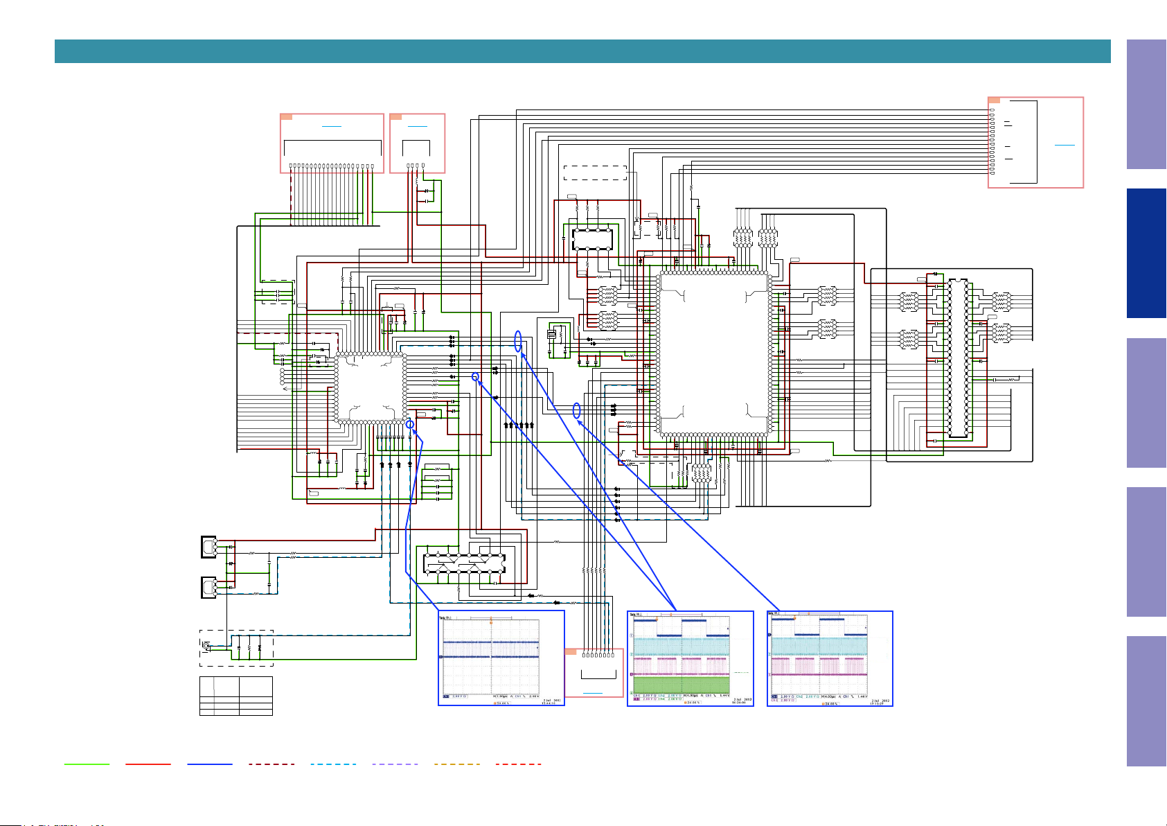
SCH04 DIGITAL INPUT VOLUME
D IGIT AL PO W ER PART
100K
C7511
R7512
0.1uF
CEC_P OWE R3
CEC_P OWE R
CEC_P OWE R
R7511
0.1uF
C7512
R7521
0.1uF
C7525
R7531
0.1uF
C7538
R7541
0.1uF
C7552
33
L7511
CB03YT YH600
L7512
OPEN
10uF
C7513
33
L7521
CB03YT YH600
L7522
OPEN
10uF
C7526
33
L7531
CB03YT YH600
L7532
OPEN
33
L7541
CB03YT YH600
L7542
OPEN
R7522
R7532
R7542
OPEN
R7513
C7515 16V/10uF
C7514 16V/10uF
100K
0.1uF
C7524
OPEN
R7523
C7527 16V/ 10uF
C7528 16V/ 10uF
100k
0.1uF
C7537
OPEN
R7533
C7539 16V/10uF
C7540 16V/10uF
100k
0.1uF
C7551
OPEN
R7543
C7553 16V/10uF
C7554 16V/10uF
VFB
EN
IC751
TPS563201DDC R
3 2 1
VIN
SW
0.1uF
C7516
VFB
EN
IC752
TPS563201DDC R
3 2 1
SW
VIN
0.1uF
C7529
VFB
EN
IC753
TPS563201DDC R
3 2 1
SW
VIN
0.1uF
C7541
VFB
EN
IC754
TPS563201DDC R
3 2 1
SW
VIN
0.1uF
C7556
6A
TO A6
TO HD MI TX PAR T
DGND
CEC 0V9C ORE
CEC 3V3
CEC 0V9
CEC 5V
SWM 5V
CEC 1V8
CN751
CN751
C7592
SWM 3.3V
CN752
CA2505-WV 06L
1.D 5.2V
2 1
2.D 5.2V
R7589
3
3.M_ RESE T
0
4.D _GND
5.D _GND
L7584
6 5 4
6.MAIN_ POW ER
CB03YT YH600
3A
MAIN_P OWER
CEC_ POW ER2
CPU _POW ER
CEC_ POW ER
CEC_ POW ER3
DA_ POW ER
USB _POW ER2
H5V OUT _POW ER
L7585
MCU +5V
CB03YT YH600
MCU +3V 3
POW ER_D OWN
MCU _RST
DGND
SWM 3V3
SWM 5V
D5V
USB 3V3
0.1uF
CEC3 V3
FRO M/T O SMP S B'D
FRO M/T O MCU PAR T
TO BN601
WA FER/ 6P/2 .5mm
TO A3
SWM 5V
9A
+5V D
B0
CN752
CA2005-WV 05-K
5 4 3 2 1
+3V 3D
+1V 8H
DGND
DA_ GND2
+5V A
USB /BT_ L
USB /BT_ R
AGND
1.+ 5VA
2.D A_GND
3.US B/BT _R
4.D A_GND
5.US B/BT _L
TO A9
TO DSP PART
FRO M/T O INP UT/V OLUM E PA RT
TO 0B
TO BN211
TO USB /BT B'D
WA FER/ 5P/2 .0mm
L7581
CB03YT YH600
L7582
CB03YT YH600
0.1uF
0.1uF
OPEN
0.1uF
C7597
L7583
0.1uF
OPEN
C7584
C7585
C7586
CB03YT YH600
16V/470uF
OPEN
C7158
1uF
1uF
0.1uF
0.01uF
0.01uF
0.01uF
C7598
C7599
C7510
C7509
C7508
C7801
D7562
OPEN
16V/470uF
C7589
C7588
C7587
MCU+3V 3
10K
10K
100K
D7591
KDS160
R7566
KDS160
MCU+3V 3
R7593 0
R7565
R7564
R7567
4.7K
L752
OPEN
100
Q7593
47K
0.1uF
R7598
C7591
KTC3875S YRT K
R7568
0
Q7563
OPEN
R7560
R7569
OPEN
OPEN
Q7564
KRC102S
KTA1504S YRTK
Q7585
R7585
R7584
3.3K
10K
Q7586
KRC102S
OPEN
OPEN
C7505
C7506
C7501
C7502
0.1uF
0.1uF
R7563
C7590
1uF
D7592
0.01uF
1000pF
C7802
C7803
OPEN
D7563
OPEN
OPEN
C7503
C7504
L7551
CB03YT YH600
R7551
Q7551
DA_P OWE R
KRC104S
VBST
654
0.1uF
C7517
L7513
(5040) 3.6 uH
GND
VBST
654
0.1uF
C7530
L7523
(5040) 3.6 uH
GND
VBST
0
R7530
654
0.1uF
C7542
L7533
2.2uH (5040)
GND
VBST
0
R7540
654
0.1uF
C7507
L7543
2.2uH (5040)
GND
D 3.3 V
R7516
33.2K/F
L7514
0
0
C7518 OPEN
R7515
R7514 10K/F
L7515
OPEN
0.1uF
6.3V/ 22uF
6.3V/ 22uF
6.3V/ 22uF
6.3V/ 22uF
C7522
C7521
C7520
R7517 47K
D 1.8 V
13K7/F
L7524
0
0
L7525
OPEN
6.3V/ 22uF
6.3V/ 22uF
C7533
C7534
CE C0 .9V
1k8/F
R7537
0
0
R7538
0
R7539
0
6.3V/ 22uF
6.3V/ 22uF
C7546
C7545
CE C0 .9V Core
1k8/F
R7547
0
0
R7548
0
R7549
0
C7560
C7559
6.3V/ 22uF
6.3V/ 22uF
C7523
0.1uF
C7535
R7527 47K
C7536 OPEN
OPEN
C7550
C7547 0.1 uFC7561 0.1 uF
C7549 OP EN
C7548 OP EN
OPEN
C7564
C7562 OP EN
C7563 OP EN
C7519
OPEN
R7526
R7524 10K/F
R7525
C7531
6.3V/ 22uF
C7532
R7536
OPEN
C7543
R7535
R7534 10k/F
6.3V/ 22uF
C7544
R7546
OPEN
C7557
R7545
R7544 10k/F
C7558
6.3V/ 22uF
H5VO UT_ POW ER
DA_P OWE R
CEC_P OWE R
USB_ POWE R2
DA_P OWE R
R7501
0
R7502 100k
S
D D
0.1uF
100K
OPEN
R7553
C7555
R7552
100K
3 2 1
G
D D
OPEN
C7565
IC761
1
IN
VOUT
6
542
GND
ILIM
R7503
1uF
10uF
C7571
C7572
3
EN
OC
OPEN
BD2222G-G TR
0.1uF
C7570
R7561
10K
R7571
10K
R7581
10K
R7591
10K
KRC104S
KRC104S
KRC104S
KRC104S
T761
R7562
33K
Q7561
R7572
10K
Q7571
R7582
10K
Q7581
R7592
33K
Q7591
654
S
3 2 1
G
0.1uF
C7574
S
3 2 1
G
0.1uF
C7576
S
3 2 1
G
0.1uF
C7578
S
3 2 1
G
0.1uF
C7580
Q7552
D D
D D
D D
D D
D D
D D
D D
D D
L7552
CB03YT YH600
OPEN
OPEN
0.1uF
OPEN
PDEQ 2309
R7554 47K
C7567
C7569
C7566
C7568
R7506 0
10uF
OPEN
R7504
R7505
100k/F
100k/F
C7573
D7561
R7507 10K
654
Q7562
PDEQ 2309
0.1uF
C7575
654
Q7572
PDEQ 2309
0.1uF
C7577
654
Q7582
PDEQ 2309
0.1uF
C7579
654
Q7592
PDEQ 2309
0.1uF
C7581
CEC_ POW ER2
CPU_ POW ER
CEC_ POW ER
CEC_ POW ER3
DA_P OWE R
USB_ POW ER2
H5VO UT_ POW ER
CPU_PO WER
CEC_PO WER2
OPEN
C7582
C7583
0.1uF
0.1uF
OPEN
50V/0.1 uF
C7595
C7593
C7596
C7594
ET751
OPEN
OPEN
R7583
This Unit
Before Servicing
Electrical Mechanical Repair Information Updating
*EMI Couter mea sure .
GND LINE
POWER+ LINE
POWER- LINE
ANALOG AUDIO
DIGITAL AUDIO
TMDS SIGNAL
ANALOG VIDEO
STBY POWER
12
Page 13
SCH05 DIGITAL DIGITAL POWER
WA FER/ 13P/2.0 mm
WI RE/7 P/2. 0mm
INPUT /VOLU ME PART
*TUN ER M ODU LE OP TION
TU771
1.CH _GND
2.INT
3./RS T
4./C E
5.SD IO
6.SCL K
7.VC C
8.R-O UT
9.L-O UT
FRO M TU NER M ODU LE
TO BN508
CB L/SAT
AU X
PRE OUT
TU771
CJP09H J282X
TUN ER MO DUL E
L CH
R CH
L CH
R CH
SW 2
SW 1
SU BWOOFE R
AVR-S 570BT E 3
AVR-X 580BT E2
AVR-X 580BT E1C
AVR-X 580BT K
13
2
46
57
8
9
CHGND
JK771
CHGND
CHGND
JK772
CHGND
150K
R7732
CNVY ST990-A 9U2
CNVY ST990-D 8E3
CNVY ST990-A 2J1
CNVY ST990-A 9U2
R7601
270
R7603
R7602
270
OPEN
OPEN
R7659
R7658
R7654
OPEN
C7753
R7740
OPEN
50V/22uF
R7611
100
220P
100K
C7751
R7613
R7612
C7754
220P
100K
R7614
C7752
100
50V/22uF
C7763
R7621
50V/22uF
100
220P
100K
C7761
R7623
R7622
220P
100K
C7762
R7624
100
R7655
0
R7738
C7764
0
50V/22uF
R7642
C7642
220
50V/22uF
C7638
0.1uF
100K
330P
R7660
D7603
C7639
OPEN
D7604
OPEN
R7764
OPEN
R7765
OPEN
R7664
0
C7702
OPEN
C7703
0.1uF
C7629
R7741
0
50V/22uF
15K
OPEN
R7742
R7743
R7746
4.7K
4321
220P
CM2
C7704
4.7K
R7744
CM1
8 7 6 5
IC766
NJM2740V
0.1uF
C7705
100
C7706
R7745
2700P
AD_R IN-
C7605
27K
C7736
R7615
R7616
R7625
R7626
R7747
R7748
0.1uF
91k
91k
91k
91K
R7652
4.7K
100
AD_R IN+
100P
C7611
CB03YT YH600
C7607
27K
R7604
0.1uF
C7621
0.1uF
0.1uF
C7737
IC768
NJM8080G
C7755
OPEN
IC769
NJM8080G
C7765
OPEN
100K
OPEN
C7708
R7637 100
R7651 100
R7653 100
R7656 100
R7657 100
100P
100P
0.1uF
100P
C7612
C7610
C7613
C7614
L7601
16V/470uF
R7605
0
R7606
0
0.1uF
0.1uF
C7622
C7739
0.1uF
C7738
-
B-INPUT
B
B+INPUT
+
V-
A+INPUT
4 3 2 1
-
B-INPUT
B
B+INPUT
+
V-
A+INPUT
4 3 2 1
R7643
470
Q7610
KTC2875A S
12K
C7707
R7757
A-INPUT
A-INPUT
B OUTPUT
+
A
-
B OUTPUT
+
A
-
KTC2875A S
AGND
16V/100uF
R7618
33
8765
V+
C7756
A OUTPUT
R7617
33
R7628
33
8765
V+
C7766
A OUTPUT
R7627
33
R7644
470
R7641
Q7611
10K
R7645
10K
R7758
10K
0.1uF
C7709
0A
MCU +3V 3
AGND
SUB _MUT E
MIC_ SIGNAL
DGND
DAC _MUT E
SEL_ CLK
SEL_ DAT A
MAIN_V OL_M UTE
MAIN_V OL_C LK
MAIN_V OL_D ATA
TUN ER_IN T
TUN ER_R ST
TUN ER_C E
TUN ER_S DIO
TUN ER_S CLK
+12V
-12V
Pattern
R7771
OPEN
Q7612
KRA104S
4.7K
CM2
IC767
R7772 OPEN
R7773 OPEN
R7774 OPE N
K
100V/10uF
C7721
R7720 100
V+NCV-
USB/B T_L
USB/B T_R
TUNER _L
TUNER _R
CBL/SA T_L
CBL/SA T_R
AUX_ L
AUX_ R
MIC
MIC
InA6
InB6
InA7
InB7
REF
C7645
Q7614
KRA104S
R7730
0
4321
CM1
Pattern
R7721 100K
C7769
0.1uF
C7770
123456789
0.1uF
ADR1
ADR0
MAIN_L
MAIN_R
REF_A
OUTA 2
OUTB 2
IC770
REF_B
10111213141 516
CVIN JU72750AV
OUTA 3
OUTB 3
NC
NC
CLOCK
R7661 100
R7662 100
DATA
17 18 19 20 21 2 2 23 24 25 26 27 28 2 9 30 31 32
OPEN
OPEN
C7771
C7772
820
R7646
D7606
Z3.9V
D7605
D7608
D7609
D7607
KDS160
KDS160
KDS160
KDS160
50V/10uF
47K
R7650
R7649
47K
R7669
10K
MCU+ 3V3
DAC_ FL
DAC_ FR
DAC_ C
ADC_ L
ADC_ R
DAC_ SW
DAC_ SL
DAC_ SR
OPEN
C7632
DGND
4.7K
R7755
OPEN
C7711
100
R7756
AD_L IN+
DSP _AUD IO
AREF
ADR
DAC_ FL
DAC_ FR
MAIN_L
MAIN_R
DAC_ C
DAC_ SW
IC771
INE
9 8 7 6 5 4 3 2 1
NJU72343V
INF
ING1
INH1
ING2
INH2
MUTE
REF
16 15 14 13 12 1 1 10
DAC_FL
R7684
C7666
R7682 100K R7683 100K
C7663
IC762
50V/47uF
100
R7726
C7661
3K/F- T
R7678
R7679
C7658
1500P
3k
R7676
2.4K/ F-T
R7670
R7671
C7652
1500P
D_FL -
OPEN
NJM8080G
470pF
3k
C7656
470pF
C7654
1500P
R7674
3K/F- T
2.4K/ F-T
D_FL +
C7773
V+
32313029282 726252423222 12 01 91 81 7
0.1uF
AREF
C7777
V-
0.1uF
AREF
FL
FR
CEN
SW
OUTE
OUTF
SL
SR
AREF
VDDOUT
CLOC K
DAT A
4 5 6
OPEN
A OUTPUT
-
A-INPUT
A+INPUT
4 3 2 1
V-
C7660
0.1uF
FL
FR
C
SW
SL
SR
C7774
100
100
R7639
R7640
50V/1uF
OPEN
OPEN
C7775
C7776
SW
MUTE _+B
DAC_C
DAC_FR
Q7604
OPEN
123
50V/47uF
100
R7725
3K/F- T
R7680
R7673
2.4K/ F-T
D_FR -
OPEN
R7700
OPEN
C7683
R7698 100K R7699 100K
IC763
C7680
50V/47uF
NJM8080G
100
R7719
470pF
C7678
A-INPUT
3K/F- T
R7694
3k
R7695
A+INPUT
4 3 2 1
C7676
0.1uF
C7674
1500P
C7672
470pF
3k
C7670
R7692
1500P
R7690
3K/F- T
2.4K/ F-T
R7687
R7686
2.4K/ F-T
C7668
1500P
D_CT -
D_CT +
OPEN
R7685
C7667
OPEN
C7665
0.1uF
C7664
8765
V+
B OUTPUT
A
+
470pF
C7662
B
-
+
B-INPUT
3k
R7681
B+INPUT
C7659
1500P
C7657
470pF
3k
C7655
R7677
1500P
R7675
3K/F- T
2.4K/ F-T
R7672
C7653
1500P
D_FR +
+7.25V
R7736
1W/8 2
Z7.5V
OPEN
C7630
D7601
C7713
16V/470uF
OPEN
Z7.5V
C7631
D7602
C7716
R7737
16V/470uF
1W/8 2
-7.25V
DAC_SW
Q7605
OPEN
123
OPEN
R7701
4 5 6
OPEN
C7684
C7682
0.1uF
C7681
50V/47uF
A OUTPUT
8765
V+
7718
100
B OUTPUT
R
A
-
+
1000P
C7679
B
-
+
B-INPUT
R7696
8.2K/ F-T
2K
R7697
V-
B+INPUT
C7675
4700P
C7673
1000P
2K
C7671
R7693
4700P
R7691
8.2K/ F-T
2.4K/ F-T
R7689
R7688
2.4K/ F-T
C7669
1500P
D_SW -
D_SW +
C7789
DAC_SL
Q7606
OPEN
OPEN
R7716
4 5 6
C7699
OPEN
R7714 100K R7715 100K
C7696
IC764
50V/47uF
NJM8080G
100
R7724
A OUTPUT
470pF
C7694
B OUTPUT
A
-
+
A-INPUT
3K/F- T
R7710
3k
B
R7711
+
A+INPUT
4 3 2 1
V-
B+INPUT
C7693
0.1uF
C7691
1500P
C7689
470pF
3k
C7687
R7708
1500P
R7706
3K/F- T
2.4K/ F-T
R7703
R7702
2.4K/ F-T
C7685
1500P
D_SL -
D_SL +
R7722
OPEN
R7778
OPEN
C7790
C7794
C7795
0.01uF
1000pF
0.01uF
1000pF
1
OPEN
OPEN
C7792
C779
0.1uF
0.1uF
0.1uF
C7615
C7618
C7793
1uF
0.1uF
OPEN
0.01uF
C7640
C7641
C7741
C7732
DAC_SR
123
OPEN
R7717
OPEN
C7700
C7698
0.1uF
C7697
50V/47uF
8765
V+
100
R7723
470pF
C7695
-
B-INPUT
3K/F- T
R7712
3k
R7713
C7692
1500P
C7690
470pF
3k
C7688
R7709
1500P
R7707
3K/F- T
2.4K/ F-T
R7705
R7704
2.4K/ F-T
C7686
1500P
D_SR -
D_SR +
Q7608
OPEN
OPEN
R7735
Q7609
OPEN
OPEN
OPEN
C7717
R7734
C7740
ET761
OPEN
RLY _GND
0.1uF
AGND
0
R77750R7776
RET_ GND
OPEN
R7777
DA_ GND
OPEN
OPEN
OPEN
OPEN
R7760
R7767
R7766
R7759
DA_ GND1
DA_ GND2
1uF
0.1uF
0.01uF
C7743
C7733
C7742
MUTE _+B
OPEN
C7714
FR
SR
C
SL
FL
CN771
CN771
CA2005-WV 05-K
54321
5.D A+5V
4.RE T_GND
3.+ 12V
2.RL Y_GND
1.-12V
0B
+5V A
DA_ GND2
SB/ BT_L
U
USB /BT_ R
AGND
CN772
CN772
CA2005-WV 13-K
13121110
13.DGND
12.MUT E_+ B
11.RLY _GND
10.+12V
987654321
9.FR
8.AGND
7.SR
6.AGND
5.CE N
4.AGND
3.SL
2.AGND
1.FL
T7609
T7606
T7608
T7607
T7602
T7603
T7601
T7605
T7604
TUNE R_R
100V/10uF
TUNE R_L
C7720
C7757
50V/22uF
47K
R7619
OPEN
47K
R7620
C7758
50V/22uF
C7767
50V/22uF
47K
R7629
OPEN
47K
R7630
C7768
50V/22uF
C7643
50V/22uF
C7644
50V/0.1 uF
R7647
470K
R7648
1K
Q7613
KRC104S
C7627
50V/22uF
15K
150K
OPEN
R7729
R7727
R7728
R7754
4.7K
220P
R7752
C7710
8 7 6 5
0.1uF
100
C7712
NJM2740V
R7753
C7617
2700P
AD_L IN-
TO A0
TO BN301
TO B0
TO BN501
FRO M MC U PA RT
TO REGU LAT OR B' D
FRO M/T O DIG ITAL POW ER PA RT
TO MAIN B' D
This Unit
Before Servicing
Electrical Mechanical Repair Information Updating
GND LINE
POWER+ LINE
8A
D_F L-
D_F R-
D_C T-
D_F L+
D_F R+
AD_ LIN-
AD_ RIN-
AD_ LIN+
AD_ RIN+
FRO M/T O DS P PAR T
TO A8
POWER- LINE
D_S L-
D_S L+
D_S W-
D_S R+
D_C T+
D_S W+
ANALOG AUDIO
+5V A
AGND
DGND
D_S R-
DA_ GND1
DIGITAL AUDIO
TMDS SIGNAL
ANALOG VIDEO
STBY POWER
13
Page 14
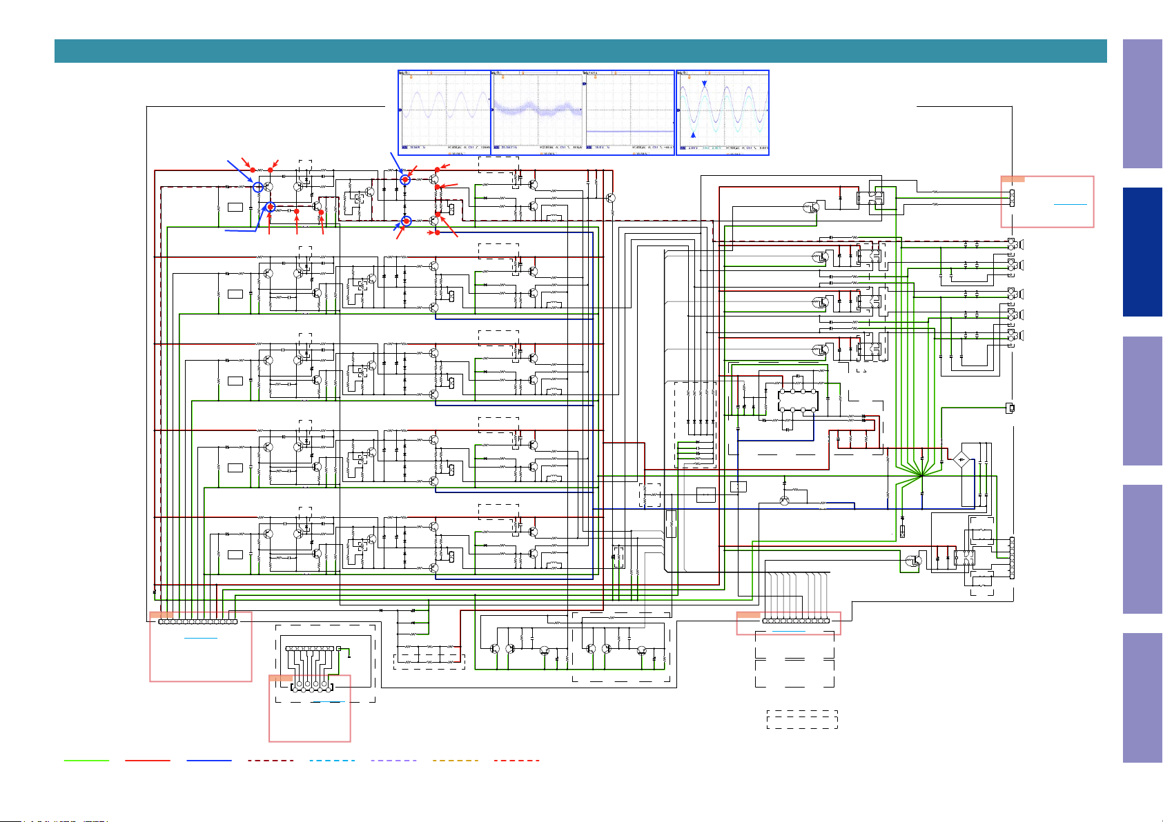
SCH06 MAIN AMP
MAIN PART
FL_IN
SL_IN
CEN_ IN
C5723
50V/10uF
BN501
1 2 3 4 5 6 7 8 9
TO CN772
4.AGND
2.AGND
5.CEN
3.SL
1.FL
TO DIGI TAL B 'D
INP UT/V OLU ME PA RT
2.0 mm 13PIN W IRE
6.AGND
Point A
Point B
SR_IN
8.AGND
7.SR
FR_IN
9.FR
LEFT FRONT -CH
C5101
50V/47uF
100K
R5101
LEFT SURROU ND-C H
C5201
50V/47uF
100K
R5201
CENT ER-CH
C5301
50V/47uF
100K
R5301
RIGHT SURRO UND -CH
C5401
50V/47uF
100K
R5401
RIGHT FRO NT-C H
C5501
50V/47uF
100K
R5501
10 11 12 13
10.+12V
11.RLY _GND
12V
CEN
12.MUT E_+ B
R5102
680
FL
R5202
680
SL
R5302
680
R5402
680
SR
R5502
680
FR
DGND
MUTE _+B
BN501
13.DGND
0.6V
D5101
R5103
10K
R5104
C5102100V /1000pF(M )
R5105 1.2K
-50.3V -51.0V -50.8V
R5203
10K
R5204
C5202100V /1000pF(M )
R5205 1.2K
R5303
10K
R5304
C5302100V /1000pF(M )
R5305 1.2K
R5403
10K
R5404
C5402100V /1000pF(M )
R5405 1.2K
R5503
10K
R5504
C5502100V /1000pF(M )
R5505 1.2K
OPEN
R5108 470K
C5103
C5106 33P
82P
Q5101
R5109 33K
KSA992FT A
Q5102
KSA992FT A
18K
18K
18K
18K
18K
C5105
50V/220uF
C5104
R5107
2200pF
220
R5106
1.2K( 1W)
J5101
OPEN
D5201
OPEN
R5208 470K
C5203
C5206 33P
82P
Q5201
R5209 33K
KSA992FT A
Q5202
KSA992FT A
C5205
50V/220uF
C5204
R5207
2200pF
220
R5206
1.2K( 1W)
J5201
OPEN
D5301
OPEN
R5308 470K
C5303
C5306 33P
82P
Q5301
R5309 33K
KSA992FT A
Q5302
KSA992FT A
C5305
50V/220uF
C5304
R5307
2200pF
220
R5306
1.2K( 1W)
J5301
OPEN
D5401
OPEN
R5408 470K
C5403
C5406 33P
82P
Q5401
R5409 33K
KSA992FT A
Q5402
KSA992FT A
C5405
50V/220uF
C5404
R5407
2200pF
220
R5406
1.2K( 1W)
J5401
OPEN
D5501
OPEN
R5508 470K
C5503
C5506 33P
82P
R5509 33K
Q5501
KSA992FT A
Q5502
KSA992FT A
C5505
50V/220uF
C5504
R5507
2200pF
220
R5506
1.2K( 1W)
J5501
OPEN
TU NER M ODU LE
TU500 YST990- A9U2
1 2 3 4 5 6 7 8
BN508
BN508
C125Z1-0 9
TO TU771
9.L-O UT
8.R-O UT
7.VC C
6.SCL K
5.SD IO
TO DIGI TAL B 'D
9P IN B'D TO B'D
Point A Point B
Point C1
1.10V
R5116
R5115
5.6K( 1W)
5.6K( 1W)
C5107
-1.10V
5.6K( 1W)
C5207
OPEN
5.6K( 1W)
C5307
OPEN
5.6K( 1W)
C5407
OPEN
5.6K( 1W)
C5507
OPEN
D5704
1SS133MT
R5117
4.7(1 W)
D5102
OPEN
D5103
C5108
50V/47uF
63V/100uF
OPEN
R5121
R5119
0.47(2W )
0.47(2W )
D5104
OPEN
R5122
R5120
0.47(2W )
0.47(2W )
D5105
R5118
OPEN
4.7(1 W)
-53.4V
R5216
R5215
5.6K( 1W)
R5217
4.7(1 W)
D5202
OPEN
D5203
C5208
50V/47uF
63V/100uF
OPEN
R5221
R5219
0.47(2W )
0.47(2W )
D5204
OPEN
R5222
R5220
0.47(2W )
0.47(2W )
D5205
OPEN
R5218
4.7(1 W)
R5315
R5316
5.6K( 1W)
R5317
4.7(1 W)
D5302
OPEN
D5303
C5308
50V/47uF
63V/100uF
OPEN
R5321
R5319
0.47(2W )
0.47(2W )
D5304
OPEN
R5322
R5320
0.47(2W )
0.47(2W )
D5305
OPEN
R5318
4.7(1 W)
R5415
R
5416
5.6K( 1W)
R5417
4.7(1 W)
D5402
OPEN
D5403
C5408
50V/47uF
63V/100uF
OPEN
R5421
R5419
0.47(2W )
0.47(2W )
D5404
OPEN
R5422
R5420
D5405
OPEN
R5515
50V/47uF
D5505
OPEN
C5508
OPT.
5.6K( 1W)
R5516
63V/100uF
R5715
2.2K( 1W)
R5718
OPEN
D5502
OPEN
D5503
OPEN
C5717
50V/10uF
D5703
R5714
0.47(2W )
0.47(2W )
R5418
4.7(1 W)
R5517
4.7(1 W)
R5521
R5519
0.47(2W )
0.47(2W )
D5504
OPEN
R5522
R5520
0.47(2W )
0.47(2W )
R5518
4.7(1 W)
Z6.8V
OPEN
R5716
2.2K( 1W)
R5719
OPEN
Q5104
KTC3114A
2.7K/ F
R5113
Q5103
KSC1845FT A
515/F
R5133
VR510
OPEN
33
R5134
515/F
R5114
R5111 OPEN
R5112 OPENR5212 OPENR5312 OPENR5412 OPENR5512 OPEN
R5110
Q5203
KSC1845FT A
R5210
Q5303
KSC1845FT A
R5310
Q5403
KSC1845FT A
R5410
Q5503
KSC1845FT A
R5510
4./C E
3./RS T
47(1W)
47(1W)
47(1W)
47(1W)
47(1W)
Point C2
PRE_- B
Q5204
KTC3114A
2.7K/ F
R5213
515/F
R5233
VR520
33
R5234
515/F
R5214
R5211 OPEN
Q5304
KTC3114A
2.7K/ F
R5313
515/F
R5333
VR530
33
R5334
515/F
R5314
R5311 OPEN
Q5404
KTC3114A
2.7K/ F
R5413
R5433
515/F
VR540
33
R5434
515/F
R5414
R5411 OPEN
PRE_- B PRE_- BPRE_- B
Q5504
KTC3114A
2.7K/ F
R5513
515/F
R5533
VR550
33
R5534
515/F
R5514
R5511 OPEN
+12V
DGND DGND
AGND AGND
PRE_- B
MUTE _+B
CHASSI S
123456789
2.INT
1.CH _GND
Q510
KTD 1630G
CN510
CA2505-W V02L
Q5106
KTB2630G
Q5205
KTD 1630G
CN520
CA2505-W V02L
Q5206
KTB2630G
Q5305
KTD 1630G
CN530
CA2505-W V02L
Q5306
KTB2630G
Q5405
KTD 1630G
CN540
CA2505-W V02L
Q5406
KTB2630G
Q5505
KTD 1630G
CN550
CA2505-W V02L
Q5506
KTB2630G
R5717
2.2K( 1W)
R5720
OPEN
PTC T herm ist ors
R5126
53.4V
DHP TF1608471P85T / 85'C
5
R5123
2mV
820K
D5106
R5124
1SS133MT
21
R5125 10K
-2mV
PTC T herm ist ors
R5226
DHP TF1608471P85T / 85'C
R5223
820K
D5206
R5224
1SS133MT
21
R5225 10K
PTC T herm ist ors
R5326
DHP TF1608471P85T / 85'C
R5323
820K
D5306
R5324
1SS133MT
21
R5325 10K
PTC T herm ist ors
R5426
DHP TF1608471P85T / 85'C
R5423
820K
D5406
R5424
1SS133MT
21
R5425 10K
PTC T herm ist ors
R5526
DHP TF1608471P85T / 85'C
R5523
820K
D5506
R5524
1SS133MT
21
R5525 10K
AGND
-B
AGNDAGND
PRE_- B
+B +B
DC_F RONT
Q5703
KTC3875S YRT K
DC PRO TECT ION
150K
150K
150K
150K
150K
R5127
5.6K
R5227
5.6K
R5327
5.6K
R5427
5.6K
R5527
5.6K
KTA1504S YRT K
Q5107
0.1uF
C5109
MMBTA9 2
R5129 15K
R5130 22K
Q5108
MMBTA4 2
R5131 22K
L5101
R5128
OPEN
R513210(1W )
Q5207
0.1uF
C5209
MMBTA9 2
R5229 15K
R5230 22K
Q5208
MMBTA4 2
R5231 22K
L5201
R5228
OPEN
R5232 10(1 W)
Q5307
0.1uF
C5309
MMBTA9 2
R5329 15K
R5330 22K
Q5308
MMBTA4 2
R5331 22K
L5301
R5328
OPEN
R5332 10(1 W)
Q5407
0.1uF
C5409
MMBTA9 2
R5429 15K
R5430 22K
Q5408
MMBTA4 2
R5431 22K
L5401
R5428
OPEN
R5432 10(1 W)
Q5507
0.1uF
C5509
MMBTA9 2
R5529 15K
R5530 22K
Q5508
MMBTA4 2
R5531 22K
L5501
R5528
OPEN
R5532 10(1 W)
100K
0.1uF
C5710
R5705
KTC3875S YRT K
Q5704
C5701
0.01uF
R5701 10K
Q5701
MMBTA9 2
0.5UH
0.5UH
0.5UH
DC_D ET DC_D ET DC_D ET
0.5UH
DC_D ET
0.5UH
R5728
OPEN
Q5705
10K
C5711
R5706
6.3V/ 470uF
22K
R5702
FL_OU T
THEMAL DET _A
THEMAL DET _ATHEMAL DET _A
ASOASOASO ASO
THEMAL DET _B
THEMAL DET _A
FR_OU T
-B
+12V+12V+12V
RLY_ GNDRLY_GNDRLY_ GNDRLY_ GND
DGND
AGND
PRE_- B
Q5706
OPEN
SL_O UT
AGNDAGNDAGND
FR_OU T
CEN_ OUT
SR_O UT
SL_O UT
+B +B+B+B
FR_OU T
CEN_ OUT
SR_O UT
ASO_ DET
_DET A SO_D ET
FR_OU T
SR_O UT
+B
33K
R5819
R5817
33K
R5818
POWE R DE T.
B+/B -
ASO_ DET ASO
AGND
FR_OU T
-B -B -B -B
THER MALDE T_A
THER MALDE T_B
ASO_ DET
DC_P ROT
2.2K
R5711
C5716 16V/ 47uF
5713 2.2K
R
R5712 2.2 K
R5729
OPEN
Q5708
OPEN
OPEN
R5707
C5712
OPEN
7
Q570
OPEN
B+ /B- POW ER D ETEC T
Point C1
Point C
Measurement condition
・Voltage measurement
No signal
・Waveform measurement
INPUT: 200mVrms / 1KHz (ANALOG)
Point C2
Surround mode: MCh Stereo
VOL: 70
Speaker load: 8ohms
RY560
Q5601
KRC105S
KRC105S
KRC105S
CURREN T_D ET
8.NC
8.CURRE NT_D ET
C5718 0.047uF
Q5602
C5719 0.047uF
C5720 0.047uF
Q5603
C5721 0.047uF
C5722 0.047uF
Q5604
R5836
OPEN
R5837
OPEN
5678
R5703 33(1 W)
J5604
ASO_ DET
THER MALDE T_A
10 1 1
9.ASO _DE T
10.THE RMALDE T_A
9.ASO _DE T
10.THE RMALDE T_A
HFD27/ 012-H
2
D5601
C5601
C5602
C5603
OPEN
R5838
C5824
J5602
C5828
1SS133MT
R5721 10(2 W)
OPEN
D5602
R5722 10(2 W)
R5723 10(2 W)
OPEN
D5603
R5724 10(2 W)
R5725 10(2 W)
D5604
OPEN
OPEN
R5839
OPEN
R5840
OPEN
R5827
JUMPE R
5643817
RY562
32451
6
1SS133MT
RY563
32451
6
1SS133MT
32451
6
1SS133MT
RY564
981-21-12DS
RY562
RY563
981-21-12DS
RY564
981-21-12DS
C5825
OPEN
C5826
OPEN
OPEN
OPEN
R5826
R5709
R5710
AGND
RLY_ GND
THER MALDE T_B
11.THE RMALDE T_B
11.THE RMALDE T_B
R5726
H/P_ FR
470(2W)
R5727
H/P_ FL
470(2W)
FL_OU T
C5605
0.018uF
FR_OU T
C5606
0.018uF
C5608
C5607
2200pF
2200pF
SL_O UT
C5609
0.018uF
SR_O UT
C5610
0.018uF
CEN_
C5611
0.018uF
OUT
C5612
C5613
C5614
2200pF
2200pF
OPEN
J5601
C5704
63V/6800uF
2
OPEN
OPEN
C5707
50V/0.1 uF
ET501
CHASSI S
Q5806
KRC105S
1
OPEN
C5615
3
D5701
D25SB6 0
C5706
63V/6800uF
4 351
D5806
OPEN
C5801
1SS133MT
+12V
OPEN
D5816
R5831
100V/100uF
Q5702
KSA992FT A
R5834
OPEN
OPEN
OPEN
IC501
OPEN
R5832
OPEN
C5821
C5708
KRC105S
FL_OU T
FR_OU T
SL_O UT
SR_O UT
CEN_ OUT
C5823
OPEN
R5835
OPEN
1 2 3 4
R5833
OPEN
OPEN
R5704
100(1W)
FL_OU T
CEN_ OUT
FR_OU T
SL_O UT
SR_O UT
H/P_ RLY
FRONT _RLY
MCU_ CTL
C/S_ RLY
C/S_ RLY
CURREN T_D ET
R5814 O PEN
R5815 O PEN
LEVE L DE T.
D5811 O PEN
D5810 O PEN
D5807
C5806 O PEN
C5807 O PEN
R5810
R5811
DGND
33K
R5821 OP EN
RLY_ GND
CURREN T_GND
+12V
OPEN
R5816
R5813 O PEN
D5809 O PEN
D5812 O PEN
OPEN
OPEN
OPEN
J5821
JUMPE R
-B
OPEN
R5830
R5812 O PEN
D5808 O PEN
OPEN
OPEN
C5819
D5815
C5817 OP EN
C5820
OPEN
C5818
-12V
AGND
OPEN
J5822
PRE_- B
-12V
HI-B _RLY
AMPSIG_ DET
+12V
RLY_ GND
PRE_- B
BN502
OPEN
OPEN
C5713
R5708
S500 S eries
S600 S eries
C/S_ RLY
H/P_ RLY
FRONT _RLY
AMPSIG_ DET
1 2 3 4 5 6 7 8 9
BN502
TO CN712
3.FRO NT_R LY
4.C/S _RLY
1.HI- B_RL Y
2.H/ P_RL Y
5.NC
3.FRO NT_R LY
4.C/S _RLY
2.H/ P_RL Y
1.HI- B_RL Y
5.AMPSIG _DE T
TO DIGI TAL B 'D
MC U PAR T
2.0 mm 11PIN W IRE
PTC T herm ist ors
THER MALDE T_A
THER MALDE T_B
DC_P ROT
B_DE TEC T
6.DC _PRO T
6.DC _PRO T
FL-CH , SL- CH, C EN_C H
FR-CH , SR-C H
7.B_D ETE CT
7.-12V
BN505
1
1.HP _RCH
2
2.AGND
TO CN104
3
3.HP _LCH
BN505
TO FRON T B'D
2.0 mm 3PIN WIRE
C5616
1
OPEN
C5617
OPEN
C5618
OPEN
C5619
OPEN
C5620
OPEN
2200pF
OPEN
4
250V/0.1 uF
C5714
C5702
OPEN
250V/0.1 uF
C5703
C5715
F5801
OPEN
J5804
JUMPE R
RY586
HF115F/012
726 8
J5805
JUMPE R
F5802
OPEN
2
1
2
1
2
1
2
1
2
BK051
CMD1 A569-V1
M3 BR ACK ET
CN503
CJP07GA 90ZY
JK501
CJJ5N032Z D
JK502
CJJ5N032Z D
JK504
CJJ5N032Z D
JK505
CJJ5N032Z D
JK503
CJJ5N032Z D
7 6 5 4 3 2 1
FL-CH
FR-CH
SL-CH
SR-CH
C-CH
AC_L
N.C
AC_H
CEN
AC_H
N.C
AC_L
FRO M MAIN T RAN S
3.96mm 7 PIN W AFE R
This Unit
Before Servicing
Electrical Mechanical Repair Information Updating
GND LINE
POWER+ LINE
POWER- LINE
ANALOG AUDIO
DIGITAL AUDIO
TMDS SIGNAL
ANALOG VIDEO
STBY POWER
14
Page 15
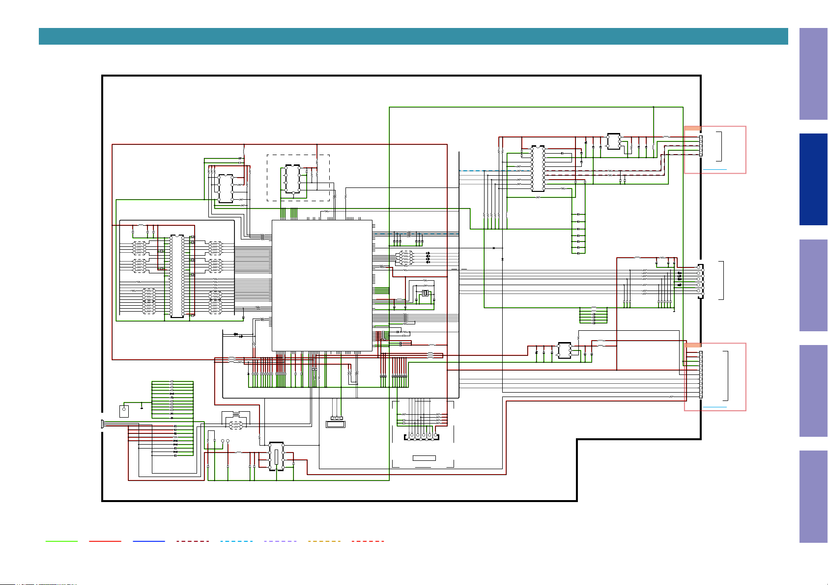
SCH07 USB, BT
USB / BT PA RT
L2004
220R/2A
C2019
C2020
C2018
16V/1uF
10V/0.1u F
RN2008 33x 4
DQ15
1234
5678
DQ14
DQ13
DQ12
RN2007 33x4
DQ11
1234
5678
DQ10
DQ09
DQ08
R2027
UDQM
CLK
33
CKE
RN2006 33x4
R2097
A12
A11
OPEN
A09
A08
1 2 3 4
CHASSI S
1234
RN2005 33x4
5 6 7 8
5678
4.D GND
3.US BD+
2.US BD-
1.VB US
A07
A06
A05
A04
META L PLA TE
4321
JK201
This Unit
Before Servicing
IC2004
BU33TD 3WG
DA+3 V3
15
VIN
VOUT
2
IC2003
CVIPCM 5102APW R
DVD D
CPVD D
C2006
CAPP
DGND
C2004
16V/0.1u F
LDOO
C2005
XSMT
16V/0.1u F
FMT
LRCK
0
DIN
BCK
SCK
FLT
13 14 2019181716151211
R2021 0
6.3V/2 .2uF
R2022
TLV75712P DBV R
OUT
NC
423
6.3V/10u F
C2008
16V/0.1u F
C2009
6.3V/2 .2uF
C2007
C2010
16V/0.1u F
10K
C2039
16V/0.1u F
C2042
16V/0.1u F
C2041
1uF
16V/0.
C2040
16V/0.1u F
C2125
16V/0.1u F
C2126
50V/0.01uF
C2127
50V/1000pF
IC2007
100
R2073
IN
15
GND
EN
C2102
CPGND
CAPM
VNEG
OUTL
OUTR
AVDD
AGND
9 8 7 6 5 4 3 2 1
DEMP
10
OPEN
C2099
C2101
C2100
16V/0.1u F
1K
2.2M
4
L2009
220R/2A
MCS_RST
R2086 10K
R2087 10K
R2088 10K
R2085 10K
4.DGND
3.RES ET
MLC3730
MCS_LRC K
MCS_DIN
MCS_BC LK
MCS_MC LK
USB_OC P_D ET
DEBUG_ RX
MCS_MC LK
MCS_LRC K
MCS_BC LK
MCS_DIN
BT_TX
BT_RX
BT_CTS
BT_RTS
DEBUG_ TX
BT_RST BT_RST
BT_CTS
BT_RTS
BT_RX
BT_TX
BT_SCL
BT_SDA
C2038
50V/12pF
PRTCK
PTCK
PTDI
PTDO
PTMS
PNTRST
MCS_RST
220R/2A
220R/2A
220R/2A
MCS_TX
MCS_RX
MCS_RST
1234567
1
CN214
CJP10GB 310ZY
1.VCC
2.GND
R2016 10K
R2018 0
R2019
R2017 0
R2020 0
OPEN
OPEN
L2006
R2063 0 R2015 OP EN
R2062 OP EN
R2061 OP EN
R2060 OPE N
R2059
KDS160
D2001
KDS160
D2008
L2002
60R/3A
C2001
16V/22uF
C2002
50V/0.1u F
10K
IC2001
MX25L1606EM 2I-12G
1234
R2001
CS#
R2003 10K
R2002 4.7K
VCC
R2004
SO
HOL D#
WP#
SCLK
5 6 7 8
SI
GND
IC2005
W9812G6K H-6
D2002
D2006
D2007
C2129
C2128
C2105
C2106
C2107
C2132
C2131
C2130
C2108
C2109
C2110
C2111
R2082 2.2 K
D2003
D2004
C2112
D2005
C2104
545352515 049484746454443424140393837363534333231302928
DQ11
VSSQ
DQ10
A10/AP
16V/0.1u F
16V/0.1u F
OPEN
50V/0.1u F
KDS160
KDS160
VDD
VSS
DQ0
DQ15
VDDQ
VSSQ
DQ1
DQ14
DQ2
DQ13
VSSQ
VDDQ
DQ3
DQ12
DQ4
VDDQ
DQ5
DQ9
DQ6
VSSQ
VDDQ
DQ7
DQ8
VDD
VSS
LDQM
NC
UDQM
/WE
CLK
/CAS
CKE
/RAS
NC
/CS
A11
BA0/A1 3
A9
BA1/A1 4
A8
A0
A7
A1
A6
A2
A5
A3
A4
VDD
VSS
OPEN
OPEN
CDS3C 05HD MI1
OPEN
OPEN
OPEN
OPEN
50V/0.1u F
6.3V/220u F
CDS3C 05HD MI1
CDS3C 05HD MI1
OPEN
CDS3C 05HD MI1
OPE
C2023
10V/0.1u F
RN2001 33x4
DQ00
1234
RN2002 33x4
1234
R2029 33
R2028
R2033 33
R2032 33
R2031 33
RN2003
33x2
4 3
R2030 33
1234
RN2004 33x4
R2083 100
16V/0.1u F
C2116
5678
CAS
DQ01
RAS
UDQM
DQ02
LDQM
BA1
DQ03
BA0
A12
A11
A10
A09
A08
DQ04
5678
A07
A06
DQ05
A05
A04
DQ06
A03
A02
DQ07
A01
A00
LDQM
DQ15
DQ14
WE
DQ13
33
DQ12
CAS
DQ11
DQ10
RAS
DQ09
DQ08
CS
DQ07
DQ06
BA0
DQ05
DQ04
BA1
DQ03
2 1
DQ02
A10
DQ01
DQ00
A00
5678
A01
CKE
A02
CLK
CS
A03
WE
MCS_TX
MCS_RX
L2011
220R/2A
L2012
220R/2A
L2013
OPEN
R2074
L2017
OPEN
43
RN2010
T2002
T2003
16V/0.1u F
C2113
L2018
220R/2A
16V/0.1u F
C2117
C2027
10V/0.1u F
C2025
9 8 7 6 5 4 3 2 1
10V/0.1u F
C2024
10V/0.1u F
C2026
2726 25 24 232 22 120 19 18 17 16 15 141 31 211 10
10V/0.1u F
N
6.3V/22u F
C2022
10V/0.1u F
C2021
10V/0.1u F
5.1K
R2005
33
R2026
4.7K
C2028
OPEN
21
0x2
VDD33IO
VDD33USB
VDD30RTC
R2007
OPEN
R2006
R2034
R2035
OPEN
OPEN
D2009
16V/0.1u F
C2118
Au th 3 .0 CP (XD FN)
10K
A12
R2039 33
B12
R2036 33
B11
R2037 33
A11
R2038 33
A3
J17
J16
L17
L16
E14
F16
T17
R17
F17
R16
P16
P17
N17
N16
N14
K16
G16
G17
H17
A17
B17
C17
C16
D16
D17
E17
E16
A13
B13
B14
A14
A15
B15
B16
A16
M16
75
M17
75
K17
H16
T15
P6
R2093 33
P7
R2094 33
N7
P8
P10
P11
R2095 10K
R2096 10K
F
6.3V/22u F
10V/0.1u F
6.3V/22u F
10V/0.1u
10V/0.1u F
10V/0.1u F
50V/0.01uF
50V/0.01uF
50V/0.01uF
C2075
C2070
C2073
C2069
C2074
C2072
C2071
C2068
C2067
USB_OC P_D ET
10K
IC2008
R2013
TPS2069CD GNR
/FLT
OUT
OUT
10V/1uF
8 7 6 5
OUT
C2119
PGPA00
PGPA01
PGPA02
PGPA03
PGPA04
PSDCAS N
PSDRAS N
PSDDQM[1]
PSDDQM[0]
PSDBA[ 1]
PSDBA[ 0]
PAD[12]
PAD[11]
PAD[10]
PAD[9]
PAD[8]
PAD[7]
PAD[6]
PAD[5]
PAD[4]
PAD[3]
PAD[2]
PAD[1]
PAD[0]
PD[15]
PD[14]
PD[13]
PD[12]
PD[11]
PD[10]
PD[9]
PD[8]
PD[7]
PD[6]
PD[5]
PD[4]
PD[3]
PD[2]
PD[1]
PD[0]
PSDCKE
PSDCLK
PSDCSN
PSDWEN
PGPE14
PGPE01
PGPE02
PGPE03
PGPE04
PGPE05
PGPE06
VDD33IO-4
VDD33IO-5
P4
D4
16V/0.1u F
16V/0.1u F
16V/0.1u F
C2076
C2077
C2078
EN
IN
IN
GND
IC2002
CVI23671051550AS_ DM
4 3 2 1
J5
J13
T4
B9
VSS12INT
VSS12CORE-2
VSS12CORE-1
VSS12CORE-3
VDD33IO-3
VDD30RTC
VDD12ALIVE
VDD33IO-2
VDD33IO-1
P14
T16
A10
T10
D14
OPEN
16V/0.1u F
16V/0.1u F
16V/0.1u F
C2082
C2081
C2079
C2080
4321
0
R2009
8765
GND
Vcc
C2003
10V/0.1u F
GND
R2010 4.7K
R2008 4.7K
NC NC
SCL
GND
SDA
Apple 3. 0 aut hent icat ion
9
N5
A1
B2
E5
A2
B3
N13
E13
B10
3
PGPA08
PGPA07
PGPA06
PGPA05
VSS33IO-2
VSS33IO-
VSS33IO-5
VSS33IO-1
VSS33IO-4
CVIM LC3730S_ J
VDD33USB20-2U7PUDP20
PUVBUS 20T7VSS33USB20-2T8PRTUNE2 0
VDD33USB20-1
PUDN20
PUDN11A8PUDP11
VSS33USB20-1
VDD12USB20
VDDUSB11B8VSSUSB11
P9
A7
T9
B7
U6
U5
U8
16V/0.1uF
16V/0.1uF
16V/0.1u F
16V/0.1u F
C2086
C2085
44.2/F
C2083
C2084
R2076
C2120
10V/1uF
PGPE07
IC2006
PGPB08
T6
OPEN
R2078
33
R2014
R2012 3 3
R2011 3 3
R2048
33
5
L4
H14
G14
PGPD09
PGPD10
D20
PUI
VSS12USB20
T5
N9
OPEN
CN416
DE BUG
K14
PGPD08
PGPD07
PWAKEU P
U15
DEBUG_ RX
1 2 3
T3
K4
T1
U1
U2
L
U3
L13
L14
M14
PGPD06
PGPD05
PGPE11
PGPE10-PRE MOC O
PGPE12
PGPE13
T13
T14
U13
U14
DEBUG_ TX
C2
PGPA11
B1
PGPC07
PGPC08
PGPC13
PGPC11
PGPC12
PGPC09
PGPC14
PGPC10
PGPA09
C1
PGPA10
D2
D1
E1
E2
E4
R2
F2
F1
G1
G2
H2
T2
K1
L1
L2
M2
G5
H1
R2040 4.7K
J1
R2092 4.7K
H4
K2
M1
N1
N4
N2
P2
P1
R1
B5
A5
A6
B6
D5
U9
U11
U10
U12
U17
U16
D6
D7
D9
E7
D8
D10
T11
T12
E9
A9
J4
J14
U4
P12
A4
B4
P13
R2055 47
R2053 47
R2054 47
R2052 100
OPEN
OPEN
OPEN
50V/33pF
50V/33pF
50V/33pF
C2032
C2031
C2029
C2035
C2036
C2034
RN2009 33x4
1 2 3 4
5 6 7 8
R2047 33
33
R2049
R2056
R2057
1
2 3
L2005
X2001
220R/2A
VDD33OSC
16V/0.1uF
C2056
16V/0.1uF
C2057
16V/0.1uF
C2058
16V/0.1uF
C2059
16V/0.1uF
C2060
C2061
16V/0.1uF
6.3V/22u F
10V/0.1u F
50V/0.01uF
C2089
C2090
C2091
C2030
6.3V/22u F
C2092
16V/1uF
R2041
R2042 33
R2043 33
R2044 33
R2045 33
R2046 100
R2050 2.2K
C2062
OPEN
C2064
C2065
10V/0.1u F
50V/0.01uF
C2093
C2094
24MHz/8 pF
C2037
50V/12pF
C2033
10V/0.1u F
100
R2072
100
10V/0.1u F
C2063
6.3V/22u F
VDD33ADC
16V/0.1u F
L2016
VDD12PLL
L2015
VDD12USB 20
VDD12ALIV E
L2014
10V/0.1u F
10V/0.1u F
50V/0.01uF
50V/0.01uF
C2098
C2095
C2096
C2097
PTDI
PTCK
PTMS
PTDO
PRTCK
PNTRST
R2084
OPEN
C2115
50V/10pF
C2114
50V/10pF
8910
9
10
8765432
7.PTM S
9.PTD O
6.PTD I
8.PTC K
5.PNT RST
10.PRTC K
for DEBU G
MP => OPEN
PA12
PG
PGPA13
PGPA14
PGPA15
PGPB00
PGPC05
PGPB01
PGPB02
PGPB03
PGPB04
PGPB05
PGPC06
PGPB10
PGPB11
PGPB12
PGPB13
PGPD13
PGPB06(B OOT[0]
PGPB07(B OOT[1]
PGPD15
PGPB09
PGPB14
PGPB15
PGPC00
PGPC01
PGPC02
PGPC03
PGPC04
PAIN[0]
PAIN[1]
PAIN[2]
PAIN[3]
PAIN[4]
VDD33OSC
PXO
PXI
VSS33OSC
PRTCXO
PRTCXI
PRTCK
PTCK
PTDI
PTDO
PTMS
PNTRST
PTEST
PRESETN
VDD12CORE-1
VDD12CORE-2
VDD12INT
VDD12CORE-3
VDD12CORE-4
VDD12PLL
VDD33ADC
VSS33ADC
VSS12PLL
PGPD04
PGPD12
PGPD11
PGPD02
PGPE00
PGPD03
PGPC15
PGPD01
PGPD00
F4
P5
M4
F14
E11
G13
D11
D12
D13
10K
10K
R2090
R2091
R2080 33
R2081 33
BT_SCL
BT_SD A
G4
N11
PGPD14
J2
GND
OPEN
C2011
4
3
STBY
NC
10K
C2013
C2012
6.3V/10u F
16V/0.1u F
R2024 470
R2023 470
C2014
6.3V/10u F
L2007
L2020
C2123
C2124
C2121
C2122
16V/0.1u F
50V/2200pF
60R/3A
60R/3A
50V/1000pF
50V/0.01uF
50V/1000pF
50V/0.01uF
L2019
OPEN
L2010
220R/2A
C2103
6.3V/10u F
L2003
C2017
C2016
R2025
OPEN
6.3V/10u F
16V/0.1u F
C2015
50V/2200pF
L2008
220R/2A
C2046
R2070 100
R2067 22
22
R2068
R2069 33
R2064 33
R2066 33
R2065 33
OPEN
OPEN
OPEN
C2044
C2043
C2045
BN211
L2021
BN211
60R/3A
1234
1.+ 5VA
2.D A_GND
3.US B/BT _R
4.D A_GND
5
5.US B/BT _L
TO CN752
TO DIGIT AL B 'D
WI RE/5 P/2. 0mm
DIG ITAL POW ER PA RT
Electrical Mechanical Repair Information Updating
R2071
2.2
C2051
10V/0.1u F
50V/10pF
50V/10pF
50V/10pF
50V/10pF
C2053
C2052
C2050
C2049
R2089 0
CN213
C2054
10V/10uF
10V/0.1u F
1
1.VD D
2
2.RE SET
3
3.RT S
4
4.CT S
5
5.TX D
6
6.BT _GND
7
7.RX D
8
8.BT _GND
9
9.I2C _SC L
10.I2C_ SDA
10
1
1.D 5V
2
2.D 5V
34
3.D GND
4.D GND
5
5.US B3V3
67
6.US B_PO WER 1
7.MC S_T X
8
8.MC S_RX
9
9.MC S_RS T
10.USB _DA C_MU TE
1011
11.USB _EN
TO BT M ODU LE
MC U PAR T
WI RE/11P /2.0 mm
TO DIGIT AL B 'D
10V/0.1u F
C2055
BT_GND
BN212
BN212
TO CN713
GND LINE
POWER+ LINE
POWER- LINE
ANALOG AUDIO
DIGITAL AUDIO
TMDS SIGNAL
ANALOG VIDEO
STBY POWER
15
Page 16
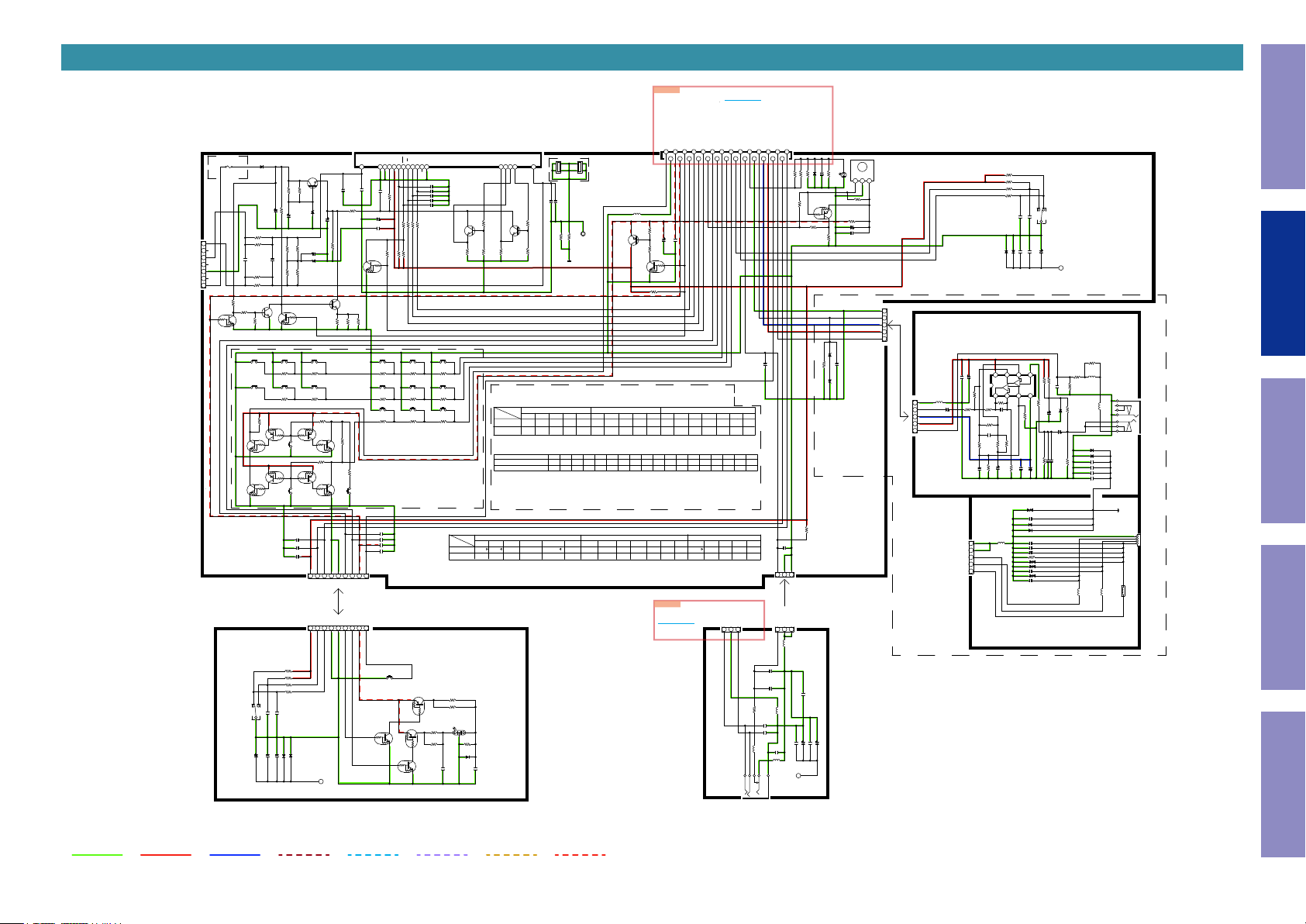
SCH08 FRONT
BN12B1
FRONT PART
T 315mA L 250V
D1001
1N4007
F1001
R1001
7. FL_AC
6. NC
CA2505-WR07L
5. FL_AC
4. NC
3. GND
FROM TRANS
2. NC
1 2 3 4 5 6 7
CN102
2.5mm 7PIN WAFER
1. VDISP
1.8(AXIAL)
R1002
OPEN(AXIAL)
OPEN
C1001
R1003
OPEN(AXIAL)
R1004
1.8(AXIAL)
KTC3875SYRTK
220K
R1428
R1429
Q1015
10K
R1430
KRC104S
SW102
SW108
RED_LED
W/G_LED
Q1017
OPEN
Q1021
OPEN
CUP12957Z-3
B
VR102
CSR2A060Z
12CLICK
ENCODER
FUNCTION
(SMALL)
OPEN
C1429
KTC1027YT
OPEN
R1007
R1062
10K(AXIAL)
27K(1/4W)
63V/100uF
C1006
50V/1uF
C1005
R1424
220
220
50V/10uF
R1006
R1009
(SMALL)
C1002
D1003
100V/0.1uF
220
220
R1005
R1008
Q1016
Q1013
22K
KRC102S
SW103
R1071
5.6k
SW109
R1076
5.6k
OPEN
R1091
Q1018
Q1019
OPEN
OPEN
SW115
Q1023
Q1022
OPEN
OPEN
SW116
C1087
OPEN
C1086
OPEN
C1085
OPEN
BN101_1
2.0mm 9PIN WIRE
2.0mm 9PIN WIRE
BN101
10K
R1413
R1414
10K
R1415
1K
R1416 1K
A
0.01uF
0.01uF
C
C1425
C1426
KDS160
KDS160
0.047uF
1000pF
D1406
D1407
C1428
C1427
FL101
CFLCIG251801N
F2
Q1001
D1005
SW104
R1072
3.3k
SW110
R1077
3.3K
1. +3V3
1. +3V3
57 53 52 51 50 49 48 47 46 45 44 43 8 7 6 5 1
C1007
OPEN
C1423
OPEN
R1030
Z39V
10(AXIAL)
C1010
C1004
50V/1uF
C1011
R1423
47K(AXIAL)
C1003
Z6.8V
Q1014
KTC1027YT
OPEN
1W/10
1W/10
R1427
R1426
R1425
R1090
0
Q1020
3.3K
R1082
OP
EN
R1092
0
5.6K
R1081
Q1024
SW114
OPEN
4. DGND
5. DGND
2. ISEL_A
3. ISEL_B
6. W/G_LED
7. RED_LED
9. POWER_KEY
8. MCU+5
987654321
987654321
5. DGND
4. DGND
2. ISEL_A
3. ISEL_B
8. MCU+5
7.RED_LED
6. W/G_LED
9. POWER_KEY
LUG14
CHASSIS
WIRE
NP
(SMALL)
Q1002
C1088
C1089
C1090
C1091
KRC102S
GND
C1009
16V/47uF
OPEN
SW105
R1073
2.7K
SW111
R1078
2.7K
SW117
R1083
2.7K
ON/STANDBY
Q1009
VFL
VDD
VDDH
10(AXIAL)
0.1uF/50V
R1067
0.1uF
39K
0
R1068
R1010
*OPTION
OPEN
OPEN
OPEN
OPEN
SW101
KRC102S
CP
CS
DA
OSC
RESET
100
100
R1014100
R1015
R1012100
R1013
R1011 OPEN
SW106 SW107
R1074
1k5
SW112
R1079
1k5
SW118
R1084
1k5
Q1008
KRA102S
Q1011
KRA102S
Q1012
NX
TSA
TSB
OPEN
C1012
100P
C1013
100P
C1014
330P
C1015
1000P
C1016
R1075
1K
KEY1
SW113
R1080
1K
KEY2
SW119
R1085
1K
KEY3
18G
R1018
Q1003
KTC3875SYRTK
Q1004
39K
39K
100K
R1025
R1016
R1026
+3V3
*OPTION
AVR-S570BT/X580BT RESISTOR VALUE
AVR-S570BT
AVR-X580BT
KEY OPTION
KEY NAME
SW102 SW110 SW111
ADJUST ADJUST
TUNE+
STATUS
-
G
SB-LED
R1045
OPEN
D1002
OPEN
C1055
0.1uF
R1043
R1044
OPEN
4.7K
R1041 1.2K
R1042 1.2K
C1054
0.1uF
AVR-S570BT
AVR-X580BT
D1012
R
PCB BRAKET
BK101
BK102
F1
NP
17G
Q17G
Q18G
1 2
1 2
3 4
3 4
CMD1A572
CMD1A572
OPEN
OPEN
C1041
C1017
R1019
KTC3875SYRTK
OPEN
OPEN
BN10
OPEN
STYLE PIN
R1086
R1087
100K
R1017
CHGND
BRACKET
KEY_1
KEY_2
KEY_3
1.5K2.7K
5.6K
3.3K
1K
1.5K
OPEN
OPEN
SW102 SW103 SW104 SW105 SW106 SW107 SW108 SW109 SW110 SW111 SW112 SW113 SW114 SW115 SW116 SW117 SW118 SW119
O
AVR-S570BT
AVR-X580BT
O O O O O O O O O O O O O O O O O
X
X
KEY_1 KEY_2 KEY_3
SW107SW105 SW114SW103 SW104 SW106 SW113SW108 SW116SW115SW112SW109
PRESET-
Q/S_1
SOUND
--
TUNE-
PRESET-
Q1005
R1076
1K
2.7K3.3K5.6K 2.7K3.3K5.6K
OPEN
1.5K
0
O O O
X X X X X X
ON/OFF
PRESET+
SLEEP
TUNE+
26.DGND
25.MCU_3V3
27. N.C
27
25 23
26 24
L1001
CB03YTYH600
1K
R1021
C1019
C1020
KTA1504SYRTK
50V/10uF
3.3K
R1020
Q1006
KRC102S
+3V3
R1422
OPEN
R1079 R1080R1077R1072 R1074 R1075 R1078R1073R1071
1K
1.5K
OPEN
001K 0
O O O O O O O
BASS/
Q/S_2
Q/S_4
STATUS
TREBLE
Q/S_4Q/S_2
2.0mm 3PIN WAFER
CN104
TO BN505
ENCODER&POWER
FROM DIGITAL B'D
1.25mm 27PIN FFC
19.FL_RST
17.W/G_LED
16.RED_LED
21.FL_CLK
23.CPU_POWER
22.FL_DATA
18.RC_IN
20.FL_CE
24.MCU_5V
17 1514131211
21 19
16
22 20
18
0.01uF
KEY_3KEY_2KEY_1
R1084 R1085
R1083R1082R1081
1K
1.5K
1.5K2.7K
1K
MODE
TUNE-
SOUND
DIMMER
PRESET+
--
Q/S_1
TO MAIN
CUP12957Z-4
TO CN711
12.VSEL_B
13.KEY_3
14.KEY_2
15.KEY_1
11.VSEL_A
10.H/P_DET
10
R1090 R1092
0
DIMMER
Q/S_3
CN104
3.HP_LCH
1.HP_RCH
2.AGND
CA2005-WV03-K
123
2
CJJ2E041ZD
JK104
2. HP_LCH
9.B/P_IRIN_DE
98765
0
00
SW119SW118SW117
Q/S_3
---
R1057
L1012
3. HP_RCH
8.AGND
7.MIC_SIGNAL
C1082
470
C1071
680P
C1072
680P
CB03YTYH600
873
7. DET
8. DGND
6.-12V
BN131
C1424
0.1uF
C1069
O
1
5.+12V
4 2
OPEN
PEN
C1083
OPEN
L1013
CB03YTYH600
12378
1. AGND
4.POWER_KEY
3.MIC_DET
3
C1081
0.1uF
3.H/P_DET
3.H/P_DET
3 2 1
L1010
B03YTYH600
C
2.DGND
L1011
HEADPHONE
BN12B1
2.ISEL_B
1.ISEL_A
CJP27GB286ZN1.25-2S-27PW
1
OPEN
OPEN
OPEN
R1420 OPEN
R1418
R1419
D1408
Q1007
1K
OPEN
R1069
R1022
OPEN
10K
R1046
CN103
1.DGND
CA2005-WR03-K
123
2.0mm 3PIN WAFER
2.0mm 3PIN WIRE
2.DGND
1.DGND
CB03YTYH600
01uF
C1084
0.
0.1uF
0.1uF
50V/1uF
50V/1uF
C1067
C1068
C1066
LUG13
CHASSIS
WIRE
RC101
37.9kHz
OPEN
C1430
R1023
(38kHz)
OPEN
Vcc
GND
VOUT
321
LD101
R1421 OPEN
OPEN
R1024
R1053
10
C1038
16V/47uF
(SMALL)
100P
C1039
OPEN
+3V3
D_GND
VOL-
VOL+
10K
R1061
R1060
10K
R1059
1K
1K
R1058
A
B
0.01uF
0.01uF
VR101
CSR2A055Z
C
C1077
C1076
VOLUME
24CLICK
0.1uF
OPEN
OPEN
C1073
D1015
D1016
ENCODER
(SMALL)
OPEN
OPEN
C1075
C1074
LUG11
CHASSIS
WIRE
This Unit
Before Servicing
CUP12957Z-1
1. AGND
BN12A
2. MIC_SIGNAL
3. -12V
4. +12V
5. MIC_DET
5 4 3 2 1
Z5.1V
D1403
OPEN
C1409
R1410 47K
D1402
Z5.1V
2.0mm 5PIN WIRE
2.0mm 5PIN WIRE
BN12B
1. AGND
2. MIC_SIGNAL
3. -12V
4. +12V
5. MIC_DET
5 4 3 2 1
CB03YTYH600
0.1uF
C1411
50V/1uF
(SMALL)
C1417
L1403
R1435
C1452
100
R1433
50V/10uF
C1451
0
R1436
OPEN
R1408
C1408
50V/27pF
OPEN
R1409
R1432
50V/100pF
V+
8 7 6 5
IC101
V+
B OUTPUT
A OUTPUT
NJM4580CG
O
R1434
0
C1450
OPEN
33K
82
R1027
R1407
100K
C1407
16V/100uF
(SMALL)
+-O
-+
B-INPUT
B
B+INPUT
A
- +
R1412
V-
A+INPUT
A-INPUT
4321
V-
+
-
0
R1437
4.7K
(SMALL)
10K
R1431
C1410
C1406
50V/1uF
50V/0.1uF
CUP12957Z-2
D1008
C1053
OPEN
OPEN
D1020
D1019
BN104
54321
5.DGND
4.DGND
3.USBD-
2.USBD+
1.VBUS
TO DIGITAL BOARD
2.0mm 5PIN USB WIRE
CUP12957Z-5
AVR-S570BT/X580BT NOT USED
C1065
OPEN
L1404
C1051
OPEN
OPEN
C1050
OPEN
C1052
OPEN
R1040
OPEN
D1011
OPEN
D1010
OPEN
C1049
OPEN
D1009
OPEN
C1048
OPEN
R1054
OPEN
150
R1401
2.2K
R1411
R1406
C1405
50V/10uF
50V/1uF
(SMALL)
100P
OPEN
100K
R1404
C1403
C1404
OPEN
L1401
CB03YTYH600
56K
0.1uF
100K
R1402
C1401
MICDET
1
7
2.2K
Z5.1V
D1401
L1402
6
CB03YTYH600
(SMALL)
C1402
100K
3
MIC
MIC
2
R1405
4
5
JK105
CJJ2D049ZD
D1404
KDS160
D1405
KDS160
0.01uF
C1413
0.1uF
R1403
C1414
1000P
C1415
0.01uF
C1416
JACK IN : SW OPEN
CHASSIS
METAL PLATE
4321
4.DGND
3.DATA+
2.DATA-
1.VBUS
(SMALL)
L1005
OPEN
JK101
OPEN
L1003
L1004
OPEN
iPOD/USB
Electrical Mechanical Repair Information Updating
GND LINE
POWER+ LINE
POWER- LINE
ANALOG AUDIO
DIGITAL AUDIO
TMDS SIGNAL
ANALOG VIDEO
STBY POWER
16
Page 17
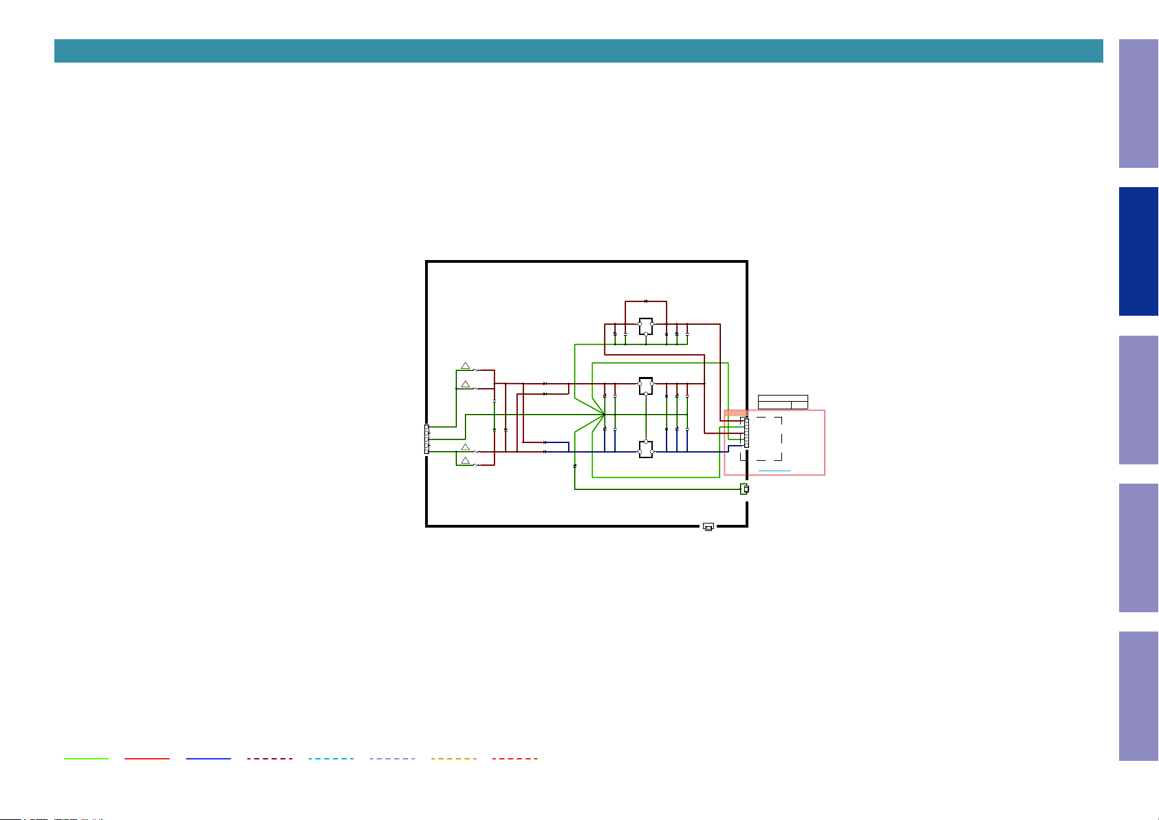
SCH09 REGULATOR
REGULATO R PART
!
F3004
T 1.25A L 250V
!
F3002
OPEN
C3004
CN302
1.AC _S2
FRO M TR ANS
3.RT N_GND
5.AC _S2
2.NC
4.NC
5 4 3 2 1
!
F3001
OPEN
!
F3003
T 1.25A L 250V
C3003
This Unit
Before Servicing
Electrical Mechanical Repair Information Updating
D3101
OPEN
IC305
CVIKI A7805BPI
IN
OUT
123
GND
OPEN
OPEN
C3002
C3001
IC301
CVIKI A7812BPI
IN
D3001 U F4007G
D3002 U F4007G
OPEN
OPEN
C3005
0.1uF (M)
D3003 U F4007G
D3004 U F4007G
C3006
C3007
OPEN
C3024
OUT
123
GND
OPEN
C3010
25V/6800uF
OPEN
C3011
25V/3300uF
GND
IN
OUT
213
IC302
HVIK IA7912PI
OPEN
OPEN
C3009
D3108
C3008
35V/470uF
*O PT ION
5.D A+5V
4.RE T_GND
3.+ 12V
2.RL Y_GND
1 2 3 4 5
1.-12V
BN301
BK301
CMD1 A569
BRAC KET
BN301
AVRS 570BT/ X580BT
TO CN771
Bra cke t
130mm
TO DIGI TAL B 'D
2mm 5 PIN W IRE
INP UT/V OLU ME PA RT
OPEN
C3012
C3014
D3103
35V/470uF
1SS133MT
BN301
OPEN
C3013
C3015
D3104
35V/470uF
1SS133MT
GND LINE
POWER+ LINE
POWER- LINE
ANALOG AUDIO
DIGITAL AUDIO
TMDS SIGNAL
ANALOG VIDEO
STBY POWER
17
BK303
CMD1 A387
BRAC KET
Page 18
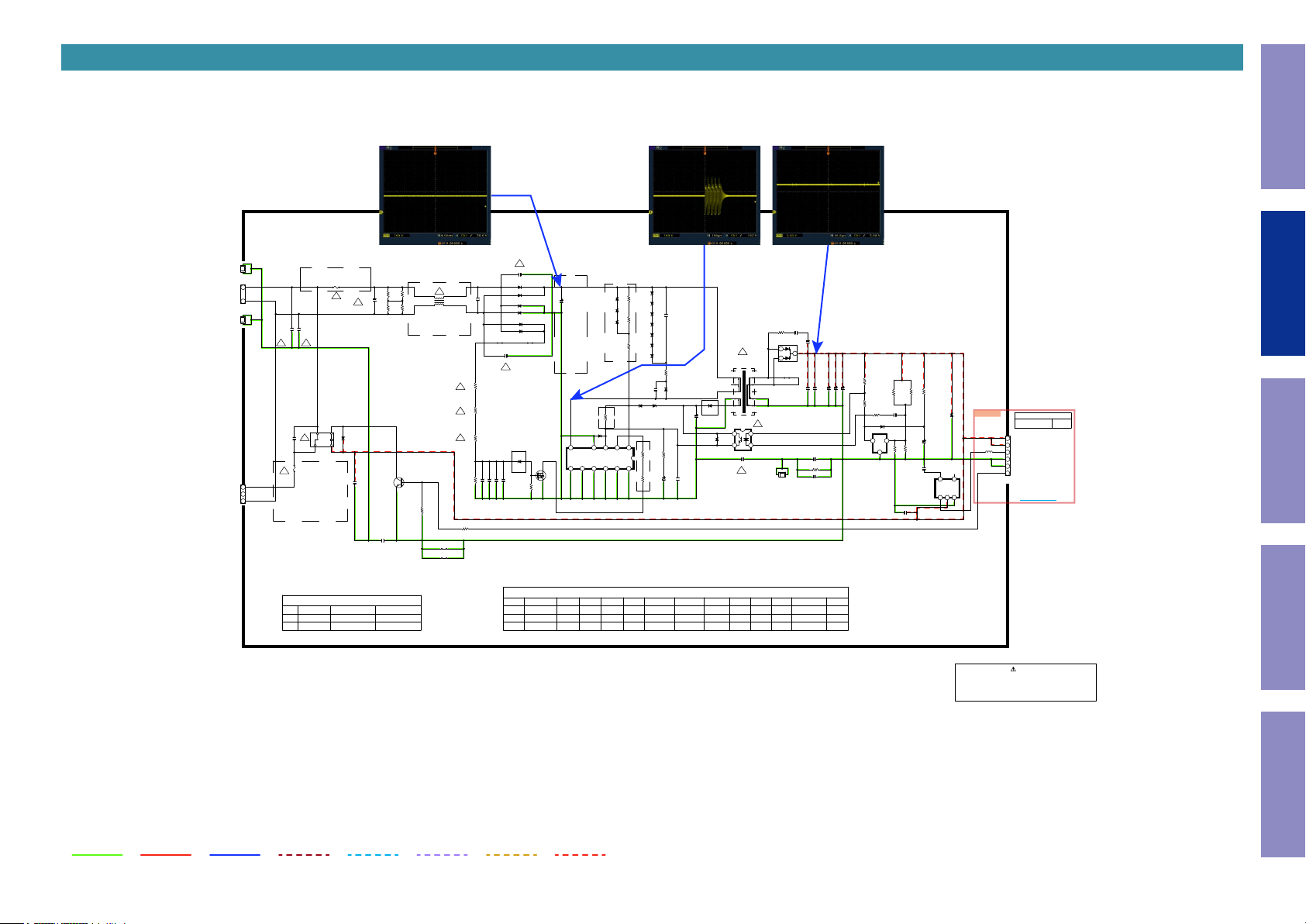
SCH10 SMPS
This Unit
Before Servicing
SMPS PA RT
OP TIO N
BK602
BRAC KET
CMD1 A834
1
2
CN601
CA3963-WV 03-2A
BK601
BRAC KET
CMD1 A834
AC100~ 120V T 2A L 250V
AC220~ 230V T 1.6A L 250V
F6001
!
!
CX601
275VAC/0 .1uF
CY602
CY601
400V/470pF
400V/470pF
!!
*O PT ION
!
8.2M
8.2M
R6029
R6027
8.2M
8.2M
LF602
R6030
R6028
E3,K :LF-4 ZB-E273H
E2,E 1C:L F-4ZB -E503H
!
!
142
!
C6001
!
CN602
YW396-NNB
AVR -S570BT/ X580BT
2 1
AC100~ 120V T 5A L 250V
TO POW ER T RANS
AC220~ 230V T 2.5A L 250V
*O PT ION
Ver
K/E3
E1C/ E2
250V/0.01u F
HF36FD /5-H LT
F6002
OP TIO N
AC100~ 120V
AC220~ 230V
3
RY601
AC
D6009
1SS133MT
0.1uF
C6021
AVRS 570BT/ X580BT
F6001 F6002
2A L 250V
1.6A L 250V
Q6003
KTC3875S YRTK
C6022
OPEN
5A L 250V
2.5A L 250V
!
R6024
10K(1608)
R6025
1.5K( 1608)
J6014
OPEN
J6015
OPEN
!
C6002 250V/0.01uF
D6001 1N 4007
D6002 1N 4007
OPEN
D6003 1N 4007
CX602
D6004 1N 4007
D6005 1N 4007
D6006 1N 4007
J6002
JUMPE R
C6003
250V/0.01u F
!
R6031
1M(2125)
R6032
1M(2125)
R6033
1M(2125)
*O PTIO N
OPEN
0.22uF
C6009
C6005
C6006 O PEN
C6007 50V/0.1u F
R6004 330K
*O PT ION
Ver
E1C/ E2
*O PT ION
*O PT ION
Z22V
ZD611
Z39V
R6008
C6004
200V/100uF
J6003
JUMPE R
Q6002
ZD621
2N7002KA
Z7.5V
D
G
S
R6006
1M(1608)
ZD621
AC
E3
K
AC120V
AC220~ 230V
AC100V
ZJ7.5 B
ZJ16B
ZJ5.6 B
ZD608
Z22V
2.2M( 0.2W )
ZD612
W)
Z39V
ZD609
Z22V
ZD613
C6011
R6009
Z39V
ZD610
Z22V
2.2M( 0.2
ZD614
1KV/ 1000pF (S MD)
Z22V
ZD615
Z22V
ZD616
R6010
1M(0 .2W)
Z22V
D6007
1N4007
270K
R6012
12346
VXC
11
12
10
AVR S570BT/ X580BT OPT ION L IST
ZJ39B
ZJ39B
ZJ39B
ZJ39B
ZD617
R6011
10(1608)
C6026
D6012
1N4007
1KV/ 47pF
ZD618
Z27V
R6015
R6013
6.8(0 .2W)
22K(1608)
*O PTIO N
C6013
C6012
R6014
1K(1608)
47/25V(NX A)
R6008 R6009 R6010 R6012
2M2 (0.2W )
2M2 (0.2W )
2M2 (0.2W )
2M2 (0.2W )
E3, K:100UF /200V
E1C ,E2 : 100UF/400V
*O PT ION
ZD601
Z12V
F
D
IC601
CVITO P268VG
S
S S S S S
7
9
8
ZD608 ZD609 ZD 610
ZJ39B
OPE N OP EN O PEN OPEN OPEN OPEN
ZJ39B
C6027
R6034
OPEN
OPEN
OPEN
C6028
1
!
T6001
VLT9 Z132ZW
1
2
3
4
5
D6008
6
UF4007G
7
C6008
0.1uF (1608)
IC602
EL817B
50V/10UF( NXA )
43
Z39V
ZD620
C6023
400V/2200pF
!
270K
1M( 0.2W )
56K
270K
1M( 0.2W )
14
13
12
11
10
9
8
!
1
2
R6013 R 6014
22K
22K
22K
3
D6013
RBQ30T 65A
BK603
CMD1A629
BRACKE T
1K
3
K
1K
J6001
OPEN
2
0.047uF( 1608)
C6014
C6024
0.047uF(1608)
R6026
OPEN( 1608)
C6025 OPEN (1608)
C6004
100UF/200V
100UF/400V
100UF/200V
OPEN
4.7uF (1608)
C6015
R6016
56(0.2W )
R6020
R6021
R6017
5.6K( 0.2W ) C6020
3.3K( 0.2W )
D6010 OPEN
R6018
0.1uF (1608)
IC603 K IA2431AP
123
REF
CATHO DE
ANODE
R6019
R6023
0.1uF (1608)
22K/F(1608)
OPEN
6.8K/ F
R6022
CVIPS T8448NR_ A
C6029
OPEN( 1608)
OPEN( 0.2W )
Z6.8V
ZD619
OPEN
C6010
C6030
15N(1608)
5
4
NC
CD
IC604
VDD
OUT
GND
2
3
1
** IMPO RTAN T SA FETY NOT ICE.
** THE UNIT OF RE SIST ANCE IS OH M.
** THE UNIT OF C APAC ITAN CE IS MICRO FARA D(u F)
** THIS SCH EMATIC DIAG RAM MAY M ODIF IED A T AN Y TI ME W ITH T HE
BN601
L6001
0
COMP ONEN T ID ENTIF IED B Y MARK HAV E SPE CIAL CHAR ACT ERISIC S.
IMPOR TANT FOR SAFE TY. WHE N REP LACING ANY OF TH ESE COMP ONEN TS
USE O NLY MANUFA CTUR ER'S S PECI FIED P ART S.
K = 1000 O HM. M = 1000KOH M.
-6
pF = 10 uF
IMPRO VEME NT O F PER FORMANC E.
BN601
AVRS 570BT/ X580BT
1
D5.2 V
D5.2 V
M_RES ET
4 3 2
DGND
DGND
6 5
MAINPOW ER
TO CN751
BN601
TO DIGI TAL B 'D
DIG ITAL POW ER P ART
220mm
C6017
C6019 5600uF/6.3V (NX A)
C6018 5600uF/6.3V (NX A)
LF602
E273H
503H
E273H
Electrical Mechanical Repair Information Updating
GND LINE
POWER+ LINE
POWER- LINE
ANALOG AUDIO
DIGITAL AUDIO
TMDS SIGNAL
ANALOG VIDEO
STBY POWER
18
Page 19

PRINTED CIRCUIT BOARDS
DIGITAL
Lead-free Solder
When soldering, use the Lead-free Solder (Sn-Ag-Cu).
DIGITAL (A side) DIGITAL (B side)
H1_CK
H1_DA
H1_5V
R7951
R7999
JK795
D7955D7953
R7956
D7956D7954
HS4
R7955
L7954
L7953
L7952
L7951
D7957
D7952
R7952
C7917
C7916
C7915
R7953
VDD09STB
VDD09EA
AVDD18EA
AVDD18TX
AVDD09TX
AVDD18RX
PVDD18
VDD18
AVDD33RX
R7996
HS1
R7722
R7778
C7550
51
R7776
5.DA+5V
R7775
4.RET_GND
3.+12V
R7777
2.RLY_GND
R7148
1.-12V
R7147
R7145
Q7110
R7166
R7196
CN771
6.MAIN_POWER
5.DGND
4.DGND
3.M_RESET
2.D5.2V
1.D5.2V
CN751
Q7108
R7168
C7133
Q7109
L7584
C7589
R7589
C7588
C7587
1 6
L7581
L7582
L7583
C7586
C7585
C7582
C7583
Pb
C7584
VERSION
+5V_4
HPD4
C7564
JK794
D7951
X7201
H1_HP
R7954
VDD09
C7993
C7992
R7992
R7991
ACABAA
YWVUTRPNMLKJHGFEDCB
A
TH791
R7907
TX_TEMP
R7906
R7905
R7908
AVDD09RX
Q7572
Q7571
C7514
R7515
C7518
L7511
C7515
R7516
C7516
L7512
R7514
C7513
C7512
R7517
IC751
L7514
L7513
C7511
C7517
R7512
R7513
D7102
R7511
C7519
C7521
C7520
C7640
T7106
R7180
R7181
R7182
C7740
C7741
ET761
MP_CUP13305Z_A
C7733
C7732
C7743
C7641
C7742
JK793
IC791
1
2
3
5
64
7
8
9
10
11
12
13
14
15
16
17
18
19
20
21 23
22
C7577
6
2
L7515
R7186
C7136
R7187
R7185
R7184
T7105
Q7111
Q7112
Q7113
R7183
BAR CODE LABEL
CN721
R7127
R7179
R7178
C7135
+5V_3
D7932
C7913
R7936
C7552
TX_HINT
TX_RST
R7134
C7113
R7133
R7132
7
R7131
5
T7104
T7103
T7102
T7109
T7125
10873
C7116
5 8
4
IC712
CK_3
DA_3
HPD3
JK792 JK791
Q7931
R7998
HS3
R7935
Q7932
D7934
R7933
R7938
R7937
R7934
D7933
D7931
R7932
R7931
HS2
R7997
T7124
T7123
RN712
C7111
R7176
R7175
R7174
R7173
7237
109 144
IC711
C7117
T7108
R7170
R7137
R7129
256
R7152
CN714
7
R7138
RN711
T7126
R7139
298
DA_2 CK_2
HPD2
+5V_2
C7912
D7924
R7926
R7923
R7928
R7925
R7927
R7924
D7923
D7921
D7922
TX_HAINT
Q7902
R7902
R7901
R7224
R7227
R7226
R7237
R7229
Q7564
Q7563
R7562
C7574
R7561
C7110
Q7562
Q7586
Q7585
C7104
36
R7108
C7103
R7107
X7111
T7120
T7101
T7119
T7118
R7101
R7103
R7102
C7119
D7101
R7104
CN715
5
FCT1AI SMT MI ICTRPFCT2
R7913
D7914
R7918
CK_1
R7917
D7913
DA_1
R7914
C7823
D7911
19 19 19 19 19
D7912
JK782
+5V_1
C7911
HPD1
R7916
R7912
R7911
R7821
R7915
Q7912 Q7911
BN791
Q7901
R7225
R7223
R7222
R7211
C7429
Q7561
C7575
C7430
25
C7433 C7432 C7431
Q7581
R7582
R7581
C7158
Q7582
C7824
R7824
L7404
C7468
C7470
C7469
C7568
C7569
C7471
R7471
C7446
C7567
R7554
C7566
R7472
R7475
L7552
R7476
R7448
R7447
Q7552
C7444
R7552
C7565
R7551
L7551
C7427
Q7551
R7417
6439
IC743
RN749
50
RN748
RN751
RN750
R7418
R7430
C7434
R7419
RN745 RN744
10265
26
RN746
RN747
L7585
L7104
L7103
C7122
L7105
L7108
L7107
L7106
C7123
L7102
L7101
21
C7578
26
C7579
21.FL_CLK
27.NC
26.DGND
20.FL_CE
22.FL_DATA
23.CPU_POWER
24.MCU+5V
25.MCU_3V3
R7416
19.FL_RST
JK783
C7832
C7822
R7833
C7833
JK784
Q7612
Q7613
C7645
R7834
R7650
R7649
Q7614
D7606
R7646
R7669
C7632
C7707
D7605
D7609
D7607
R7757
L7403
C7454
R7758
C7459
R7484
C7467
C7465
C7463
C7461
C7458
4833
6449
R7479
R7477
R7411
RN743
R7410
R7413
R7422
C7424
L7113
L7112
L7111
L7110
L7109
C7709
IC744
3217
T7404
T7403
T7401
T7402
16
C7450
C7451
R7478
C7449
C7448
C7125
C7120
R7409
R7407
R7480
IC741
C7442
38
C7443
L7401
C7505
C7506
C7504
C7404
R7593
L752
C7503
R7403
C7403
C7405
X741
R7402
C7581
Q7592
RN742
RN741
L7402
R7425
128103
C7423
Q7591
R7424
R7423
L7123
L7122
L7119
L7130
L7126
L7125
L7124
L7120
L7117
L7116
L7115
L7114
11
1 27
L7127
CN711
220 10
R7759
R7760
R7766
R7767
1.ISEL_A
6.-12V
5.+12V
7.MIC_SIGNAL
8.MIC_GND
3.MIC_DET
4.POWER_KEY
9.NC
2.ISEL_B
11.VSEL_A
10.H/P_DET
12.VSEL_B
13.KEY_3
14.KEY_2
15.KEY_1
16.RED_LED
17.GRN_LED
18.RC_IN
1
R7664
1
2
D7604
D7603
R7765
R7764
C7702
D7841
C7706
C7617
C7453
C7121
JK772
2 4
5
C7638
C7703
Q7610
C7642
R7652
C7841
R7841
R7648
R7645
R7641
R7647
C7615
C7644
IC766
85
C7705
R7743
Q7611
R7643
C7629
R7745
R7748
C7712
R7753
R7756
C7580
T7609
C7643
R7644
R7742
R7741
R7732
4
85
R7728
C7627
R7730
R7727
R7729
C7663
4
IC767
R7679
C7658
R7678
R7726
C7661
R7670
C7660
R7671
4
R7676
C7664
C7652
C7656
C7665
C7653
R7725
C7680
85
R7677
C7662
C7657
R7681
R7672
R7680
R7673
R7695
C7678
C7659
C7676
C7674
R7686
4
R7692
C7681
C7668
R7719
R7694
R7687
C7672
C7682
C7669
R7718
IC763 IC762
85
R7693
C7696
C7679C7673
R7688
R7697
R7696
C7693
R7689
C7675
R7711
C7691
R7702
4
C7694
R7708
C7697
R7710
R7724
R7703
C7689
C7690
C7698
C7686 C7685
IC764
R7723
Q7609
Q7608
R7709
85
R7704
C7141
R7712
R7705
C7692
C7695
R7713
R7592
R7591
C7142
C7802
C7803
C7510
C7509
C7508
ET751
T7605
T7604
T7603
T7608
T7607
T7606
T7601
CN772
C7714
T7602
131 7
1.FL
6.AGND
9.FR
7.SR
8.AGND
2.AGND
4.AGND
5.CEN
3.SL
10.+12V
12.MUTE_+B
13.DGND
11.RLY_GND
3
41 63
R7660
C7761
R7642
R7623
C7639
R7621
C7764
C7763
R7625
85
R7628
IC769 IC768
C7768
C7767
R7629
R7630
C7666
R7682
IC770
R7684
R7685
R7698 R7683
C7683 C7667
R7700
Q7605 Q7604
R7701
C7684
R7699
R7714
C7699
C7631
R7716
Q7606
R7717
R7715
C7700
C7717
C7716
R7735
R7734
C7801
C7598
C7597
C7596
C7599
R7624
R7615
R7626
4
R7627
R7619
16
IC771
16
17 32
D7602
C7595
C7594
C7593
T7112
T7110
2.H/P_RLY
1.HI-B_RLY
C7762
R7622
85
R7618
C7758C7757
R7620
SW
R7737 R7736
10.USB_DAC_MUTE
C7795
CN712
51 11
T7111
T7114
3.FRONT_RLY
4.C/S_RLY
5.NC
2 57
R7613
11.USB_EN
9.BX_RST/BT_RST
8.BT_RX
7.BT_TX
6.USB_POWER1
5.USB3V3
4.DGND
3.DGND
2.D5V
1.D5V
6.DC_PROT
R7655
R7738
R7659
R7658
TU771
1.CH_GND
JK771
2.INT
3./RST
R7654
4./CE
R7637
R7740
R7614
C7611
5.SDIO
C7612
6.SCLK
R7651
7.VCC
C7751
R7612
R7611
C7752
R7653
8.R-OUT
C7610
9.L-OUT
C7613
TU771
R7656
1 9
C7754C7753
R7616
4
4
6
R7657
C7614
R7617
L7601
C7605
C7622
C7739
R7721
C7607
C7769
C7721
R7604
C7720
R7606
R7602
R7601
R7720
R7603
R7605
3217
C7770
C7774
5.USB/BT_L
4.DA_GND
3.USB/BT_R
2.DA_GND
1.+5VA
C7773
C7777
R7774
51
R7773
C7630
C7501
C7502
CN752
C7794
C7713
C7152
D7601
C7155
T7132
T7131
C7790
C7789
C7157
51 11
C7154
C7156
C7153
CN713
T7116
T7113
T7117
T7115
8.NC
9.ASO_DET
10.THERMALDET_A
11.THERMALDET_B
7.+/-B DETECT
25 7
3
1
6 34 1
C7621
1
4
6
9
R7771
R7772
C7124
C7144
15
C7618
C7143
4
C7765
C7755
C7766
C7756
C7772
C7771
R7662
R7661
C7775
R7640
R7639
C7776
1511
1511
1
R7922
2
2
C7793
5
C7704
R7744
R7746
R7747
C7708
C7710
R7752
R7754
R7755
C7654
R7674
C7655
R7675
R7690
C7670
C7671
R7691
R7706
C7687
C7688
R7707
C7127
C7126
D7608
C7792
C7791
C7476
C7466
C7464
C7462
C7460
C7473
C7711
C7474
R7412
C7456
C7480
C7479
C7457
R7481
R7482
C7455
R7473
R7474
C7477
C7727
C7452
C7478
R7483
C7475
C7728
C7447
C7445
C7736
R7406
R7405
C7737
C7409
C7406
C7408
C7407
C7738
C7149
R7404
C7402C7401
C7425
R7420
C7426
11
113 7
C7437
169
IC745
C7555
R7553
R7415
R7414
R7408
C7415C7414C7412C7410
R7431
R7443
R7427
R7445
R7428
R7426
R7444
C7436C7435
4
R7432
R7446
S570BT E3
IC742
X580BT E2
X580BT K
C7419 C7418 C7417 C7416
5 8
X580BT E1C
C7422
C7420
R7401
C7428
R7429
27
21 1
262
2010
R7921
Q7922 Q7921
R7904
R7903
R7239
C7211
C7213
C7212
R7228
C7215
R7449
85
IC725
9 16
IC723
IC722 IC721
8
8
4
C7214
R7234
R7233
R7235
R7231
R7232
R7230
R7568
D7563
D7562
R7583
Version Option Res
VER.
R7113
R7114
10K
4K7
10K
OPEN
10K
OPEN
10K
10K
C7553
C7554
C7556
C7563
L7542
C7557
R7545
L7541
R7549
R7546
R7544
C7551
R7542
R7543
R7541
R7238
C7217
13 241213 24
12
HDMI_SPDIF
RN721
RN723 RN722
C7216
R7236
HDMI_MCK
HDMI_DATA1
HDMI_DATA0
HDMI_BCK
HDMI_LRCK
HDMI_DATA2
HDMI_DATA3
R7560
R7569
R7585
R7584
R7195
R7113
R7192
R7159
R7114
C7106
R7162
C7105
R7151
R7150
C7108
C7107
R7149
C7109
Q7593
R7193
R7194
R7565
R7567
C7102
C7592
D7592
R7165
C7101
C7129
R7564
C7591
C7590
R7563
R7598
D7591
R7141
C7118
R7142
R7566
R7547
R7548
L7543
R7983
IC754
R7984
R7985
R7986
C7560
C7559
C7558
R7975
R7540
C7507
R7978
R7968
R7977
R7980
R7979
R7982
R7981
R7976
C7921
C7922
L7921
C7112
R7163
C7131C7130
R7164
Q7107
C7114
R7161
Q7106
R7158
C7115
C7146
R7156
R7136
Q7105
R7188
R7144
R7143
R7140
R7154
R7153
R7155
C7128
C7927
C7925
Q7942 Q7941
C7975
R7969
C7961
C7134
D7943
R7944
R7943
D7944
R7947
D7941
C7562
C7561
L7931
C7946
C7966
C7972
C7970
C7969
C7945
C7944
C7576
R7572
R7571
DA_4
C7914
D7942
R7946
R7948
R7945
CK_4
R7941
R7942
R7972
R7974
R7973
C7996
C7995
C7994
R7966
R7964
R7990
R7970
R7989
R7971
R7988
R7987
R7962
R7963
R7961
C7983
C7982
R7965
C7981
C7985
C7980
C7951
C7984
C7979
C7959
C7939
C7968
C7949
C7931
C7955C7954
C7976
C7929
C7957 C7956
C7978
C7935
C7940
C7971
C7932
C7958
C7977
C7936
C7934
C7947
C7974
C7965
C7967
C7930
C7963
C7964
C7973
C7923
R7967
C7960
C7926
C7924
C7962
C7536
C7535
R7527
L7525
L7524
C7526
C7525
L7523
C7534
L7522
L7521
IC752
C7529
C7528
C7527
C7531
R7525
R7521
R7523
R7522
R7526
C7524
R7524
C7523
C7522
R7501
T761
R7502
R7503
C7570
R7505
R7504
IC761
R7506
R7507
C7572
D7561
C7573
C7571
C7948
L7927
C7950
L7928
C7928
L7922
C7937
L7925
C7938
C7952
L7929
C7953
C7942
L7926
C7943
C7941
C7933
L7924
L7923
L7930
C7549
R7539
R7538
R7537
C7547
C7533
C7548
C7532
C7538
C7546
C7545
L7533
C7544
L7532
L7531
IC753
C7541
C7540
C7539
C7542
15
R7530
C7530
R7531
C7543
R7535
R7533
R7532
C7537
R7536
R7534
C7132
R7167
6 1
This Unit
Before Servicing
Electrical Mechanical Repair Information Updating
19
Page 20
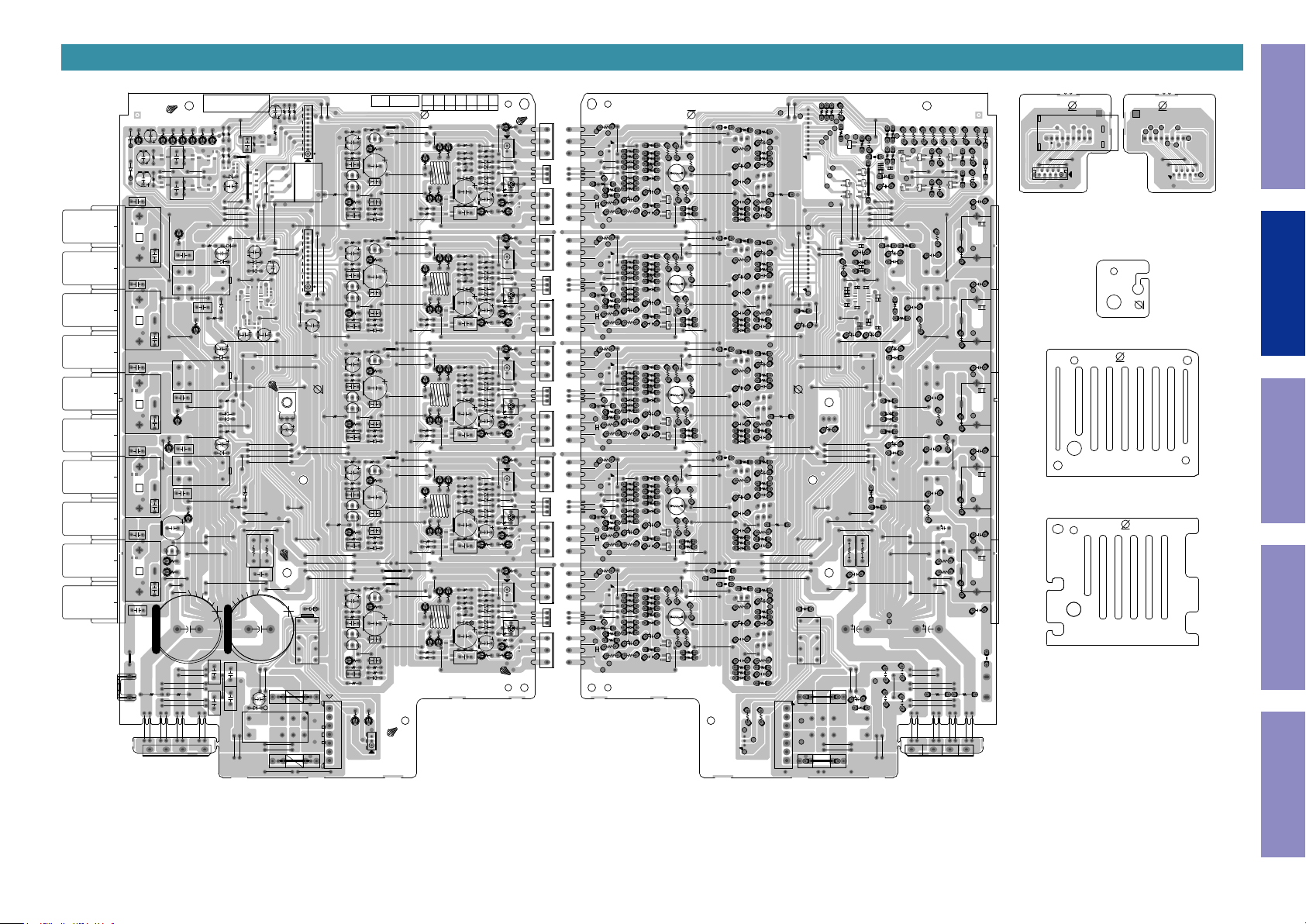
MAIN, TUNER, PHONE WIRE GUIDE, FRONT CABLE GUIDE, USB WIRE GUIDE
J5933
MAIN (A side) TUNER (A side)
C5716
R5713
R5712
R5711
BAR CODE
R5720
R5719
R5718
R5717
R5716
R5715
R5714
D5703
C5717
R5707
C5712C5710
C5713
R5708
J5671
D5704
C5711
1
2
1
2
1
2
C5610
1
2
C5609
1
2
J5601
BK051
J5628
CMD1A569-V1
D5701
R5705
R5706
C5606
JK502
J5944
3
R5722
FR
C5608
5 4
2 3
C5605
RY562
J5122
J5121
JK501
C5718
3
R5721
C5607
J5123
FL
5 4
C5611
2 3
RY564RY563
JK503
3
R5725
CEN
C5614
R5724
J5945
5 4
2 3
JK505
3
C5613
SR
C5708
SL
Q5702
BE
R5704
JK504
R5703
3
C5612
J5644
C5615
C5706
R5710
J5632
J5633
J5631
J5630
J5629
~~
-
J5910
C5701
R5701
R5818
R5817
R5729
J5672
J5670
R5813
C5601
C5719
D5602
6
1
D5808
R5812
C5603
D5604
6
1
C5722
J5932
J5653
C5602
D5603
C5721
6
1
C5720
J5626
R5814
R5723
J5649
J5650
J5646
J5645
J5643
C5714
J5641
J5640
J5639
J5642
J5638
R5709
J5637
J5636
J5634
J5635
D5701
C5715
+
R5819
J5821
D5807
J5822
C5807
J5908
J5668
J5667
J5666
J5665
D5809
J5660
C5819
D5815
D5816
J5942
C5825
J5120
J5651
J5659
R5816
D5812
D5811
J5652
R5815
J5648
D5810
R5827
R5826
J5647
C5702
C5801
C5703
D5806
41
5
RY586
J5901
J5902
R5702
AVR-S600 Series
11.THERMALDET_B
10.THERMALDET_A
9.ASO_DET
8.CURRENT_DET
7.-12V
6.DC_PROT
5.AMPSIG_DET
4.C/S_RLY
3.FRONT_RLY
2.H/P_RLY
1.HI-B_RLY
J5911
J5625
J5907
BN501
J5673
J5624
13.DGND
12.MUTE_+B
11.RLY_GND
10.+12V
9.FR
8.AGND
J5943
7.SR
6.AGND
C5820
5.CEN
4.AGND
3.SL
2.AGND
1.FL
J5941
J5623
C5826
C5723
J5622
J5119
J5621
ET501
C5707
J5620
J5619
J5618
J5617
J5616
J5655
J5611
J5654
C5828
J5674
C5704
1
432
J5903
J5904
F5801
T5A L 250V
J5804
8
J5906
J5905
F5802
J5805
J5934
7 11
J5935
BN502
11.THERMALDET_B
10.THERMALDET_A
9.ASO_DET
8.NC
7.B_DETECT
6.DC_PROT
5.NC
4.C/S_RLY
3.FRONT_RLY
2.H/P_RLY
1.HI-B_RLY
AVR-S500 Series
137
J5613
R5403
Pb
CUP13307Z-1 MAIN PART
J5610
D5601
5678
RY560
1.AC_L
2.NC
3.AC_H
4.CEN
5.AC_H
6.NC
7.AC_L
T5A L 250V
J5615
R5501
C5501
R5502
R5504
C5502
Q5501
Q5502
R5503
R5506
R5507
C5504
J5517
R5401
C5401
R5402
R5404
C5402
Q5401
J5614
Q5402
J5419
R5406
R5407
C5404
J5417
R5301
C5301
R5302
R5304
C5302
Q5301
Q5302
R5303
R5306
R5307
C5304
J5317
J5612
R5201
C5201
R5202
R5204
C5202
Q5201
Q5202
R5203
R5206
R5207
C5204
J5609
J5608J5605
J5607
J5603
R5101
C5101
R5102
R5104
C5102
Q5101
Q5102
R5106
R5107
C5104
R5103
R5726
CN503
IN
BE
BE
BE
BE
BE
BE
BE
BE
BE
BE
J5518
J5418
J5318
J5218
J5118
R5505
C5503
R5405
C5403
R5305
C5303
R5205
C5203
C5206
R5209
R5208
D5201
R5105
R5727
1.HP_RCH
BE
C5506
R5509
R5508
D5501
BE
C5406
R5409
R5408
D5401
BE
C5306
R5309
R5308
D5301
BE
BE
C5106
R5109
R5108
D5101
3.HP_LCH
2.AGND
BN505
VERSION
FCT1 FCT2RPICTMISMTAI
Pb
J5515
J5501
J5514
J5509J5409J5309J5209
J5513
Q5503Q5403Q5303Q5203Q5103
R5510R5410R5310R5210R5110
FR
C5505C5405
R5532
J5512
J5511
R5521
R5519
R5530
R5529
J5510
J5508J5408J5308
J5416
J5415
J5401
J5414
J5413
SRSLFL
R5432
J5412
J5411
R5421
R5419
R5430
R5429
J5410
J5316
J5315
J5301
J5314
J5313
CEN
C5305
R5332R5232R5132
J5312
J5311
R5321
R5319
R5330
R5329
J5310
J5216
J5201
J5215
J5214
J5213
C5205C5105
J5212
J5211
R5221
R5219
R5230
R5229
J5210
J5208
J5116
J5115
J5604
J5602
R5122
J5101
J5109
J5114
J5113
J5112
R5121
R5119
C5103
J5111
R5130
R5129
J5108
CUP13307Z-1 MP 2022.05.06
R5522
R5520
L5501
J5507
R5531
R5514
R5511
R5528
R5527
D5505
D5504
R5525
R5524
J5506
D5503
D5506
D5502
C5508
R5523
R5512
C5509
C5507
R5516
R5422
R5420
L5401
J5407
R5431
R5414
R5411
R5428
D5405
R5427
D5404
R5425
R5424
J5406
D5403
D5406
D5402
C5408
R5423
R5412
C5409
C5407
R5416
R5322
R5320
L5301
J5307
R5314
R5331
R5311
R5328
D5305
R5327
D5304
R5325
R5324
J5306
D5303
D5306
D5302
C5308
R5323
R5312
C5309
C5307
R5316
R5222
R5220
B E B E
R5518
J5505
CN550
ECCCBCBC
Q5504Q5505 Q5506
BE
J5504
J5503
J5502
VR550
R5533
R5534
R5418
R5513
R5517
B E B E
R5515
J5405
CN540
KTB2630G
Q5404Q5405 Q5406
BE
J5404
J5403
J5402
VR540
R5433
R5434
R5413
R5417
B E B E
R5415
R5318
J5305J5205
CN530
KTB2630G KTB2630GKTC3114KTC3114
KTC3114KTC3114
Q5304
BE
B E C
J5304
J5303
J5302
Q5305 Q5306
VR530
R5333
R5334
R5313
R5317
B E
R5315
R5218
CN520CN510
L5201
R5231
R5228
R5227
R5225
R5224
D5206
C5208
R5223
C5209
R5120
L5101
R5131
R5128
R5127
R5125
R5124
D5106
C5108
R5123
C5109
Q5204Q5205 Q5206
BE
B E
J5207
J5204
J5203
R5214
J5202
R5211
KTD1630G KTD1630G KTD1630G KTD1630G
D5205
VR520
D5204
R5233
J5206
R5234
R5213
D5203
R5217
D5202
R5212
C5207
R5216
J5107
R5114
R5111
D5105
D5104
J5106
D5103
D5102
R5112
C5107
R5116
B E B E
R5215
J5105
KTB2630G KTB2630G
E
KTC3114
Q5104
BE
B E E EB B
R5118
J5104
J5103
Q5105 Q5106
KTD1630G
E C B E BC E BC E BC E C E BC E BC B E BC E BC
J5102
VR510
R5133
R5134
R5113
R5117
R5115
R5126R5226R5326R5426R5526
Q5107Q5108Q5207Q5208Q5307Q5308Q5407Q5408Q5508 Q5507
TUNER (B side)MAIN (B side)
CUP13307Z-2 MP 2022.05.06
E3/K CNVYST990-A9U2
Pb
CEN
FLSLSRFR
11 7
Q5701
1
Q5601
Q5806
13
7
1
R5830
R5831
R5837
R5835
5 8
C5823
R5834
R5832
R5840
Pb
5 6 7 8
4 3 2 1
8
R5728
R5811
Q5603
R5821
R5810
C5806
Q5604
Q5705Q5708
Q5602
6
R5836
C5818
1
4
C5824
IC501
R5838
C5817
R5833
C5821
R5839
6
1
6
1
4 1
5
Q5706
Q5707 Q5704
Q5703
C5617
3
54
23
54
23
54
23
+
2
C5616
3
2
C5620
3
2
C5619
3
2
C5618
3
2
~~
-
E2 CNVYST990-D8E3
E1C CNVYST990-A2J1
TU500
J5928
9.L_OUT
8.R_OUT
1
PHONE WIRE GUIDE (A side)
1
FRONT CABLE GUIDE (A side)
1
1
1
TUNER
Pb
1 8
J5927
2198
7.VCC
6.SCLK
5.SDIO
1.CH_GND
2.INT
3./RST
4./CE
BN508
ET1
Pb
8 1
CUP13307Z-3 MP 2022.05.06
Pb
CUP13307Z-4 MP
Pb
AVR-S500 Series
USB WIRE GUIDE (A side)
Pb
CUP13307Z-5 MP
AVR-S500 Series
1
298
1.CH_GND
2.INT
This Unit
9.L_OUT
8.R_OUT
7.VCC
6.SCLK
5.SDIO
4./CE
3./RST
Before Servicing
Electrical Mechanical Repair Information Updating
20
Page 21
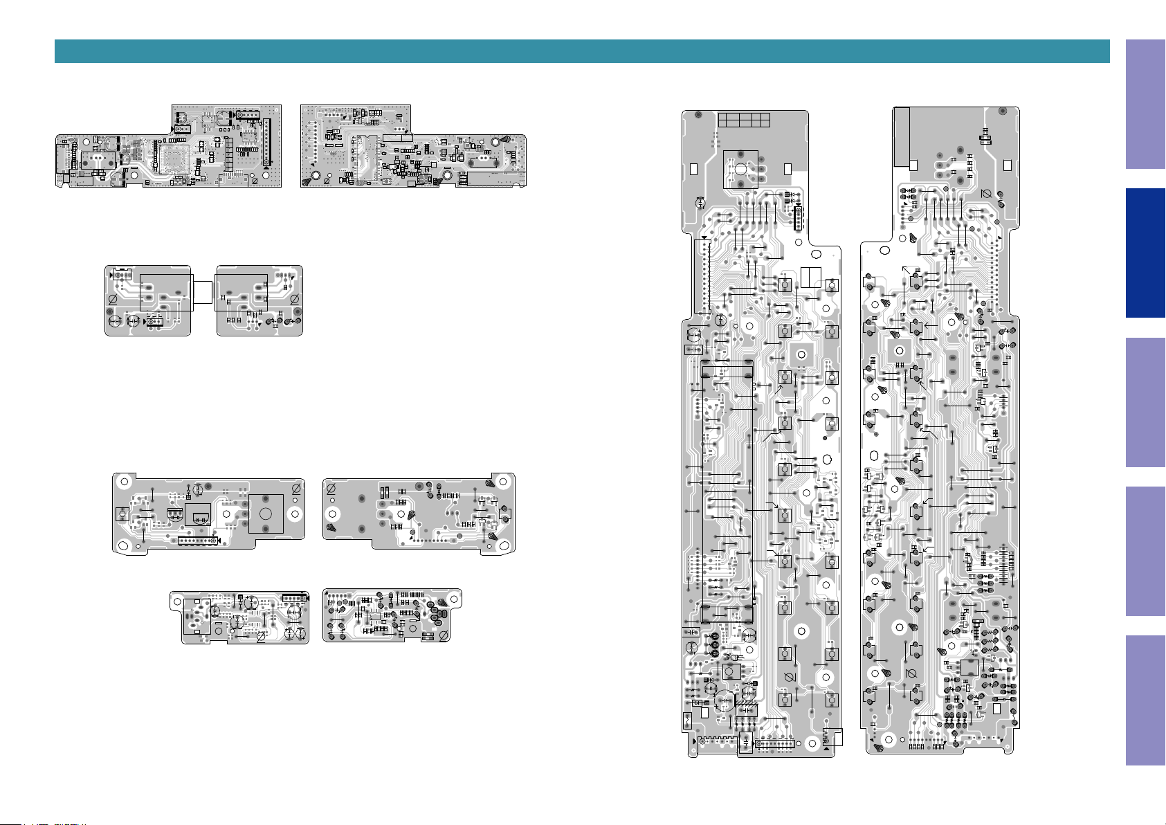
USB, FRONT, PHONE, STANDBY, MIC
5
X2001
R2009
C2038
L2004
C2019
USB (A Side)
C2111
T2002 T2003
L2008
C2121
C2122
D2003
CN213
C2046
R2071
C2051
C2109
R2082
C2110
C2054
R2070
R2067
R2068
R2069
C2044
1 2 3 4
10
L2007
C2104 C2112
D2004
L2020
R2064
D2005
C2043
6.BT_GND
1.VDD
7.RXD
2.RESET
R2066
C2124
C2123
RN2010
R2065
8.BT_GND
3.RTS
CN213
L2017
4.CTS
9.I2C_SCL
C2107
5.TXD
10.I2C_SDA
PHONE (A Side) PHONE (B Side)
C2099
JK201
C2106
C2129
2.A GND
3.H/P L
1.H/P R
PbPb
LUG13
C1067 C1065
CN104
C2035
L2012
C2034
C2065
C2057
C2096
C2083
1 171615141312111098765432
L2010
L2019
R2080
L2009
R2081
A
B
R2055
C
L2014
R2053
D
R2054
E
L2016
F
R2052
G
R2040
L2015
H
R2078
J
R2049
K
L
RN2009
M
N
P
R2093
R
T
R2094
U
T2001
C2128
C2105
CUP12957Z-4
R2056
R2057
C2037
MP STAGE
2 3
7
8
3.H/P DET
2.D GND
1.D GND
BN131
STANDBY (A Side)
J1111
POWER
SW101
R
J1113
J1112
J1114
BN101
MP_CUP13306Z_A
C2070
C2079
1
JK104
D1002
W/G
R W
AVRX1500BKE3
D1012
9
1
CUP12957Z-2
MP STAGE
C2001
CN416
R2037
R2038
R2039
IC2006
R2028
R2033
L2013
VOP12957C
3
5 8
IC2001
4
C2125
C2127
C2126
1.DEBUG_RX
3.DGND
2.DEBUG_TX
C2023
RN2002
R2036
FCT2
RN2008
RP
RN2001
RN2003
FCT1AI SMT MI ICT
RN2007
R2030
R2032
RN2004
R2031
R2029
1.VCC
R2035
2.NTRST
R2034
3.TDI
RN2005
4.TCK
5.TMS
6.TDO
7.RESET
C2003
8.DGND
9.DGND
RN2006
R2097
R2008
R2010
1
C1083
R1057
1.D GND
3.H/P DET
2.D GND
LUG14
C1429
9.POWER_KEY
7.RED_LED
8.MCU+5
MIC (A Side)
J1106
JK105
C1402
5
4
2
6
7
C2017
C2016
R2004
R2026
R2005
R2007
R2006
3.USB/BT_R
2.DA_GND
5.USB/BT_L
4.DA_GND
1.+5VA
5
BN211
C2015
C2011
C2014
R2024
R2023
10
C2039
R2089
C2041
R2022
7 11
IC2003
2011
R2016
C2004
C2005
R2018
R2015
R2017
R2019
R2020
R2060
R2063
BN212
R2059
R2061
R2062
10
CN214
Pb
23
1.H/P R
L1010
3.H/P L
2.A GND
7
L1012
8
C1424
L1013
C1069
Pb
C1072 C1071
C1084
L1011
C1068
C1066
15
11 7
L2021
IC2004
R2025
C2010
C2006
MP_CUP13306Z_A
C2040
C2042
D2008
D2001
R2021
C2009
C2008
C2007
C2027
C2025
L2006
10.USB_DAC_MUTE
5.USB3V3
4.DGND
3.DGND
2.D5V
11.USB_EN
8.MCS)RX
9.MCS_RST
7.MCS_TX
6.USB_POWER1
1.D5V
C2024
1
R2084
C2026
R2087
R2086
27
Pb
R2088
R2085
C2115
C2114
C2020
C2002
L2002
C2013
C2012
2.DEBUG_TX
3.DGND
1.DEBUG_RX
L2003
R2002
R2003
R2001
IC2005
VERSION
R2048
R2047
R2091
C2022
R2045
R2044
R2043
R2042
R2041
R2046
R2050
C2077
C2073
C2074
C2021
C2059
C2078
C2095
C2097
C2058
C2071
C2080
C2098
R2027
C2082
C2093
D2009
C2056
R2014
C2061
C2091
C2028
C2094
C2060
C2081
R2074
28 54
85
C2067
C2085
C2084
C2068
R2076
4
R2072
C2030
C2062
R2012
R2011
L2011
C2063
C2018
IC2002
L2005
C2075
C2033
4
C2069
C2064
R2073
C2117
C2055
R2090
IC2007
C2120
C2092
IC2008
C2029
C2031
C2089
C2036
C2032
C2090
C2086
R2013
R2092
C2100
C2103
C2101
C2102
C2076
C2072
R2095
R2096
C2108
C2132
C2131
C2130
D2002
D2006
D2007
C2119
C2118
85
L2018
C2116
1234
BAR CODE LABEL
C2053
C2052
C2050
C2045
R2083
C2113
C2049
STANDBY (B Side)
CUP12957Z-3
MP STAGE
A B C
2.ISEL_A
3.ISEL_B
4.DGND
5.DGND
6.GRN_LED
D1401
J1110
VR102
1.+3v3
BN12B
C1405
J1108
5.MIC DET
4.+12V
J1107
3.-12V
C1407
2.MIC SIGNAL
1.AGND
*J1108 OPTION (USE)
AVR-S640H
AVR-S740H/X1500H
C1411
Pb
Pb
PbPb
15
L1403
C1452
-12V
J1104
C1410
MIC (B Side)
R1408
R1409
C1408
R1411
R1412
IC101
+12V
85
C1417
5.MIC DET
4.+12V
3.-12V
2.MIC SIGNAL
1.AGND
R1433
R1435
R1434
R1431
R1436
C1450
R1432
C1451
D1406
1.+3v3
R1437
D1407
C1428
C1427
A
R1414
R1415
C1426
C B
R1413
R1416
C1425
19
+12V
6.GRN_LED
7.RED_LED
8.MCU+5
9.POWER_KEY
5.DGND
2.ISEL_A
3.ISEL_B
4.DGND
R1405
R1403
C1413
R1407
C1414
R1027
C1406
4
C1415
C1416
R1042
R1041
R1045
C1055
Q1009
Q1008
Q1012
+5V
C1401
R1402
L1402
L1401
R1401
R1054
5
1
3
4
2
6
7
R1404
R1406
C1404
C1403
D1404
D1405
Pb
Q1011
R1044
R1043
C1054
LUG11
1.ISEL_A
2.ISEL_B
3.MIC_DET
4.POWER_KEY
5. +12V
6. -12V
7.MIC_SIGNAL
8.A_GND
9.B/P_IRIN_DE
10.H/P_DET
11.VSEL_A
12.VSEL_B
13.KEY_3
14.KEY_2
15.KEY_1
22.FL_DATA
23.CPU_POWER
24.MCU_5V
25.MCU_3V3
26.D_GND
27.NET_FACT_RST
C1017
5
8
J1047
J1046
J1045
43
50
53
J1005
57
J1004
C1007
Q1014
Q1001
F1001
FRONT (A Side) FRONT (B Side)USB (B Side)
16.RED_LED
17.GRN_LED
18.RC_IN
19.FL_RST
20.FL_CE
21.FL_CLK
C1075
BN12B1
1 27
11
21
J1053
C1010
BK101
J1051
FL101
J1048
BK102
R1427
C1004
R1426
R1425
R1424
R1062
R1007
D1001
1.VDISP
T 200mA L 250V
1 7
MI ICT FCT1 FCT2 RP
MP STAGE
FRONT PART
CUP12957Z-1
BAR CODE
GNDGND
VR101
C1076
C1077
CUP12957Z-1/FRONT PART/MP STAGE
1. A GND
2. MIC SIGNAL
3. -12V
4. +12V
D1402
5. MIC DET
D1403
J1102
J1095
J1099
J1098
J1097
J1096
J1094
J1093
J1092
J1090
1020 2
J1088
J1089
J1084
J1083
J1082
26
C1019
J1054
J1055
J1052
J1056
J1115
J1050
J1049
J1044
J1043
J1041
J1040
J1039
J1038
J1033
R1067
R1030
R1423
J1009
J1064
D1005
C1006
2.NC
3.GND
4.NC
5.FL AC
6.NC
J1075
J1057
J1058
J1060
J1059J1042
S640H : INFO
S540BT : MODE
S740H : BAND
X250BT/X550BT/X1500H : Q/S_1
S640H: BAND
S540BT/S740H: TUNE-
J1037
J1036
J1034
J1035
S540BT/S740H : PRESET+
X250BT/X550BT/S640H : TUNE+
J1032
J1007
J1006
J1015
J1008
C1038
J1010
LD101
RC101
D1003
C1005
C1003
C1002
J1001
R1002
R1001
CN102
7.FL AC
C1001
J1100
J1087
J1086
J1085
X250BT/X550BT/X1500H : DIMMER
J1031
J1081
X1500H : ZONE2 SEL
S540BT : SOUND
S540BT : SOUND
R1003
J1077
S540BT/S640H : SLEEP
S540BT/S740H: TUNE+
R1004
J1101
J1091
J1078
X250BT/X550BT/X1500H : Q/S_3
S540BT/S640H/S740H : DIMMER
J1076
S740H : MODE
X250BT/X550BT/X1500H : Q/S_2
S640H: MODE
X250BT/X550BT/X1500H : STATUS
J1062
J1029
J1109
S540BT/S740H : PRESET-
X250BT/X550BT/S640H: TUNE-
S740H : ZONE2 SEL
X250BT/X550BT: PRESET+
S740H : ZONE2 ON/OFF
X250BT/X550BT: PRESET-
J1002
J1079
SW110
J1061
J1063
SW116
SW109
X1500H : ZONE2 ON/OFF
S640H/X1500H: PRESET- S640H/X1500H: PRESET+
BN12A
5
S640H/S740H : PURE
X250BT/X550BT/X1500H : Q/S_4
SW118
SW117
SW104
S540BT : ADJUST
VERSION
SW102
J1074
J1080
J1073
S540BT : ADJUST
S640H/S740H : GAME
J1072
J1071
J1070
J1068
J1066
J1065
SW103
SW114
SW108
S640H/S740H : MUSIC
S540BT : BASS/TREBLE
S640H/S740H : MUSIC
S540BT : BASS/TREBLE
S640H/S740H : MOVIE
S540BT : ON/OFF
S540BT : ON/OFF
S640H/S740H : MOVIE
BN10
J1027
J1026
J1025
J1020
J1022
J1021
J1019
J1018
R1092
Q1023
Q1022
Q1017
J1023
R1091
J1024
Q1018
SW111
S540BT/S640H/S740H : ADJUST
J1067
J1028
J1103
J1017
J1014
S540BT/S640H/S740H : Q/S_4
J1016
J1069
J1013
SW105
S540BT/S640H/S740H : Q/S_3
J1030
S540BT/S640H/S740H : Q/S_2
J1012
SW115
PbPb
J1011
J1003
SW106
S540BT/S640H/S740H : Q/S_1
2.ISEL_A
3.ISEL_B
1.+3v3
4.DGND
5.DGND
6.GRN_LED
7.RED_LED
8.MCU+5
9.POWER_KEY
31
BN101_1
9
R1085
SW119
R1080
SW113 SW112
SW107
3.H/P DET
2.D GND
1.D GND
2.D GND
3.H/P DET
CN103
1.A GND
2.MIC SIGNAL
3.-12V
4.+12V
-12V
5.MIC DET
C1409
15
R1410
+12V
S540BT : ADJUST
S640H/S740H : PURE
S540BT/S640H/S740H : ADJUST
X250BT/X550BT/X1500H : Q/S_4
C1082
R1046
R1078
X250BT/X550BT/X1500H : Q/S_3
R1084
R1071
S540BT : ADJUST
S640H/S740H : GAME
R1082
R1081
R1087
R1086
R1076
Q1024
S540BT/S640H/S740H : DIMMER
Cushion
X250BT/X550BT/X1500H : Q/S_2
S540BT/S640H : SLEEP
S740H : MODE
R1083
S540BT : MODE
S640H : INFO
S740H : BAND
X250BT/X550BT/X1500H : Q/S_1
S540BT/S740H : TUNE+
X250BT/X550BT/X1500H : STATUS
S640H : MODE
R1072
GND
X250BT/X550BT/X1500H : DIMMER
S540BT/S740H : TUNE-
S640H : BAND
Q1021
Q1020
Q1019
R1090
R1079
/S740H : Q/S_4
S540BT/S640H
S540BT/S640H/S740H : Q/S_3
GNDGND
S540BT/S640H/S740H : Q/S_2
GNDGND
S540BT/S640H/S740H : Q/S_1
R1075
GNDGND
1.D GND
5.DGND
8.MCU+5
7.RED_LED
6.GRN_LED
9.POWER_KEY
C1081
13
X250BT/X550BT/S640H : TUNE+
S540BT/S740H : PRESET+
X1500H : ZONE2 SEL
R1077
S540BT/S740H : PRESET-
X250BT/X550BT/S640H : TUNE-
X1500H : ZONE2 ON/OFF
R1073
R1023
R1022
S640H/X1500H : PRESET+
X250BT/X550BT : PRESET+
S740H : ZONE2 SEL
S540BT : SOUND
R1024
Pb
C1039
S640H/X1500H : PRESET-
S740H : ZONE2 ON/OFF
X250BT/X550BT : PRESET-
S540BT : SOUND
R1074
R1008
R1005
3.ISEL_B
2.ISEL_A
4.DGND
1.+3v3
+3.3V
C1091
C1090
C1089
C1088
C1087
C1086
C1085
19
1.ISEL_A
2.ISEL_B
3.MIC_DET
4.POWER_KEY
5. +12V
6. -12V
7.MIC_SIGNAL
8.A_GND
C1073
C1074
D1015
D1016
GNDGND
9.B/P_IRIN_DE
10.H/P_DET
11.VSEL_A
12.VSEL_B
13.KEY_3
14.KEY_2
15.KEY_1
16.RED_LED
17.GRN_LED
18.RC_IN
R1058
19.FL_RST
20.FL_CE
R1061
21.FL_CLK
22.FL_DATA
R1060
23.CPU_POWER
24.MCU_5V
R1059
25.MCU_3V3
26.D_GND
27.NET_FACT_RST
Pb
This Unit
Before Servicing
+12V
-12V
121
2
10 20
11
+3V3
26
27
L1001
Q1006
R1422
C1011
R1020
R1021
C1041
Q1005
157
C1020
R1017
R1019
5
Q1004
8
R1026
R1018
R1016
Q1003
Electrical Mechanical Repair Information Updating
R1025
GNDGND
C1013
C1014
C1015
C1016
C1012
R1015
R1068
Q1002
R1014
R1013
R1011
R1012
R1010
C1009
R1069
R1053
R1421
R1420
R1419
R1418
50
53 43
C1423
Q1007
D1408
C1430
Q1013
R1430
Q1016
R1429
R1009
R1006
R1428
Q1015
2.NC
3.GND
4.NC
5.FL AC
6.NC
7.FL AC
1.VDISP
17
21
Page 22
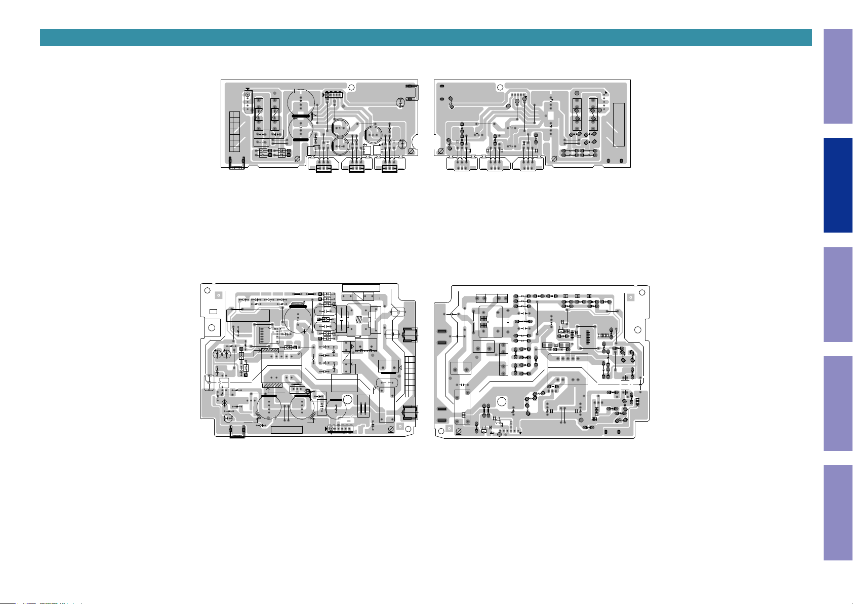
REGULATOR, SMPS
CUP13308Z
SMPS
MP
Sec.
Pri.
C6023
C6008 C6013
ZD620
R6017
R6021
C6010
REGULATOR (A Side)
CUP13032Z-1
REGULATOR PART
1.AC_S2
2.NC
3.RTN_GND
4.NC
5.AC_S2
AI SMT MI ICT FCT1 RP FCT2
BK303
1A387
MP_STAGE
CN302
1 5
T 1.25A L 250V
T 1.25A L 250V
F3003
F3004
T 1.25A L 250V
F3001
T 1.25A L 250V
F3002
C3003
C3005
C3004
C3007
J3004
J3006
D3001
D3003
D3002
D3004
3 .-12V
Pb
5.DA+5V
3.+12V
1.-12V
2.RLY_GND
4.VGND
C3006
2 .IN
BN301
5
J3025
J3024
J3023
BONDING
C3012
J3035
D3104
C3013
1 .GND
J3027
J3026
J3028
OIGI OGI G O
C3008
J3036
D3103
J3037
J3030
J3031
KIA7912 KIA7812
J3015
2 .GND
3 .+12V
IC301IC302
BK301
1A569-V1
C3024
D3101
D3108
J3013
Pb
C3001
1 .IN
1 .IN
2 .GND
3 .+5VV
J3033
J3034
J3032
IC305
KIA7805BPI
C3002
Pb
REGULATOR (B Side)
5.DA+5V
DA+5V TP
C3009
C3014
C3010
4.VGND
3.+12V
2.RLY_GND
1.-12V
-12V TP
+12V TP
15
C3011
AC_S2 TP
C3015
1.AC_S2
2.NC
3.RTN_GND
4.NC
5.AC_S2
AC_S2 TP
5 1
BAR CODE
This Unit
Before Servicing
Pb
BOTTOM SIDE BOTTOM SIDE BOTTOM SIDE
Electrical Mechanical Repair Information Updating
SMPS (A Side) SMPS (A Side)
IN
J6002 J6003
ZD608
R6008R6009
J6016
V
X
C
F
6
IC601
BONDING
VERSION
BONDING
J6005
D6005
C6003
D6004
C6004
D6002
ZD601
D
D6012
D6013
J6019
J6020
1 7
14 8
C6018
BONDING
ZD611
J6010
ZD613
ZD614
ZD617
ZD616
Pri.
Sec.
J6001
R6034
C6027
C6028
1.D5.2V
5.D_GND
4.D_GND
3.M_RESET
2.D5.2V
6.MAIN POWER
BN601
ZD609
ZD621
J6004
ZD610
J6017
BAR CODE
12 7
S
S
R6004
S
S
J6007
S
S
R6015
J6018
R6010
BONDING
D6007
J6009
ZD618
D6008
IC602
Pri.
T6001
Sec.
R6016
J6012
J6013
IC603
R6018
D6010
BONDING
C6019
ZD619
BK603
1A629
D6006
D6001
D6003
C6002
CX602
LF602
CLZ9Z126Z:E3,K
CLZ9Z133Z:E2,E1C
ZD612
ZD615
(AC220V~230V AREA)
(AC100V~120V AREA)
C6017
T1.6A L 250V
T2A L 250V
F6002
T 2.5A L 250V
T 5A L 250V
OPEN
6
(AC220V~240V AREA)
(AC100V~120V AREA)
3
OPEN
F6001
CX601
142
LF602
J6014
J6015
D6009
BONDING
CY602
BK601
J6011
1A834
CY601
CN602
CN601
LN
L N
C6001
AI FCT2RPFCT1ICTMISMT
2
Pri.
Sec.
BK602
1A834
1
4 3
RY601
Pb
L N
Pri.
Sec.
C6022
C6021
1 2
R6027
R6030R6029
R6028
4
3
C6011
R6011
17
N L
2 1
C6029
R6024
43
Pb
Q6003
MAIN_POWER TP
C6030
IC604
R6025
Pri.
Sec.
148
C6015
L6001
16
R6033R6032R6031
R6006
R6013
R6014
V
1
Q6002
X
C
F
C6026
6
D
C6014
C6009
C6007
C6006
C6005
127
S
S
R6012
S
S
C6012
S
S
R6022
R6023
C6020
R6019
R6020
D5.2V TP
Sec.
Pri.
Pri.
Sec.
C6024
C6025
R6026
22
Page 23
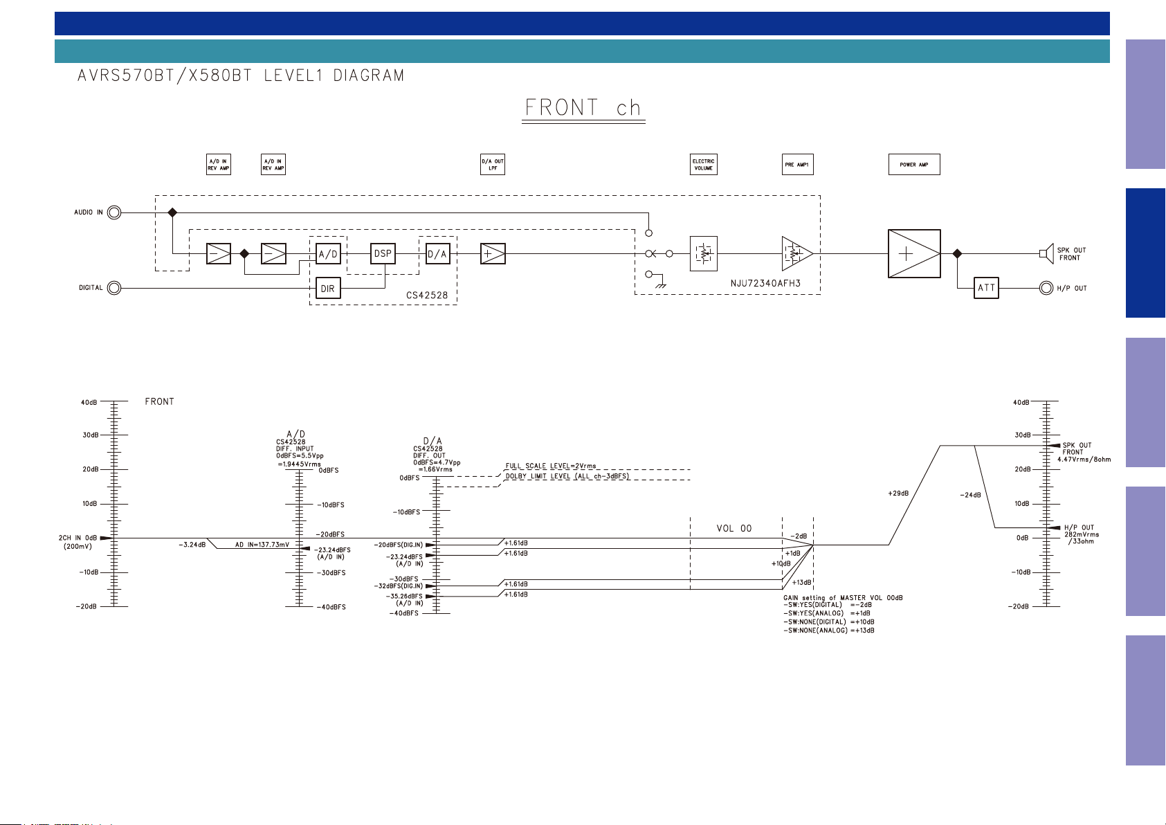
LEVEL DIAGRAM
FRONT ch
This Unit
Before Servicing
Electrical Mechanical Repair Information Updating
23
Page 24
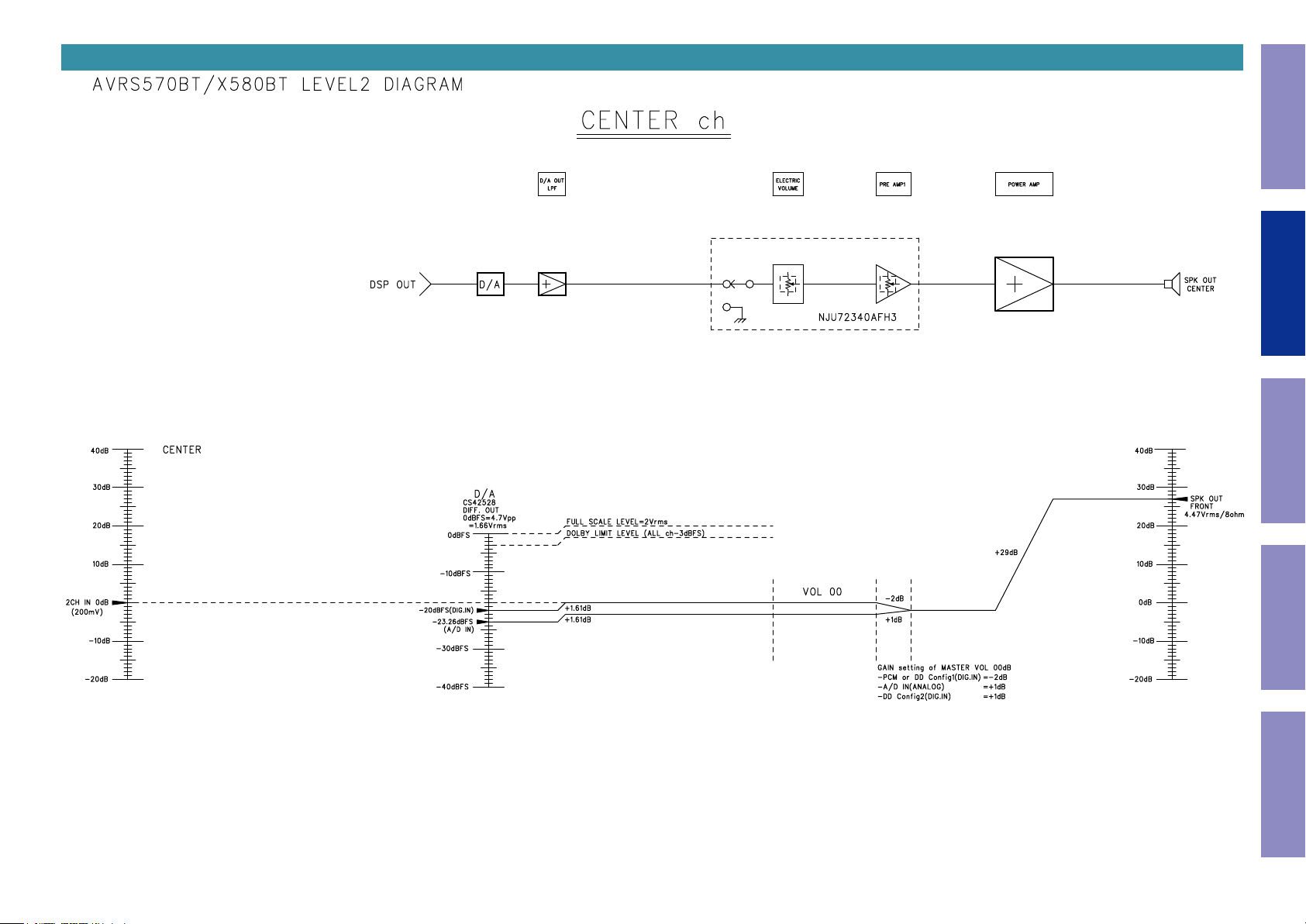
CENTER ch
This Unit
Before Servicing
Electrical Mechanical Repair Information Updating
24
Page 25

SURROUND ch
This Unit
Before Servicing
Electrical Mechanical Repair Information Updating
25
Page 26

SUBWOOFER ch
This Unit
Before Servicing
Electrical Mechanical Repair Information Updating
26
Page 27

BLOCK DIAGRAM
ANALOG AUDIO DIAGRAM
AVR-S570BT/X580BT ANALOG AUD IO BLOCK
This Unit
TU NER
AU DIO I N
SET UP M IC
FRO M DI GIT AL
AU DIO B LOC K
TU NER
FM
CB L/SAT
AU X
MIC
AD _FL
AD _FR
DA _FL
DA _FR
DA _CEN
DA _SW
DA _SL
DA _SR
USB /BT _IN
V+ :+7 .5V
* L OGIC CONT ROL HIGH LEV EL INP UT V OLT AGE( MIN: + 2.5V / MAX : V+)
V-: -7.5V
SEL ECT IC
NJU72750AV
InA /B1
InA /B2
InA /B3
InA /B4
InA /B5
InA /B6
InA /B7
DA0 1
DA0 2
DA0 3
DA0 4
DA0 5
DA0 6
OU TA1
MAIN
OU TA2
OU TA3
OU TB1
OU TB2
7in3o ut M atrix-Switch
OU TB3
ANA _AD _FL
ANA _AD _FR
H/ P OU T
H/ P L
GND
SP K O UT
+
-
+
-
+
-
+
-
+
-
H/ P R
FL
FR
CEN
SL
SR
VOLUME IC
NJU72343V
DA0 1
DA0 2
DA0 3
DA0 4
DA0 5
DA0 6
DA_ FL
ANA _FL
DA_ FR
ANA _FR
DA_ CEN
DA_ SW
DA_ SL
DA_ SR
V+ :+7 .5V
V-: -7.5V
* L OGIC CONT ROL HIGH LEV EL INP UT V OLT AGE( MIN: + 2.5V / MAX : V+)
MAIN AMP
Before Servicing
Electrical Mechanical Repair Information Updating
PR E OU T
MUT E
SW 1
SW 2
27
Page 28

DIGITAL AUDIO / HDMI DIAGRAM
AVR-S570BT/X580BT D IGITAL AUD IO/H D MI BLOCK
DI GTA L IN
US B IN
OP TICAL IN1
OP TICAL IN2
CO AXIA L IN1
HD MI IN 1
HD MI IN 2
HD MI IN 3
HD MI IN 4
DI R IN OPT ION
S570B T
X580B T
VDD:U SB3V 3
BT
MO DULE
USB
D+ /-
TMD S
TMD S
TMD S
TMD S
OP T IN
2
2
IPO D AU TH.
MFI 343S00177
UA RT
DE CORD ER
MLC 3730S
VDD33:U SB3V 3
VDD12:U SB1V 2
VDD:U SB3V 3
USB
I2C
CO AX IN
1
0
D IR/ COD EC
VD: +3V 3D
VD: +5V D
CS 42528
DIG ITAL
FILT ER
DA C
DA C
DA C
DA C
ANA LOG
DA C
FILT ER
DA C
LRC K
SCL K
SD0
SD1
SD2
CO DEC
SD3
SER IAL
PO RT
VO LUME
CO NTRO L
DA C
DA_ FL
DA_ FR
DA_ CEN
DA_ SW
DA_ SL
DA_ SR
This Unit
Before Servicing
DA C
+
AD C
-
+
AD C
-
DIG ITAL
FILT ER
DIG ITAL
FILT ER
GA IN
GA IN
&
CLI P
AD C
SER IAL
DA TA
&
CLI P
SER IAL
AU DIO I/ F
+3V 3D
Electrical Mechanical Repair Information Updating
DE M
INP UT
SEL ECT
AU DIO D AC
I2S
(PC M5102A)
CPV DD: 3V3
DVDD: 3V3
SN74A HC157P WR
HD MI_S DAT A0
HD MI_S DAT A1
HD MI_S DAT A2
HD MI_S DAT A3
HD MI_L RCLK
HD MI_S CLK
HD MI_M CLK
HD MI MC LK
MCLK
IN3
P3 R X
IN2
P2 R X
IN1
P1 R X
IN0
P0 R X
S.F LASH
32M
For GUI
VCC:C EC3V 3
VDD09ST B: CE C0V 9
VDD09:C EC0V 9COR E
AVDD18: CEC1 V8
AVDD33: CEC3 V3
H DMI TX (8K )
MN 864807A
ARC /eAR C
SPDI F (FO R ARC )
HD MI_S PDIF
OUT 0
P0T X
P1T X
OUT 1
MU X
VCC:+ 3V3D
CLK /DA TA
Rx
REC OVER Y
+3V 3D
S/P DIF
DE COD ER
SAI_ LRCK
SAI_ SCLK
VDDA: +3V3 D
VDDIO: +3V 3D
D SP
SAI_ SDO
--
AD _FL
--
AD _FR
DA_ FL
DA_ FR
DA_ CEN
DA_ SW
DA_ SL
DA_ SR
USB /BT _IN
TO ANA LOG
AU DIO B LOC K
OMC K
RMC K
DAO _MC K
XOU T
LRC K
SCL K
SD0
SD1
SD2
SD3
VDD:+ 1V8H
CS 497024
HD MI O UT
ARC /eAR C
S.F LASH
8M
VCC:+ 3V3D
SD RAM
16M
VCC:+ 3V3D
28
Page 29

VIDEO DIAGRAM
AVR-S570BT/X580BT VID EO BLOCK
This Unit
Before Servicing
Electrical Mechanical Repair Information Updating
HD MI IN
HD MI IN 1
(CB L/SAT )
HD MI IN 2
(Me dia Play er)
HD MI IN 3
(B lu-ra y)
HD MI IN 4
(GAME )
P3 RX
P2 RX
P1 RX
P0 RX
P3 RX
P2 RX
P1 RX
P0 RX
HDMI TX(MN864807A)
MAIN
SUB
S.F LASH
32M
VCC:C EC3V 3
P1 T X
ARC /eAR C
P0 T X
CEC 5V
CEC 3V3
CEC 1V8
CEC 0V9
CEC 0V9C ORE
25.000MH z
HD MI O UT
MO NITO R OUT
29
Page 30

POWER DIAGRAM
AVR-S570BT /X 580BT VCC D IAGRAM
!
AC C OR D
REL AY
!
S1 (AMP+ B,-B )
S2 (+12V ,-12V)
MAIN T RAN S
!
!
INP UT C URRENT (Re f Vola ge: 5.2V )
SM PS Tot al C urren t : A bou t 4291.242m A
D
S
43
G
S4 (FL+ Vdi sp)
S5 (FILAME NT)
*D C-DC Effie cienc y:85%
2 1
+5 .2V
MAIN P WR O N
HI +B
LO W+B
HI -B
LO W-B
MAIN+ B
2
4
1
3
TFZ V7.5 B
BU33T D3W G
KIA 7805BPI
KIA 7812BPI
KIA 7912PI
30mA
TLV 75712PDB VR
USB _PO WER1
20mA
85mA
1500mA
300mA
385.5m A
500.1m A
626.2m A
233mA
158mA
500mA
120.08m A
1205mA
2100mA
CEC _PO WER2
DA _POW ER
(5. 2V)
TP S563201DDCR( +3.3 V)
1218.58m A
D5 V
TP S563201DDCR( +1.8 V)
246.84m A
CEC _PO WER3
TP S563201DDCR( 0.9V )
239.84m A
CEC _PO WER
TP S563201DDCR( 0.9V )
417.98m A
CEC _PO WER
BD 2222G-GTR
H5 VOUT _PO WER
DA _POW ER
CEC _PO WER
USB _PO WER2
CPU _PO WER
SH ORT
DA _POW ER
(H DMI C EC C ONTR OL/SN74C BT3251P WR)
SW M5V
MCU +5V
FRO NT L ED(C VDB LBJE GJ204L)
CS42528( VD)
+5 VD
USB / B U12TD 3WG
D5 V
HD MI OU T JA CK
CEC 5V
+3 V3D /DIR ,DSP ,OPT JACK
(CS 497024,CS42528,M 12L16161A5 TG2R ,MX25L 8006EM2I- 12G,SN74A HC157P WR, J SR1124*2)
CEC 3V3 /HD MI
(MN 864807A, SN 74AXC 8T245x2 , MX25L 3233FM2I -08G)
USB 3V3 /MLC 3730S,W9864G 6JH- 6, MX 25L1606EM2 I-12G, B T MO DUL E, IPO D CP
USB 1V2
(ML C3730S)
MC U+3V 3/M ICOM
(ST M32F101ZG ,M24C32W MN6 TP,V FD)
SW M3V3 (PRO TEC T, CE C)
+1 V8/D SP
(CS 497024)
CEC 1V8
(MN 864807A, SN 74AXC 8T245x2 )
CEC 0V9
(MN 864807A)
CEC 0V9 CORE
(MN 864807A)
TFZ V7.5 B
MAIN-B
178mA
REL AY* 5
+7 .5V
SEL ETOR IC,V OLUM E IC
54mA
(NJ U72750AV, NJU72343V, NJM8080G )
A+ 12V
30mA
(NJ M8080 X 3 , NJM 4580 X 1)
45mA
DA +3.3 V
85mA
+5 VA
50mA
TU NER+ 5V
A-12V
(NJ M8080 X 3 , NJM 4580 X 1)
-7.5 V
SEL ETOR IC,V OLUM E IC
(NJ U72750AV, NJU72343V, NJM8080G )
49mA
Vdi sp(+ 37V)
163mA
FILAME NT A C
FILAME NT A C
This Unit
Before Servicing
(US B DA C:PC M5102A)
(CS 42528-CQ, NJM2740V X 2, TUNE R)
S2 TO TAL : 442.430mA
Electrical Mechanical Repair Information Updating
30
Page 31

WIRING DIAGRAM
AVR-S570BT/X580BT WIRING D IAGRAM
CN602
2P
SM PS< -AC I N
AC C ORD
SM PS< -DIG ITA L
This Unit
D IGITAL PCB
CN771
5P
CN751
6P
CN711
27P
CN772
13P
CN752
5P
CN713
CN712
11P
11P
Before Servicing
TRANS
TR ANS - > FR ONT
6P
SM PS PCB
BN101_1
9P
POW ER L ED< ->FR ONT
9P
BN101
FUN CTIO N
ENC ODE R
PO WER
LED PCB
CN102
CN601
TR ANS < - SM PS
TRA NS -> REG UL.
TR ANS-> MAIN
3P
CN104
2P
5P
REG ULA TOR PCB
CN302
H/ P <- MAIN
3P
BN131
BN601
7P
H /P PCB
CN103
3P
H/ P-FRO NT
MIC PCB
BN301
5P
REG UL.< - DIG ITAL
Electrical Mechanical Repair Information Updating
BN502
MAIN-> DIG ITAL
11P
BN505
3P
FRO NT PCB
BN12A
5P
5P
BN12B
MIC
BT MOD ULE
BN501
MAIN-> DIG ITAL
13P
7P
CN503
(FFC )
MAIN PCB
FRO NT < -> D IGIT AL
27P
BN12B 1
US B & BT <-> DIG ITAL
10P
(FFC )
CN911
USB
10P
US B & BT PCB
BN914
5P
11P
BN912
US B & BT <-> DIG ITAL
31
Page 32

PC13-TAMPER-RTC
SEMICONDUCTORS
Only major semiconductors are shown, general semiconductors etc. are omitted to list.
The semiconductor which described a detailed drawing in a schematic diagram are omitted to list.
1. IC's
STM32F101ZE (DIGITAL : IC711)
DD_3VSS_3
V
144
143
PE2
1
PE3
2
PE4
3
PE5
4
PE6
5
VBAT
6
V
SS_5
V
DD_5
PF10
OSC_IN
OSC_OUT
NRST
V
SSA
V
REF-
V
REF+
V
DDA
PA0-WKUP
7
8
9
PF0
10
PF1
11
PF2
12
PF3
13
PF4
14
PF5
15
16
17
PF6
18
PF7
19
PF8
20
PF9
21
22
23
24
25
26
PC0
27
PC1
28
PC2
29
PC3
30
31
32
33
34
35
PA1
36
PA2
3738394041424344454647484950515253545556575859
PA3
SS_4
V
PC14-OSC32_IN
PC15-OSC32_OUT
STM32F101ZG Terminal Functions
Pin Pin Name Symbol
1 PE2 DC_PROTECT
2 PE3 USB_DAC_MUTE
3 PE4 POWER_DOWN
4 PE5 FRONT_RLY(SPK_RLY_ON)
5 PE6 C/S_RLY
6 VBAT VBAT
7 PC13 MIC_DET
8 PC14 / OSC32_IN OSC32_IN
PC15 / OSC32_
9
OUT
10 PF0 ISEL_B
11 PF1 ISEL_A
12 PF2 HI-B_RLY
13 PF3 SEL_CLK
14 PF4 SEL_DATA
15 PF5 CP_SDA_NC
16 VSS_5
17 VDD_5
18 PF6 DIR INT(NC)
19 PF7 USB_EN
20 PF8 MAIN_VOL_MUTE
OSC32_OUT
PE1
PE0
PB9
PB8
BOOT0
142
141
140
139
138
PA4
PA5
PA6
PA7
DD_4
V
I/O Pullup STBY
O - O/L O/L O/L O/L
O - O/L O/L O/L O/L
O - O/L O/L O/L O/L
O - O/L O/L O/L O/L
O - O/L O/L O/L O/L
O - O/L O/L O/L O/L
O - O/L O/L O/L O/L
O/L - O/L O/L O/L O/L
O - O/L O/L O/L O/L
O - O/L O/L O/L O/L
DD_11VSS_11
PB7
PB6
PB5
PB4
PB3
PG15
V
PG14
PG13
137
136
135
134
133
132
131
130
129
128
LQFP144
PB0
PB1
PB2
PC4
PC5
PF11
PF12
PF13
DD_6
VSS_6
V
PG12
127
PF14
PassTrough
PG11
PG10
PG9
PD7
126
125
124
123
PG0
PG1
PF15
DD_10VSS_10
PD6
V
PD5
122
121
120
119
60
6162636465666768697071
PE7
PE8
PE9
SS_7
DD_7
V
V
BT
STBY
I M3VPu I I I I
I M3VPu I I I I
- - - - - -
I Pd I I I I
- - - - - -
- - - - - -
I Pu I I I I
I Pu I I I I
- - - - - -
- - - - - -
PD4
PD3
PD2
PD1
PD0
PC12
PC11
PC10
PA15
PA14
118
117
116
PE10
PE11
PE12
stop
109
115
114
113
112
111
110
108
V
DD_2
107
V
SS_2
106
NC
105
PA13
104
PA12
103
PA11
102
PA10
101
PA9
100
PA8
99
PC9
98
PC8
97
PC7
96
PC6
95
V
DD_9
94
V
SS_9
93
PG8
92
PG7
91
PG6
90
PG5
89
PG4
88
PG3
87
PG2
86
PD15
85
PD14
84
V
DD_8
83
V
SS_8
82
PD13
81
PD12
80
PD11
79
PD10
78
PD9
77
PD8
76
PB15
75
PB14
74
PB13
73
PB12
72
PE13
PE14
PE15
PB10
PB11
SS_1
DD_1
V
V
Function
DC Protection Detect
USB_DAC_MUTE control
Power Down Detect
Front SPK RLY control
Surround SPK RLY control/Center SPK RLY
control
3.3V
MIC_DET Detect
FUNCTION ENDORDER input(A)
FUNCTION ENDORDER input(B)
HI-B_RLY control
NJU72750AV SEL CLK
NJU72750AV SEL DATA
APPLE AUTH CHIP_I2C_SDA (for AVR-
X250BT)
GND Fixed
3.3V
DIR _INTERRUPTT(NC)
USB_CURRENT IC control
Volume Mute line
Pin Pin Name Symbol
21 PF9 MAIN_VOL_DATA
22 PF10 MAIN_VOL_CLK
23 PH0 / OSC_IN XTAL_IN
24 PH1 / OSC_OUT XTAL_OUT
25 NRST RESET
26 PC0 KEY1
27 PC1 KEY2
28 PC2 KEY3
29 PC3 OPTION
30 VSSA
31 VREF32 VREF+
33 VDDA
34 PA0 / WKUP CP_SCL_NC
35 PA1 USB_RESET
36 PA2 USB_RX
37 PA3 USB_TX
38 VSS_4
39 VDD_4
40 PA4 DSP_CS
41 PA5 DSP_CLK
42 PA6 DSP_MISO
43 PA7 DSP_MOSI
44 PC4 HDMI_TEST_NC
45 PC5 TX_TEMP
46 PB0 DIR_MISO
47 PB1 DIR_CLK
48 PB2 / BOOT1 BOOT1
49 PF11 DIR_MOSI
50 PF12 DSP_RST
51 VSS_6
52 VDD_6
53 PF13 DSP_MODE_SEL
54 PF14 CODEC_MUTE
55 PF15 DIR_RST
56 PG0 DIR_CE
57 PG1 DSP_SPC1_IRQ
58 PE7 DSP_PCP_BSY
59 PE8 CEC_POWER
60 PE9 HDMI_SW
61 VSS_7
62 VDD_7
63 PE10 DV5_POWER
64 PE11 H5VOUT_POWER
65 PE12 HPD1
66 PE13 HPD2
67 PE14 HPD3
68 PE15 HPD4
69 PB10 HPD5_NC
BT
I/O Pullup STBY
PassTrough
STBY
stop
O - O/L O/L O/L O/L
O - O/L O/L O/L O/L
I - - - - -
O - - - - -
I - - - - -
I M3VPu I I I I
I M3VPu I I I I
I M3VPu I I I I
I M3VPu I I I I
- - - - - -
- - - - - -
- - - - - -
- - - - - -
O - O/L O/L O/L O/L
O - O/L O/L O/L O/L
USB3V3Pu
O
I
O/L O/L O/L O/L
USB3V3Pu
I I I I
- - - - - -
- - - - - -
O - O/L O/L O/L O/L
O D3VPu O/L O/L O/L O/L
I D3VPu I I I I
O - O/L O/L O/L O/L
O - O/L O/L O/L O/L
I - I I I I
I - I I I I
O - O/L O/L O/L O/L
I - - - - -
O - O/L O/L O/L O/L
O - O/L O/L O/L O/L
- - - - - -
- - - - - -
Pull Down
I/O
O/L O/L O/L O/L
I(FT) - O/L O/L O/L O/L
O - O/L O/L O/L O/L
O - O/L O/L O/L O/L
I D3VPu I I I I
I D3VPu I I I I
O - L H L O/L
O - O/L O/L O/L O/L
- - - - - -
- - - - - -
O - O/L H H O/L
I - I I I I
O - O/L O/L O/L O/L
O - O/L O/L O/L O/L
O - O/L O/L O/L O/L
O - O/L O/L O/L O/L
O - O/L O/L O/L O/L
Function
Volume Data line
Volume CLK line
8Mhz Xtal
8Mhz Xtal
RESET
KEY1 input
KEY2 input
KEY3 input
MODEL OPTION
GND Fixed
GND Fixed
3.3V
3.3V
APPLE AUTH CHIP_I2C_SCL (for AVR-
X250BT)
BX8804(USB DECORDER) RESET control
BX8804(USB DECORDER) RX control
BX8804(USB DECORDER) TX control
GND Fixed
3.3V
DSP Chip Select
DSP_CLK
DSP MISO
DSP MOSI
HDMI_TEST_Port (Temp)
Temperature detection for HDMI Tx
(MN864807) (A/D converter)
DIR_MISO
DIR_CLK(separated from AVR1312 DSP_
CLK)
GND Fixed
DIR MOSI(separated from AVR1312 DSP_
MOSI)
DSP Reset control
GND Fixed
3.3V
DSP_MODE_SEL
CODEC Mute Detect(*FT = 5V tolerant)
DIR Reset
DIR Chip Select
DSP INTERRRUPTQ
DSP BSY
CEC_POWER TIMING control
HDMI Audio Data MCLK Select SW
GND Fixed
3.3V
DV5_POWER TIMING control
HDMI-Tx_5V_Power_Control
HDMI INPUT1 HOT PLUG CONTROL
HDMI INPUT2 HOT PLUG CONTROL
HDMI INPUT3 HOT PLUG CONTROL
HDMI INPUT4 HOT PLUG CONTROL
HDMI INPUT5 HOT PLUG CONTROL
This Unit
Before Servicing
Electrical Mechanical Repair Information Updating
32
Page 33

Pin Pin Name Symbol
70 PB11 HPD6_NC
71 VSS_1
72 VDD_1
73 PB12 HDMI_OSD_CS
74 PB13 HDMI_OSD_SCLK
75 PB14 HDMI_OSD_MISO
76 PB15 HDMI_OSD_MOSI
77 PD8 DA_POWER
78 PD9 USB_POWER1
79 PD10 CEC_OUT
80
PD11
AUDIO_OE
81 PD12 FLASH_OE
82
PD13 AUDIO_OE_TEST
83 VSS_8
84 VDD_8
85 PD14 HDMI_SCL
86 PD15 H5V_DET
87 PG2 HINSEL_A
88 PG3 HINSEL_B
89 PG4 HINSEL_C
90 PG5 MAIN_POWER
91 PG6 CPU_POWER
92 PG7 VOL+
93 PG8 VOL94 VSS_9
95 VDD_9
96 PC6 PWR_FAIL_PROTECT
97 PC7 VFD_CE
98 PC8 VFD_CLK
99 PC9 THERMALDET_B
100 PA8 VFD_DATA
101 PA9 UPDATE_TX
102 PA10 UPDATE_RX
103 PA11 THERMALDET_A
104 PA12 MN864788_HAINT0(NC)
105 PA13 DEBUG
106 PCAP_2
107 VSS_2
108 VDD_2
109 PA14 DEBUG
110 PA15 DEBUG
111 PC10 TX_HINT
112 PC11 TX_HAINT
113 PC12 ASO_DET
114 PD0 VFD_RST
115 PD1 HP_RLY
116 PD2 USB_POWER2
117 PD3 WAKE_UP
118 PD4 HP_DET
119 PD5 GRN_LED
120 VSS_10
121 VDD_10
122 PD6 MN864807_HSCL
123
PD7 REMOTE_IN
124 PG9 MN864807_HSDA
125 PG10 EEPROM_SDA
126 PG11 EEPROM_SCL
127 PG12 DAC_MUTE(NC)
BT
I/O Pullup STBY
O - O/L O/L O/L O/L
- - - - - -
- - - - - -
O +3VHPu O/L O/L O/L O/L
O - O/L O/L O/L O/L
I - I I I I
O - O/L O/L O/L O/L
O - L L L O/L
O - O/L O/L H O/L
O - O/L O/L O/L O/L
I +3VHPu I I I I
I +3VHPu I I I I
I/O +3VHPu O/L O/L O/L O/L
- - - - - -
- - - - - -
O - O/L O/L O/L O/L
I - I I I I
O - O/L O/L O/L O/L
O - O/L O/L O/L O/L
O - O/L O/L O/L O/L
O - O/L O/L O/L O/L
O - O/L O/L O/L O/L
I Pu I I I I
I Pu I I I I
- - - - - -
- - - - - -
I M3VPu I I I I
O - O/L O/L O/L O/L
O - O/L O/L O/L O/L
I M3VPu I I I I
O - O/L O/L O/L O/L
O M3VPu - - - -
I M3VPu - - - -
I M3VPu I I I I
CEC3VPu
I
I - - - - -
- - - - - -
- - - - - -
- - - - - -
I - - - - -
I - - - - -
CEC3VPu
I
I Pd I I I I
I M3VPu I I I I
O - O/L O/L O/L O/L
O - O/L O/L O/L O/L
O - O/L O/L H O/L
I M3VPu I I I I
I Pu I I I I
O - O/L O/L O/L O/L
- - - - - -
- - - - - -
CEC3VPu
I/O
I M3VPu I I I I
CEC3VPu
I/O
I/O M3VPu O/L O/L O/L O/L
O M3VPu O/L O/L O/L O/L
O - O/L O/L O/L O/L
PassTrough
I I I I
I I I I
O/L O/L O/L O/L
O/L O/L O/L O/L
STBY
stop
Function
HDMI INPUT6 HOT PLUG CONTROL
GND Fixed
3.3V
MN864807 OSD Chip Select
MN864807 OSD Clock
MN864807 O8D DATA input
MN864807 OSD DATA output
DA_POWER TIMING control
USB_POWER1(1.2V) TIMING control
CEC MODE control
Audio Buffer IC(I2S3.3 Out) OE Control
Flash Buffer IC OE Control
Audio Buffer IC(I2S1.8 In) OE Control
GND Fixed
3.3V
HDMI SCL
HDMI CEC STBY_H5_DET
HDMI CEC STBY_HINSEL_A
HDMI CEC STBY_HINSEL_B
HDMI CEC STBY_HINSEL_C
POWER RELAY control
MCU POWER PULL UP SWITCHING
VOLUME UP
VOLUME DOWN
GND Fixed
3.3V
+12V/-12V CHECK PROTECTION
VFD_CE
VFD_CLK
TEMPERATURE PROTECTION
VFD_DATA
UPDATE TX
UPDATE RX
TEMPERATURE PROTECTION
MN864788_HDMI AUDIO INTERRUPT0(NC)
JTMS / SWDIO
Not Connected
GND Fixed
3.3V
JTCK / SWCLK
JTDI
MN864807_HDMI INTERRUPT
MN864807_HDMI AUDIO INTERRUPT1
ASO_DETECT
VFD_RESET(Low Active)
H/P RLY control
USB_POWER2(3.3V) TIMING control
WAKE UP
H/P DETECT
2COLOR LED GREEN
GND Fixed
3.3V
MN864807_I2C_SCL
REMOTE input(invert as AVR1312))
MN864807_I2C_SDA
EEPROM SDA
EEPROM SCL
NC(DAC Mute control)
Pin Pin Name Symbol
128 PG13 TUNER_SCLK
129 PG14 TUNER_SDIO
130 VSS_11
131 VDD_11
132 PG15 TX_RST
133 PB3 DEBUG
134 PB4 DEBUG
135 PB5 SUB MUTE
136 PB6 CEC_CTL1
137 PB7 CP_RESET_NC
138 BOOT0 BOOT0
139 PB8 TUNER_CE
140 PB9 TUNER_INT
141 PE0 TUNER_RST
142 PE1 RED_LED
143 VSS_3
144 VDD_3
BT
I/O Pullup STBY
O - O/L O/L O/L O/L
I/O - O/L O/L O/L O/L
- - - - - -
- - - - - -
O Pd O/L O/L O/L O/L
O - - - - -
I - - - - -
O - O/L O/L O/L O/L
I - I I I I
O - O/L O/L O/L O/L
I Pd I I I I
O - O/L O/L O/L O/L
I - I I I I
O - O/L O/L O/L O/L
O - O/L H H O/L
- - - - - -
- - - - - -
PassTrough
STBY
stop
Function
TUNER SCLK
TUNER SDIO
GND Fixed
3.3V
MN864807_RESET
JTDO / TRACESWO
NJTRST
Sub Woofer MUTE
CEC IN_CEC_CTL1
APPLE AUTH_CHIP_RESET (for AVR-X250BT)
UPDATE BOOT(HIGH:UPDATE /
LOW:NORMAL MODE)
TUNER CE
TUNER INTERRUPT
TUNER Reset control
2COLOR LED RED
GND Fixed
3.3V
This Unit
Before Servicing
Electrical Mechanical Repair Information Updating
33
Page 34

M24C32WMN6TP (DIGITAL : IC712)
M24128, M24C64, M24C32 Description
Table 2. Signal names
Signal name Function Direction
E0, E1, E2 Chip Enable Input
SDA Serial Data I/O
SCL Serial Clock Input
WC Write Control Input
V
CC
V
SS
Figure 2. DIP, SO, TSSOP and UFDFPN connections
Supply voltage
Ground
M24128
M24C64
M24C32
1
E0 V
2
3
E2
4
SS
MX25L3233FM2I-08G (DIGITAL : IC725)
8
CC
7
WCE1
6
SCL
5
SDAV
AI01845e
Block diagram
4. PIN DESCRIPTION
SYMBOL DESCRIPTION
This Unit
Before Servicing
Note:
Electrical Mechanical Repair Information Updating
34
Page 35

CS497024CVZ (DIGITAL : IC741)
MX25L8006EM2I-12G (DIGITAL : IC742)
PIN DESCRIPTION
CS#
SO/SIO1
WP#
GND
1
2
3
4
8
7
6
5
VCC
HOLD#
SCLK
SI/SIO0
SYMBOL
CS#
SI/SIO0
SO/SIO1
SCLK
WP#
HOLD#
VCC
GND
DESCRIPTION
Chip Select
Serial Data Input (for 1 x I/O)/ Serial Data
Input & Output (for Dual Output mode)
Serial Data Output (for 1 x I/O)/ Serial Data
Output (for Dual Output mode)
Clock Input
Write protection
Hold, to pause the device without
deselecting the device
+ 3.3V Power Supply
Ground
This Unit
Before Servicing
Electrical Mechanical Repair Information Updating
Block diagram
35
Page 36

M12L16161A5TG2R (DIGITAL : IC743)
V
DD
DQ0
DQ1
V
SSQ
DQ2
DQ3
V
DDQ
DQ4
DQ5
V
SSQ
DQ6
DQ7
V
DDQ
LDQM
WE
CAS
RAS
CS
BA
A10/AP
A0
A1
A2
A3
V
DD
1
2
3
4
5
6
7
8
9
10
11
12
13
14
15
16
17
18
19
20
21
22
23
24
25
50
49
48
47
46
45
44
43
42
41
40
39
38
37
36
35
34
33
32
31
30
29
28
27
26
V
SS
DQ15
DQ14
V
SSQ
DQ13
DQ12
V
DDQ
DQ11
DQ10
V
SSQ
DQ9
DQ8
V
DDQ
N.C/RFU
UDQM
CLK
CKE
N.C
A9
A8
A7
A6
A5
A4
V
SS
I/O Control
LWE
LDQM
Output Buffer
DQi
LDQM
ADD
CLK
LCKE
Address Register
LRAS LCBR
CLK
Bank Select
Refresh Counter
LRAS
CKE
Row Buffer
LCBR
LWE
CS
Data Input Register
Row Decoder
Col. Buffer
Column Decoder
Latency & Burst Length
Programming Register
LCAS
Timing Register
RAS CAS WE
512K x 16
512K x 16
Sense AMP
LWCBR
L(U)DQ M
Terminal Functions
Pin Name Input Function
CLK System Clock Active on the positive going edge to sample all inputs.
CE Chip Select
CKE Clock Enable
A0 ~ A10/AP Address
BA Bank Select Address
RAS Row Address Strobe
CAS Column Address Strobe
WE Write Enable
L(U)DQM Data Input / Output Mask
DQ0 ~ 15 Data Input / Output Data inputs/outputs are multiplexed on the same pins.
VDD/VSS Power Supply/Ground Power and ground for the input buffers and the core logic.
VDDQ/VSSQ Data Output Power/Ground
N.C/RFU No Connection/ Reserved for Future Use This pin is recommended to be left No Connection on the device.
Disables or enables device operation by masking or enabling all inputs except
CLK, CKE and L(U)DQM.
Masks system clock to freeze operation from the next clock cycle. CKE should
be enabled at least one cycle prior to new command.
Disable input buffers for power down in standby.
Row / column addresses are multiplexed on the same pins.
Row address : RA0 ~ RA10, column address : CA0 ~ CA7
Selects bank to be activated during row address latch time. Selects bank for
read/write during column address latch time.
Latches row addresses on the positive going edge of the CLK with RAS low.
Enables row access & precharge.
Latches column addresses on the positive going edge of the CLK with
CAS low.
Enables column access.
Enables write operation and row precharge.
Latches data in starting from CAS, WE active.
Makes data output Hi-Z, tSHZ after the clock and masks the output. Blocks data
input when L(U)DQM active.
Isolated power supply and ground for the output buffers to provide improved
noise immunity.
CS42528-CQ (DIGITAL : IC744)
This Unit
Before Servicing
Electrical Mechanical Repair Information Updating
Block diagram
36
Page 37

Terminal Functions
GND
C
GND 1 VBST
DDC Package
SN74AHC157PWR (DIGITAL : IC745)
V
1
16
/B
A
C
G
2
15
1A
4A
3
14
1B
4B
4
13
1Y
4Y
5
12
2A
3A
6
11
2B
3B
7
10
2Y
3Y
8
9
INPUTS OUTP
G A/B A B Y
HXXXL
LLLXL
LLHX H
LHXL L
LHXHH
2
1A
3
1B
5
2A
6
2B
11
3A
UT
10
3B
14
4A
13
4B
15
G
1
A/B
4
1Y
7
2Y
This Unit
9
3Y
12
4Y
Before Servicing
TPS563201 (DIGITAL : IC751 - IC754)
6-Pin SOT
Top View
SW 2 EN5
VIN 3 VFB4
Terminal Functions
PIN
NAME NUMBER
I/O DESCRIPTION
Ground pin Source terminal of low-side power NFET as well as the ground
GND 1 —
terminal for controller circuit. Connect sensitive VFB to this GND at a single
point.
SW 2 O Switch node connection between high-side NFET and low-side NFET.
VIN 3 I Input voltage supply pin. The drain terminal of high-side power NFET.
VFB 4 I
Converter feedback input. Connect to output voltage with feedback resistor
divider.
EN 5 I Enable input control. Active high and must be pulled up to enable the device.
VBST 6 O
Supply input for the high-side NFET gate drive circuit. Connect 0.1 µF
capacitor between VBST and SW pins.
EN 5
6
VFB 4
Voltage
Reference
Soft Start
Threshold
V
UVP
+
Hiccup
Control Logic
UVP
+
OVP
V
OVP
PWM
Ref
+
+
SS
t
ON
One-Shot
TSD
OCL
OCL
+
+
ZC
Regulator
UVLO
XCON
3 VIN
VREG5
6 VBST
HS
2 SW
VREG5
LS
1 GND
Electrical Mechanical Repair Information Updating
37
Page 38

NJU72750A (DIGITAL : IC770)
17
17
32
61 1
No. Symbol Function No. Symbol Function
1 V+ Power supply(+) 17 DATA IC control data input
2 InA1 Ach input1 18 CLOCK IC control clock input
3 InB1 Bch input1 19 NC 4 InA2 Ach input2 20 NC 5 InB2 Bch input2 21 OutB3 Bch output3
6 InA3 Ach input3 22 OutA3 Ach output3
7 InB3 Bch input3 23 REF_B Bch reference potential
8 InA4 Ach input4 24 OutB2 Bch output2
9 InB4 Bch input4 25 OutA2 Ach output2
10 InA5 Ach input5 26 REF_A Ach reference potential
11 InB5 Bch input5 27 OutB1 Bch output1
12 InA6 Ach input6 28 OutA1 Ach output1
13 InB6 Bch input6 29 NC 14 InA7 Ach input7 30 ADR0 Address selection pin 0
15 InB7 Bch input7 31 ADR1 Address selection pin 1
16 REF BIAS reference potential 32 V- Power supply(-)
NJU72343 (DIGITAL : IC771)
32
61 1
No. Symbol Function No. Symbol Function
1 AREF Analog reference potential 17 DATA IC control data input
2 ADR Address selection 18 CLOCK IC control clock input
3 InA2 Ach input2 19 VDDOUT Digital power supply output
4 InB2 Bch input2 20 AREF Analog reference potential
5 InA1 Ach input1 21 OutH Hch output
6 InB1 Bch input1 22 OutG Gch output
7 InC Cch input 23 OutF Fch output
8 InD Dch input 24 OutE Ech output
9 InE Ech input 25 OutD Dch output
10 InF Fch input 26 OutC Cch output
11 InG1 Gch input1 27 OutB Bch output
12 InH1 Hch input1 28 OutA Ach output
13 InG2 Cch input2 29 AREF Analog reference potential
14 InH2 Dch input2 30 V- Power supply(-)
15 MUTE External mute control 31 AREF Analog reference potential
16 REF Digital reference potential 32 V+ Power supply(+)
This Unit
Before Servicing
Electrical Mechanical Repair Information Updating
38
Page 39

MLC3730S (USB : IC2006)
Pin Descriptions
No.-
BGA Ball
1-D4 VDD33IO POWER VDD 3.3V Digital I/O Power
2-E5 VSS33IO GND VSS 3.3V Digital I/O Ground
3-B1 PGPA09 BS I2C1-SCL HU3_CTS
4-C1 PGPA10 BS TOUT1
5-C2 PGPA11 BS I2C1-SDA HU3-RDY
6-D2 PGPA12 BS AMCLK0-out AMCLK0-In PCM0-SYNC
7-D1 PGPA13 BS ALRCLK0-out ALRCLK0-In PCM0-CLK
8-E1 PGPA14 BS ABCLK0-out ABCLK0-In PCM0-DI
9-E2 PGPA15 BS ADO0-0 ADI0-0 PCM0-DO
10-E4 PGPB00 BS ADO0-1 ADI0-1
11-F2 PGPB01 BS AMCLK1-Out AMCLK1-In PCM1-SYNC ADO1-2
12-F1 PGPB02 BS ALRCK1-Out ALRCK1-In PCM1-CLK ADO0-3 ADI0-2
13-G1 PGPB03 BS ABCLK1-Out ABCLK1-In PCM1-DI ADO1-3 ADI1-2
14-G2 PGPB04 BS ADO1-0 ADI1-0 PCM1-DO
15-F4 PGPD04 BS HU4-RDY
16-H2 PGPB05 BS ADO1-1 ADI1-1 DRVVBUS20
17-G5 PGPD13 BS HU4-TXD
18-H1
19-G4 PGPD14 BS HU4-RXD
20-J1
21-H4 PGPD15 BS HU4-CTS PAD19 NAND-CEB2 S
22-J2 PGPB08 BS HU4-CTS SDIO3-CLK DRVVBUS20 PECSN
23-J4 VDD12INT POWER VDD 1.2V Digital Internal Core Power
24-J5 VSS12INT GND VSS 1.2V Digital Internal Core Ground
25-K2 PGPB09 BS HU4-RDY SDIO3-CMD PEOEN
26-K4 PGPC12 BS SDIO1-D1 NAND-REB PAD22
27-K1 PGPB10 BS HU2-TXD NMWBE1 SDIO3-D0 PAD22
28-L4 PGPC13 BS SDIO1-D2 NAND-WEB PECSN
29-L1 PGPB11 BS HU2-RXD NMWBE0 SDIO3-D1 PAD21
30-L5 PGPC14 BS SDIO1-D3 NAND-CEB0 PEOEN
31-L2 PGPB12 BS HU2-CTS ECSN1 SDIO3-D2 PAD20
32-M4 PGPC15 BS
33-M2 PGPB13 BS HU2-RDY ECSN2 SDIO3-D3 PAD19
34-M1 PGPB14 BS EMCLK-0 UCLK NAND-CLE
35-N1 PGPB15 BS ELRCK
36-N4 PGPC00 BS EBCLK SDIO1-D1 NAND-REB
37-N2 PGPC01 BS EDI SDIO1-D2 NAND-WEB
38-P2 PGPC02 BS ESCOR SDIO1-D3 NAND-CEB0
39-P1 PGPC03 BS EMCLK-1 UCLK NAND-CEB1
40-R1 PGPC04 BS EMCLK-2 UCLK
41-R2 PGPC05 BS ADO0-2 ADI0-2(don’t use)
42-T2 PGPC06 BS ADO1-2 ADI1-2(don’t use)
43-P4 VDD33IO POWER VDD 3.3V Digital I/O Power
44-N5 VSS33IO GND VSS 3.3V Digital I/O Ground
45-T1 PGPC07 BS ADO0-3 ADI0-3 TOUT0 PECSN DRVVBUS20
46-P5 PGPE00 BS HU4-RDY PAD20 NAND-CEB3 SDIO0-CLK
47-U1 PGPC08 BS ADO1-3 ADI1-3 TOUT2 PEOEN DRVVBUS20
48-P6 PGPE01 BS HU3-TXD PAD21 NAND-CLE SDIO0-CMD
49-U2 PGPC09 BS SDIO1-CLK TOUT3 PAD19
50-P7 PGPE02 BS HU3-RXD PAD22 NAND-ALE TOUT0 SDIO0-D0
51-U3 PGPC10 BS SDIO1-CMD NAND-CLE TOUT0 PAD20
52-N7 PGPE03 BS HU3-CTS PECSN NAND-REB TOUT1 SDIO0-D1
53-T3 PGPC11 BS SDIO1-D0 NAND-ALE TOUT1 PAD21
54-P8 PGPE04 BS HU3-RDY PEOEN NAND-WEB TOUT2 SDIO0-D2
55-U4 VDD12INT POWER VDD 1.2V Digital Internal Core Power
56-T4 VSS12INT GND VSS 1.2V Digital Internal Core Ground
57-U5 VDD331USB20 POWER USB2.0 OTG Analog 3.3V USB Power
58-T5 PUID20 I USB2.0 OTG ID is indicating the status of the ID pin on the USB mini receptacle.
59-T6 PUVBUS20 AI USB2.0 OTG VBUS pin on USB Connector
60-U6 VDD330USB20 POWER USB2.0 OTG Analog 3.3V USB Power
61-T7 VSS330USB20 AGND USB2.0 OTG Analog Ground
62-U7 PUDP20 B USB2.0 OTG DP: Data +
63-T8 PRTUNE20 AI USB2.0 OTG Connect the 44.2 ohm External resistor ( ± 1%) @VSS33USB20
64-U8 PUDN20 B USB2.0 OTG DN: Data -
Name Type
PGPB06
(BOOT[0])
PGPB07
(BOOT[1])
Func-0 Func-1 Func-2 Func-3 Func-4
BS HU4-TXD
BS HU4-RXD
GPIO Normal functions: /Input (default) /Output /External Interrupt
GPIO Dedicated function: /Func-0 /Func-1 /Func-2 /Func-3 /Func-4
SDIO1-D7/SDIO1-18POW
SDIO1-D4/SDIO1-D2OE
SDIO1-D4/SDIO1-D2OE
Pin Description
SDIO1-D7/SDIO1-18POW
NAND-CEB2 HU5-RDY
SDIO2-D6/SDIO2-CMDOE
SDIO3-D6/SDIO3-CMDOE
SDIO3-D7/SDIO3-18POW
NAND-WEB PAD20
NAND-CEB0 PAD19
HU5-TXD
NAND-ALE
SDIO3-D5/SDIO3-DxOE
SDIO3-D4/SDIO3-D2OE
DRVVBUS20
SDIO0-D7/SDIO0-18POW
DIO0-D6/SDIO0-CMDOE
No.-
BGA Ball
65-T9 VSS331USB20 AGND USB2.0 OTG Analog Ground
66-P9 VDD12USB20 POWER USB2.0 OTG Digital 1.2V Power
67-N9 VSS12USB20 GND USB2.0 OTG Digital Ground
68-U9 VDD33OSC POWER Oscillator 3.3V Power
69-U10 PXI OSC 24.0MHz crystal oscillator input
70-U11 PXO OSC 24.0MHz crystal oscillator output
71-U12 VSS33OSC GND Oscillator Ground
72-T10 VDD12ALIVE POWER PMC (Power Management Controller) VDD 1.2V Power
73-T11 PTEST ISPD TEST PIN : “Low” when Normal operation
74-T12 PRESETN ISPU Chip Reset: active “Low”
75-T13
76-U13
77-P10 PGPE05 BS EMCLK-1 SDIO0-D3
78-U14 PGPE[12] BS HU5-RXD SDIO3-D1 NAND-REB PAD22
79-P11 PGPE06 BS EMCLK-0
80-T14
81-N11 PGPE07 BS EMCLK-2 HU3-RDY NAND-CLE
82-T15
83-U15 PWAKEUP O PMC (power Management Controller) wake-up output
84-T16 VDD30RTC POWER VDD 3.0V RTC Power
85-U16 PRTCXI OSC 32.768KHz crystal oscillator input
86-U17 PRTCXO OSC 32.768KHz crystal oscillator output
87-P12 VDD12PLL APOWER PLL 1.2V Power
88-P13 VSS12PLL AGND PLL Ground
89-N13 VSS33IO GND VSS 3.3V Digital I/O Ground
90-P14 VDD33IO POWER VDD 3.3V Digital I/O Power
91-T17 PAD[12] O External Bank, SDRAM, address bus [12] output
92-R17 PAD[11] O External Bank, SDRAM, address bus [11] output
93-R16 PAD[9] O External Bank, SDRAM, address bus [ 9] output
94-P16 PAD[8] O External Bank, SDRAM, address bus [ 8] output
95-P17 PAD[7] O External Bank, SDRAM, address bus [ 7] output
96-N17 PAD[6] O External Bank, SDRAM, address bus [ 6] output
97-N16 PAD[5] O External Bank, SDRAM, address bus [ 5] output
98-N14 PAD[4] O External Bank, SDRAM, address bus [ 4] output
99-M14 PGPD05 BS ECSN2 SDIO2-CLK
100-M17 PSDCLK O SDRAM clock output
101-L13 PGPD06 BS ECSN3 SDIO2-CMD
102-L14 PGPD07 BS ECSN1 SDIO2-D0
103-M16 PSDCKE O External SDRAM clock enable output
104-K14 PGPD08 BS SDRAM1-CSN SDIO2-D1
105-L17 PSDDQM[1] O External Bank, address bus [16] output / SDRAM DQM[1]
106-J13 VSS12INT GND VSS 1.2V Digital Internal Core Ground
107-J14 VDD12INT POWER VDD 1.2V Digital Internal Core Power
108-L16 PSDDQM[0] O External Bank, address bus [15] output / SDRAM DQM[0]
109-H14 PGPD09 B HU5-TXD SDIO2-D2
110-K16 PAD[3] O External Bank, SDRAM, address bus [ 3] output
111-G14 PGPD10 B HU5-RXD SDIO2-D3
112-K17 PSDCSN O External SDRAM0 chip selector output
113-G13 PGPD11 BS HU5-CTS NMWBE1 NAND-CEB0
114-J17 PSDCASN O External Bank, address bus [18] output / SDRAM CASN
115-F14 PGPD12 BS HU5-RDY NMWBE0 NAND-CEB1
116-J16 PSDRASN O External Bank, address bus [17] output / SDRAM RASN
117-H16 PSDWEN O External SDRAM write enable output / External Bank write enable output
118-H17 PAD[0] O External Bank, SDRAM, address bus [ 0] output
119-G17 PAD[1] O External Bank, SDRAM, address bus [ 1] output
120-G16 PAD[2] O External Bank, SDRAM, address bus [ 2] output
121-F17 PAD[10] O External Bank, SDRAM, address bus [10] output
122-F16 PSDBA[0] O External Bank, address bus [13] output / SDRAM BA[0]
123-E14 PSDBA[1] O External Bank, address bus [14] output / SDRAM BA[1]
124-E16 PD[8] B External Bank, SDRAM, NAND Flash data bus [8] input/output
125-E17 PD[9] B External Bank, SDRAM, NAND Flash data bus [9] input/output
126-D17 PD[10] B External Bank, SDRAM, NAND Flash data bus [10] input/output
127-D16 PD[11] B External Bank, SDRAM, NAND Flash data bus [11] input/output
128-C16 PD[12] B External Bank, SDRAM, NAND Flash data bus [12] input/output
129-C17 PD[13] B External Bank, SDRAM, NAND Flash data bus [13] input/output
130-B17 PD[14] B External Bank, SDRAM, NAND Flash data bus [14] input/output
Name Type
PREMOCON
(PGPE[10])
PUARTRX
(PGPE[11])
PEXTSRC0
(PGPE[13])
PEXTSRC1
(PGPE[14])
GPIO Normal functions: /Input (default) /Output /External Interrupt
GPIO Dedicated function: /Func-0 /Func-1 /Func-2 /Func-3 /Func-4
BS HU5-TXD SDIO3-D0 NAND-CLE PAD21
BS HU3-CTS NAND-ALE
BS HU5-CTS ECSN1 SDIO3-D2 NAND-WEB PECSN
BS HU5-RDY ECSN2 SDIO3-D3 NAND-CEB0 PEOEN
Pin Description
SDIO0-D4/SDIO0-D2OE
SDIO0-D5/SDIO0-DxOE
SDIO2-D4/SDIO2-D2OE
SDIO2-D5/SDIO2-DxOE
This Unit
Before Servicing
Electrical Mechanical Repair Information Updating
39
Page 40

No.-
CLK
y
BGA Ball
131-E13 VSS33IO GND VSS 3.3V Digital I/O Ground
132-D14 VDD33IO POWER VDD 3.3V Digital I/O Power
133-A17 PD[15] B External Bank, SDRAM, NAND Flash data bus [15] input/output
134-A16 PD[0] B External Bank, SDRAM, NAND Flash data bus [0] input/output
135-B16 PD[1] B External Bank, SDRAM, NAND Flash data bus [1] input/output
136-B15 PD[2] B External Bank, SDRAM, NAND Flash data bus [2] input/output
137-A15 PD[3] B External Bank, SDRAM, NAND Flash data bus [3] input/output
138-A14 PD[4] B External Bank, SDRAM, NAND Flash data bus [4] input/output
139-B14 PD[5] B External Bank, SDRAM, NAND Flash data bus [5] input/output
140-B13 PD[6] B External Bank, SDRAM, NAND Flash data bus [6] input/output
141-A13 PD[7] B External Bank, SDRAM, NAND Flash data bus [7] input/output
142-E9 VDD12INT POWER VDD 1.2V Digital Internal Core Power
143-D10 PNTRST ISPU
144-D13 PGPD00 BS
145-D9 PTDI ISPU ARM926ejs JTAG test data input
146-D12 PGPD01 BS HU5-CTS TOUT2
147-D8 PTMS ISPU ARM926ejs JTAG test mode selection input
148-E11 PGPD02 BS HU5-RDY TOUT3
149-D7 PTCK ISPU ARM926ejs JTAG test clock input
150-D11 PGPD03 BS
151-E7 PTDO B ARM926ejs JTAG test data output (Tri-state output)
152-D6 PRTCK O ARM926ejs JTAG test clock output
153-A12 PGPA00 BS SPI0-MCK
154-B12 PGPA01 BS SPI0-MDI/SDO
155-B11 PGPA02 BS SPI0-MDO
156-A11 PGPA03 BS SPI0-MCS0
157-B10 VSS33IO GND VSS 3.3V Digital I/O Ground
158-A10 VDD33IO POWER VDD 3.3V Digital I/O Power
159-B9 VSS12INT GND VSS 1.2V Digital Internal Core Ground
160-A9 VDD12INT POWER VDD 1.2V Digital Internal Core Power
161-B8 VSS33USB11 GND USB 1.1: Transceiver Ground
162-A8 PUDP11 B USB1.1 DP bi-directional I/O PAD (3.3V interface)
163-A7 PUDN11 B USB1.1 DN bi-directional I/O PAD (3.3V interface)
164-B7 VDD33USB11 POWER USB 1.1: Transceiver Power
165-D5 PAIN[4] AI ADC analog input [4]
166-B6 PAIN[3] AI ADC analog input [3]
167-A6 PAIN[2] AI ADC analog input [2]
168-A5 PAIN[1] AI ADC analog input [1]
169-B5 PAIN[0] AI ADC analog input [0]
170-B4 VSS33ADC AGND ADC Ground
171-A4 VDD33ADC APOWER ADC 3.3V Power
172-A3 PGPA04 BS SPI0-MCS1 DRVVBUS20
173-B3 PGPA05 BS SPI0-MCS2 HU3-TXD TOUT2
174-B2 PGPA06 BS SPI0-MCS3 HU3-RXD TOUT3
175-A2 PGPA07 BS I2C0-SCL
176-A1 PGPA08 BS I2C0-SDA
Name Type
GPIO Normal functions: /Input (default) /Output /External Interrupt
GPIO Dedicated function: /Func-0 /Func-1 /Func-2 /Func-3 /Func-4
ARM926ejs JTAG test reset input. This pin should be connected pull down resistor. (resistor range:
1Kohm~4.7Kohm. recommend: 2.2Kohm)
SDIO1-D5/SDIO1-DxOE
SDIO1-D6/SDIO1-CMDOE
Pin Description
HU5-RXD
NAND-CEB1 HU5-CTS
SDIO1-D5/SDIO1-DxOE
SDIO1-D6/SDIO1-CMDOE
SDIO2-D7/SDIO2-18POW
PAD21
PAD22
W9812G6KH-6I (USB : IC2005)
DQ15
DQ14
DQ13
DQ12
VSSQ
VDDQ
DQ0
DQ1
DQ2
DQ3
VSSQ
VDDQ
CONTROL
SIGNAL
GENERATOR
MODE
REGISTER
COLUMN
COUNTER
A11
A0
DQ0
DQ15
Row Address
Column Address
Write Enable
WE
LDQM,
UDQM
Power (+3.3V)
for I/O Buffer
Ground for I/O
Block Diagram
Pin Discriptions
VSS
545352515049484746454443424140393837363534333231302928
123456789
VDD
CLOCK
BUFFER
CKE
CS
RAS
COMMAND
DECODER
CAS
WE
A10
A0
ADDRESS
BUFFER
A9
A11
BS0
BS1
REFRESH
COUNTER
PIN NUMBER PIN NAME FUNCTION DESCRIPTION
23 26, 22,
29
35
20, 21 BS0, BS1 Bank Select
2, 4, 5, 7, 8,
10, 11, 13, 42,
44, 45, 47, 48,
50, 51, 53
19 Chip Select
18
17
16
39, 15
38 CLK Clock Inputs
37 C KE Clock Enable
1, 14, 27 VDD Power (+3.3V) Power for input buffers and logic circuit inside DRAM.
28, 41, 54 VSS Ground Ground for input buffers and logic circuit inside DRAM.
3, 9, 43, 49 VDD Q
6, 12, 46, 52 VSSQ
36, 40 NC No Connection No connection.
DQ11
DQ10
DQ9
DQ8NCUDQM
CLK
VDDQ
VSSQ
1011121314151617181920212223242526
DQ4
DQ5
DQ6
VSSQ
VDDQ
COLUMN DECODER
R
O
W
D
CELL ARRAY
E
C
BANK #0
O
D
E
R
SENSE AMPLIFIER
DATA CONTROL
COLUMN DECODER
R
O
W
CELL ARRAY
D
E
C
BANK #2
O
D
E
R
SENSE AMPLIFIER
Multiplexed pins for row and column address.
Address
Row address: A0
Select bank to activate during row address latch time,
or bank to read/write during address latch time.
Data Input/
Multiplexed pins for data output and input.
Output
Disable or enable the command decoder. When
command decoder is disabled, new command is
ignored and previous operation continues.
Command input. When sampled at the rising edge of
the clock,
Strobe
operation to be executed.
Referred to
Strobe
Referred to
The output buffer is placed at Hi-Z (wi th latency of 2)
Input/Output
when DQM is sampled high in read cycle. In write
Mask
cycle, sampling DQM high will block the write
operation with zero latency.
S
of clock.
CKE controls the clock activation and deactivation.
When CKE is low, Power Down mode, Suspend mode
or Self Refresh mode is entered.
Separated power from VDD, used for output buffers to
improve noise.
Separated ground from VSS, used for output buffers to
Buffer
improve noise.
CKENCA11A9A8A7A6A5A4
VSS
CS
WE
DQ7
CIRCUIT
VDD
BS0
CAS
RAS
LDQM
R
O
W
D
E
C
O
D
E
R
A11. Column address: A0 A8.
, and WE define the
stem clock used to sample inputs on the rising edge
BS1
COLUMN DECODER
R
O
W
D
E
C
O
D
E
R
SENSE AMPLIFIER
COLUMN DECODER
SENSE AMPLIFIER
A10/AP
CELL ARRAY
BANK #1
CELL ARRAY
BANK #3
A0A1A2
DMn
DQ
BUFFER
VSS
This Unit
Before Servicing
27
A3
VDD
Electrical Mechanical Repair Information Updating
DQ0
DQ15
UDQM
LDQM
40
Page 41

MX25L1606EM2I-12G (USB : IC2001)
(1)
OUT
OUT
IN
GND
FLT
R
FLT
10 k
Control Signal
V
IN
0.1 F
150F
Fault Signal
Pad*
V
* DGN only
EN or
EN
状 態
デバイス
MSOP-8
最大動作電流
SOT23-5 MSOP-8
( PowerPad™)
0.5 TPS2051C - アクティブ -
1 TPS2065C アクティブ アクティブ -
1.5 TPS2069C アクティブ - -
2 TPS2000C / 1C アクティブ - アクティブ
(1)詳細については、「デバイス情報」の
表を参照してください。
Terminal Functions
TPS2069CDGNR (USB : IC2008)
GND
EN or EN
Block diagram
EN or
EN
GND
IN
Charge
Pump
UVLO
Current
Sense
DGN, DGK
(Top View)
1
IN
2
IN
3
45
DGN Only
CS
Current
Limit
Driver
OTSD
Thermal
Sense
PAD
Deglitch
8
7
6
9-ms
OUT
OUT
OUT
FLT
(Disabled+
UVLO)
OUT
FLT
This Unit
Before Servicing
Electrical Mechanical Repair Information Updating
41
Page 42

SN74CBT3251PWR (DIGITAL : IC723)
SN74CBT3251
1-OF-8 FET MULTIPLEXER/DEMULTIPLEXER
SCDS019L − MAY 1995 − REVISED JANUARY 2004
(TOP VIEW)
RGY PACKAGE
(TOP VIEW)
1 16
2
3
4
5
6
7
15
14
13
12
11
10
B5
B6
B7
B8
S0
S1
B3
B2
B1
A
NC
OE
B4
V
CC
FUNCTION TABLE
(each multiplexer/demultiplexer)
INPUTS
OE S2 S1 S0
FUNCTION
L L L L A port = B1 port
L L L H A port = B2 port
L L H L A port = B3 port
L L H H A port = B4 port
L H L L A port = B5 port
L H L H A port = B6 port
L H H L A port = B7 port
L H H H A port = B8 port
H X X X Disconnect
Block diagram
OE
S0
S1
S2
5
A
7
11
10
9
V
16
CC
B5
15
B6
14
13
B7
12
B8
11
S0
10
S1
9
S2
NC
OE
GND
B4
B3
B2
B1
1
2
3
4
5
A
6
7
8
TOP268VG (SMPS : IC601)
-
+
-
+
-
+
SOURCE (S)
LEADING
EDGE
BLANKING
K Package
(eSOP-12B)
DRAIN (D)
This Unit
Before Servicing
Electrical Mechanical Repair Information Updating
SOURCE (S)
12 S
11 S
10 S
9 S
8 S
7 S
PI-5568-061011
V
CONTROL (C)
EXTERNAL CURRENT
LIMIT (X)
VOLTAGE
MONITOR (V)
4
B1
3
B2
2
B3
1
B4
15
B5
14
B6
13
B7
12
B8
FREQUENCY (F)
Figure 3. Functional Block Diagram.
Z
C
SHUNT REGULATOR/
ERROR AMPLIFIER
-
+
I
FB
CURRENT
LIMIT
ADJUST
+ V
V
BG
1 V
LINE
SENSE
C
V
5.8 V
I (LIMIT)
ON/OFF
T
DC
OV/UVOVPV
MAX
K
PS(UPPER)
K
PS(LOWER)
STOP LOGIC
5.8 V
4.8 V
INTERNAL UV
COMPARATOR
DC
MAX
66k/132k
SOFT START
I
FB
I
PS(UPPER)
I
PS(LOWER)
+
-
STOP
START
OSCILLATOR
WITH JITTER
F REDUCTION
F REDUCTION
PWM
SOFT
SOFT START
D
MAX
CLOCK
OFF
Pin Functional Description
DRAIN (D) Pin:
High-voltage power MOSFET DR AIN pin. The internal start-up
bias current is drawn from this pin through a switched highvoltage current source. Internal current limit sense point for
drain current.
CONTROL (C) Pin:
Error amplifier and feedback current input pin for duty cycle
control. Internal shunt regulator connection to provide internal
bias current during normal operation. It is also used as the
connection point for the supply bypass and auto-restart/
compe
nsation capacitor.
EXTERNAL CURRENT LIMIT (X) Pin:
Input pin for external current limit adjustment remote-ON/OFF
and device reset. A connection to SOURCE pin disables all
functions on this pin. This pin should not be left floating.
VOLTAGE MONITOR (V) Pin:
Input for OV, UV, line feed-forward with DC
overvoltage protection (OVP), remote-ON/OFF. A connection to
the SOURCE pin disables all functions on this pin. This pin should
not be left flo
FREQUENCY (F) Pin :
Input pin for selecting switching frequency 132 kHz if connected
to SOURCE pin and 66 kHz if connected to CONTROL pin. This
pin should not be left floating.
SOURCE (S) Pin:
Output MOSFET source connection for high-voltage power return.
Primary-side control circuit common and reference point.
ating.
reduction, output
MAX
0
INTERNAL
SUPPLY
1
K
PS(UPPER)
K
÷ 16
SHUTDOWN/
AUTO-RESTART
HYSTERETIC
THERMAL
SHUTDOWN
SRQ
NO CONNECTION (NC) Pin:
Internally not connected, floating potential pin.
Exposed Pad (On Bottom)
Internally Connected to
SOURCE Pin
PS(LOWER)
CURRENT LIMIT
COMPARATOR
CONTROLLED
TURN-ON
GATE DRIVER
PI-4511-012810
V 1
X 2
C 3
F 4
D 6
Figure 4. Pin Configuration (Top View).
42
Page 43

2. FL DISPLAY
qT7
8G 9G 10G 11G 12G 13G 14G 15G 16G 17G7G6G5G4G3G2G1G
FLD (CIG25-1801N) (FRONT : FL101)
18G
PIN CONNECTION
57565554535251
PIN NO.
F2
NPNPNP
CONNECTION
5049484746454443424140393837363534333231302928272625242322212019181716151413121110
PIN NO.
OSC
VDD
CONNECTION
NOTE
1) F1, F2 ----Filament
2) NP ------No pin
3) DL ------Datum Line
4) NX ------No extend pin
5) LGND ----Logic GND pin
6) PGND ----Power GND pin
7) VH ------High Voltage Supply pin
8) VDD ------Logic Voltage Supply pin
9) CP ----Shift Register Clock
10) DA ----Serial Data Input
11) TSA, B --Test pin
12) CS ------Chip Select Input pin
13) RESET --Reset Input
14) OSC ----Pin for self-oscillation
15) Solder composition is Sn-3Ag-0.5Cu.
16) 17G, 18G ---Grid
17) Q17G, Q18G ---Driver Output Port.
18) Field of vision is a minimum of 21.8° from the lower side.
CS
RESET
LGND
PGND
CP
VH
NXNXNXNXNXNXNXNXNXNXNXNXNXNXNXNXNXNXNXNXNXNXNXNXNXNXNXNXNXNXNXNXNX
DA
TSB
TSA
8765432
9
NX
18G
17G
Q17G
Q18G
NPNPNP
ANODE CONNECTION
1G 2G 3G 4G 5G 6G 7G 8G 9G 10G 11G 12G 13G 14G 15G 16G 17G(AD3) 18G(AD4)
D0 1-1 1-1 1-1 1-1 1-1 1-1 1-1 1-1 1-1 1-1 1-1 1-1 1-1 1-1 1-1 1-1 S9 D1 2-1 2-1 2-1 2-1 2-1 2-1 2-1 2-1 2-1 2-1 2-1 2-1 2-1 2-1 2-1 2-1 3d D2 3-1 3-1 3-1 3-1 3-1 3-1 3-1 3-1 3-1 3-1 3-1 3-1 3-1 3-1 3-1 3-1 2d D3 4-1 4-1 4-1 4-1 4-1 4-1 4-1 4-1 4-1 4-1 4-1 4-1 4-1 4-1 4-1 4-1 3e D4 5-1 5-1 5-1 5-1 5-1 5-1 5-1 5-1 5-1 5-1 5-1 5-1 5-1 5-1 5-1 5-1 2e D5 1-2 1-2 1-2 1-2 1-2 1-2 1-2 1-2 1-2 1-2 1-2 1-2 1-2 1-2 1-2 1-2 3c D6 2-2 2-2 2-2 2-2 2-2 2-2 2-2 2-2 2-2 2-2 2-2 2-2 2-2 2-2 2-2 2-2 2c D7 3-2 3-2 3-2 3-2 3-2 3-2 3-2 3-2 3-2 3-2 3-2 3-2 3-2 3-2 3-2 3-2 3g D8 4-2 4-2 4-2 4-2 4-2 4-2 4-2 4-2 4-2 4-2 4-2 4-2 4-2 4-2 4-2 4-2 2g D9 5-2 5-2 5-2 5-2 5-2 5-2 5-2 5-2 5-2 5-2 5-2 5-2 5-2 5-2 5-2 5-2 3f -
D10 1-3 1-3 1-3 1-3 1-3 1-3 1-3 1-3 1-3 1-3 1-3 1-3 1-3 1-3 1-3 1-3 2f D11 2-3 2-3 2-3 2-3 2-3 2-3 2-3 2-3 2-3 2-3 2-3 2-3 2-3 2-3 2-3 2-3 3b D12 3-3 3-3 3-3 3-3 3-3 3-3 3-3 3-3 3-3 3-3 3-3 3-3 3-3 3-3 3-3 3-3 2b D13 4-3 4-3 4-3 4-3 4-3 4-3 4-3 4-3 4-3 4-3 4-3 4-3 4-3 4-3 4-3 4-3 3a D14 5-3 5-3 5-3 5-3 5-3 5-3 5-3 5-3 5-3 5-3 5-3 5-3 5-3 5-3 5-3 5-3 2a D15 1-4 1-4 1-4 1-4 1-4 1-4 1-4 1-4 1-4 1-4 1-4 1-4 1-4 1-4 1-4 1-4 Dp D16 2-4 2-4 2-4 2-4 2-4 2-4 2-4 2-4 2-4 2-4 2-4 2-4 2-4 2-4 2-4 2-4
D17 3-4 3-4 3-4 3-4 3-4 3-4 3-4 3-4 3-4 3-4 3-4 3-4 3-4 3-4 3-4 3-4 1d D18 4-4 4-4 4-4 4-4 4-4 4-4 4-4 4-4 4-4 4-4 4-4 4-4 4-4 4-4 4-4 4-4 1e D19 5-4 5-4 5-4 5-4 5-4 5-4 5-4 5-4 5-4 5-4 5-4 5-4 5-4 5-4 5-4 5-4 1c D20 1-5 1-5 1-5 1-5 1-5 1-5 1-5 1-5 1-5 1-5 1-5 1-5 1-5 1-5 1-5 1-5 1g D21 2-5 2-5 2-5 2-5 2-5 2-5 2-5 2-5 2-5 2-5 2-5 2-5 2-5 2-5 2-5 2-5 1f D22 3-5 3-5 3-5 3-5 3-5 3-5 3-5 3-5 3-5 3-5 3-5 3-5 3-5 3-5 3-5 3-5 1b D23 4-5 4-5 4-5 4-5 4-5 4-5 4-5 4-5 4-5 4-5 4-5 4-5 4-5 4-5 4-5 4-5 1a
1
D24 5-5 5-5 5-5 5-5 5-5 5-5 5-5 5-5 5-5 5-5 5-5 5-5 5-5 5-5 5-5 5-5 S1
D25 1-6 1-6 1-6 1-6 1-6 1-6 1-6 1-6 1-6 1-6 1-6 1-6 1-6 1-6 1-6 1-6 S2
D26 2-6 2-6 2-6 2-6 2-6 2-6 2-6 2-6 2-6 2-6 2-6 2-6 2-6 2-6 2-6 2-6 S3
F1
D27 3-6 3-6 3-6 3-6 3-6 3-6 3-6 3-6 3-6 3-6 3-6 3-6 3-6 3-6 3-6 3-6 S4
D28 4-6 4-6 4-6 4-6 4-6 4-6 4-6 4-6 4-6 4-6 4-6 4-6 4-6 4-6 4-6 4-6 S5
D29 5-6 5-6 5-6 5-6 5-6 5-6 5-6 5-6 5-6 5-6 5-6 5-6 5-6 5-6 5-6 5-6 S6
D30 1-7 1-7 1-7 1-7 1-7 1-7 1-7 1-7 1-7 1-7 1-7 1-7 1-7 1-7 1-7 1-7 S7
D31 2-7 2-7 2-7 2-7 2-7 2-7 2-7 2-7 2-7 2-7 2-7 2-7 2-7 2-7 2-7 2-7 S8
D32 3-7 3-7 3-7 3-7 3-7 3-7 3-7 3-7 3-7 3-7 3-7 3-7 3-7 3-7 3-7 3-7
D33 4-7 4-7 4-7 4-7 4-7 4-7 4-7 4-7 4-7 4-7 4-7 4-7 4-7 4-7 4-7 4-7
D34 5-7 5-7 5-7 5-7 5-7 5-7 5-7 5-7 5-7 5-7 5-7 5-7 5-7 5-7 5-7 5-7
AD1 - - - - - - - - - - - - - - - - -
AD2 - - - - - - - - - - - - - - - -
This Unit
Before Servicing
-
Electrical Mechanical Repair Information Updating
-
43
Page 44

Remote Code Table
FORMAT: SHARP /DATA CONSTRUCTION 15bits C14 0 C15 0=NOT INVERTED, 1=INVERTED /REMOTE ID: 1
SYSTEM ADDRESS (C1 ~ C5) : 01000 , EXTENSION BIT (C12,C13) : 11
No. Data (C6~C11) Key Name No. Data (C6~C11) Key Name
RCSHP0230000
RCSHP0230001
RCSHP0230002
RCSHP0230003
RCSHP0230004
RCSHP0230005
RCSHP0230006
RCSHP0230007
RCSHP0230008
RCSHP0230009
RCSHP0230010
RCSHP0230011
RCSHP0230012
RCSHP0230013
RCSHP0230014
RCSHP0230015
No. Data (C6~C11) Key Name No. Data (C6~C11) Key Name
RCSHP0230032
RCSHP0230033
RCSHP0230034
RCSHP0230035
RCSHP0230036
RCSHP0230037
RCSHP0230038
RCSHP0230039
RCSHP0230040
RCSHP0230041
RCSHP0230042
RCSHP0230043
RCSHP0230044
RCSHP0230045
RCSHP0230046
RCSHP0230047
000000
100000 POWER
010000 FL LEVEL UP
110000 PHONO
001000 CD
101000 TUNER
011000
111000 FL LEVEL DOWN
000100 CBL/SAT
100100 TV AUDIO
010100 Blu-ray
110100 FR LEVEL UP
001100 AUX
101100 GAME
011100 MEDIA PLAYER
111100
000001 ENTER
100001 POWER ON
010001 POWER OFF
110001 DVD/Blu-ray
001001
101001 SW LEVEL DOWN
011001 SOUND MODE UP
111001 SB/SBL LEVEL UP
000101
100101
010101 TEST TONE
110101 SB/SBL LEVEL DOWN
001101 SW LEVEL UP
101101 FRONT SPEAKER
011101 SP-A ,FRONT
111101 SP-B ,FRONT
STANDARD (DOLBY/DTS SURR.) RCSHP0230052
RCSHP0230016
RCSHP0230017
RCSHP0230018
RCSHP0230019
RCSHP0230020
RCSHP0230021
RCSHP0230022
RCSHP0230023
RCSHP0230024
RCSHP0230025
RCSHP0230026
RCSHP0230027
RCSHP0230028
RCSHP0230029
RCSHP0230030
RCSHP0230031
RCSHP0230048
RCSHP0230049
RCSHP0230050
RCSHP0230051
RCSHP0230053
RCSHP0230054
RCSHP0230055
RCSHP0230056
RCSHP0230057
RCSHP0230058
RCSHP0230059
RCSHP0230060
RCSHP0230061
RCSHP0230062
RCSHP0230063
000010 FR LEVEL DOWN
100010
010010
110010
001010
101010
011010 SR LEVEL UP
111010 SR LEVEL DOWN
000110 VIDEO SELECT
100110
010110
110110
001110 INPUT MODE ANALOG
101110 CURSOR RIGHT
011110 STATUS
111110 INFO
000011 MUTING
100011 MASTER VOLUME UP
010011 MASTER VOLUME DOWN
110011 SL LEVEL UP
001011
101011 CENTER LEVEL UP
011011 CENTER LEVEL DOWN
111011 SBR LEVEL UP
000111 SBR LEVEL DOWN
100111 TONE CONTROL OFF
010111 TONE CONTROL ON
110111
001111
101111
011111
111111
SL LEVEL DOWN
FORMAT: SHARP /DATA CONSTRUCTION 15bits C14 0 C15 0=NOT INVERTED, 1=INVERTED /REMOTE ID: 1
SYSTEM ADDRESS (C1 ~ C5) : 01000 , EXTENSION BIT (C12,C13) : 10
No. Data (C6~C11) Key Name No. Data (C6~C11) Key Name
RCSHP0C10000 000000 RCSHP0C10016 000010
RCSHP0C10001 100000 RCSHP0C10017 100010
RCSHP0C10002 010000 RCSHP0C10018 010010
RCSHP0C10003 110000 RCSHP0C10019 110010
RCSHP0C10004 001000 RCSHP0C10020 001010
RCSHP0C10005 101000 RCSHP0C10021 101010
RCSHP0C10006 011000 RCSHP0C10022 011010
RCSHP0C10007 111000 RCSHP0C10023 111010
RCSHP0C10008 000100 RCSHP0C10024 000110
RCSHP0C10009 100100 RCSHP0C10025 100110
RCSHP0C10010 010100 RCSHP0C10026 010110
RCSHP0C10011 110100 RCSHP0C10027 110110
RCSHP0C10012 001100 RCSHP0C10028 001110
RCSHP0C10013 101100 RCSHP0C10029 101110
RCSHP0C10014 011100 RCSHP0C10030 01111 0
RCSHP0C10015 11110 0 RCSHP0C10031 11111 0
No. Data (C6~C11) Key Name No. Data (C6~C11) Key Name
RCSHP0C10032
RCSHP0C10033
RCSHP0C10034
RCSHP0C10035
RCSHP0C10036
RCSHP0C10037
RCSHP0C10038
RCSHP0C10039
RCSHP0C10040
RCSHP0C10041
RCSHP0C10042
RCSHP0C10043
RCSHP0C10044
RCSHP0C10045
RCSHP0C10046
RCSHP0C10047
000001
100001
010001
110001
001001
101001
011001
111001
000101
100101
010101
110101
001101
101101
011101
111101
RCSHP0C10048
RCSHP0C10049
RCSHP0C10050
RCSHP0C10051
RCSHP0C10052
RCSHP0C10053
RCSHP0C10054
RCSHP0C10055
RCSHP0C10056
RCSHP0C10057
RCSHP0C10058
RCSHP0C10059
RCSHP0C10060
RCSHP0C10061
RCSHP0C10062
RCSHP0C10063
000011
100011
010011
110011
001011
101011
011011
111011
000111
100111
010111
110111
001111
101111
011111
111111 CURSOR LEFT
This Unit
Before Servicing
Electrical Mechanical Repair Information Updating
FORMAT: SHARP /DATA CONSTRUCTION 15bits C14 0 C15 0=NOT INVERTED, 1=INVERTED /REMOTE ID: 1
SYSTEM ADDRESS (C1 ~ C5) : 01000 , EXTENSION BIT (C12,C13) : 01
No. Data (C6~C11) Key Name No. Data (C6~C11) Key Name
RCSHP0C20000
RCSHP0C20001
RCSHP0C20002
RCSHP0C20003
RCSHP0C20004
RCSHP0C20005
RCSHP0C20006
RCSHP0C20007
RCSHP0C20008
RCSHP0C20009
RCSHP0C20010
RCSHP0C20011
RCSHP0C20012
RCSHP0C20013
RCSHP0C20014
RCSHP0C20015
No. Data (C6~C11) Key Name No. Data (C6~C11) Key Name
RCSHP0C20032
RCSHP0C20033
RCSHP0C20034
RCSHP0C20035
RCSHP0C20036
RCSHP0C20037
RCSHP0C20038
RCSHP0C20039
RCSHP0C20040
RCSHP0C20041
RCSHP0C20042
RCSHP0C20043
RCSHP0C20044
RCSHP0C20045
RCSHP0C20046
RCSHP0C20047
000000 ALL BASS DOWN
100000
010000 SURROUND BACK
110000 MASTER VOL. PRESET1(0dB)
001000
101000 MASTER VOL. PRESET2(-20dB)
011000
111000
000100 ZONE2 VOL. PRESET2(-20dB)
100100 ZONE2 VOL. PRESET3(-40dB)
010100 ZONE2 CBL/SAT
110100
001100 ZONE3 VOL. PRESET1(0dB)
101100 ZONE2 VOLUME UP
011100 ZONE2 VOLUME DOWN
111100 ZONE2 PHONO
000001 SETUP MENU
100001 SURROUND PARAMETER
010001 ZONE3 VOL. PRESET3(-40dB)
110001 CURSOR UP
001001 CURSOR DOWN
101001
011001
111001
000101 MULTI CH STEREO
100101
010101
110101
001101
101101
011101
111101 CH LEVEL
MASTER VOL. PRESET3(-40dB) RCSHP0C20022
ZONE2 VOL. PRESET1(0dB) RCSHP0C20023
RCSHP0C20016
RCSHP0C20017
RCSHP0C20018
RCSHP0C20019
RCSHP0C20020
RCSHP0C20021
RCSHP0C20024
RCSHP0C20025
RCSHP0C20026
RCSHP0C20027
RCSHP0C20028
RCSHP0C20029
RCSHP0C20030
RCSHP0C20031
RCSHP0C20048
RCSHP0C20049
RCSHP0C20050
RCSHP0C20051
RCSHP0C20052
RCSHP0C20053
RCSHP0C20054
RCSHP0C20055
RCSHP0C20056
RCSHP0C20057
RCSHP0C20058
RCSHP0C20059
RCSHP0C20060
RCSHP0C20061
RCSHP0C20062
RCSHP0C20063
000010 ZONE2 CD
100010 ZONE2 FM TUNER
010010 ZONE2 Blu-ray
110010 ZONE2 AUX
001010 ZONE2 GAME
101010
011010
111010
000110
100110 ZONE2 MEDIA PLAYER
010110
110110 ZONE2 TV AUDIO
001110
101110 STEREO
011110 DIRECT
111110 ZONE3 VOL. PRESET2(-20dB)
000011
100011
010011
110011
001011
101011
011011 INPUT MODE
111011 ALL TREBLE UP
000111 ALL TREBLE DOWN
100111
010111
110111
001111
101111
011111 ZONE2 DVD
111111 ALL BASS UP
ZONE2 PRESET UP
ZONE2 PRESET DOWN
FORMAT: SHARP /DATA CONSTRUCTION 15bits C14 0 C15 0=NOT INVERTED, 1=INVERTED /REMOTE ID: 1
SYSTEM ADDRESS (C1 ~ C5) : 01000 , EXTENSION BIT (C12,C13) : 11
No. Data (C6~C11) Key Name No. Data (C6~C11) Key Name
RCSHP0C30000
RCSHP0C30001
RCSHP0C30002
RCSHP0C30003
RCSHP0C30004
RCSHP0C30005
RCSHP0C30006
RCSHP0C30007
RCSHP0C30008
RCSHP0C30009
RCSHP0C30010
RCSHP0C30011
RCSHP0C30012
RCSHP0C30013
RCSHP0C30014
RCSHP0C30015
000000
100000 1
010000 2
110000 3
001000 4
101000 5
011000 6
111000 7
000100
100100 9
010100 0
110100
001100 TUNER MEMORY
101100 TUNER SHIFT
011100 RT ※ EU only
111100
8 RCSHP0C30024
RCSHP0C30016
RCSHP0C30017
RCSHP0C30018
RCSHP0C30019
RCSHP0C30020
RCSHP0C30021
RCSHP0C30022
RCSHP0C30023
RCSHP0C30025
RCSHP0C30026
RCSHP0C30027
RCSHP0C30028
RCSHP0C30029
RCSHP0C30030
RCSHP0C30031
000010
100010
010010
110010
001010 PTY ※ EU only
101010 TUNER PRESET DOWN
011010 TUNER PRESET UP
111010
000110 TUNER TUNING MODE
100110 TUNER TUNING UP
010110 TUNER TUNING DOWN
110110
001110
101110
011110
111110 DIMMER
SEARCH
(RDS SEARCH ※ EU only )
TUNER BAND
44
Page 45

FORMAT: SHARP /DATA CONSTRUCTION 15bits C14 0 C15 0=NOT INVERTED, 1=INVERTED /REMOTE ID: 1
SYSTEM ADDRESS (C1 ~ C5) : 01000 , EXTENSION BIT (C12,C13) : 10
No. Data (C6~C11) Key Name No. Data (C6~C11) Key Name
RCSHP0210000
RCSHP0210001
RCSHP0210002
RCSHP0210003
RCSHP0210004
RCSHP0210005
RCSHP0210006
RCSHP0210007
RCSHP0210008
RCSHP0210009
RCSHP0210010
RCSHP0210011
RCSHP0210012
RCSHP0210013
RCSHP0210014
RCSHP0210015
No. Data (C6~C11) Key Name No. Data (C6~C11) Key Name
RCSHP0210032
RCSHP0210033
RCSHP0210034
RCSHP0210035
RCSHP0210036
RCSHP0210037
RCSHP0210038
RCSHP0210039
RCSHP0210040
RCSHP0210041
RCSHP0210042
RCSHP0210043
RCSHP0210044
RCSHP0210045
RCSHP0210046
RCSHP0210047
000000 000010
100000
010000
110000
001000
101000
011000
111000
000100 ZONE3 TUNER
100100 ZONE3 PHONO
010100 ZONE3 CD
110100
001100
101100
011100 ZONE3 DVD
111100 ZONE3 Blu-ray
000001 000011
100001
010001
110001
001001
101001 ZONE3 VOLUME DOWN
011001 ZONE3 VOLUME UP
111001
000101
100101
010101 PURE DIRECT
110101
001101
101101
011101
111101
RCSHP0210017
RCSHP0210018
RCSHP0210019
RCSHP0210020
RCSHP0210021
RCSHP0210022
RCSHP0210023
RCSHP0210024
RCSHP0210025
RCSHP0210026
RCSHP0210027
RCSHP0210028
RCSHP0210029
RCSHP0210030
RCSHP0210031
RCSHP0210049
RCSHP0210050
RCSHP0210051
RCSHP0210052
RCSHP0210053
RCSHP0210054
RCSHP0210055
RCSHP0210056
RCSHP0210057
RCSHP0210058
RCSHP0210059
RCSHP0210060
RCSHP0210061
RCSHP0210062
RCSHP0210063
100010
010010 ZONE3 TV AUDIO
110010 ZONE3 CBL/SAT
001010 ZONE3 GAME
101010 ZONE3 MEDIAPLAYER
011010
111010 ZONE3 AUX
000110
100110
010110
110110
001110
101110 ZONE2 ON/OFF
011110
111110
100011
010011
110011
001011
101011
011011
111011
000111
100111 MAIN ZONE ON
010111 MAIN ZONE OFF
110111 ZONE2 ON
001111 ZONE2 OFF
101111
011111
111111
ZONE3 ON
ZONE3 OFF
FORMAT: SHARP /DATA CONSTRUCTION 15bits C14 0 C15 0=NOT INVERTED, 1=INVERTED /REMOTE ID: 1
SYSTEM ADDRESS (C1 ~ C5) : 00100 , EXTENSION BIT (C12,C13) : 01
No. Data (C6~C11) Key Name No. Data (C6~C11) Key Name
RCSHP0420000
RCSHP0420001
RCSHP0420002
RCSHP0420003
RCSHP0420004
RCSHP0420005
RCSHP0420006
RCSHP0420007
RCSHP0420008
RCSHP0420009
RCSHP0420010
RCSHP0420011
RCSHP0420012
RCSHP0420013
RCSHP0420014
RCSHP0420015
No. Data (C6~C11) Key Name No. Data (C6~C11) Key Name
RCSHP0420032
RCSHP0420033
RCSHP0420034
RCSHP0420035
RCSHP0420036
RCSHP0420037
RCSHP0420038
RCSHP0420039
RCSHP0420040
RCSHP0420041
RCSHP0420042
RCSHP0420043
RCSHP0420044
RCSHP0420045
RCSHP0420046
RCSHP0420047
000000 000010 DOLBY PL II MUSIC
100000
010000
110000 ROCK ARENA
001000 JAZZ CLUB
101000
011000 MONO MOVIE
111000 MATRIX
000100
100100
010100
110100
001100
101100 DTS NEO:6 CINEMA
011100 DTS NEO:6 MUSIC
111100 DOLBY PL II CINEMA
000001
100001
010001
110001
001001
101001
011001
111001
000101
100101
010101
110101
001101
101101
011101
111101
VIDEO GAME RCSHP0420024
VIRTUAL RCSHP0420025
RCSHP0420017
RCSHP0420018
RCSHP0420019
RCSHP0420020
RCSHP0420021
RCSHP0420022
RCSHP0420023
RCSHP0420026
RCSHP0420027
RCSHP0420028
RCSHP0420029
RCSHP0420030
RCSHP0420031
RCSHP0420048
RCSHP0420049
RCSHP0420050
RCSHP0420051
RCSHP0420052
RCSHP0420053
RCSHP0420054
RCSHP0420055
RCSHP0420056
RCSHP0420057
RCSHP0420058
RCSHP0420059
RCSHP0420060
RCSHP0420061
RCSHP0420062
RCSHP0420063
100010 DOLBY PL
010010
110010
001010
101010
011010
111010
000110 NIGHT MODE
100110
010110
110110
001110
101110 MultEQ/ MultEQ XT
011110
111110
000011
100011
010011
110011 INPUT MDOE AUTO
001011
101011
011011
111011
000111
100111
010111
110111
001111
101111
011111
111111
FORMAT KASEIKYO
DATA CONSTRUCTION 48bits
1 2 3 4 5 6 7 8 9 10 11 12 13 14 15 16 17 18 19 20 21 22 23 24
0 0 1 0 1 0 1 0 0 1 0 0 1 1 0 0 0 0 0 0 * * * *
GENRE2(*2) Data ID(*3) Parity(*4)
25 26 27 28 29 30 31 32 33 34 35 36 37 38 39 40 41 42 43 44 45 46 47 48
* * * * * * * * * * * * * * * * * * * * * * * *
(*4) Parity :
Delimit of each to 8 bits, and add the 3rd byte and the 4th byte and the 5th byte with modulo 2(exclusive-OR).
3rd byte ( 17 - 24 bit)
4th byte ( 25 - 32 bit)
5th byte ( 33 - 40 bit)
REMOTE ID SETTING:
ID No. ZONE/DEVICE
1
AVR-S570BT and AVR-X580BT can receive only ID1 Code.
DENON CODE Parity GENRE1(*1)
GENRE1(*1) GENRE2(*2) ID(*3)
MAIN ZONE 0 0 1 0 1 0 0 0 0 0 SHARP&K4-1
FM TUNER 0 0 1 0 1 0 0 0 0 0 SHARP&K4-1
21 22 23 24 25 26 27 28 39 40
MAIN ZONE
REMOTE ID SET: 1
4 5 2 3 0 4 1
1 2 3 4 5 6 7 8 9 10 11 12 13 14 15 16 17 18 19 20 21 22 23 24 25 26 27 28
0 0 1 0 1 0 1 0 0 1 0 0 1 1 0 0 0 0 0 0 0 0 1 0 1 0 0 0
No.
RCKSK0410001 1 0 0 0 0 0 0 0 0 0 * * * * * * * * * * ALL POWER ON/OFF
RCKSK0410002 0 1 0 0 0 0 0 0 0 0 * * * * * * * * * * ALL POWER ON
RCKSK0410003 1 1 0 0 0 0 0 0 0 0 * * * * * * * * * * ALL POWER OFF
RCKSK0410005 1 0 1 0 0 0 0 0 0 0 * * * * * * * * * * MAIN ZONE ON/OFF
RCKSK0410006 0 1 1 0 0 0 0 0 0 0 * * * * * * * * * * MAIN ZONE ON
RCKSK0410007 1 1 1 0 0 0 0 0 0 0 * * * * * * * * * * MAIN ZONE OFF
RCKSK0410012 0 0 1 1 0 0 0 0 0 0 * * * * * * * * * * TRIGGER-1 ON
RCKSK0410013 1 0 1 1 0 0 0 0 0 0 * * * * * * * * * * TRIGGER-1 OFF
RCKSK0410014 0 1 1 1 0 0 0 0 0 0 * * * * * * * * * * TRIGGER-2 ON
RCKSK0410015 1 1 1 1 0 0 0 0 0 0 * * * * * * * * * * TRIGGER-2 OFF
RCKSK0410016 0 0 0 0 1 0 0 0 0 0 * * * * * * * * * * KEY1
RCKSK0410017 1 0 0 0 1 0 0 0 0 0 * * * * * * * * * * KEY2
RCKSK0410018 0 1 0 0 1 0 0 0 0 0 * * * * * * * * * * KEY3
RCKSK0410019 1 1 0 0 1 0 0 0 0 0 * * * * * * * * * * KEY4
RCKSK0410020 0 0 1 0 1 0 0 0 0 0 * * * * * * * * * * KEY5
RCKSK0410021 1 0 1 0 1 0 0 0 0 0 * * * * * * * * * * KEY6
RCKSK0410022 0 1 1 0 1 0 0 0 0 0 * * * * * * * * * * KEY7
RCKSK0410023
RCKSK0410024 0 0 0 1 1 0 0 0 0 0 * * * * * * * * * * KEY9
RCKSK0410025 1 0 0 1 1 0 0 0 0 0 * * * * * * * * * * KEY0
RCKSK0410027 1 1 0 1 1 0 0 0 0 0 * * * * * * * * * * CURSOR UP
RCKSK0410028 0 0 1 1 1 0 0 0 0 0 * * * * * * * * * * CURSOR DOWN
RCKSK0410029 1 0 1 1 1 0 0 0 0 0 * * * * * * * * * * CURSOR LEFT
RCKSK0410030 0 1 1 1 1 0 0 0 0 0 * * * * * * * * * * CURSOR RIGHT
RCKSK0410031 1 1 1 1 1 0 0 0 0 0 * * * * * * * * * * ENTER
RCKSK0410034 0 1 0 0 0 1 0 0 0 0 * * * * * * * * * * RETURN/BACK
RCKSK0410035 1 1 0 0 0 1 0 0 0 0 * * * * * * * * * * SETUP MENU
RCKSK0410036 0 0 1 0 0 1 0 0 0 0 * * * * * * * * * * MEMORY
RCKSK0410042 0 1 0 1 0 1 0 0 0 0 * * * * * * * * * * UPGRADE ID ON
RCKSK0410045 1 0 1 1 0 1 0 0 0 0 * * * * * * * * * * Bilingual Mode(toggle) (JP only)
RCKSK0410112 0 0 0 0 1 1 1 0 0 0 * * * * * * * * * * VIDEO SELECT
RCKSK0410292 0 0 1 0 0 1 0 0 1 0 * * * * * * * * * * QUICK SELECT 1
RCKSK0410293 1 0 1 0 0 1 0 0 1 0 * * * * * * * * * * QUICK SELECT 2
RCKSK0410294 0 1 1 0 0 1 0 0 1 0 * * * * * * * * * * QUICK SELECT 3
RCKSK0410295 1 1 1 0 0 1 0 0 1 0 * * * * * * * * * * QUICK SELECT 4
RCKSK0410296 0 0 0 1 0 1 0 0 1 0 * * * * * * * * * * QUICK SELECT 5
RCKSK0410304 0 0 0 0 1 1 0 0 1 0 * * * * * * * * * * STEREO
RCKSK0410305 1 0 0 0 1 1 0 0 1 0 * * * * * * * * * * DIRECT/STEREO
RCKSK0410306 0 1 0 0 1 1 0 0 1 0 * * * * * * * * * * DIRECT
RCKSK0410307 1 1 0 0 1 1 0 0 1 0 * * * * * * * * * * PURE DIRECT
RCKSK0410308 0 0 1 0 1 1 0 0 1 0 * * * * * * * * * * STANDARD
RCKSK0410309 1 0 1 0 1 1 0 0 1 0 * * * * * * * * * * DIRECT/PURE DIRECT
RCKSK0410314 0 1 0 1 1 1 0 0 1 0 * * * * * * * * * * DOLBY PL II CINEMA
RCKSK0410315 1 1 0 1 1 1 0 0 1 0 * * * * * * * * * * DOLBY PL II MUSIC
RCKSK0410316 0 0 1 1 1 1 0 0 1 0 * * * * * * * * * * DOLBY PROLOGIC
RCKSK0410320 0 0 0 0 0 0 1 0 1 0 * * * * * * * * * * DTS SURROUND
RCKSK0410322 0 1 0 0 0 0 1 0 1 0 * * * * * * * * * * DTS NEO6 CINEMA
RCKSK0410323 1 1 0 0 0 0 1 0 1 0 * * * * * * * * * * DTS NEO6 MUSIC
RCKSK0410329 1 0 0 1 0 0 1 0 1 0 * * * * * * * * * * MOVIE SURROUND
RCKSK0410330 0 1 0 1 0 0 1 0 1 0 * * * * * * * * * * MUSIC SURROUND
RCKSK0410331 1 1 0 1 0 0 1 0 1 0 * * * * * * * * * * GAME SURROUND
RCKSK0410332 0 0 1 1 0 0 1 0 1 0 * * * * * * * * * * SURROUND MODE DOWN
29 30 31 32 33 34 35 36 37 38 39 40 41 42 43 44 45 46 47 48
1 1 1 0 1 0 0 0 0 0 * * * * * * * * * * KEY8
DENON CODE Parity GENRE1 GENRE2
Data ID parity Key Name
This Unit
Before Servicing
Electrical Mechanical Repair Information Updating
45
Page 46

No.
RCKSK0410336 0 0 0 0 1 0 1 0 1 0 * * * * * * * * * * SURROUND MODE UP
RCKSK0410337 1 0 0 0 1 0 1 0 1 0 * * * * * * * * * * MULTI CH STEREO
RCKSK0410340 0 0 1 0 1 0 1 0 1 0 * * * * * * * * * * ROCK ARENA
RCKSK0410341 1 0 1 0 1 0 1 0 1 0 * * * * * * * * * * JAZZ CLUB
RCKSK0410343 1 1 1 0 1 0 1 0 1 0 * * * * * * * * * * MONO MOVIE
RCKSK0410344 0 0 0 1 1 0 1 0 1 0 * * * * * * * * * * MATRIX
RCKSK0410345 1 0 0 1 1 0 1 0 1 0 * * * * * * * * * * VIDEO GAME
RCKSK0410346 0 1 0 1 1 0 1 0 1 0 * * * * * * * * * * VIRTUAL
RCKSK0410352 0 0 0 0 0 1 1 0 1 0 * * * * * * * * * * INPUT MODE SELECT
RCKSK0410353 1 0 0 0 0 1 1 0 1 0 * * * * * * * * * * INPUT MODE:ANALOG
RCKSK0410357 1 0 1 0 0 1 1 0 1 0 * * * * * * * * * * INPUT MODE HDMI
RCKSK0410358 0 1 1 0 0 1 1 0 1 0 * * * * * * * * * * INPUT MODE:AUTO
RCKSK0410359 1 1 1 0 0 1 1 0 1 0 * * * * * * * * * * INPUT MODE DIGITAL
RCKSK0410364 0 0 1 1 0 1 1 0 1 0 * * * * * * * * * * DECODE MODE
RCKSK0410368 0 0 0 0 1 1 1 0 1 0 * * * * * * * * * * Volume Up
RCKSK0410369 1 0 0 0 1 1 1 0 1 0 * * * * * * * * * * Volume Down
RCKSK0410370 0 1 0 0 1 1 1 0 1 0 * * * * * * * * * * Mute
RCKSK0410372
RCKSK0410373 1 0 1 0 1 1 1 0 1 0 * * * * * * * * * * M.VR PRESET2(-20dB)
RCKSK0410374 0 0 1 0 1 1 1 0 1 0 * * * * * * * * * * M.VR PRESET3(-40dB)
RCKSK0410378 0 1 0 1 1 1 1 0 1 0 * * * * * * * * * * CHANNEL LEVEL
RCKSK0410383 1 1 1 1 1 1 1 0 1 0 * * * * * * * * * :* TEST TONE ON/OFF
RCKSK0410384 0 0 0 0 0 0 0 1 1 0 * * * * * * * * * * FL LEVEL UP
RCKSK0410385 1 0 0 0 0 0 0 1 1 0 * * * * * * * * * * FL LEVEL DOWN
RCKSK0410386 0 1 0 0 0 0 0 1 1 0 * * * * * * * * * * FR LEVEL UP
RCKSK0410387 1 1 0 0 0 0 0 1 1 0 * * * * * * * * * * FR LEVEL DOWN
RCKSK0410388 0 0 1 0 0 0 0 1 1 0 * * * * * * * * * * C LEVEL UP
RCKSK0410389 1 0 1 0 0 0 0 1 1 0 * * * * * * * * * * C LEVEL DOWN
RCKSK0410390 0 1 1 0 0 0 0 1 1 0 * * * * * * * * * * SW LEVEL UP
RCKSK0410391 1 1 1 0 0 0 0 1 1 0 * * * * * * * * * * SW LEVEL DOWN
RCKSK0410392 0 0 0 1 0 0 0 1 1 0 * * * * * * * * * * SL LEVEL UP
RCKSK0410393 1 0 0 1 0 0 0 1 1 0 * * * * * * * * * * SL LEVEL DOWN
RCKSK0410394 0 1 0 1 0 0 0 1 1 0 * * * * * * * * * * SR LEVEL UP
RCKSK0410395 1 1 0 1 0 0 0 1 1 0 * * * * * * * * * * SR LEVEL DOWN
RCKSK0410396 0 0 1 1 0 0 0 1 1 0 * * * * * * * * * * SBL LEVEL UP
RCKSK0410397 1 0 1 1 0 0 0 1 1 0 * * * * * * * * * * SBL LEVEL DOWN
RCKSK0410398 0 1 1 1 0 0 0 1 1 0 * * * * * * * * * * SBR LEVEL UP
RCKSK0410399 1 1 1 1 0 0 0 1 1 0 * * * * * * * * * * SBR LEVEL DOWN
RCKSK0410400 0 0 0 0 1 0 0 1 1 0 * * * * * * * * * * ALL TREBLE UP
RCKSK0410401 1 0 0 0 1 0 0 1 1 0 * * * * * * * * * * ALL TREBLE DOWN
RCKSK0410403 1 1 0 0 1 0 0 1 1 0 * * * * * * * * * * ALL BASS UP
RCKSK0410404 0 0 1 0 1 0 0 1 1 0 * * * * * * * * * * ALL BASS DOWN
RCKSK0410406 0 1 1 0 1 0 0 1 1 0 * * * * * * * * * * TONE CONTROL ON/OFF
RCKSK0410407 1 1 1 0 1 0 0 1 1 0 * * * * * * * * * * TONE CONTROL OFF
RCKSK0410408 0 0 0 1 1 0 0 1 1 0 * * * * * * * * * * TONE CONTROL ON
RCKSK0410448 0 0 0 0 0 0 1 1 1 0 * * * * * * * * * * SURROUND PARAMETER
RCKSK0410522 0 1 0 1 0 0 0 0 0 1 * * * * * * * * * * FRONT SPEAKER
RCKSK0410542 0 1 1 1 1 0 0 0 0 1 * * * * * * * * * * DYNAMIC VOLUME OFF
RCKSK0410545 1 0 0 0 0 1 0 0 0 1 * * * * * * * * * * DYNAMIC VOLUME SELECT
RCKSK0410546 0 1 0 0 0 1 0 0 0 1 * * * * * * * * * * NIGHT MODE
RCKSK0410547 1 1 0 0 0 1 0 0 0 1 * * * * * * * * * * DYNAMIC EQ SELECT
RCKSK0410548 0 0 1 0 0 1 0 0 0 1 * * * * * * * * * * AUDIO RESTORER SELECT
RCKSK0410549 1 0 1 0 0 1 0 0 0 1 * * * * * * * * * * DYNAMIC EQ/VOLUME SELECT
RCKSK0410556 0 0 1 1 0 1 0 0 0 1 * * * * * * * * * * RESTORER(OFF)
RCKSK0410557 1 0 1 1 0 1 0 0 0 1 * * * * * * * * * * RESTORER(High)
RCKSK0410558 0 1 1 1 0 1 0 0 0 1 * * * * * * * * * * RESTORER(Medium)
RCKSK0410559 1 1 1 1 0 1 0 0 0 1 * * * * * * * * * * RESTORER(Low)
RCKSK0410560 0 0 0 0 1 1 0 0 0 1 * * * * * * * * * * SYSTEM SETUP
RCKSK0410605 1 0 1 1 1 0 1 0 0 1 * * * * * * * * * * FRONTSP A ON/OFF
RCKSK0410606 0 1 1 1 1 0 1 0 0 1 * * * * * * * * * * FRONTSP B ON/OFF
RCKSK0410620 0 0 1 1 0 1 1 0 0 1 * * * * * * * * * * AUDIO DELAY MODE
RCKSK0410621 1 0 1 1 0 1 1 0 0 1 * * * * * * * * * * AUDIO DELAY UP
RCKSK0410622 0 1 1 1 0 1 1 0 0 1 * * * * * * * * * * AUDIO DELAY DOWN
RCKSK0410624 0 0 0 0 1 1 1 0 0 1 * * * * * * * * * * INFO
RCKSK0410635 1 1 0 1 1 1 1 0 0 1 * * * * * * * * * * FWL LEVEL UP
RCKSK0410636 0 0 1 1 1 1 1 0 0 1 * * * * * * * * * * FWL LEVEL DOWN
RCKSK0410637 1 0 1 1 1 1 1 0 0 1 * * * * * * * * * * FWR LEVEL UP
RCKSK0410638 0 1 1 1 1 1 1 0 0 1 * * * * * * * * * * FWR LEVEL DOWN
RCKSK0410640 0 0 0 0 0 0 0 1 0 1 * * * * * * * * * * FLD STATUS
RCKSK0410649 1 0 0 1 0 0 0 1 0 1 * * * * * * * * * * FHL LEVEL UP
RCKSK0410650 0 1 0 1 0 0 0 1 0 1 * * * * * * * * * * FHL LEVEL DOWN
RCKSK0410651 1 1 0 1 0 0 0 1 0 1 * * * * * * * * * * FHR LEVEL UP
RCKSK0410652 0 0 1 1 0 0 0 1 0 1 * * * * * * * * * * FHR LEVEL DOWN
RCKSK0410656 0 0 0 0 1 0 0 1 0 1 * * * * * * * * * * Front Display(Dimmer)
RCKSK0410669 1 0 1 1 1 0 0 1 0 1 * * * * * * * * * * HDMI Monitor Select 1
RCKSK0410670 0 1 1 1 1 0 0 1 0 1 * * * * * * * * * * HDMI Monitor Select 2
RCKSK0410671 1 1 1 1 1 0 0 1 0 1 * * * * * * * * * * HDMI Monitor Select Auto(Dual)
RCKSK0410691 1 1 0 0 1 1 0 1 0 1 * * * * * * * * * * Internet Radio
RCKSK0410697 1 0 0 1 1 1 0 1 0 1 * * * * * * * * * * Flickr
RCKSK0410698 0 1 0 1 1 1 0 1 0 1 * * * * * * * * * * CD / PHONO (CD)
RCKSK0410699 1 1 0 1 1 1 0 1 0 1 * * * * * * * * * * Media Server
RCKSK0410704 0 0 0 0 0 0 1 1 0 1 * * * * * * * * * * PHONO
RCKSK0410705 1 0 0 0 0 0 1 1 0 1 * * * * * * * * * * TUNER
RCKSK0410706
RCKSK0410711 1 1 1 0 0 0 1 1 0 1 * * * * * * * * * * HEOS MUSIC
RCKSK0410715 1 1 0 1 0 0 1 1 0 1 * * * * * * * * * * FM TUNER
RCKSK0410716 0 0 1 1 0 0 1 1 0 1 * * * * * * * * * * HEOS MUSIC
RCKSK0410718 0 1 1 1 0 0 1 1 0 1 * * * * * * * * * * USB
RCKSK0410719 1 1 1 1 0 0 1 1 0 1 * * * * * * * * * * TUNER
RCKSK0410720 0 0 0 0 1 0 1 1 0 1 * * * * * *
RCKSK0410721 1 0 0 0 1 0 1 1 0 1 * * * * * * * * * * Blu-ray
RCKSK0410722 0 1 0 0 1 0 1 1 0 1 * * * * * * * * * * TV AUDIO
RCKSK0410723 1 1 0 0 1 0 1 1 0 1 * * * * * * * * * * CBL/SAT
RCKSK0410725 1 0 1 0 1 0 1 1 0 1 * * * * * * * * * * GAME
29 30 31 32 33 34 35 36 37 38 39 40 41 42 43 44 45 46 47 48
0 0 1 0 1 1 1 0 1 0 * * * * * * * * * * M.VR PRESET1(0dB)
0 1 0 0 0 0 1 1 0 1 * * * * * * * * * * CD
Data ID parity Key Name
* * * * DVD/Bu-ray
No.
RCKSK0410726 0 1 1 0 1 0 1 1 0 1 * * * * * * * * * * MEDIA PLAYER
RCKSK0410727 1 1 1 0 1 0 1 1 0 1 * * * * * * * * * * GAME2
RCKSK0410729 1 0 0 1 1 0 1 1 0 1 * * * * * * * * * * AUX
RCKSK0410732 0 0 1 1 1 0 1 1 0 1 * * * * * * * * * * DVD/Blu-ray
RCKSK0410735 1 1 1 1 1 0 1 1 0 1 * * * * * * * * * * MEDIA PLAYER
RCKSK0410736 0 0 0 0 0 1 1 1 0 1 * * * * * * * * * * MultEQ/MultEQ XT
RCKSK0410741 1 0 1 0 0 1 1 1 0 1 * * * * * * * * * * INTERNET RADIO(Recent Play)
RCKSK0410744 0 0 1 0 1 0 0 0 0 0 PORTABLE
RCKSK0410746 0 1 0 1 0 1 1 1 0 1 * * * * * * * * * * DYNAMIC EQ ON
RCKSK0410747 1 1 0 1 0 1 1 1 0 1 * * * * * * * * * * DYNAMIC EQ OFF
RCKSK0410748 0 0 1 1 0 1 1 1 0 1 * * * * * * * * * * DYNAMIC VOLUME(Heavy)
RCKSK0410749 1 0 1 1 0 1 1 1 0 1 * * * * * * * * * * DYNAMIC VOLUME(Medium)
RCKSK0410750 0 1 1 1 0 1 1 1 0 1 * * * * * * * * * * DYNAMIC VOLUME(Light)
RCKSK0410751 1 1 1 1 0 1 1 1 0 1
RCKSK0410752 0 0 0 0 1 1 1 1 0 1 * * * * * * * * * * RESOLUTION
RCKSK0410753 1 0 0 0 1 1 1 1 0 1 * * * * * * * * * * Monitor Select
RCKSK0410754 0 1 0 0 1 1 1 1 0 1 * * * * * * * * * * RESOLUTION(HDMI)
RCKSK0410760 0 0 0 1 1 1 1 1 0 1
RCKSK0410761 1 0 0 1 1 1 1 1 0 1 * * * * * * * * * * Reference Level Offset (5dB) for Dynamic EQ
RCKSK0410762 0 1 0 1 1 1 1 1 0 1 * * * * * * * * * * Reference Level Offset (10dB) for Dynamic EQ
RCKSK0410763 1 1 0 1 1 1 1 1 0 1 * * * * * * * * * * Reference Level Offset (15dB) for Dynamic EQ
RCKSK0410787 1 1 0 0 1 0 0 0 1 1 * * * * * * * * * * INPUT SOURCE SELECT Right
RCKSK0410788 0 0 1 0 1 0 0 0 1 1 * * * * * * * * * * INPUT SOURCE SELECT Left
RCKSK0410826 0 1 0 1 1 1 0 0 1 1 * * * * * * * * * * HDMI(CEC)Control ON
RCKSK0410827 1 1 0 1 1 1 0 0 1 1 * * * * * * * * * * HDMI(CEC)Control OFF
RCKSK0410829 1 0 1 1 1 1 0 0 1 1 * * * * * * * * * * HDMI Audio Out Select
RCKSK0410830 0 1 1 1 1 1 0 0 1 1 * * * * * * * * * * HDMI Audio Out TV
RCKSK0410831 1 1 1 1 1 1 0 0 1 1 * * * * * * * * * * HDMI Audio Out AMP
RCKSK0410836 0 0 1 0 0 0 1 0 1 1 * * * * * * * * * * SLEEP MODE
RCKSK0410849 1 0 0 0 1 0 1 0 1 1 * * * * * * * * * * Video Mode Select
RCKSK0410850 0 1 0 0 1 0 1 0 1 1 * * * * * * * * * * Video Mode Select Auto
RCKSK0410851 1 1 0 0 1 0 1 0 1 1 * * * * * * * * * * Video Mode Select Movie
RCKSK0410852 0 0 1 0 1 0 1 0 1 1 * * * * * * * * * * Video Mode Select Game
RCKSK0410857 1 0 0 1 1 0 1 0 1 1 * * * * * * * * * * Loudness Management ON/OFF
RCKSK0410872 0 0 0 1 0 1 1 0 1 1 * * * * * * * * * * ECO MODE (toggle)
RCKSK0410945 1 0 0 0 1 1 0 1 1 1 * * * * * * * * * * MAIN ZONE PRESET CH-/PAGE Previous
RCKSK0410946 0 1 0 0 1 1 0 1 1 1 * * * * * * * * * * MAIN ZONE PRESET CH+/PAGE Next
RCKSK0410947 1 1 0 0 1 1 0 1 1 1 * * * * * * * * * * Pause
RCKSK0410949 1 0 1 0 1 1 0 1 1 1 * * * * * * * * * * OPTION
RCKSK0410950 0 1 1 0 1 1 0 1 1 1 * * * * * * * * * * PAGE Previous
RCKSK0410951 1 1 1 0 1 1 0 1 1 1 * * * * * * * * * * PAGE Next
RCKSK0410956 0 0 1 1 1 1 0 1 1 1 * * * * * * * * * * MAIN ZONE REPEAT
RCKSK0410957 1 0 1 1 1 1 0 1 1 1 * * * * * * * * * * MAIN ZONE RANDOM/SHUFFLE
RCKSK0410958 0 1 1 1 1 1 0 1 1 1 * * * * * * * * * * MAIN ZONE USB DIRECT PLAY
RCKSK0410959 1 1 1 1 1 1 0 1 1 1 * * * * * * * * * * MAIN ZONE FAVORITE DIRECT PLAY
RCKSK0410970 0 1 0 1 0 0 1 1 1 1 * * * * * * * * * * MAIN ZONE TUNING UP
RCKSK0410971 1 1 0 1 0 0 1 1 1 1 * * * * * * * * * * MAIN ZONE TUNING DOWN
RCKSK0410972 0 0 1 1 0 0 1 1 1 1 * * * * * * * * * * MAIN ZONE PRESET CH UP
RCKSK0410973 1 0 1 1 0 0 1 1 1 1 * * * * * * * * * * MAIN ZONE PRESET CH DOWN
RCKSK0410974 0 1 1 1 0 0 1 1 1 1 * * * * * * * * * * MAIN ZONE PRESET CH SHIFT
RCKSK0410976 0 0 0 0 1 0 1 1 1 1 * * * * * * * * * * MAIN ZONE Rewind
RCKSK0410977 1 0 0 0 1 0 1 1 1 1 * * * * * * * * * * MAIN ZONE FM
RCKSK0410978 0 1 0 0 1 0 1 1 1 1 * * * * * * * * * * MAIN ZONE AM
RCKSK0410979 1 1 0 0 1 0 1 1 1 1 * * * * * * * * * * MAIN ZONE TUNING MODE
RCKSK0410983 1 1 1 0 1 0 1 1 1 1 * * * * * * * * * * MAIN ZONE SEARCH(RDS EU Only)
RCKSK0410992 0 0 0 0 0 1 1 1 1 1 * * * * * * * * * * MAIN ZONE PLAY/PAUSE
RCKSK0410993 1 0 0 0 0 1 1 1 1 1 * * * * * * * * * * MAIN ZONE STOP
RCKSK0410994 0 1 0 0 0 1 1 1 1 1 * * * * * * * * * * MAIN ZONE PAUSE
RCKSK0410995 1 1 0 0 0 1 1 1 1 1 * * * * * * * * * * MAIN ZONE SKIP MINUS/TUNING DOWN
RCKSK0410996 0 0 1 0 0 1 1 1 1 1 * * * * * * * * * * MAIN ZONE SKIP PLUS/TUNING UP
RCKSK0410997 1 0 1 0 0 1 1 1 1 1 * * * * * * * * * * MAIN ZONE TUNING DOWN
RCKSK0410998 0 1 1 0 0 1 1 1 1 1 * * * * * * * * * * MAIN ZONE TUNING UP
29 30 31 32 33 34 35 36 37 38 39 40 41 42 43 44 45 46 47 48
Data ID parity Key Name
* * * * * * * * * * Bluetooth
* * * * * * * * * * Reference Level Offset (0dB) for Dynamic EQ
This Unit
Before Servicing
Electrical Mechanical Repair Information Updating
46
Page 47

ANALOG TUNER
REMOTE ID SET: 1
4 5 2 3 0 4 1
1 2 3 4 5 6 7 8 9 10 11 12 13 14 15 16 17 18 19 20 21 22 23 24 25 26 27 28
0 0 1 0 1 0 1 0 0 1 0 0 1 1 0 0 0 0 0 0 0 0 1 0 1 0 0 0
No.
RCKSK0410144 0 0 0 0 1 0 0 1 0 0 * * * * * * * * * * TUNING UP
RCKSK0410145 1 0 0 0 1 0 0 1 0 0 * * * * * * * * * * TUNING DOWN
RCKSK0410146 0 1 0 0 1 0 0 1 0 0 * * * * * * * * * * PRESET CH UP
RCKSK0410147 1 1 0 0 1 0 0 1 0 0 * * * * * * * * * * PRESET CH DOWN
RCKSK0410148 0 0 1 0 1 0 0 1 0 0 * * * * * * * * * * PRESET CH SHIFT
RCKSK0410152 0 0 0 1 1 0 0 1 0 0 * * * * * * * * * * BAND FM/AM
RCKSK0410153 1 0 0 1 1 0 0 1 0 0 * * * * * * * * * * BAND FM
RCKSK0410154 0 1 0 1 1 0 0 1 0 0 * * * * * * * * * * BAND AM
RCKSK0410156 0 0 1 1 1 0 0 1 0 0 * * * * * * * * * * MODE AUTO/MANUAL
RCKSK0410160 0 0 0 0 0 1 0 1 0 0 * * * * * * * * * * MEMORY
RCKSK0410163 1 1 0 0 0 1 0 1 0 0 * * * * * * * * * * RDS(EU only)/SEARCH
RCKSK0410166 0 1 1 0 0 1 0 1 0 0 * * * * * * * * * * RT (EU only)
RCKSK0410169 1 0 0 1 0 1 0 1 0 0 * * * * * * * * * * PTY(EU only)
RCKSK0410170 0 1 0 1 0 1 0 1 0 0 * * * * * * * * * * CURSOR UP(TUNER)
RCKSK0410171 1 1 0 1 0 1 0 1 0 0 * * * * * * * * * * CURSOR DOWN(TUNER)
RCKSK0410173 1 0 1 1 0 1 0 1 0 0 * * * * * * * * * * CURSOR LEFT(TUNER)
RCKSK0410174 0 1 1 1 0 1 0 1 0 0 * * * * * * * * * * CURSOR RIGHT(TUNER)
RCKSK0410175
RCKSK0410176 0 0 0 0 1 1 0 1 0 0 * * * * * * * * * * PRESET 1 / Numeric 1
RCKSK0410177 1 0 0 0 1 1 0 1 0 0 * * * * * * * * * * PRESET 2 / Numeric 2
RCKSK0410178 0 1 0 0 1 1 0 1 0 0 * * * * * * * * * * PRESET 3 / Numeric 3
RCKSK0410179 1 1 0 0 1 1 0 1 0 0 * * * * * * * * * * PRESET 4 / Numeric 4
RCKSK0410180 0 0 1 0 1 1 0 1 0 0 * * * * * * * * * * PRESET 5 / Numeric 5
RCKSK0410181 1 0 1 0 1 1 0 1 0 0 * * * * * * * * * * PRESET 6 / Numeric 6
RCKSK0410182 0 1 1 0 1 1 0 1 0 0 * * * * * * * * * * PRESET 7 / Numeric 7
RCKSK0410183 1 1 1 0 1 1 0 1 0 0 * * * * * * * * * * PRESET 8 / Numeric 8
RCKSK0410184 0 0 0 1 1 1 0 1 0 0 * * * * * * * * * * Numeric 9
RCKSK0410185 1 0 0 1 1 1 0 1 0 0 * * * * * * * * * * Numeric 0
RCKSK0410241 1 0 0 0 1 1 1 1 0 0 * * * * * * * * * * RETURN(TUNER)
RCKSK0410248 0 0 0 1 1 1 1 1 0 0 * * * * * * * * * * SHIFT A
RCKSK0410249 1 0 0 1 1 1 1 1 0 0 * * * * * * * * * * SHIFT B
RCKSK0410250 0 1 0 1 1 1 1 1 0 0 * * * * * * * * * * SHIFT C
RCKSK0410251 1 1 0 1 1 1 1 1 0 0 * * * * * * * * * * SHIFT D
RCKSK0410252 0 0 1 1 1 1 1 1 0 0 * * * * * * * * * * SHIFT E
RCKSK0410253 1 0 1 1 1 1 1 1 0 0 * * * * * * * * * * SHIFT F
RCKSK0410254 0 1 1 1 1 1 1 1 0 0 * * * * * * * * * * SHIFT G
29 30 31 32 33 34 35 36 37 38 39 40 41 42 43 44 45 46 47 48
1 1 1 1 0 1 0 1 0 0 * * * * * * * * * * CURSOR ENTER(TUNER)
DENON CODE Parity GENRE1
Data ID parity Key Name
GENRE2
This Unit
Before Servicing
Electrical Mechanical Repair Information Updating
47
Page 48

DISASSEMBLY
Flowchart
1. FRONT PANEL ASSY
2. DIGITAL PCB
3. MAIN PCB
4. SMPS PCB
5. REGULATOR PCB
6. TRANS
MECHANICAL
This Unit
Before Servicing
EXPLODED VIEW
PACKAGING VIEW
Electrical Mechanical Repair Information Updating
48
Page 49

DISASSEMBLY
Flowchart
• Removeeachpartfollowingtheowbelow.
• Reassembletheremovedpartsinthereverseorder.
• Read"SAFETYPRECAUTIONS"beforereassemblingtheremovedparts.
• Ifwirebundlesareremovedormovedduringadjustmentorpartreplacement,reshapethewiresaftercompletingthework.Failuretoshapethewirescorrectlymaycauseproblemssuchasnoise.
• See"EXPLODEDVIEW"
This Unit
FRONTPANELASSY
DISASSEMBLY
1.FRONTPANELASSY
and"EXPLODED VIEW"
FRONTPCB
Ref.No.ofEXPLODEDVIEW:P1
STNDBYPCB
Ref.No.ofEXPLODEDVIEW:P2
PHONEPCB
Ref.No.ofEXPLODEDVIEW:P3
MICPCB
Ref.No.ofEXPLODEDVIEW:P4
MODULE
Ref.No.ofEXPLODEDVIEW:P5
USBPCB
Ref.No.ofEXPLODEDVIEW:P6
USBWIREGUIDEPCB
Ref.No.ofEXPLODEDVIEW:P14
DIGITALPCB
DISASSEMBLY
2.DIGITALPCB
and"EXPLODED VIEW"
DIGITALPCB
Ref.No.ofEXPLODEDVIEW:P9
TUNERPCB
Ref.No.ofEXPLODEDVIEW:P10
MAINPCB
DISASSEMBLY
3.MAINPCB
and"EXPLODED VIEW"
MAINPCB
Ref.No.ofEXPLODEDVIEW:P7
FRONTCABLEGUIDEPCB
Ref.No.ofEXPLODEDVIEW:P13
TOPCOVER
SMPSPCB
DISASSEMBLY
4.SMPSPCB
and"EXPLODED VIEW"
SMPSPCB
Ref.No.ofEXPLODEDVIEW:P12
REGULATORPCB
DISASSEMBLY
5.REGULATORPCB
and"EXPLODED VIEW"
REGULATORPCB
Ref.No.ofEXPLODEDVIEW:P11
TRANS
DISASSEMBLY
6.TRANS
and"EXPLODED VIEW"
POWERTRANS
Ref.No.ofEXPLODEDVIEW:P15
Before Servicing
Electrical Mechanical Repair Information Updating
49
Page 50

ExplanatoryPhotosforDISASSEMBLY
• Fortheshootingdirectionofeachphotosusedinthismanual,seethephotobelow.
• A, B, C and Dinthephotobelowindicatetheshootingdirectionsofphotos.
• Thephotographswithnoshootingdirectionindicatedweretakenfromthetopoftheunit.
•PhotosofAVR-S570BTE3areusedinthismanual.
Theviewpointofeachphotograph
(Shootingdirection:X)[Viewfromthetop]
1. FRONT PANEL ASSY
Proceeding : TOP COVER → FRONT PANEL ASSY
(1) Removethescrews.
This Unit
↓Shooting direction: B↓
Before Servicing
x5
View from the bottom
(2) Removethescrews.Removetheconnector.RemovetheFFC.
CN102
Electrical Mechanical Repair Information Updating
↓Shooting direction: C↓
↑Shooting direction: A↑
↑Shooting direction: D↑
x1
x1 x1
FFC
CN713
CN752
CN104
50
Page 51

2. DIGITAL PCB
Proceeding : TOP COVER → DIGITAL PCB
(1) Removethescrews.Removetheconnector.RemovetheFFC.
x1
3. MAIN PCB
Proceeding : TOP COVER → DIGITAL PCB → MAIN PCB
(1) Removethescrews.Removetheconnector.RemovetheFFC.
x1
x4
CN104
This Unit
Before Servicing
CN712
CN713
CN752
FFC
CN772
x5
CN751
CN771
x2
x7
↑Shooting direction: A↑
x2
x2
x5
x1
↑Shooting direction: A↑
4. SMPS PCB
Proceeding : TOP COVER → SMPS PCB
See"EXPLODEDVIEW"forinstructionsonremovingtheSMPSPCB.
5. REGULATOR PCB
Proceeding : TOP COVER → REGULATOR PCB
See"EXPLODEDVIEW"forinstructionsonremovingtheREGULATORPCB.
x1
CN503
Electrical Mechanical Repair Information Updating
6. TRANS
Proceeding : TOP COVER → TRANS
See"EXPLODEDVIEW"forinstructionsonremovingthetransformer(TRANS).
51
Page 52

EXPLODED VIEW
Parts List :
Precautions when affixing the BADGE
(1) The BADGE is incredibly fragile, so using the same force
as you would when applying a label is likely to cause deformation.
Once deformed it is very difficult to return it to its
original shape, so take care when handling it.
(2) Make sure the BADGE is not flat before affixing it.
(3) Use tweezers to remove the backing paper from the
double-sided tape and be careful not to touch
the adhesive surface with your fingers.
(4) Place the badge in the badge-shaped recess of the panel.
Caution : Do not touch the adhesive surface with your fingers!!
(5) To affix, press each circled area indicated below with your thumb
for at least 2 seconds.
https://dmedia.soundunited.com/documents/details/29325
AVRS570BT, AVRX580BT EXPLODED VIEW
x3
S6
x3
S9
B14
x2
N6
B12
This Unit
B11
x2
S5
z
x2
S3
B10
x2
S7
B20
P16
x1
S6
x1
S3
x5
S3
x1
S3
x5
S6
x5
S6
x2
S3
N8
x3
S6
x1
S6
Before Servicing
Electrical Mechanical Repair Information Updating
x4
S4
x1
S7
F10
F9
F7
N2
N1
F6
F5
F2
F8
F1
F4
F3
P2
F11
N5
P5
N4
N3
x5
S5
N2
N1
x1
S13
P3
F10
x1
S7
WARNING:
Parts marked with this symbol z have critical characteristics.
Use ONLY replacement parts recommended by the manufacturer.
x3
S9
x4
S10
S7
z
P15
x2
F13
x2
N7
x11
x2
S4
P1
F12
P4
x3
S4
F12
P6
S4
x1
S1
x1
S1
x1
B8
B18
B13
B2
B3
x1
S1
x2
N7
B16
x2
P12
B1
x1
S1
B4
B5
S7
S5
P11
B19
P8
x4
B17
x1
x2
S1
x3
S11
x1
S7
x1
S1
B15
x4
S2
B6
B13
x2
S8
x1
S14
B17
B7
x2
S1
P13
x1
S1
B9
B9
P7
x15
S12
x1
S1
B15
x2
S7
x2
x2
N7
x2
S1
P14
P9
x1
S1
x1
S7
P10
E3 Ver. E2/EA/K/E1C Ver.
52
Page 53

PACKAGING VIEW
Parts List :
s
https://dmedia.soundunited.com/documents/details/29325
AVRS570BT, AVRX580BT PACKING VIEW
This Unit
5-2 5-3
5-1
5-55-4 5-7 5-8 5-95-6
5-10
Notes on RADIO (ALL)
AM Antenna
FM Antenna
Antenna Isolator
E1C only
15
Before Servicing
5
3
6
Electrical Mechanical Repair Information Updating
7
1
2
8
15
SPEAKER TERMINAL BUSHING
4
13
53
FRONT
12
11
FRONT
9
13
10
14
Page 54

REPAIR INFORMATION
TROUBLE SHOOTING
1. POWER
2. HDMI/DVI
3. AUDIO
4. Bluetooth / USB
5. SMPS
PROTECTION DIAGRAM
CLOCK FLOW & WAVE FORM IN DIGITAL
BLOCK
SPECIAL MODE
Special mode setting button AVR-S570BT
Special mode setting button AVR-X580BT
1. Version Display Mode
2. Video Format and Display Language change mode
3. Product mode
3-1. Remote Lock mode
3-2. Tuner Step Change mode (E3, E2/EA, E1C Only)
3-3. OSD Update Mode
3-4. Protection History Display Mode
3-5. PIMG Version Display Mode
3-6. Mic Mode
4-1. Front Panel Lock Mode
4-2. Panel Lock without Volume Mode
IDLING CURRENT CHECK
This Unit
Before Servicing
Electrical Mechanical Repair Information Updating
54
Page 55

TROUBLE SHOOTING
1. POWER
1.1. The unit does not power on
The unit does not power on
Does the power indicator on the front panel ash in green when the
power is turned on?
YES
NO
Is the fuse functioning properly?
NO
YES
See "1.2. Fuse is blown"
This Unit
Before Servicing
Does the power display on the front panel lights
green after approximately 8 seconds?
Check the voltage of [CN712 : 9, 10, 11pin] on the
DIGITAL PCB while the power display is ashing in
green.
0.6V 3.3V0V 0V
Check the circuits around the Microprocessor on
the DIGITAL PCB and replace any faulty parts.
Check the "3-4. Protection History Display Mode"
Check the MAIN PCB AMP and power supply and replace any faulty parts.
YES YES
Are there any parts not fully connected into the connectors that
connect the PCBs?
Check the voltage of [CN712 : 6pin] on the DIGITAL
PCB while the power display is ashing in green.
Is DC 5 V being supplied from the SMPS PCB
[BN601] to the DIGITAL PCB?
YES
Check the circuits around the Microprocessor on
the DIGITAL PCB and replace any faulty parts.
NONO
1.2. Fuse is blown
NO
Is DC 5 V output when the connector [CN751]
supplying power from the SMPS PCB to the
DIGITAL PCB is removed?
YES
Check for breakages and short circuits in the circuits and parts between [CN751] on
the DIGITAL PCB and the microprocessor power supply and replace any faulty parts.
Connect the connectors correctly.
NO
TO "5. SMPS"
Electrical Mechanical Repair Information Updating
Check for leaks and short circuits
in the parts on the primary side.
Replace any faulty parts.
55
Blown fuse
Check the rectier diode in the
rectier circuit on the secondary
side, and check for short circuits.
Replace any faulty parts.
Replace the fuse after repair.
Check for short circuits between the
regulator output terminal and GND
in the power supply stabilization
circuit. Replace faulty parts if there
is a short circuit.
Page 56

2. HDMI/DVI
2.1. No picture or sound is output (HDMI to HDMI)
No picture or sound is output.
Check the connection of the HDMI/DVI cable.
" being
NO
Check the connection of the HDMI/DVI cable.
YES
Remove all of these and connect only the HDMI/
DVI cable.
NO
Use a certied HDMI cable (with the HDMI mark).
NO
Replace the HDMI/DVI cable with the one shorter
than 5m (2m is recommended) and check again.
NO
High speed HDMI cable with Ethernet
Use an "
High speed cable
"
cable
" that comes with the HDMI logo.
YES
The HDMI/DVI cable is faulty.
NO
Check the instruction manual of the Blu-ray/DVD
player and set the HDMI output correctly.
(1) Is the HDMI/DVI cable correctly inserted?
YES
(2) Is an HDMI/DVI selector, repeater or image
quality improvement device being used?
NO
(3) Is a certied HDMI cable (with the HDMI mark)
being used?
YES
(4) Is the HDMI/DVI cable shorter than 5m?
YES
(5) When the input signal is Deep Color or 4K, are
you using a "
Ethernet
High speed HDMI cable with
High speed cable
" or "
" that bears the
HDMI logo?
When the input signal is an 8K signal, is a
certied "
used?
Ultra High Speed HDMI cable
YES
(6) Are a picture and sound output when a
different HDMI/DVI cable is used?
NO
Check the Blu-ray/DVD player.
(7) Are the HDMI output settings of the Blu-ray/
DVD player correct?
YES
Ultra High Speed HDMI
" or "
YES
(8) Are a picture and sound output when the
resolution of the Blu-ray/DVD player is
changed?
NO
(9) Is sound output from the speaker terminal of
this unit when the power of the TV is turned off
or the cable connecting the TV to this unit is
removed?
NO
(10) Are a picture and sound output when a
different Blu-ray/DVD player is used?
NO
Check the TV.
(11) Does the TV support HDCP?
",
YES
(12) Does the TV support 1080P/4K?
YES
(13) Is the TV input setting set to HDMI?
YES
(14) Are a picture and sound output when a
different TV is used?
NO
Check the unit.
YES
Set the output resolution of the Blu-ray/DVD
player to the resolution supported by the TV.
YES
The Blu-ray/DVD player may not support the
HDCP repeater function.
Refer to the manufacturer of the Blu-ray/DVD
player.
YES
The Blu-ray/DVD player is faulty.
NO
Use a TV that supports HDCP. Computer monitors
cannot be used.
NO
If the TV does not support 1080P/4K, a picture
cannot be output even if the Blu-ray/DVD player is
set to 1080P/4K.
NO
Check the instruction manual of the TV and check
the input setting.
YES
The TV is faulty.
This Unit
Before Servicing
Electrical Mechanical Repair Information Updating
56
Go to next page.
Page 57

YES
Checking the condition of the HDMI pin.
NO
See "Check the HDMI connector *1"
YES
NO
(15) Is the unit input set to HDMI?
YES
NO
The unit does not recognize the TV.
(16)
Does the HPD_O test point indicate "Hi" (3-5V)?
When the TV is connected, check the voltage on
the IC side that the TV is connected to.
Check the waveform of DDC_CLK/DDC_DATA
Is the TMDS signal 3.3V? [L7951-L7954]
See "2.2. HDMI test point and waveforms"
YES
(17)
Is sound output from this unit when this unit is
connected to a Blu-ray/DVD player without connecting
to a TV?
Replace the HDMI connector.
(20) Check the operation of the oscillator
[X7201 : 25MHz]
See "2.2. HDMI test point and waveforms"
YES
Check the instruction manual of the this unit and
check the input setting.
(21) Check the Reset signal.
[IC791 : TP(TP_RST)]
(If the signal is standard, proceed to "YES")
See "2.2. HDMI test point and waveforms"
YES
Either the pattern and circuit from HDMI
connector [JK795] to [IC791] is faulty, or the HDMI
output circuit is faulty (IC791 and peripheral
circuits).
Replace the [IC791].
(22) Check the control signal (I2C).
Check the test point (SDA/SCL) waveform
(Proceed to "YES" if it is not "Lo")
See "2.2. HDMI test point and waveforms"
YES
The HDMI output circuit is faulty ([IC791] and peripheral circuits).
Replace the [IC791].
The Blu-ray/DVD player does not recognize the connection with this unit.
(18)
Does the HPD test point indicate "Hi" (3-5V)?
When the Blu-ray/DVD player is connected, check the voltage of the HDMI connector input on
the side that the Blu-ray/DVD player is connected to.
Check the waveform of DDC_CLK/DDC_DATA
Is the each TMDS signal 3.3V?
HDMI IN1 : [JK791(1, 3, 4, 6, 7, 9, 10, 12 pin)]
HDMI IN2 : [JK792(1, 3, 4, 6, 7, 9, 10, 12 pin)]
HDMI IN3 : [JK793(1, 3, 4, 6, 7, 9, 10, 12 pin)]
HDMI IN4 : [JK794(1, 3, 4, 6, 7, 9, 10, 12 pin)]
NO
The [X7201 or IC791] is faulty.
Replace any faulty parts.
This Unit
NO
Before Servicing
The RESET pattern or [IC791] is faulty.
Replace any faulty parts.
NO
The SDATA/SCL signal pattern is faulty.
Electrical Mechanical Repair Information Updating
NONO
The pattern and circuit from HDMI connector [JK791 JK794] to [IC791] are faulty.
Replace the [IC791].
YES YES
(19) Check the power supply device.
Whether 0.9V, 1.8V or 3.3V is supplied to [IC791]
(each power supply pin).
YES
Replace the [IC791].
NO
The power supply circuit is faulty.
Check the HDMI connector *1
Check for deformed pins.
OK NG
57
Page 58

2.2. HDMI test point and waveforms
L7954
L7953
L7952
L7951
H1_CK
H1_DA
H1_HP
H1_5V
D7955D7953
D7951
R7956
R7955
R7952
R7951
D7957
D7956D7954
D7952
JK795
19
+5V_1
HPD1
DA_1
CK_1
Q7912 Q7911
R7928
R7927
R7918
R7917
R7916
R7924
R7923
R7915
R7914
R7913
R7912
R7911
D7924
D7923
D7922
D7921
D7914
D7913
D7912
D7911
JK791
C7911
19
TX_TEMP
AVDD09RX
AVDD33RX
AVDD18RX
VDD18
PVDD18
AVDD09TX
AVDD18TX
AVDD18EA
VDD09EA
VDD09STB
VDD09
IC791
TH791
R7992
R7991
R7954
R7953
R7907
R7906
R7905
C7993 C7992
C7917
C7916
C7915
R7908
A
21 23
22
17
20
19
18
13
16
15
14
9
12
11
10
5
8
7
64
3
2
1
ACABAA
YWVUTRPNMLKJHGFEDCB
H1_CK
+5V_4
HPD4
A B
H1_DA
H1_5V
R7951
R7999
JK795
D7955D7953
R7956
D7956D7954
HS4
R7955
L7954
L7953
L7952
L7951
D7957
D7952
D7951
R7952
X7201
H1_HP
R7953
R7954
C7917
C7916
C7915
C7993
R7992
VDD09STB
ACABAA
VDD09EA
R7996
HS1
R7722
CN771
6.MAIN_POWER
5.DGND
4.DGND
3.M_RESET
2.D5.2V
1.D5.2V
CN751
C7586
C7585
C7582
C7583
YWVUTRPNMLKJHGFEDCB
AVDD18EA
AVDD18TX
AVDD09TX
C
AVDD18RX
PVDD18
TH791
R7907
VDD18
TX_TEMP
AVDD33RX
R7906
R7905
R7908
AVDD09RX
R7778
C7550
51
R7776
R7775
R7777
R7148
R7147
R7145
L7584
R7589
C7588
C7587
1 6
L7581
L7582
L7583
Q7571
5.DA+5V
4.RET_GND
3.+12V
2.RLY_GND
1.-12V
Q7110
R7196
R7166
C7514
R7515
C7518
L7511
C7515
C7516
R7516
L7512
R7514
Q7108
R7168
IC751
C7133
Q7109
C7511
C7517
C7589
R7512
R7513
R7511
C7640
C7740
C7741
ET761
Pb
C7584
C7641
C7732
VERSION
C7564
JK794
JK793
VDD09
C7992
R7991
IC791
A
1
2
3
5
64
7
8
9
10
11
12
13
14
15
16
17
18
19
20
21 23
22
C7577
Q7572
C7513
C7512
R7517
L7515
L7514
R7186
L7513
C7136
R7187
R7185
R7184
D7102
C7519
C7521
C7520
Q7111
T7106
R7180
R7181
R7182
MP_CUP13305Z_A
C7743
C7733
C7742
+5V_3
CN721
6
2
R7127
C7116
T7105
R7178
R7179
Q7112
Q7113
C7135
R7183
BAR CODE LABEL
D7932
C7913
R7936
C7552
TX_HINT
TX_RST
R7134
C7113
R7133
R7132
7
R7131
5
T7104
T7103
T7102
T7109
T7125
10873
5 8
4
IC712
CK_3
DA_3
HPD3
JK792 JK791
Q7931
R7998
HS3
R7935
Q7932
D7934
R7933
R7938
R7937
R7934
D7933
D7931
R7932
R7931
HS2
R7997
T7124
T7123
RN712
C7111
R7176
R7175
R7174
R7173
7237
109 144
IC711
C7117
T7108
R7129
R7137
256
R7152
CN714
7
DA_2 CK_2
HPD2
+5V_2
C7912
D7924
R7926
R7923
R7928
R7925
R7927
R7924
D7923
D7921
D7922
TX_HAINT
BN791
Q7901
Q7902
R7902
R7901
R7225
R7224
R7227
R7226
R7223
R7237
R7229
Q7561
Q7563
Q7564
R7561
R7562
C7574
C7110
RN711
Q7562
Q7585
Q7586
C7104
36
R7108
C7103
R7107
X7111
T7120
T7101
T7119
T7118
T7126
R7102
R7101
R7103
C7119
R7139
R7170
R7138
R7104
D7101
298
CN715
5
FCT1AI SMT MI ICTRPFCT2
DDC_CLK/DDC_DATA/TMDS : Check items (16),(18)
R7913
D7914
R7918
CK_1
R7917
D7913
DA_1
R7914
C7823
D7911
19 19 19 19 19
D7912
JK782
+5V_1
C7911
HPD1
R7916
R7912
R7911
R7821
C7822
R7833
R7915
R7834
C7824
Q7912 Q7911
R7824
R7649
Q7614
C7632
D7607
L7403
C7459
L7404
R7484
C7468
C7467
C7465
C7463
C7461
C7458
4833
C7470
C7469
C7568
C7569
C7471
R7471
C7446
C7567
R7554
C7566
6449
R7472
R7475
L7552
R7476
R7447
R7448
Q7552
R7211
R7222
C7444
C7565
R7552
R7551
L7551
C7427
R7478
R7477
C7449
C7448
C7429
C7575
C7430
25
C7433 C7432 C7431
R7582
R7581
C7158
Q7582
R7479
Q7551
R7411
RN743
R7410
R7409
R7407
R7413
R7416
R7417
6439
IC743
RN749
IC741
50
38
C7443
RN748
RN751
RN750
R7418
R7403
R7430
C7434
R7419
RN745 RN744
10265
26
R7425
RN746
128103
RN747
R7424
R7423
R7422
C7424
L7585
L7104
L7103
C7122
L7105
L7117
L7116
L7115
L7114
L7113
L7112
L7111
L7110
L7109
L7108
L7107
L7106
C7123
L7102
L7101
Q7581
21
C7578
C7579
11
26
9.NC
11.VSEL_A
10.H/P_DET
12.VSEL_B
13.KEY_3
14.KEY_2
15.KEY_1
16.RED_LED
17.GRN_LED
19.FL_RST
21.FL_CLK
18.RC_IN
27.NC
26.DGND
20.FL_CE
22.FL_DATA
23.CPU_POWER
24.MCU+5V
25.MCU_3V3
R7664
1
JK783
2
D7604
D7603
C7702
R7765
R7764
C7832
C7833
JK784
D7841
Q7612
Q7613
R7646
R7669
D7609
C7454
IC744
3217
T7401
16
C7450
C7451
C7125
C7120
R7480
C7404
X741
R7402
RN742
RN741
C7423
L7122
L7119
L7130
L7120
6.-12V
5.+12V
7.MIC_SIGNAL
8.MIC_GND
4.POWER_KEY
5
C7638
C7703
C7645
Q7610
R7650
C7841
R7841
R7645
R7648
D7606
R7641
R7647
C7615
C7644
IC766
85
C7707
C7705
R7743
Q7611
D7605
C7629
R7745
R7757
R7758
C7706
R7742
R7732
R7748
4
85
R7728
C7627
C7712
C7709
C7617
R7727
R7729
R7753
C7663
R7756
4
IC767
R7679
C7658
R7726
R7678
C7661
R7670
C7660
R7671
4
R7676
C7664
T7404
C7652
T7403
C7656
T7402
C7504
C7503
C7403
C7405
L7123
CN711
3.MIC_DET
C7665
C7653
C7680
85
R7677
C7662
C7657
R7681
R7672
R7680
R7673
R7695
C7453
C7678
C7659
C7676
C7674
R7686
4
R7692
C7668
R7719
R7694
R7687
C7672
C7682
C7669
C7442
IC763 IC762
85
R7693
C7696
L7401
C7679C7673
R7688
R7697
R7696
C7693
C7505
R7689
C7675
C7506
R7711
R7593
C7691
R7702
L752
4
C7694
R7708
C7697
R7710
R7724
R7703
C7689
C7690
C7581
C7698
Q7592
C7686 C7685
IC764
R7709
85
R7704
C7141
L7402
R7712
R7705
C7692
C7695
R7713
R7591
R7592
C7580
Q7591
C7142
C7121
T7605
L7126
L7125
L7124
T7604
T7603
T7608
T7607
T7606
1 27
L7127
T7609
CN772
C7714
220 10
R7759
R7760
R7766
R7767
1.ISEL_A
1.FL
2.ISEL_B
6.AGND
9.FR
7.SR
8.AGND
2.AGND
4.AGND
5.CEN
3.SL
10.+12V
1
2 4
R7741
R7730
R7725
C7681
R7718
R7723
Q7609
11.RLY_GND
R7643
R7644
C7802
C7803
C7510
C7509
C7508
JK772
C7642
R7652
C7643
Q7608
T7601
T7602
131 7
12.MUTE_+B
13.DGND
3
C7639
R7660
R7642
C7763
R7625
85
R7628
C7767
R7629
C7666
R7698 R7683
Q7605 Q7604
C7684
R7714
Q7606
R7715
C7700
C7717
R7734
R7735
ET751
C7598
C7597
C7596
C7599
41 63
R7621
C7761
R7623
R7622
C7762
R7624
C7764
R7615
R7626
R7627
R7618
IC769 IC768
C7758C7757
C7768
R7630
R7620
R7619
16
R7682
IC770
R7684
R7685
IC771
16
C7683 C7667
R7700
R7701
17 32
R7699
SW
C7699
C7631
R7716
R7717
R7737 R7736
C7716
D7602
C7595
C7795
C7801
C7594
C7593
CN712
51 11
T7112
T7111
T7110
2.H/P_RLY
1.HI-B_RLY
3.FRONT_RLY
4.C/S_RLY
5.NC
2 57
R7655
R7738
R7659
R7658
TU771
1.CH_GND
JK771
2.INT
3./RST
R7654
4./CE
R7637
R7740
R7614
C7611
5.SDIO
C7612
6.SCLK
R7651
7.VCC
R7612
R7611
C7751
R7613
C7752
R7653
8.R-OUT
C7610
9.L-OUT
C7613
TU771
R7656
1 9
C7754C7753
R7616
4854
4
6
R7657
C7614
R7617
L7601
C7605
C7622
C7739
R7721
C7607
C7769
C7721
R7604
C7720
R7606
R7602
R7601
R7720
R7603
R7605
3217
C7770
C7774
5.USB/BT_L
4.DA_GND
3.USB/BT_R
2.DA_GND
1.+5VA
C7773
C7777
R7774
51
R7773
C7630
C7501
C7502
CN752
C7794
C7713
C7152
D7601
C7155
T7132
T7131
C7790
C7789
C7157
11.USB_EN
51 11
C7154
10.USB_DAC_MUTE
C7156
9.BX_RST/BT_RST
8.BT_RX
7.BT_TX
6.USB_POWER1
5.USB3V3
4.DGND
3.DGND
C7153
2.D5V
1.D5V
CN713
T7116
T7113
T7117
T7115
T7114
6.DC_PROT
8.NC
9.ASO_DET
10.THERMALDET_A
11.THERMALDET_B
7.+/-B DETECT
TMDS SIGNAL
0.9V
DDC_CLK
2.48V
DDC_DATA
DVDD/XTAL/RESET/SCL : Check items (20),(21),(22)
This Unit
Before Servicing
Electrical Mechanical Repair Information Updating
P-ON
P1TX3M
+5V
DDC CLK
DDC DATA
B
HPD
P3_D2-
P3_D2+
P3_D1+
P3_D1-
P3_D0+
P3_D0-
P3_C+
P3_C-
DDC CLK
DDC DATA
HPD
+5V
P1TX2P
P1TX2M
A
P1TX1P
P1TX1M
P1TX0P
P1TX0M
P1TX3P
C
3.3V : AVDD33RX
1.8V : AVDD18EA / AVDD18TX / AVDD18RX / PVDD18 / VDD18
0.9V : VDD09STB / VDD09EA / AVDD09TX / AVDD09RX / VDD09
AVDD33RX
XTAL
XTAL
RESET
SCL
HDMI_SDA/SCL(I2C) : Check item (22)
HDMI_SDA
HDMI_SCL
58
Page 59

3. AUDIO
3.1. AUDIO CHECK
No audio output
YES
CHECK 1 INPUT SURROUND MODE SOURCE
Audio output OK? ANALOG 2CH DIRECT ANALOG
YES
NO
Check the ANALOG AUDIO BLOCK
This Unit
Before Servicing
CHECK 2 INPUT SURROUND MODE SOURCE
Audio output OK? COAX or OPT -
YES
(PCM or DolbyDigital or dts…)
Legacy
CHECK 3 INPUT SURROUND MODE SOURCE
Audio output OK? ANALOG 2CH MULTICH STEREO ANALOG
YES
CHECK 4 INPUT SURROUND MODE SOURCE
Audio output OK? HDMI -
YES
(PCM2ch or DolbyDigital or dts…)
Legacy
CHECK 5 INPUT SURROUND MODE SOURCE
Audio output OK? HDMI -
HD MA audio
(DolbyTrueHD or dts HD MA)
NOYES (DIGITAL AUDIO BLOCK is OK)
Check for other causes
CHECK 6 Setting SOURCE
HDMI OUT → other AVR HDMI IN
HDMI / CEC
STANDBY
NOYES
NO
Check the DIGITAL AUDIO BLOCK
NO
Check the ADC BLOCK
NO
Check the HDMI BLOCK
HD AUDIO
(PCM MULTI or DolbyTrueHD or dts HD MA)
HDMI IN
OPT
IN
Analog IN
USB
COAX
IN
in1-4
②
③
①
Decode DAC
USB PCB
HDMI Tx/Rx
DSP
⑥
TMDS
I2S
⑤
I2S
I2S
DIGITAL PCB
SPDIF
④
DIR + CODEC
INPUT
SELECTOR
+
VOLUME
HDMI PCB
MAIN PCB
Electrical Mechanical Repair Information Updating
HDMI OUT
Check the HDMI BLOCKCheck the DIGITAL AUDIO BLOCK
59
Page 60

3.2. Power AMP (MAIN PCB)
No audio output.
Protection is activated.
YES
Is the power transistor open or short circuited?
KTB2630G / KTD1630G
NO
YES
Replace the power transistor.
This Unit
Before Servicing
Is the emitter resistor of the power transistor
open?
YES
Replace the emitter resistor.
0.47 Ω
NO
YES
Is the base resistor of the power transistor open?
4.7 Ω
NO
Are any other transistors faulty?
NO
Are any other resistors faulty?
NO
Replace the base resistor.
YES
Replace the transistor.
YES
Replace the resistor.
Turn on the power and, check that the voltage of each part is correct and that there is an idling current.
Electrical Mechanical Repair Information Updating
60
Page 61

4. Bluetooth / USB
4.2. Cannot recognize the connected USB device4.1. Cannot establish a Bluetooth connection
Check the Bluetooth device being used
Are there other Bluetooth devices on close by?
YES
Is the Bluetooth device supported by this unit?
YES
Checking the unit
Is [USB PCB : CN213 and BT module : MB8811QA]
correctly connected?
YES
Can a voltage (3.3V) be conrmed pin 1 of [CN213]
on USB PCB?
YES
NO
Turn off other Bluetooth devices.
NO
This unit supports devices with A2DP support.
NO
Connect the connectors correctly.
NO
The circuit around [Q7582] of the DIGITAL PCB is
faulty.
Check the USB device being used
Is a USB hub being used?
NO
Is the USB device supported by this unit?
YES
Checking the unit
Are [BN212 and BN211] correctly connected?
YES
Can a voltage (5V) be conrmed between [JK201 :
1-4pin] (USB Connector) on USB PCB?
YES
YES
Do not use a USB hub.
NO
This unit supports devices in the FAT16- and
FAT32-formatted mass storage class, MTPcompatible devices and iPod devices (except for
some models).
NO
Connect the connectors correctly.
NO
The circuit around [IC2008] of the DIGITAL PCB is
faulty.
This Unit
Before Servicing
Electrical Mechanical Repair Information Updating
The circuit around [USB PCB : CN213 and BT module : MB8811QA] is faulty.
The USB signal circuit from [IC901] to [JK201] on the USB PCB are faulty.
61
Page 62

5. SMPS
DC 5V is not output.
Is [IC601 : TOP268VG] damaged?
NO
Is the fuse [F6001] functioning
properly?
NO
Are there any short circuits
caused by the soldering on the
PCB?
NO
Are any parts damaged?
YES
Replace the [IC601 : TOP268VG
and D6001, D6002, D6003,
D6004].
YES
Is [D6001, D6002, D6003, D6004]
damaged?
YES
Repair the short circuited area
on the PCB.
YES
Check the damaged parts.
YES
Replace the damaged part.
YES
Replace the damaged part.
Operation waveform for each part
A B C
After primary side rectification
(Caution: High voltage, electric shock)
!
C6002 250V/ 0.01uF
OPEN
CX602
J6002
JUMPE R
C6003
250V/0.01u F
!
R6031
1M(2125)
R6032
1M(2125)
R6033
1M(2125)
*O PTIO N
OPEN
0.22uF
C6009
C6005
C6006 OP EN
C6007 50V/0.1uF
R6004 330K
D6001 1N 4007
D6002 1N 4007
D6003 1N 4007
D6004 1N 4007
D6005 1N 4007
D6006 1N 4007
ZD621
Z7.5V
*O PT ION
C6004
200V/100uF
J6003
JUMPE R
E3, K:100UF /200V
E1C ,E2 : 100UF/400V
D
Q6002
2N7002KA
S
S S S S S
7
D
8
G
S
R6006
1M(1608)
(Caution: High voltage, electric shock)
*O PT ION
Z22V
ZD611
Z39V
R6008
ZD608
Z22V
2.2M( 0.2W )
ZD612
Z39V
ZD609
Z22V
ZD613
C6011
R6009
Z39V
ZD610
Z22V
2.2M( 0.2W )
ZD614
1KV/ 1000pF (S MD)
Z22V
ZD615
Z22V
ZD616
R6010
1M(0. 2W)
Z22V
ZD617
R6011
10(1608)
C6026
*O PT ION
R6012
ZD601
Z12V
F
IC601
OP268VG
CVIT
91112
10
270K
D6012
1N4007
1KV/ 47pF
D6007
ZD618
1N4007
Z27V
12346
VXC
R6015
R6013
6.8(0 .2W)
22K(1608)
*O PTIO N
C6013
C6012
R6014
1K(1608)
47/25V(NX A)
0.1uF( 1608)
Primary drain
T6001
VLT9 Z132ZW
1
2
3
4
5
D6008
6
UF4007G
7
C6008
IC602
EL817B
50V/10UF( NXA)
43
Z39V
ZD620
C6023
400V/2200pF
After secondary rectifications
This Unit
Before Servicing
C6027
R6034
OPEN
OPEN
OPEN
C6028
1
!
!
2
3
D6013
RBQ30T 65A
14
13
12
11
10
9
8
!
1
2
(1608)
J6001
OPEN
OPEN
R6016
4.7uF( 1608)
0.047uF
C6014
C6015
C6024
0.047uF(1608)
R6026
OPEN( 1608)
BK603
C6025 OPEN(1608)
CMD1A629
BRACKE T
56(0.2W )
R6020
R6021
R6017
5.6K( 0.2W ) C6020
3.3K( 0.2W )
R6018
D6010 OPEN
IC603 K IA2431AP
REF
CATHO DE
ANODE
0.1uF( 1608)
123
R6019
22K/F(1608)
R6023
OPEN
6.8K/ F
R6022
CVIPS T8448NR_ A
C6029
OPEN( 1608)
OPEN( 0.2W )
Z6.8V
ZD619
OPEN
C6010
C6030
15N(1608)
5
4
NC
CD
IC604
VDD
OUT
GND
2
3
1
Electrical Mechanical Repair Information Updating
C6017
C6019 5600u F/6.3 V(NX A)
C6018 5600u F/6.3 V(NX A)
62
SMPS unit
(Unloaded)
Set
A B C
A B C
Page 63

PROTECTION DIAGRAM
p
p
p
p
p
PROTECTION DIAGRAM
MAIN LATIGIDBCP PCB
TR_THERMAL
FL
ASO
DC
TR_THERMAL
SR
ASO
DC
TR_THERMAL
C
ASO
DC
TR_THERMAL
SR
ASO
DC
TR_THERMAL
FR
ASO
DC
BN502
DC_DET
ASO_DET
+B
THERMALDET_A
THERMALDET_B
POWER_DET
CN712
DC_DET
ASO_DET
THERMALDET_A
THERMALDET_B
POWER_DET
uCOM
PROTECTION LOGIC
DC(Low ac�ve) ⇒ shutdown(Red LED:fast flashing)
ASO(Low ac�ve) ⇒ shutdown(Red LED:fast flashing)
POWER(Low ac�ve) ⇒ shutdown(Red LED:fast flashing)
THERMAL(Low ac�ve) ⇒ shutdown(Red LED:slow flashing)
DC
in
1
CPU LEVEL CHG PART
103
113
96
99
in
in
in
in
This Unit
Before Servicing
Electrical Mechanical Repair Information Updating
POWER
THERMAL_A
THERMAL_B
ASO
-B
-
63
Page 64

CLOCK FLOW & WAVE FORM IN DIGITAL BLOCK
q
w
e
(49)RXP0
(47)RXP2/GPO2
(32)DAI2_LRCK
(33)DAI2_SCLK
(34)DAI2_DATA,DSD5
RMCK(55)
SAI_SCLK(61)
SAI_LRCK(60)
SAI_SDOUT(54)
IC744
CS42528
(DIR+CODEC)
IC741
CS497024CVZ
(AUDIO DSP)
(43)RXP6/GPO6
(59)OMCK
(3)CX_LRCK
(2)CX_SCLK
(1)CX_SDIN1
(64)CX_SDIN2
(63)CX_SDIN3
(62)CX_SDIN4
(135) CH0 ASD1
(136) CH0 ASD0
(134) CH0 ASD2
(133) CH0 ASD3
(132) CH0 ALRCK
(131) CH0 ABCLK
(129) CH0 AMCLK
(47)DAO1_D3
(48)DAO1_D2,HS2
(49)DAO1_DATA1,HS1
(51)DAO1_DATA0,HS0
DAI1_DATA0,DSD0(27)
DAI1_DATA1,DSD1(26)
DAI1_DATA2,DSD2(24)
DAI1_DATA3,DSD3(23)
(52)DAO1_SCLK
(54)DAO1_LRCLK
(16)XTAL_OUT
DAI1_LRCK,DSD4(30)
DAI1_SCLK,DSD-CLK(29)
DAO_MCLK(40)
Coaxial1
Optical1
Optical2
HDMI 1 - 4
IC791
MN864807A
(1)DIRIN SPDIF
(3)-(8)
(2)DIROUT I2S
R7713
R7711
R7709
R7708
R7695
R7692
R7681
R7679
R7677
R7676
C7695
C7694
C7690
C7689
C7678
C7672
C7662
C7661
C7657
C7656
C7442
C7454
C7158
BN791
C7451
C7631
C7630
C7453
C7470
C7468
C7444
C7423
R7554
C7824
C7802
C7801
C7794
C7803
C7795
C7104
C7103
C7790
C7789
IC743
R7778
R7777
R7760
R7759
R7722
R7721
R7720
C7721
C7720
HS2
R7237
JK783
JK782
R7737 R7736
X7111
C7777
R7552
HS1
T7102
T7109
T7132
T7131
T7126
CN712
T7118
L7954
L7953
L7952
L7951
T7125
T7124
T7123
T7120
T7119
TX_TEMP
TX_HAINT
+5V_1
HPD1
DA_1
CK_1
T7104
T7103
AVDD09RX
AVDD33RX
AVDD18RX
VDD18
PVDD18
AVDD09TX
AVDD18TX
AVDD18EA
VDD09EA
VDD09STB
VDD09
+5V_2
HPD2
DA_2 CK_2
CK_3
DA_3
HPD3
+5V_3
HPD4
+5V_4
H1_CK
H1_DA
H1_HP
H1_5V
TX_HINT
TX_RST
T7101
T7106
T7105
T7108
T7401
T7402
T7404
T7403
T7110
T7111
T7112
T7113
T7114
T7115
T7116
T7117
HS3
HS4
JK771
JK772
T7609
T7608
T7607
T7606
T7605
T7604
T7603
T7602
T7601
Q7606
Q7605 Q7604
CN711
ET751
ET761
IC741
Q7113
Q7112
Q7110
Q7108
Q7585
Q7563
Q7109
Q7613
Q7591
Q7581
Q7571
Q7561
Q7551
Q7932
Q7931
Q7912 Q7911
Q7609
Q7586
Q7564
Q7614
Q7612
Q7901
Q7608
IC744
D7955D7953
D7951
L7404
L7403
L7119
L7105
L7104
L7103
Q7592
Q7582
Q7572
Q7562
Q7552
Q7611
Q7610
Q7111
Q7902
IC751
IC711
IC770
IC771
IC769 IC768
IC764
IC763 IC762
IC767
IC766
IC791
IC712
D7602
D7601
D7609
D7607
D7606
D7605
D7604
D7603
D7102
D7101
D7841
TH791
R7626
R7625
R7616
R7615
R7646
R7734
R7647
R7669
R7650
R7630
R7629
R7620
R7619
R7644
R7643
R7168
R7628
R7627
R7618
R7617
R7604
R7603
R7602
R7601
R7148
R7147
R7145
R7717
R7716
R7701
R7700
R7685
R7684
R7166
R7642
R7697
R7693
R7732
R7727
R7742
R7729
R7757
R7992
R7403
R7107
R7743
R7728
R7715
R7714
R7699
R7698 R7683
R7682
R7660
R7652
R7624
R7623
R7614
R7613
R7513
R7512
R7758
R7645
R7641
R7991
R7735
R7648
R7104
R7756
R7753
R7748
R7745
R7726
R7725
R7724
R7723
R7719
R7718
R7622
R7621
R7612
R7611
R7999
R7998
R7997
R7996
R7938
R7937
R7936
R7928
R7927
R7926
R7918
R7917
R7916
R7776
R7775
R7774
R7773
R7767
R7766
R7765
R7764
R7741
R7740
R7738
R7730
R7664
R7655
R7654
R7606
R7605
R7593
R7589
R7515
R7108
R7516
R7514
R7211
R7841
R7430
R7101
R7954
R7935
R7934
R7933
R7925
R7924
R7923
R7915
R7914
R7913
R7902
R7901
R7517
R7182
R7137
R7127
R7103
R7181
R7592
R7562
R7479
R7425
R7424
R7423
R7422
R7187
R7402
R7834
R7833
R7824
R7821
R7511
R7475
R7471
R7419
R7418
R7417
R7416
R7411
R7410
R7409
R7229
R7176
R7175
R7174
R7173
R7134
R7133
R7132
R7131
R7185
R7180
R7184
R7472
R7956
R7955
R7953
R7186
R7183
R7179
R7932
R7912
R7907
R7906
R7905
R7649
R7591
R7582
R7581
R7561
R7551
R7407
R7227
R7226
R7223
R7178
R7138
R7931
R7911
R7152
R7129
R7657
R7656
R7653
R7651
R7637
R7478
R7477
R7476
R7447
R7413
R7139
R7952
R7951
R7659
R7658
R7484
R7480
R7448
R7225
R7224
R7222
R7196
R7170
R7102
R7696
R7712
R7710
R7694
R7680
R7678
R7705
R7704
R7703
R7702
R7689
R7688
R7687
R7686
R7673
R7672
R7671
R7670
RN751
RN750
RN749
RN748
RN747
RN746
RN745 RN744
RN743
RN742
RN741
RN712
RN711
X7201
X741
D7957
D7956D7954
D7952
D7934
D7933
D7932
D7931
D7924
D7923
D7922
D7921
D7914
D7913
D7912
D7911
L7515
L7402
L7401
L7601
L7585
L7584
L7583
L7582
L7581
L7552
L7551
L752
L7514
L7512
L7511
L7130
L7127
L7126
L7125
L7124
L7123
L7122
L7120
L7117
L7116
L7115
L7114
L7113
L7112
L7111
L7110
L7109
L7108
L7107
L7106
L7102
L7101
L7513
CN772
CN713
TU771
CN715
CN721
CN714
CN751
CN771
CN752
JK795
JK794
JK793
JK792 JK791
JK784
C7675
C7639
C7706
C7617
C7700
C7699
C7684
C7683 C7667
C7666
C7762
C7761
C7752
C7751
C7692
C7691
C7686 C7685
C7674
C7669
C7668
C7659
C7658
C7653
C7652
C7993
C7638
C7622
C7552
C7518
C7517
C7516
C7512
C7679C7673
C7992
C7404
C7403
C7742
C7740
C7599
C7509
C7568
C7567
C7833
C7823
C7135
C7434
C7841
C7614
C7613
C7611
C7610
C7449
C7716
C7713
C7743
C7741
C7594
C7510
C7508
C7467
C7465
C7463
C7461
C7123
C7122
C7917
C7916
C7915
R7908
C7913
C7912
C7911
C7832
C7822
C7773
C7770
C7769
C7739
C7733
C7732
C7714
C7712
C7709
C7705
C7703
C7702
C7698
C7693
C7682
C7676
C7665
C7660
C7641
C7632
C7615
C7612
C7605
C7598
C7597
C7596
C7593
C7588
C7587
C7586
C7585
C7583
C7582
C7581
C7580
C7579
C7578
C7577
C7575
C7574
C7569
C7566
C7565
C7511
C7506
C7505
C7504
C7503
C7502
C7501
C7471
C7469
C7458
C7450
C7448
C7443
C7433 C7432 C7431
C7430
C7424
C7157
C7156
C7155
C7154
C7153
C7152
C7142
C7141
C7136
C7125
C7121
C7120
C7119
C7117
C7116
C7113
C7111
C7110
C7515
C7514
C7513
C7521
C7520
C7519
C7564
C7550
C7697
C7696
C7681
C7680
C7664
C7663
C7768
C7767
C7764
C7758C7757
C7754C7753
C7643
C7642
C7629
C7627
C7763
C7774
C7717
C7640
C7645
C7644
C7595
C7607
C7589
C7584
C7707
C7405
C7459
C7446
C7429
C7427
C7133
1
2
19 19 19 19 19
51
51
1 6
256
7
2
5
6
7
298
5
4
1 9
6
51 11
131 7
4
5 8
A
21 23
22
17
20
19
18
13
16
15
14
9
12
11
10
5
8
7
64
3
2
1
ACABAA
YWVUTRPNMLKJHGFEDCB
85
4
85
4
4
85
4
85
4
85
4854
85
16
17 32
16
3217
109 144
10873
7237
36
16
6449
4833
3217
38
128103
10265
6439
1 27
26
21
220 10
11
5
1
3
2 4
41 63
2 57
51 11
50
25
26
1.-12V
2.RLY_GND
3.+12V
4.RET_GND
5.DA+5V
2.D5.2V
3.M_RESET
4.DGND
5.DGND
6.MAIN_POWER
1.D5.2V
VERSION
MP_CUP13305Z_A
BAR CODE LABEL
5.+12V
27.NC
7.MIC_SIGNAL
8.MIC_GND
3.MIC_DET
4.POWER_KEY
6.-12V
9.NC
10.H/P_DET
11.VSEL_A
12.VSEL_B
13.KEY_3
14.KEY_2
15.KEY_1
16.RED_LED
17.GRN_LED
18.RC_IN
19.FL_RST
20.FL_CE
21.FL_CLK
22.FL_DATA
23.CPU_POWER
24.MCU+5V
25.MCU_3V3
26.DGND
1.ISEL_A
2.ISEL_B
1.FL
7.SR
8.AGND
10.+12V
11.RLY_GND
12.MUTE_+B
13.DGND
2.AGND
4.AGND
5.CEN
6.AGND
9.FR
3.SL
3.FRONT_RLY
2.H/P_RLY
1.HI-B_RLY
4.C/S_RLY
5.NC
6.DC_PROT
8.NC
9.ASO_DET
10.THERMALDET_A
11.THERMALDET_B
7.+/-B DETECT
3.DGND
2.D5V
1.D5V
4.DGND
5.USB3V3
6.USB_POWER1
8.BT_RX
9.BX_RST/BT_RST
10.USB_DAC_MUTE
11.USB_EN
7.BT_TX
5.USB/BT_L
4.DA_GND
3.USB/BT_R
2.DA_GND
1.+5VA
SW
5.SDIO
9.L-OUT
8.R-OUT
7.VCC
6.SCLK
4./CE
3./RST
2.INT
1.CH_GND
TU771
Pb
FCT1AI SMT MI ICTRPFCT2
A
RN746
C7403
C7566
C7504
C7503
C7459
WAVE FORM
(1) DIR input
CH1:SPDIF
This Unit
CH1:RXP0
Before Servicing
Electrical Mechanical Repair Information Updating
(2) DIR output
DSPIN/OUT I2S
CH1:fs
CH1:LRCLK2
CH2:64fs
CH2:SCLK2
CH3:DATA
CH3:SDOUT
(3) DAC input
(9)DACIN I2S
CH1:fs
CH1:LRCLK1
CH2:64fs
CH2:SCLK1
CH3:DATA
CH3:DATA0
CH4:256fs
CH4:X-OUT
64
RXP0
SDOUT
LRCLK2
SCLK2
SCLK1
LRCLK1
DATA0
X-out
C7468
C7568
C7569
L7552
Q7552
R7551
L7551
C7427
RN749
5026
RN748
RN751
RN750
R7418
R7430
C7434
R7419
RN745 RN744
10265
A
L7404
R7484
C7467
C7465
C7463
C7461
C7470
C7469
C7471
R7471
C7446
6449
R7472
R7475
R7476
C7444
RN743
R7416
R7413
R7417
6439
C7458
4833
R7478
R7477
R7479
C7449
C7448
R7411
R7410
R7409
R7407
IC741
IC744
3217
T7401
T7402
16
C7450
C7451
C7125
C7120
R7480
38
C7443
C7404
R7403
X741
R7402
RN742
RN741
R7425
Page 65

SPECIAL MODE
Special mode setting button
No. 1, 2 : While holding down buttons "A" and "B" simultaneously, press the power button to turn on the power.
b
No. 3, 4 : While the power is on, hold down buttons "A", "B", and "C" for at least 3 seconds.
b
No. 5 : Press "A" and "B" simultaneously while on standby.
b
AVR-S570BT
No. Mode Button A Button B Button C Descriptions
1 Initialization Mode
Version Display Mode
2
(u-COM / DSP Error Display)
Video Format and Display Language
3
change mode
3-1 Video Format
3-2 Language
4 Product mode
4-1 Remote Lock mode
4-2 Tuner Step Change Mode
4-3 OSD Update Mode
4-4 Protection history display mode
4-5 PIMG Version Display Mode
4-6 Mic mode
5-1 Front Panel Lock Mode
5-2 Panel Lock without Volume mode
SOUND
MODE
TUNER
PRESET CH +
TUNER
PRESET CH -
↑ ↑ ↑
↑ ↑ ↑
SOUND
MODE
↑ ↑ ↑
↑ ↑ ↑
↑ ↑ ↑
↑ ↑ ↑
↑ ↑ ↑
↑ ↑ ↑
TUNER
PRESET CH -
TUNER
PRESET CH -
TUNER
PRESET CH +
1
TUNE - -
TUNER
PRESET CH +
TUNER
PRESET CH -
1
Quick Select3 -
Quick Select3 -
TUNE -
TUNER
PRESET CH +
Initializes backup data.
-
(See Initializing this Unit AVR-S570BT)
The rmware version is shown on the display. Errors that have occurred are displayed.
(See 1. Version Display Mode)
Select the following mode.
"Video Format" and "Language". (See 2. Video Format and Display Language change mode )
Select or change "NTSC" or "PAL". Default : E2/EA, E1C PAL, E3, JP NTSC
Select or change the language. "ENGLISH" or "SPANISH" or "FRENCH" or "CHINESE" or "JAPANESE"
Default : E3, E2/EA = ENGLISH, E1C = CHINESE, JP = JAPANESE
Select the following mode.
"Protection History Display", "PIMG" and "Mic Mode". (See 3. Product mode)
This mode prohibits remote control operation.
Switches the tuning frequency of the tuner.
Updates the OSD ash ROM in forced power off mode. bThis is not used during servicing.
Displays the protection occurrence history.
This mode is used to check the serial ash writing path for the 4k GUI. bThis is not used during servicing.
Mode that connects the microphone terminal input to speaker output. bThis is not used during servicing.
Switches the panel lock mode. (See 4-1. Front Panel Lock Mode)
Switches the panel lock mode. (See 4-2. Panel Lock without Volume Mode)
This Unit
Before Servicing
Electrical Mechanical Repair Information Updating
TUNER
SOUND
X
MODE
1
PRESET CH -
QUICK
SELECT 3
TUNER
PRESET CH +
TUNE -
65
Page 66

Special mode setting button
No. 1, 2 : While holding down buttons "A" and "B" simultaneously, press the power button to turn on the power.
b
No. 3, 4 : While the power is on, hold down buttons "A", "B", and "C" for at least 3 seconds.
b
No. 5 : Press "A" and "B" simultaneously while on standby.
b
AVR-X580BT
No. Mode Button A Button B Button C Descriptions
1 Initialization Mode
Version Display Mode
2
(u-COM / DSP Error Display)
Video Format and Display Language
3
change mode
3-1 Video Format
3-2 Language
4 Product mode
4-1 Remote Lock mode
4-2 Tuner Step Change Mode
4-3 OSD Update Mode
4-4 Protection history display mode
4-5 PIMG Version Display Mode
4-6 Mic mode
5-1 Front Panel Lock Mode
5-2 Panel Lock without Volume mode
TUNER
PRESET CH +
TUNE + DIMMER -
TUNE - TUNE + DIMMER
↑ ↑ ↑
↑ ↑ ↑
TUNER
PRESET CH +
↑ ↑ ↑
↑ ↑ ↑
↑ ↑ ↑
↑ ↑ ↑
↑ ↑ ↑
↑ ↑ ↑
TUNER
PRESET CH -
TUNER
PRESET CH -
TUNE + -
TUNE - TUNE +
Quick Select3 -
Quick Select3 -
Initializes backup data.
(See Initializing this Unit AVR-X580BT)
The rmware version is shown on the display. Errors that have occurred are displayed.
(See 1. Version Display Mode)
Select the following mode.
"Video Format" and "Language". (See 2. Video Format and Display Language change mode )
Select or change "NTSC" or "PAL". Default : E2/EA, E1C PAL, E3, JP NTSC
Select or change the language. "ENGLISH" or "SPANISH" or "FRENCH" or "CHINESE" or "JAPANESE"
Default : E3, E2/EA = ENGLISH, E1C = CHINESE, JP = JAPANESE
Select the following mode.
"Protection History Display", "PIMG" and "Mic Mode". (See 3. Product mode)
This mode prohibits remote control operation.
Switches the tuning frequency of the tuner.
Updates the OSD ash ROM in forced power off mode. bThis is not used during servicing.
Displays the protection occurrence history.
This mode is used to check the serial ash writing path for the 4k GUI. bThis is not used during servicing.
Mode that connects the microphone terminal input to speaker output. bThis is not used during servicing.
Switches the panel lock mode. (See 4-1. Front Panel Lock Mode)
Switches the panel lock mode. (See 4-2. Panel Lock without Volume Mode)
This Unit
Before Servicing
Electrical Mechanical Repair Information Updating
TUNER
PRESET CH -
X
PRESET CH +
TUNE -
TUNER
DIMMER
TUNE + QUICK
SELECT 3
66
Page 67

1. Version Display Mode
1.1. Actions
Version information is displayed when the device is started in this mode.
1.2. Starting up
AVR-S570BT
• While holding down buttons "
button to turn on the power.
AVR-X580BT
• While holding down buttons "
turn on the power.
TUNER PRESET CH +
TUNE +
" and "
DIMMER
TUNE -
" and "
" simultaneously, press the power button to
" simultaneously, press the power
1.4. Error display
See the table below for descriptions of the displayed errors and countermeasures for these.
If multiple errors occur, only one item is displayed.
Condi-
tion
DSP NG Cannot execute DSP reset in DSP code boot.
DSP OK - (No Error display)
States Display
DSP ERROR 01
This Unit
Before Servicing
then press the "
STATUS
" button to display the information in section 1.3 on the display.
1.3. Display Order
Error information(See “1.4. Error display") → (1) destination information
→ (2) MCU → (3) Main IAP → (4) DSP version → (5) OSD Flash version
→ (6) USB version → (7) BT Name
(1) destination information :
AVR-S570 E3
(4) DSP version :
DSP.*.*.*
AVR-X580 \\\\\
\ : Region (E3, E2/EA, E1C, JP)
(2) MCU :
Main :**.**
(3) Main IAP :
Main IAP **.**
(5) OSD Flash version :
PIMG :********
(6) USB version :
USB.**.**.**
(7) BT Name :
BT Name:[**:**]
Electrical Mechanical Repair Information Updating
67
Page 68

2. Video Format and Display Language change mode
2.1. Actions
Select or change "NTSC" or "PAL". Select or change the language.
2.2. Starting up
AVR-S570BT
• While the power is On, hold down buttons "
TUNE -
"
AVR-X580BT
• While the power is On, hold down buttons "
" for at least 3 seconds.
TUNER PRESET CH -
TUNE -
TUNE +
", "
TUNER PRESET CH +
", "
DIMMER
" and "
2.3. Displaying and Selecting Each Mode
Pressing the button each time switches the display shown as follows.
V.Format:<****>
AVR-S570BT : "
AVR-X580BT : "
TUNE +
STATUS
"
"
Lang.:<*******>
(1) Select Video Format
V.Format:<NTSC>
AVR-S570BT : "
AVR-X580BT : "
TUNER PRESET CH +
TUNER PRESET CH +
" or "
" or "
TUNE -
DIMMER
"
"
V.Format:<PAL>
• AVR-S570BT : Press the "
• AVR-X580BT : Press the "
Do not turn off the power until the display switches to the normal mode screen.
TUNER PRESET -
TUNE -
" button to conrm the displayed mode.
" button to conrm the displayed mode.
" and
" for at least 3 seconds.
(2) Select Display Language
Lang.:<ENGLISH>
AVR-S570BT : "
AVR-X580BT : "
Lang.:<SPANISH>
AVR-X580BT : "
AVR-S570BT : "
Lang.:<FRENCH >
AVR-X580BT : "
AVR-S570BT : "
Lang.:<CHINESE>
AVR-S570BT : "
AVR-X580BT : "
Lang.:<JAPANESE>
• AVR-S570BT : Press the "
• AVR-X580BT : Press the "
Do not turn off the power until the display switches to the normal mode screen.
TUNER PRESET -
TUNER PRESET CH +
TUNER PRESET CH +
• E3, E2/EA Only
TUNER PRESET CH +
TUNER PRESET CH +
• E3, E2/EA Only
TUNER PRESET CH +
TUNER PRESET CH +
• E1C Only
TUNER PRESET CH +
TUNER PRESET CH +
• JP Only
TUNE -
" button to conrm the displayed mode.
" button to conrm the displayed mode.
" or "
" or "
" or "
" or "
" or "
" or "
" or "
" or "
TUNE DIMMER
TUNE DIMMER
TUNE DIMMER
TUNE DIMMER
"
"
"
"
"
"
"
"
This Unit
Before Servicing
Electrical Mechanical Repair Information Updating
68
Page 69

3. Product mode 3-1. Remote Lock mode
1. Actions
Select Remote Lock mode, Tuner Step Change mode, OSD Update mode, Protection History Display
mode, Mic mode.
2. Starting up
AVR-S570BT
• While the power is On, hold down buttons "
PRESET CH +
AVR-X580BT
• While the power is On, hold down buttons "
least 3 seconds.
" for at least 3 seconds.
SOUND MODE
TUNER PRESET CH +
TUNER PRESET CH -
", "
1
TUNE -
", "
" and "
" and "
TUNE +
TUNER
" for at
3-1.1. Actions
This mode prohibits remote control operation.
3-1.2. Starting up
AVR-S570BT
• While the power is On, hold down buttons "
PRESET CH +
Displays "
AVR-X580BT
• While the power is On, hold down buttons "
least 3 seconds.
Displays "
" for at least 3 seconds.
REMOTE LOCK:
REMOTE LOCK:
" using the "
" using the "
SOUND MODE
TUNE +
" button.
TUNER PRESET CH +
STATUS
" button.
TUNER PRESET CH -
", "
1
TUNE -
", "
" and "
" and "
TUNE +
TUNER
" for at
This Unit
Before Servicing
3. Displaying and Selecting Each Mode
Pressing the button each time switches the display shown as follows.
REMOTE LOCK:Off
AVR-S570BT : "
AVR-X580BT : "
AM**/FM**
AVR-X580BT : "
AVR-S570BT : "
TUNE +
STATUS
TUNE +
STATUS
"
"
E3, E2/EA, E1C Only
"
"
OSD Update:Off
AVR-S570BT : "
AVR-X580BT : "
TUNE +
STATUS
"
"
PMIG :********
AVR-S570BT : "
AVR-X580BT : "
TUNE +
STATUS
"
"
NO PROTECT
AVR-S570BT : "
AVR-X580BT : "
TUNE +
STATUS
"
"
MIC Mode
4. Canceling the selected mode
Press the power button to turn off the power.
3-1.3. Displays
Pressing the button each time switches the display shown as follows.
REMOTE LOCK:Off
AVR-S570BT : "
AVR-X580BT : "
TUNER PRESET CH +
TUNER PRESET CH +
" or "
" or "
TUNE -
DIMMER
REMOTE LOCK:On
AVR-S570BT : Enter using the "
AVR-X580BT : Enter using the "
The display then returns to normal mode.
TUNER PRESET CH TUNE -
" button.
" button.
Electrical Mechanical Repair Information Updating
"
"
69
Page 70
3-2. Tuner Step Change mode (E3, E2/EA, E1C Only) 3-3. OSD Update Mode
3-2.1. Actions
Switches the tuning frequency of the tuner.
3-2.2. Starting up
AVR-S570BT
• While the power is On, hold down buttons "
PRESET CH +
Displays "
AVR-X580BT
• While the power is On, hold down buttons "
least 3 seconds.
Displays "
" for at least 3 seconds.
AM**/FM**
AM**/FM**
" using the "
" using the "
TUNE +
STATUS
SOUND MODE
" button.
TUNER PRESET CH +
" button.
1
TUNER PRESET CH -
", "
TUNE -
", "
" and "
" and "
TUNE +
TUNER
" for at
This is not used during servicing. Do not use.
3-3.1. Operations
Exit the OSD Update mode
Remove the power plug to exit this mode.
OSD Update:Off
This Unit
Before Servicing
3-2.3. Displays
Pressing the button each time switches the display shown as follows.
AM9/FM50
AVR-S570BT : "
AVR-X580BT : "
TUNER PRESET CH +
TUNER PRESET CH +
" or "
" or "
TUNE -
DIMMER
AM10/FM200
AVR-S570BT : Enter using the "
AVR-X580BT : Enter using the "
The display then returns to normal mode.
The step frequency of the tuner is not initialized during initialization.
b
TUNER PRESET CH TUNE -
" button.
" button.
Electrical Mechanical Repair Information Updating
"
"
70
Page 71

3-4. Protection History Display Mode
3-4.1. Actions
This mode enables the unit to record and display the event when the THERMAL, ASO or DC protection is
activated.
If protections have been activated multiple times, the latest protection operation is recorded.
3-4.2. Starting up
AVR-S570BT
• While the power is On, hold down buttons "
PRESET CH +
Displays "
AVR-X580BT
• While the power is On, hold down buttons "
least 3 seconds.
Displays "
" for at least 3 seconds.
PROTECT
PROTECT
" using the "
" using the "
TUNE +
STATUS
" button.
" button.
SOUND MODE
TUNER PRESET CH +
TUNER PRESET CH -
", "
1
TUNE -
", "
" and "
" and "
TUNE +
TUNER
" for at
3-4.3. Displays
• The protection history can be checked.
(1) If no protections has occurred.
NO PROTECT
(2) ASO (if the last protection is ASO)
PRT:ASO
Cause A short circuit occurred between the speaker terminals, or speakers with an impedance outside
the rating were connected.
Note : Short circuits in speaker terminals or speakers can be identied.
If the power is turned on in the abnormal state, protection is activated after around 6 seconds and the
power is turned off.
(3) DC (if the last protection is DC)
PRT:DC
Cause : DC output of the power amplier is abnormal.
If the power is turned on in the abnormal state, protection is activated after around 6 seconds and the
power is turned off.
(5) Case of Power supply (when the last protection incident is Power protection)
PRT:Power
Cause : Abnormal ( ± B, ± 12V).
Caution : These protections may also be activated due to other factors such as disconnection of
connectors or operations around the microcomputer.
After viewing the above protection history, press the
AVR-S570BT : "
AVR-X580BT : "
to return to the normal display.
TUNER PRESET CH TUNE -
" button
" button
3-4.4. Clearing the Protection History
There are two ways to clear the protection history.
(1) Activate Protection History Display Mode.
Press and hold the following button for 3 seconds.
PRT:DC
AVR-S570BT : Press and hold the "
AVR-X580BT : Press and hold the "
TUNER PRESET CH +
TUNE +
" button for 3 seconds.
" button for 3 seconds.
PRT:CLEAR
The above message is displayed and the protection history is cleared.
NO PROTECT
(2) Initialize this unit. (See “POST-SERVICE PRECAUTIONS")
Use the method in 3-4.4. (1) if you do not want to erase your settings from this unit.
b
This Unit
Before Servicing
Electrical Mechanical Repair Information Updating
(4) THERMAL (if the last protection is THERMAL(A) or THERMAL(B))
PRT:THERMAL A
PRT:THERMAL B
Cause : Abnormal heat sink temperature.
71
Page 72
3-5. PIMG Version Display Mode
This is not used during servicing. Do not use.
3-5.1. Operations
Exit the PIMG Version Display Mode.
Remove the power plug to exit this mode.
PMIG :********
3-6. Mic Mode
This is not used during servicing. Do not use.
3-6.1. Operations
Exit the Mic Mode.
Remove the power plug to exit this mode.
MIC Mode
4-1. Front Panel Lock Mode
4-1.1. Actions
Switches the panel lock mode.
4-1.2. Starting up
TUNER PRESET CH -
Press "
QUICK SELECT 3
" and "
" simultaneously while on standby.
Panel Lock:On
4-1.3. Canceling the selected mode
TUNER PRESET CH -
Press "
QUICK SELECT 4
" and "
" simultaneously while on standby.
Panel Lock:Off
4-2. Panel Lock without Volume Mode
4-2.1. Actions
Volume operations can be performed even during Panel Lock.
4-2.2. Starting up
In Panel Lock mode, press "
standby.
TUNER PRESET CH -
QUICK SELECT 3
" and "
PL w/o Vol On
In "Panel Lock without Volume mode", pressing "
simultaneously while on standby enters Front Panel Lock mode.
4-2.3. Canceling the selected mode
TUNER PRESET CH -
Press "
QUICK SELECT 4
" and "
TUNER PRESET CH -
" simultaneously while on standby.
Panel Lock:Off
" simultaneously while on
QUICK SELECT 3
" and "
This Unit
Before Servicing
Electrical Mechanical Repair Information Updating
"
72
Page 73

IDLING CURRENT CHECK
Checking Idling Current
1. Preparation
(1) Prepare a DC voltmeter.
(2) Place the unit under normal usage conditions, away from highly ventilated areas such as next to an
air conditioning machine or electric fan.
The set requires an ambient temperature of 15℃ to 30℃ and standard humidity.
(3) Settings of This Unit
• POWER (Power source switch) STANDBY
• SPEAKER (Speaker terminal) No load
(Do not connect equipment such as speakers or dummy resistors.)
2. Conrmation Method
(1) Make sure that "ECO Mode" is off.
• Press the "SETUP" button on the remote control to display the GUI menu.
• Press the cursor button to select "General" → "ECO" → "Mode" → "Off".
(2) Connect the DC Voltmeter to the test points.
FRONT-Lch : CN510
FRONT-Rch : CN550
CENTER ch : CN530
SURROUND-Lch : CN520
SURROUND-Rch : CN540
(3) Connect the power cord to an outlet. Next, press the power button to turn on the power.
(4) Set this unit as follows.
MASTER VOLUME : "---" (c min.) : turn counterclockwise to the lowest position.
SPEAKER (Speaker terminal) : No load
(Do not connect equipment such as speakers or dummy resistors.)
MODE : MCH STEREO
FUNCTION : TUNER
(5) Wait 10 minutes after turning on the power and check that the voltage becomes "2.0mV ± 1.0mV
DC".
(6) Use the same method to check the voltage of each channel.
DC Voltmeter
F Lch
S Lch
C ch
S Rch
CN540CN510 CN520 CN530 CN550
F Rch
MAIN PCB
This Unit
Before Servicing
Electrical Mechanical Repair Information Updating
73
Page 74

PROCEDURE AFTER REPLACING THE PCB.
UPDATING
PROCEDURE AFTER REPLACING THE MCU, ETC.
FIRMWARE UPDATE PROCEDURE
1. Items necessary for update
2. Update preparation with a USB ash drive
This Unit
Before Servicing
Electrical Mechanical Repair Information Updating
74
Page 75

PROCEDURE AFTER REPLACING THE PCB. PROCEDURE AFTER REPLACING THE MCU, ETC.
The procedure after replacing the printed circuit boards is as follows.
(1) Change the resistor for setting the region.
Model Area
DIGITAL PCB
R7113 R7114
AVR-S570BT (E3) 4.7K 10K
AVR-X580BT (E2/EA) OPEN 10K
AVR-X580BT (E1C) 10k 10k
AVR-X580BT (JP) 10K OPEN
See the PCB below.
(2) Be sure to replace the software with the latest version.
25 7
3
1
6 34 1
C7621
1
4
6
15
C7618
1511
C7765
C7755
C7766
C7756
9
R7771
C7772
C7771
R7662
R7661
R7772
C7124
C7775
R7640
R7639
C7776
C7144
C7143
1511
1
2
4
2
C7793
5
C7127
C7126
D7608
C7704
R7744
C7792
R7746
R7747
C7708
C7710
R7752
C7791
R7754
C7476
R7755
C7711
C7654
R7674
C7655
R7675
R7690
C7670
C7671
R7691
R7706
C7687
C7688
R7707
C7466
C7464
C7462
C7460
C7473
C7474
R7412
C7456
C7480
C7479
C7457
R7481
R7482
C7455
R7473
R7474
C7477
C7727
C7452
C7478
R7483
C7475
C7728
C7447
C7445
R7113
R7415
R7414
R7408
C7736
C7737
C7738
C7149
113 7
R7114
C7415C7414C7412C7410
R7406
R7431
R7405
R7443
R7445
R7427
R7428
R7426
R7444
C7409
4
R7432
C7406
R7446
C7408
C7407
R7404
IC742
C7402C7401
C7425
C7419 C7418 C7417 C7416
5 8
R7420
C7426
C7422
C7420
R7401
C7428
R7429
27
21 1
11
262
2010
DIGITAL Bside
R7922
R7921
C7553
R7232
R7239
C7215
IC722 IC721
C7214
R7568
D7563
D7562
C7554
C7556
C7557
R7545
R7546
R7544
C7551
R7542
IC754
R7543
R7541
R7540
C7507
R7238
C7217
13 241213 24
12
HDMI_SPDIF
RN721
RN723 RN722
C7216
R7236
HDMI_MCK
HDMI_DATA1
HDMI_DATA0
HDMI_BCK
HDMI_LRCK
HDMI_DATA2
HDMI_DATA3
R7560
R7569
R7585
R7584
R7195
C7112
R7163
C7131C7130
R7113
R7192
R7159
R7114
C7106
R7162
C7105
R7164
R7151
R7150
C7108
C7107
Q7107
R7149
C7109
R7161
Q7593
R7193
Q7106
R7194
R7565
R7158
R7567
C7102
C7592
C7146
D7592
R7156
R7165
Q7105
C7101
C7129
R7564
C7591
C7590
R7563
R7598
D7591
R7141
C7118
R7188
R7142
R7144
R7143
R7140
R7566
Q7922 Q7921
R7904
R7903
C7211
C7213
C7212
R7228
C7437
R7449
85
IC725
169
9 16
IC723
IC745
8
8
C7555
4
R7553
R7234
R7233
R7235
R7231
R7230
R7583
C7436C7435
Version Option Res
VER.
R7113
R7114
10K
4K7
S570BT E3
10K
OPEN
X580BT E2
10K
X580BT K
OPEN
10K
10K
X580BT E1C
D7943
R7944
R7943
D7944
R7947
DA_4
D7941
C7914
D7942
R7946
R7948
R7945
CK_4
R7941
R7942
Q7942 Q7941
R7972
R7974
R7973
C7996
C7995
C7994
R7966
R7964
C7563
C7562
C7561
L7542
L7541
L7543
C7114
C7115
R7136
R7154
R7153
R7155
C7128
R7990
R7549
R7989
L7931
R7547
R7988
R7987
C7975
R7548
R7963
C7983
C7946
C7982
R7965
R7983
C7981
C7985
C7980
C7951
R7984
C7984
C7979
C7959
R7985
C7939
R7986
C7966
C7972
C7968
C7949
C7931
C7927
C7560
C7559
C7558
C7925
C7976
C7929
R7975
R7978
R7968
R7969
C7978
R7977
C7935
R7980
C7970
C7969
C7940
C7971
C7932
C7958
C7977
R7979
C7936
C7934
R7982
C7947
C7945
C7944
R7981
C7974
C7965
C7967
R7976
C7963
C7964
C7973
R7967
C7926
C7924
C7961
C7921
C7922
L7525
L7524
L7921
C7526
C7525
C7576
R7572
R7571
L7522
L7521
IC752
C7529
C7528
C7527
C7531
R7525
R7526
R7524
C7523
C7522
C7134
R7501
T761
R7502
R7503
C7570
R7505
R7504
IC761
R7506
R7507
C7572
R7970
D7561
R7971
C7573
C7571
C7948
L7927
R7962
C7950
R7961
L7928
C7928
L7922
C7937
L7925
C7938
C7955C7954
C7952
L7929
C7953
C7957 C7956
C7942
L7926
C7943
C7941
C7933
L7924
C7930
L7923
C7923
C7960
L7930
C7962
C7536
C7535
R7527
C7549
R7539
R7538
R7537
C7547
C7533
C7548
C7532
C7538
C7546
L7523
C7545
L7533
C7544
C7534
L7532
L7531
IC753
C7541
C7540
C7539
C7542
15
R7530
C7530
R7531
C7543
R7535
R7521
R7533
R7532
C7537
R7523
R7522
R7536
R7534
C7524
C7132
R7167
6 1
The procedure after replacing the MCU (microprocessor), ash ROM, etc. is as follows.
Implement the update method when the DIGITAL PCB or network module is replaced.
Procedure
PCB Name Ref. No. Description
after Re-
placement
DIGITAL IC711 STM32F101ZG B SOFTWARE : Main
DIGITAL IC725 MX25L3233FM2I-08G B SOFTWARE : GUI ROM
DIGITAL IC742 MX25L8006EM2I-12G B SOFTWARE : DSP ROM
USB IC2001 MX25L1606EM2I-12G B SOFTWARE : USB
Procedure after Replacement
A : The software has been written. The software is not written at the time of replacement.
B : The software has been written. The software may need to be rewritten by version updates. Check the
version.
C : The software has not been written. The software needs to be written after replacement.
See "FIRMWARE UPDATE PROCEDURE" for information on writing the software.
D : The software has been written. Be sure to replace the software with the latest version.
See "FIRMWARE UPDATE PROCEDURE" for information on writing the software.
Remark
This Unit
Before Servicing
Electrical Mechanical Repair Information Updating
75
Page 76

FIRMWARE UPDATE PROCEDURE
1. Items necessary for update
Items necessary for update are as follows.
Update Type Needed Part for Update Requirement
Via USB USB Stick (USB 2.0 : Min 1GB) Formatting FAT 32 X - 2. Update preparation with a USB ash drive
Standard Service Equipment
Not offered by Sound United
Purchase from Sound United
Offered / not Offered
Article code
Download from SDI
This Unit
Before Servicing
Electrical Mechanical Repair Information Updating
76
Page 77

2. Update preparation with a USB ash drive
You can update the rmware by downloading the latest version with USB ash drive.
2.1. Connecting to the USB ash drive
(1) Preparation
• Windows PC
• USB ash drive format : Prepare a USB ash drive formatted in FAT16 or FAT32.
bWe recommend a USB ash drive that has an LED installed.
NOTE :
• Use a memory that supports USB2.0.
• Do not run the USB ash drive through a hub.
• Do not connect a computer to the USB port of this unit using a USB cable.
• Do not use an extension cable when connecting the USB ash drive.
• Save the update le on a blank USB ash drive for use.
• If a USB ash drive cannot be updated, replace it with a different USB ash drive and perform the
update again.
2.3. Insert the USB ash drive into the USB port.
Download firmware
in USB flash drive.
This Unit
Before Servicing
2.2. Unzipping the Downloaded File
Unzip the downloaded le on your computer.
XXXXXXXXXXX xxxxxxxxxx_xxxxxxxx.zip
copy to USB flash drive
After unzipping, a le can be seen.
Copy that le to USB ash drive.
The le must be placed in the root directory of the USB ash drive.
Electrical Mechanical Repair Information Updating
77
Page 78

2.4. Start the update.
Turn on this unit.
Press the "SETUP" button on the remote control.
(1) Select "General".
(3) Press the "ENTER" button.
This Unit
Before Servicing
General
(2) Select "Firmware".
Firmware
Firmware :Start
Electrical Mechanical Repair Information Updating
(4) Select "Yes". Press the "ENTER" button.
Firmware •Yes–
Update Time**:**
(5) After updating the rmware, check the version.
See "1. Version Display Mode"
---Cautions on Firmware Update---
• Do not remove the USB ash drive until updating is completed.
• Do not turn off the power until updating is completed.
• It takes around 25 minutes to complete the update.
Once an update is started, normal operations cannot be performed until it is completed.
The content of the settings in the GUI menu of this unit may also be reset to the factory default settings.
Note down the settings before updating, and set them again after updating.
78
Page 79

2.5. About the error codes
No FirmwareFile in USB.
This Unit
Before Servicing
FirmwareFile in USB for unsupported Model name/area.
Electrical Mechanical Repair Information Updating
79
Page 80

www.denon.com
This Unit
Before Servicing
Electrical Mechanical Repair Information Updating
©2022 Sound United. All Rights Reserved.
 Loading...