

Page 1
e
SERVICE MANUAL
MODEL JP E3 E2 EK EA E1 E1C E1K
Ver. 3
Please refer to the
MODIFICATION NOTICE.
AVR-S500BT
AVR-X510BT
P P
P P
AV SURROUND RECEIVER
• For purposes of improvement, specications and design are subject to change without notice.
Please use this service manual with referring to the operating instructions without fail.
•
Some illustrations using in this service manual are slightly different from the actual set.
•
e
D&M Holdings Inc.
S0862-0V03DM/DG1406
Copyright 2014 D&M Holdings Inc. All rights reserved.
WARNING: Violators will be prosecuted to the maximum extent possible.
Page 2

CONTENTS
ABOUT THIS MANUAL .............................................................3
What you can do with this manual ............................................3
Using Adobe Reader (Windows version) ..................................4
SAFETY PRECAUTIONS ..........................................................6
NOTE FOR SCHEMATIC DIAGRAM .........................................7
NOTE FOR PARTS LIST ...........................................................7
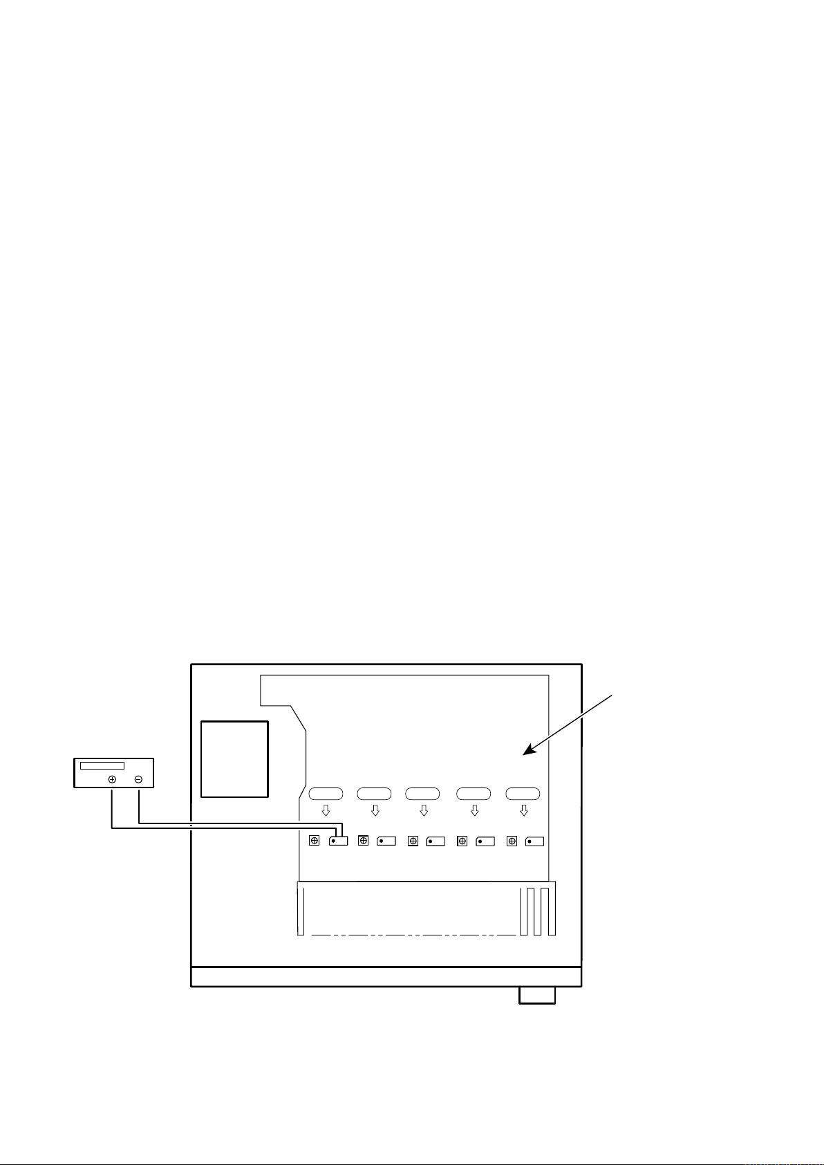
TECHNICAL SPECIFICATIONS for AVR-S500BT ...................9
DIMENSION ...............................................................................9
TECHNICAL SPECIFICATIONS for AVR-X510BT .................10
DIMENSION .............................................................................10
PRECAUTIONS DURING SERVICE .......................................11
Initializing This Unit .................................................................11
DISASSEMBLY ........................................................................12
1. FRONT PANEL ASSY ........................................................14
2. DIGITAL PCB .....................................................................15
3. RADIATOR ASSY ...............................................................16
4. SMPS PCB .........................................................................17
5. REGULATOR PCB .............................................................17
6. TRANS POWER ................................................................17
SPECIAL MODE ......................................................................18
Special mode setting button ....................................................18
1. Initialization Mode ..............................................................20
2. Version Display Mode ........................................................20
3. Change Video Format and Display Language Mode ........21
4. Product Mode .....................................................................22
PROCEDURE AFTER REPLACING THE
MICROPROCESSOR, ETC ....................................................26
Firmware Update Procedure ...................................................26
1. Updating by USB ................................................................26
ADJUSTMENT .........................................................................30
TROUBLE SHOOTING ............................................................33
1. POWER ..............................................................................33
2. Analog video ......................................................................34
3. HDMI/DVI ...........................................................................35
4. AUDIO ................................................................................40
5. Bluetooth ............................................................................42
6. SMPS .................................................................................43
CLOCK FLOW & WAVE FORM IN DIGITAL BLOCK .............46
ANALOG AUDIO BLOCK DIAGRAM .....................................47
DIGITAL AUDIO/HDMI BLOCK DIAGRAM .............................48
VIDEO BLOCK DIAGRAM ......................................................49
POWER BLOCK DIAGRAM ....................................................50
LEVEL DIAGRAM ....................................................................51
WIRING DIAGRAM ..................................................................55
PRINTED WIRING BOARDS ...................................................56
FRONT ....................................................................................56
DIGITAL ...................................................................................59
FRONT CABLE GUIDE ...........................................................61
SMPS .....................................................................................61
REGULATOR ..........................................................................63
TUNER ....................................................................................64
VIDEO .....................................................................................64
PHONE WIRE GUIDE .............................................................64
STANDBY ................................................................................64
PHONE ...................................................................................64
USB & MIC ..............................................................................64
(A SIDE) ..................................................................................64
SCHEMATIC DIAGRAMS (1/12) .............................................65
MCU ........................................................................................65
HDMI OSD ..............................................................................66
HDMI 4K ..................................................................................67
DSP .........................................................................................68
DIGITAL POWER ....................................................................69
INPUT VOLUME .....................................................................70
USB BT ...................................................................................71
VIDEO OPTICAL .....................................................................72
MAIN .......................................................................................73
FRONT ....................................................................................74
REGULATOR ..........................................................................75
SMPS ......................................................................................76
EXPLODED VIEW AVR-S500BT ............................................78
EXPLODED VIEW AVR-X510BT .............................................79
PACKING VIEW AVR-S500BT ................................................80
PACKING VIEW AVR-X510BT ................................................81
SEMICONDUCTORS ...............................................................82
1. IC's .....................................................................................82
2. FL DISPLAY .....................................................................108
2
Page 3
ABOUT THIS MANUAL
Read the following information before using the service manual.
What you can do with this manual
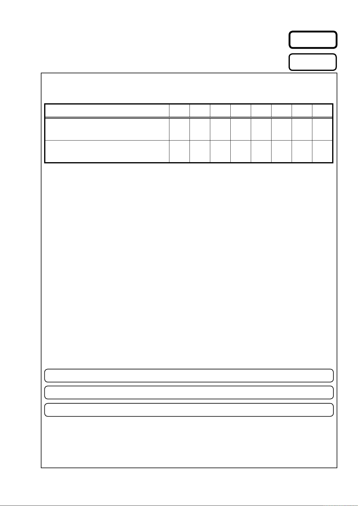
Search for a Ref. No. (phrase)
(Ctrl+Shift+F)
You can use the search function in Acrobat Reader to
search for a Ref. No. in schematic diagrams, printed
wiring circuit diagrams, block diagrams, and parts
lists.
1.Press Ctrl+Shift+Fonthekeyboard.
• The Search window appears.
F
Shift
Ctrl
2.EntertheRef.No.youwanttosearchforinthe
Search window, and then click the Search button.
•A list of search results appears.
Jump to the target of a schematic
diagram connector
Click the Ref. No. of the target connector in the red
box around a schematic diagram connector.
•The screen jumps to the target connector.
CP401
v
CP106
3.Click an item on the list.
• The screen jumps to the page for that item, and the
searchphraseisdisplayed.
•Pagemagnicationstaysthesameasbeforethe
jump.
3
Page 4
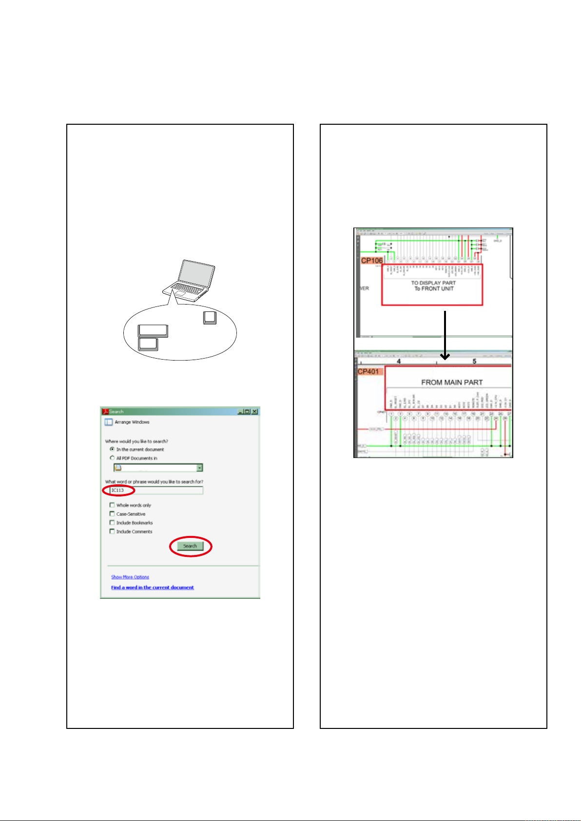
Using Adobe Reader (Windows version)
Add notes to this data (Sign)
TheSignfunctionletsyouaddnotestothedatain
this manual.
Savetheleonceyouhavenishedaddingnotes.
[Example using Adobe Reader X]
On the "View" menu, click "Sign".
• The Sign pane appears.
[Example using Adobe Reader 9]
On the "Document" menu, click "Sign".
Magnify schematic / printed circuit
board diagrams - 1
(Ctrl+Space, mouse operation)
Press Ctrl+Spaceonthekeyboardanddragthe
mousetoselecttheareayouwanttoview.
• Theselectedareaismagnied.
0
Ctrl Space
• Whenyouwanttomovetheareashown,hold
down Space and drag the mouse.
• Whenyouwanttoshowafullpageview,press
Ctrl+0onthekeyboard.
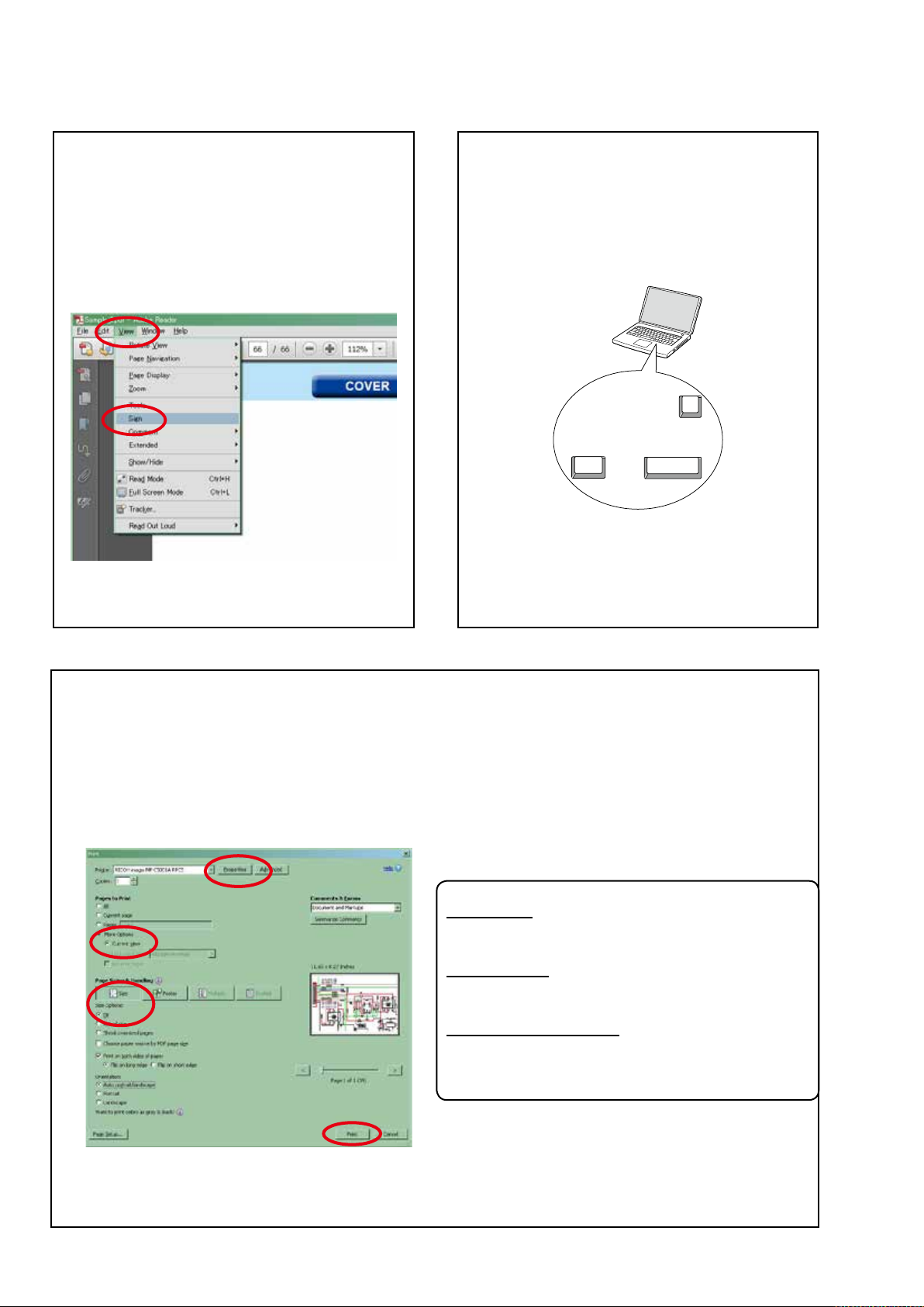
Print a magnied part of the manual
ThePropertiesdialogboxandfunctionswillvarydependingonyourprinter.
1. Dragthemousetomagnifythepartyouwanttoprint.
2. On the "File" menu, click "Print".
3. CongurethefollowingsettingsinthePrintdialogbox.
• Properties
Click this button and check that the printer is set to a
suitable paper size.
• Page to print
Select the following checkbox.
"More Options" : "Current View"
• Page Sizing & Handling
Select the following checkbox.
"Size" / "Size Options" : "Fit"
4. Click the Print button to start printing.
4
Page 5
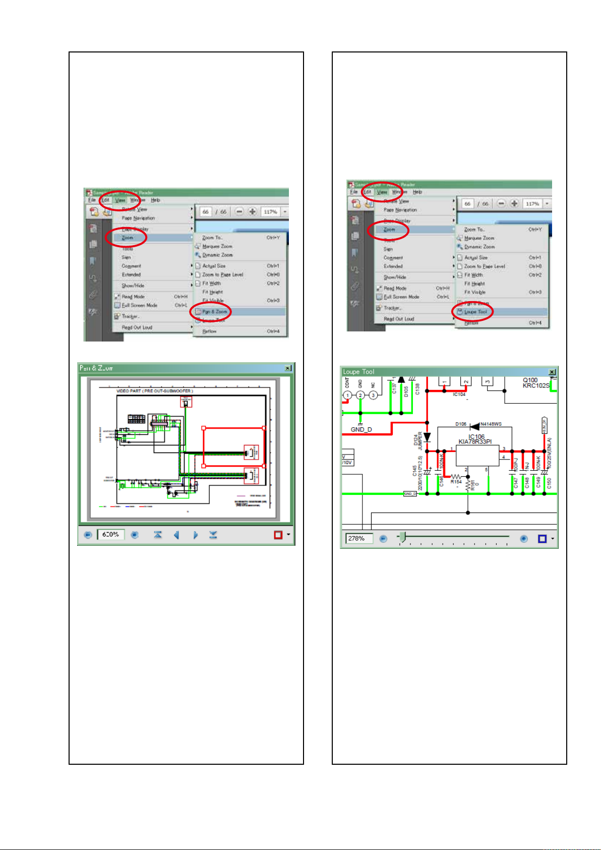
Magnify schematic / printed circuit
board diagrams - 2
(Pan & Zoom function)
ThePan&Zoomfunctionletsyouseewhichpartof
amagnieddiagramisbeingshowninaseparate
window.
[Example using Adobe Reader X]
On the "View" menu, point to "Zoom", and then click
"Pan & Zoom".
Magnify schematic / printed circuit
board diagrams - 3
(Loupe Tool function)
TheLoupeToolfunctionletsyoumagnifyaspecic
part of a diagram in a separate window.
[Example using Adobe Reader X]
On the "View" menu, point to "Zoom", and then click
"Loupe Tool".
• The Pan & Zoom window appears on the screen.
[Example using Adobe Reader 9]
On the "Tools" menu, point to "Select & Zoom", and
then click "Pan & Zoom Window".
• The Loupe Tool window appears on the screen.
[Example using Adobe Reader 9]
On the "Tools" menu, point to "Select & Zoom", and
then click "Loupe Tool Window".
5
Page 6

SAFETY PRECAUTIONS
The following items should be checked for continued protection of the customer and the service technician.
leakage current check
Beforereturningthesettothecustomer,besuretocarryouteither(1)aleakagecurrentcheckor(2)alinetochassis
resistance check. If the leakage current exceeds 0.5 milliamps, or if the resistance from chassis to either side of the
power cord is less than 460 kohms, the set is defective.
Be sure to test for leakage current with the AC plug in both polarities, in addition, when the set's power is in each state
(on,offandstandbymode),ifapplicable.
CAUTION
Please heed the following cautions and instructions during servicing and
inspection.
◎Heed the cautions!
Cautions which are delicate in particular for servicing
are labeled on the cabinets, the parts and the chassis,
etc. Be sure to heed these cautions and the cautions
described in the handling instructions.
◎Cautions concerning electric shock!
(1) AnACvoltageisimpressedonthisset,soifyou
touch internal metal parts when the set is energized,
youmaygetanelectricshock.Avoidgettingan
electricshock,byusinganisolatingtransformer
and wearing gloves when servicing while the set is
energized,orbyunpluggingthepowercordwhen
replacing parts, for example.
(2) Therearehighvoltagepartsinside.Handlewith
extra care when the set is energized.
◎ Caution concerning disassembly and
assembly!
Through great care is taken when parts were
manufacturedfromsheetmetal,theremaybeburrson
theedgesofparts.Theburrscouldcauseinjuryifngers
are moved across them in some rare cases. Wear gloves
toprotectyourhands.
◎Use only designated parts!
Theset'spartshavespecicsafetyproperties(re
resistance,voltageresistance,etc.).Besuretouseparts
which have the same properties for replacement. The
burrs have the same properties. In particular, for the
importantsafetypartsthatareindicatedbythez mark
on schematic diagrams and parts lists, be sure to use
the designated parts.
◎ Be sure to mount parts and arrange the wires
as they were originally placed!
Forsafetyseasons,somepartsusetapes,tubesorother
insulatingmaterials,andsomepartsaremountedaway
from the surface of printed circuit boards. Care is also
takenwiththepositionsofthewiresbyarrangingthem
andusingclampstokeepthemawayfromheatingand
highvoltageparts,sobesuretoseteverythingbackas
itwasoriginallyplaced.
◎Make a safety check after servicing!
Check that all screws, parts and wires removed or
disconnected when servicing have been put back in their
original positions, check that no serviced parts have
deteriorate the area around. Then make an insulation
check on the external metal connectors and between
the blades of the power plug, and otherwise check that
safetyisensured.
(Insulationcheckprocedure)
Unplug the power cord from the power outlet, disconnect
the antenna, plugs, etc., and on the power. Using a 500V
insulation resistance tester, check that the insulation
resistancevaluebetweentheinplugandtheexternally
exposedmetalparts(antennaterminal,headphones
terminal,inputterminal,etc.)is1MΩorgreater.Ifitis
less, the set must be inspected and repaired.
CAUTION
Concerning important
safety parts
Manyoftheelectricandthestructuralpartsusedinthe
sethavespecialsafetyproperties.Inmostcasesthese
propertiesaredifculttodistinguishbysight,andtheuse
ofreplacementpartswithhigherratings(ratedpower
andwithstandvoltage)doesnotnecessarilyguarantee
thatsafetyperformancewillbepreserved.Partswith
safetypropertiesareindicatedasshownbelowonthe
wiring diagrams and the parts list in this service manual.
Be sure to replace them with the parts which have the
designated part number.
(1) Schematicdiagrams .......Indicatedbythez mark.
(2) Partslists .......Indicatedbythez mark.
The use of parts other than the
designated parts could cause electric
shocks,resorotherdangerous
situations.
6
Page 7
NOTE FOR SCHEMATIC DIAGRAM
WARNING:
Partsindicatedbythezmarkhavecriticalcharacteristics.UseONLYreplacementpartsrecommendedbythemanufacturer.
CAUTION:
Beforereturningthesettothecustomer,besuretocarryouteither(1)aleakagecurrentcheckor(2)alinetochassisresistancecheck.
If the leakage current exceeds 0.5 milliamps, or if the resistance from chassis to either side of the power cord is less than 460 kohms, the
set is defective.
WARNING:
DONOTreturnthesettothecustomerunlesstheproblemisidentiedandremedied.
NOTICE:
ALLRESISTANCEVALUESINOHM.k=1,000OHM/M=1,000,000OHM
ALLCAPACITANCEVALUESAREEXPRESSEDINMICROFARAD,UNLESSOTHERWISEINDICATED.PINDICATESMICRO-MICRO
FARAD.EACHVOLTAGEANDCURRENTAREMEASUREDATNOSIGNALINPUTCONDITION.CIRCUITANDPARTSARESUBJECT
TOCHANGEWITHOUTPRIORNOTICE.
NOTE FOR PARTS LIST
1.Partsindicatedby"nsp" on this table cannot be supplied.
2.Whenorderingapart,makeacleardistinctionbetween"1"and"I"(i)toavoidmis-supplying.
3.Apartorderedwithoutspecifyingitspartnumbercannotbesupplied.
4.Partindicatedby"★" mark is not illustrated in the exploded view.
WARNING:
INSTRUCTIONS FOR HANDLING SEMI-CONDUCTORS AND OPTICAL UNIT
Electrostaticbreakdownofthesemi-conductorsoropticalpickupmayoccurduetoapotentialdifferencecausedby
electrostatic charge during unpacking or repair work.
Partsindicatedbythezmarkhavecriticalcharacteristics.UseONLYreplacementpartsrecommendedbythemanufacturer.
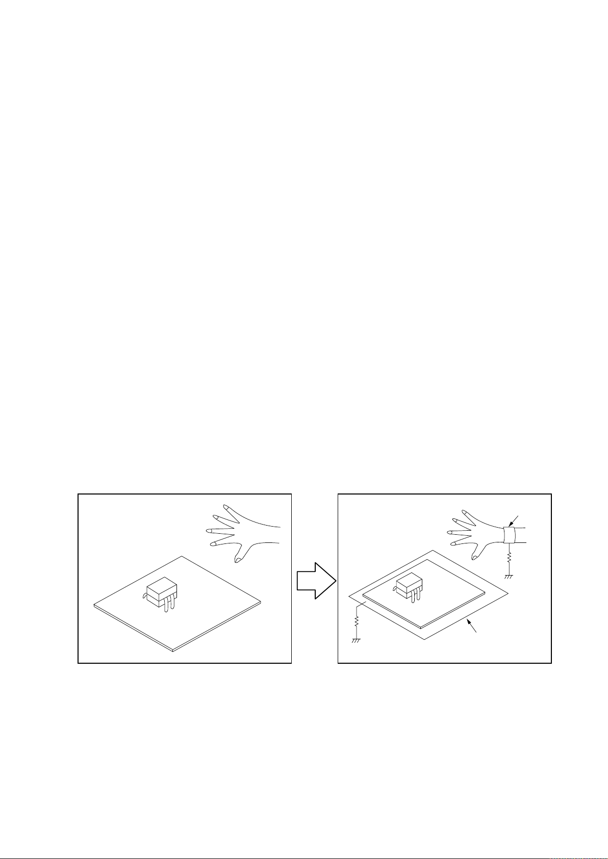
1. GroundforHumanBody
Besuretowearagroundingband(1MΩ)thatisproperlygroundedtoremoveanystaticelectricitythatmaybe
chargedonthebody.
2. GroundforWorkbench
Besuretoplaceaconductivesheetorcopperplatewithpropergrounding(1MΩ)ontheworkbenchorothersurface,
wherethesemi-conductorsaretobeplaced.Becausethestaticelectricitychargeonclothingwillnotescapethrough
thebodygroundingband,becarefultoavoidcontactingsemi-conductorswithyourclothing
<Incorrect>
<Correct>
CBA
CBA
1MΩ
Grounding Band
1MΩ
Conductive Sheet or
Copper Plate
7
Page 8

Personal notes:
8
Page 9

TECHNICAL SPECIFICATIONS FOR AVR-S500BT
nAudio Section
• Power amplifier
Rated output :
Front :
70 W + 70 W (8 Ω/ohms, 20 Hz – 20 kHz with 0.08 % T.H.D.)
90 W + 90 W (6 Ω/ohms, 1 kHz with 0.7 % T.H.D.)
Center :
70 W (8 Ω/ohms, 20 Hz – 20 kHz with 0.08 % T.H.D.)
90 W (6 Ω/ohms, 1 kHz with 0.7 % T.H.D.)
Surround :
70 W + 70 W (8 Ω/ohms, 20 Hz – 20 kHz with 0.08 % T.H.D.)
90 W + 90 W (6 Ω/ohms, 1 kHz with 0.7 % T.H.D.)
Output connectors : 6 – 16 Ω/ohms
• Analog
Input sensitivity/Input impedance : 200 mV/47 kΩ
Frequency response: 10 Hz – 100 kHz — +1, –3 dB (Direct mode)
S/N : 98 dB (IHF–A weighted, Direct mode)
nTuner section
[FM](Note: μV at 75 Ω, 0 dBf = 1 x 10
Reception frequency range :
(for E3) : [FM] 87.5 MHz – 107.9 MHz [AM]520 kHz – 1710 kHz
(for E1C) : [FM] 87.5 MHz – 108.0 MHz [AM]522 kHz – 1611 kHz
Effective sensitivity :
[FM]1.2 μV (12.8 dBf) [AM]18 μV
50 dB sensitivity :
[FM]MONO 2.8 μV (20.2 dBf)
S/N ratio :
[FM]MONO 70 dB (IHF–A weighted, Direct mode)
STEREO 67 dB (IHF–A weighted, Direct mode)
Distortion (at 1 kHz) :
[FM]MONO 0.7 %
STEREO 1.0 %
–15
W)
nBluetooth Section
Communications system : Bluetooth Version 2.1 + EDR
Transmission power : Maximum 2.5 mW (Class 2)
Maximum communication range : Approx. 32.8 ft/10m 2 in line of
sight
Frequency band : 2.4 GHz band
Modulation scheme : FHSS (Frequency-Hopping Spread Spectrum)
Supported proles : A2DP (Advanced Audio Distribution Prole)1.2
Corresponding codec : SBC, AAC
Transmission range (A2DP) : 20 Hz - 20,000 Hz
nGeneral
Power supply : (for E3) : AC 120 V, 60 Hz
(for E1C) : AC 220 V, 50 Hz
Power consumption :310W
Power consumption in standby mode: 0.1 W
Power consumption in CEC standby mode: 0.5W
Power consumption when Bluetooth standby is used: 1W
(Enhanced Data Rate)
AVRCP (Audio Video Remote Control Prole)1.4
DIMENSION
Unit : in. (mm) Weight : 16 lbs 9 oz (7.5 kg)
17 3/32 (434)
(12)
15/32
12 9/16 (319)
11 11/32 (288)
3/4
(19)
(47)
1 27/32
7 3/4 (197)
(44)
1 47/64
5 23/64 (136)
5 15/16 (151)
2 23/64
(60)
1 49/64 (45) 1 49/64 (45)
13 35/64 (344)
(15)
19/32
9
Page 10
TECHNICAL SPECIFICATIONS FOR AVR-X510BT
nAudio Section
• Power amplifier
Rated output :
Front :
70 W + 70 W (8 Ω/ohms, 20 Hz – 20 kHz with 0.08 % T.H.D.)
90 W + 90 W (6 Ω/ohms, 1 kHz with 0.7 % T.H.D.)
Center :
70 W (8 Ω/ohms, 20 Hz – 20 kHz with 0.08 % T.H.D.)
90 W (6 Ω/ohms, 1 kHz with 0.7 % T.H.D.)
Surround :
70 W + 70 W (8 Ω/ohms, 20 Hz – 20 kHz with 0.08 % T.H.D.)
90 W + 90 W (6 Ω/ohms, 1 kHz with 0.7 % T.H.D.)
Output connectors : 6 – 16 Ω/ohms
• Analog
Input sensitivity/Input impedance : 200 mV/47 kΩ
Frequency response: 10 Hz – 100 kHz — +1, –3 dB (Direct mode)
S/N : 98 dB (IHF–A weighted, Direct mode)
nTuner section
[FM](Note: μV at 75 Ω, 0 dBf = 1 x 10
Reception frequency range (for E1 / E1C) :
[FM] 87.5 MHz – 108.0 MHz [AM]522 kHz – 1611 kHz
Effective sensitivity :
[FM]1.2 μV (12.8 dBf) [AM]18 μV
50 dB sensitivity :
[FM]MONO 2.8 μV (20.2 dBf)
S/N ratio:
[FM]MONO 70 dB (IHF–A weighted, Direct mode)
STEREO 67 dB (IHF–A weighted, Direct mode)
Distortion (at 1 kHz) :
[FM]MONO 0.7 %
STEREO 1.0 %
–15
W)
nBluetooth Section
Communications system : Bluetooth Version 2.1 + EDR
Transmission power : Maximum 2.5 mW (Class 2)
Maximum communication range : Approx. 10m 2 in line of sight
Frequency band : 2.4 GHz band
Modulation scheme : FHSS (Frequency-Hopping Spread Spectrum)
Supported proles : A2DP (Advanced Audio Distribution Prole)1.2
Corresponding codec : SBC, AAC
Transmission range (A2DP) : 20 Hz - 20,000 Hz
nGeneral
Power supply : (for E1) : AC 230 V, 50 Hz / 60Hz
(for E1C) : AC 220 V, 50 Hz
Power consumption :310W
Power consumption in standby mode: 0.1 W
Power consumption in CEC standby mode: 0.5W
Power consumption when Bluetooth standby is used: 1W
(Enhanced Data Rate)
AVRCP (Audio Video Remote Control Prole)1.4
DIMENSION
Unit : in. (mm) Weight : 16 lbs 9 oz (7.5 kg)
17 3/32 (434)
(12)
15/32
12 9/16 (319)
11 11/32 (288)
3/4
(19)
(47)
1 27/32
7 3/4 (197)
(44)
1 47/64
5 23/64 (136)
2 23/64
(60)
1 49/64 (45) 1 49/64 (45)
13 35/64 (344)
(15)
19/32
10
5 15/16 (151)
Page 11
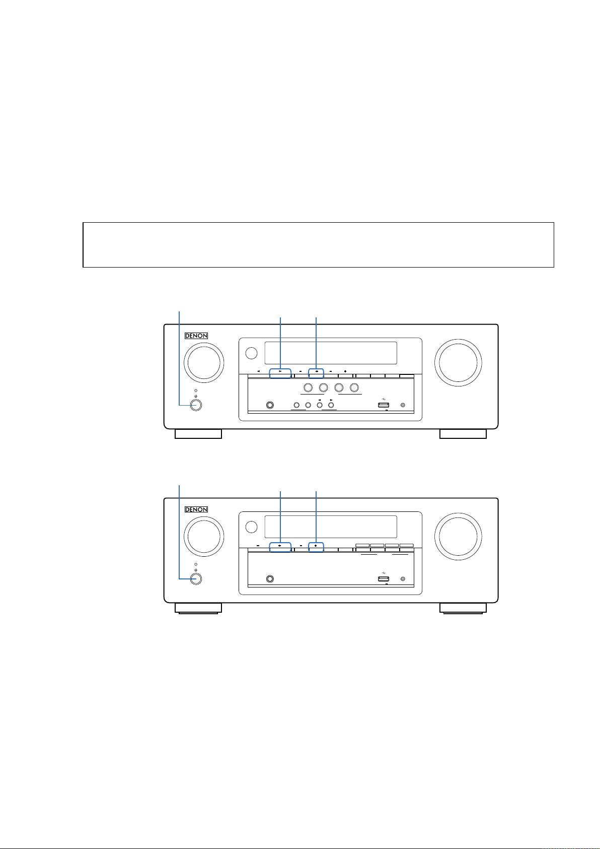
PRECAUTIONS DURING SERVICE
Initializing This Unit
Initialize this unit if you have replaced the microcomputer, one of the parts around the microcomputer, or the digital PCB.
1. Press the power button (X) to turn off the power.
2. AVR-S500BT: Hold down buttons "SOUND MODE 1" and "PRESET +" at the same time and press the power button
to turn on the power.
AVR-X510BT: Hold down buttons "PRESET +" and "TUNE +" at the same time and press the power button to turn on
the power.
3. Releasethebuttonsafterconrmingthatthedisplayashesinintervalsofapproximately1second.
The unit is initialized.
NOTE: • If the status in step 3 does not occur, start again from step 1.
•Initializingthedevicerestoressettingsconguredbytheusertothefactorysettings.
Takenoteofyoursettingsbeforehandandrecongurethemafterinitialization.
[AVR-S500BT]
[AVR-X510BT]
X
SOURCE SELECT
X
SOURCE SELECT
SOUND MODE 1
SOUND MODE
PRESET +
TUNER
PRESET CH
ON / OFF
PRESET +
TUNER
PRESET CH
CBL/SAT
2
1
BASS /
TREBLE
TONE CONTROL
TUNE +
TUNE
DVD/Blu-ray
ADJUST
TUNE
GAME
3
QUICK SELECT
DIMMER S TATUS
BAND MODE DIMMER STATUS
Bluetooth
4
DVD/Blu-ray
2
QUICK SELECT
MASTER VOLUME
SETUP MICPHONES
5V/1A
MASTER VOLUME
Bluetooth
GAMECBL/SAT
31
4
SETUP MICPHONES
5V/1A
11
Page 12
DISASSEMBLY
• Remove each part in the order of the arrows below.
• Reassemble removed parts in the reverse order.
• Read“ SAFETY PRECAUTION” before reassembling removed parts.
• If wire bundles are removed or moved during adjustment or part replacement, reshape the wires after completing the
work. Failure to shape the wires correctly may cause problems such as noise.
TOP CABINET
FRONT PANEL ASSY
See "DISASSEMBLY
1. FRONT PANEL ASSY"
and "EXPLODED VIEW"
FRONT PCB
(Ref. No. of EXPLODED VIEW : P1)
STANDBY PCB
(Ref. No. of EXPLODED VIEW : P2)
PHONE PCB
(Ref. No. of EXPLODED VIEW : P3)
USB & MIC PCB
(Ref. No. of EXPLODED VIEW : P4)
MODULE BLUETOOTH
(Ref. No. of EXPLODED VIEW : P5)
DIGITAL PCB
See "DISASSEMBLY
2. DIGITAL PCB ASSY"
and "EXPLODED VIEW"
VIDEO PCB
(Ref. No. of EXPLODED VIEW : P10)
DIGITAL PCB
(Ref. No. of EXPLODED VIEW : P8)
TUNER PCB
(Ref. No. of EXPLODED VIEW : P9)
RADIATOR ASSY
See "DISASSEMBLY
3. RADIATOR ASSY"
and "EXPLODED VIEW"
MAIN PCB
(Ref. No. of EXPLODED VIEW : P6)
SMPS PCB
See "DISASSEMBLY
4. SMPS PCB
and "EXPLODED VIEW"
SMPS PCB
(Ref. No. of EXPLODED VIEW : P12)
REGULATOR PCB
See "DISASSEMBLY
5. REGULATOR PCB"
and "EXPLODED VIEW"
REGULATOR PCB
(Ref. No. of EXPLODED VIEW : P11)
TRANS POWER
See "DISASSEMBLY
6. TRANS POWER"
and "EXPLODED VIEW"
TRANS POWER
(Ref. No. of EXPLODED VIEW : P15 )
12
Page 13
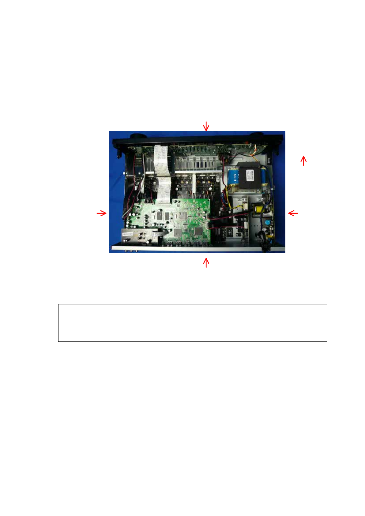
Explanatory Photos for“ DISASSEMBLY”
• The angles from which the photos are taken are shown by“ Photo angle: A, B, C, D“ .
• See the diagram below about the shooting direction of each photograph.
• Photographs with no shooting direction indicated were taken from the top of the set.
• The photograph is AVR-S500BT E3 model.
The viewpoint of each photograph
(Shooting direction)
Shooting direction: B
Front side
Shooting direction: C
Shooting direction: A
Note: • Before disassembling this unit, be sure to discharge the power line (the colored line in the
schematic diagram).
• FFC cables with one end disconnected should be insulated by using tapes, etc.
Shooting direction: D
13
Page 14
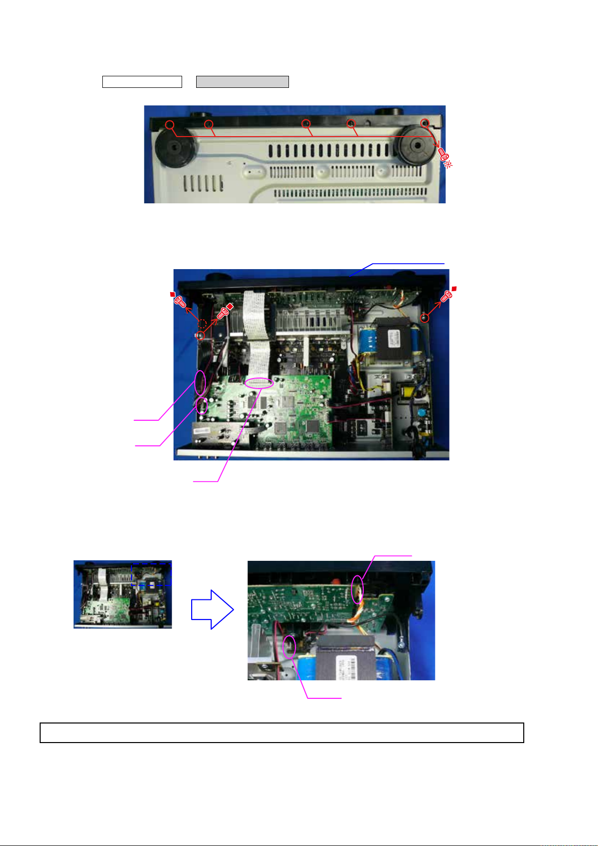
1. FRONT PANEL ASSY
Proceeding : CABINET TOP
(1) Remove the screws.
View from the bottom
(2) Remove the screws and disconnect the FFC.
FRONT PANEL ASSY
→
FRONT PANEL ASSY
CN713
CN752
(3) Disconnect the connector wires.
FFC
CN102
CN104
See "EXPLODED VIEW" for the disassembly method of each PCB included in FRONT PANEL ASSY.
14
Page 15
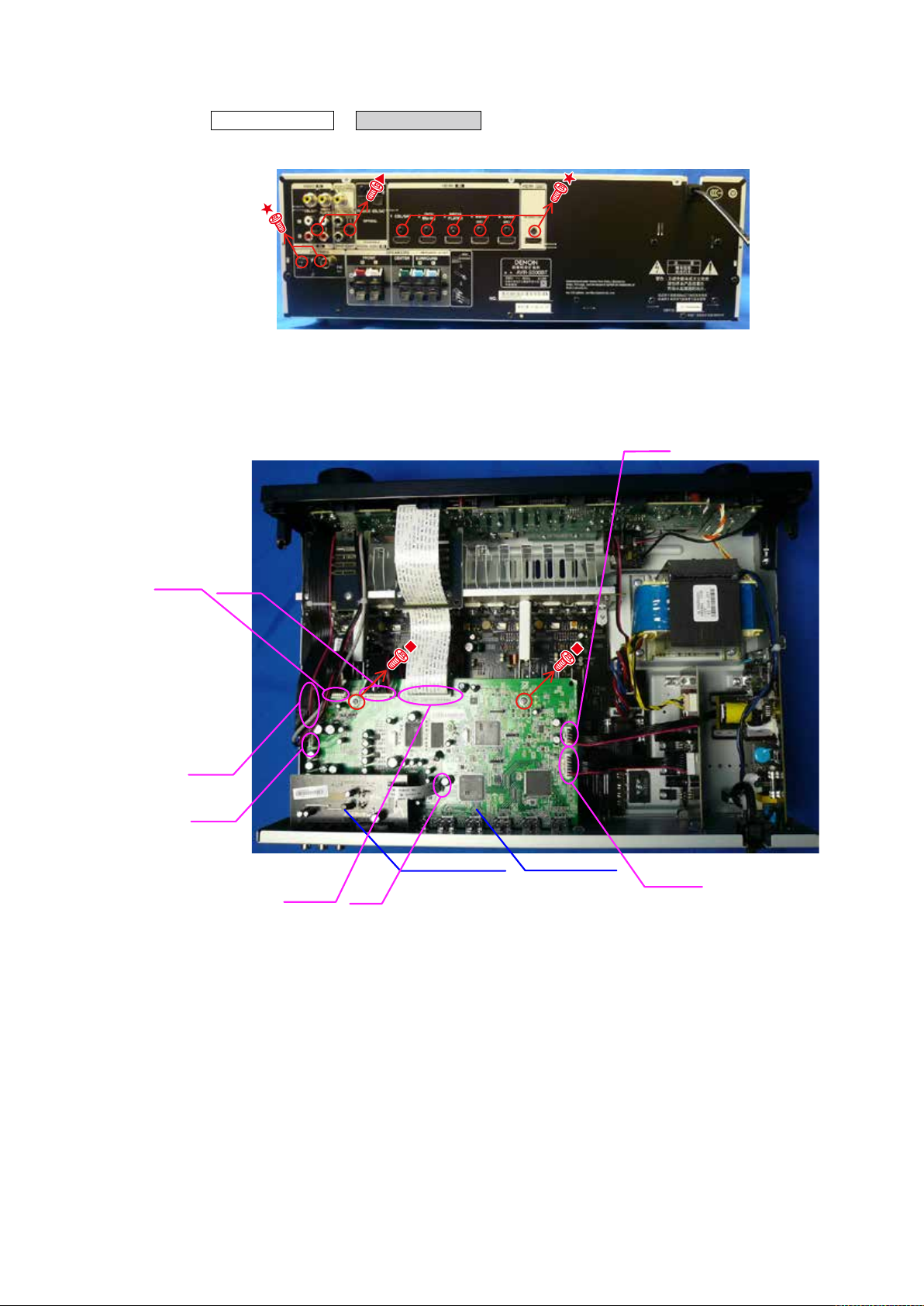
2. DIGITAL PCB
Proceeding : CABINET TOP
(1) Remove the screws.
Shooting direction: A
(2) Remove the screws.
Disconnect the connector wires and FFC.
DIGITAL PCB
→
CN751
CN712
CN713
CN752
CN772
FFC
VIDEO/OPT PCB
FFC
DIGITAL PCB
CN771
15
Page 16
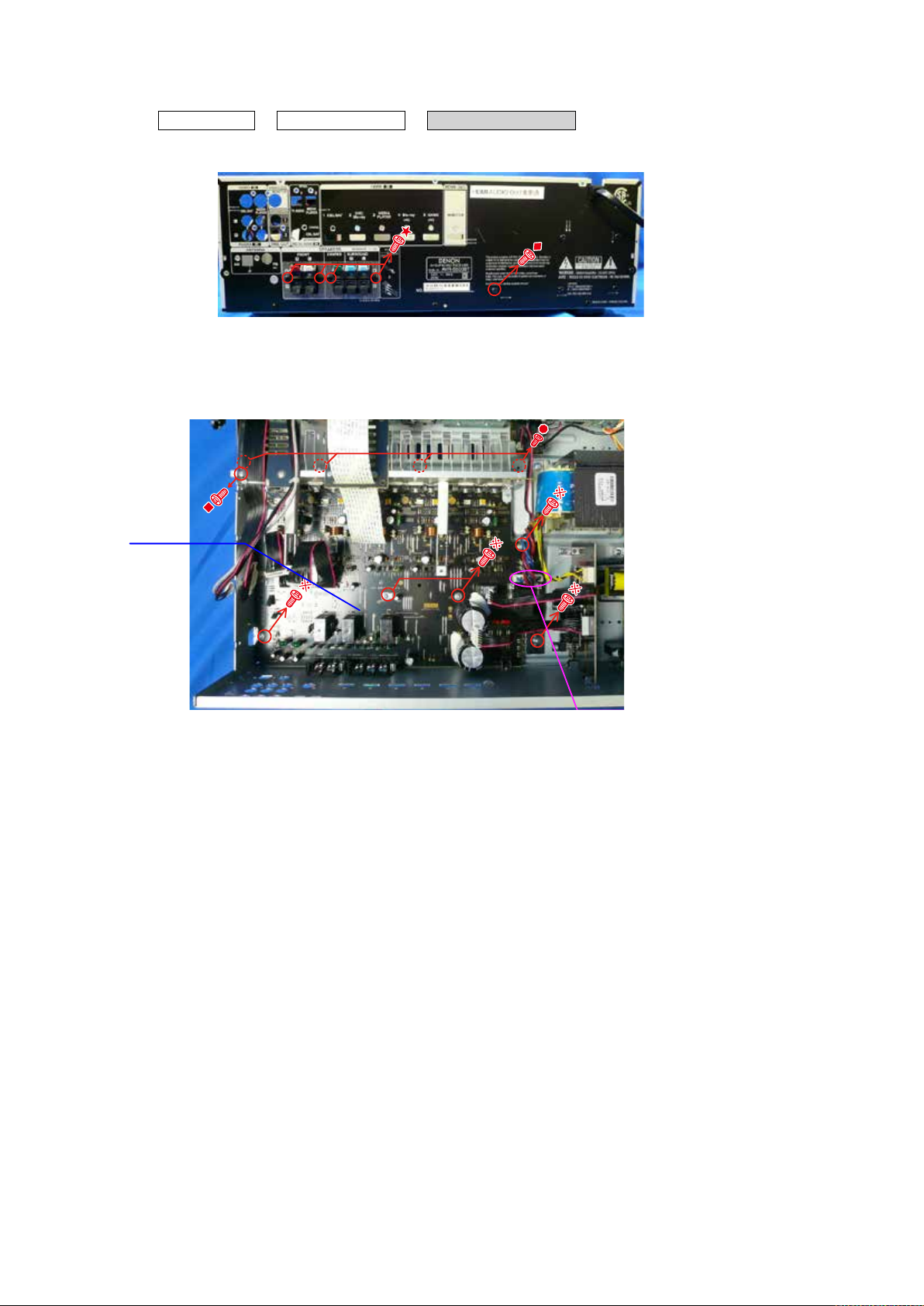
3. RADIATOR ASSY
CN503
Proceeding : TOP COVER
(1) Remove the screws.
Shooting direction: A
(2) Remove the screws then disconnect the connector wire.
Remove the RADIATOR ASSY from the CHASSIS BOTTOM.
MAIN PCB
DIGITAL PCB
→
→
RADIATOR ASSY
16
Page 17
4. SMPS PCB
Proceeding : CABINET TOP
See "EXPLODED VIEW" for the disassembly method of SMPS PCB.
→
SMPS PCB
5. REGULATOR PCB
Proceeding : CABINET TOP
See "EXPLODED VIEW" for the disassembly method of REGULATOR PCB.
REGULATOR PCB
→
6. TRANS POWER
Proceeding : CABINET TOP
See "EXPLODED VIEW" for the disassembly method of TRANS POWER.
TRANS POWER
→
17
Page 18
SPECIAL MODE
Special mode setting button
No. 1, 2 : Hold down buttons A and B at the same time and press the power button (
b
No. 3, 4 : Hold down buttons A, B and C for at least 3 seconds while the power is on.
AVR-S500BT
Mode Button A Button B Button C Contents
1 Initialization SOUND MODE
1
PRESET +
2 Version Display PRESET + TUNE -
Chang Video Format
3
and Display Languge
4 Product Mode SOUND MODE
PRESET
-
PRESET + TUNE -
PRESET
1
PRESET
-
Backup data initialization is carried out.
(See 11 page.)
Firmware versions such as Main, DSP or OSD
are displayed in the FL display. Errors are
displayed or when they occur.
(See 20 page.)
Select the mode shown below.
"Remote Lock", "Tuning Step Change", "OSD
+
Update", "Protection History Display" and "Mic
Mode".
)
to turn on the power.
X
X
SOURCE SELECT
SOUND MODE 1
SOUND MODE
PRESET -, +
TUNER
PRESET CH
CBL/SAT
1
BASS /
ON / OFF
TREBLE
TONE CONTROL
TUNE-
DVD/Blu-ray
2
ADJUST
QUICK SELECT
TUNE
GAME
3
4
MASTER VOLUME
BAND MODE DIMMER STATUS
Bluetooth
SETUP MICPHONES
5V/1A
18
Page 19
No. 1, 2 : Hold down buttons A and B at the same time and press the power button (
b
No. 3, 4 : Hold down buttons A, B and C for at least 3 seconds while the power is on.
AVR-X510BT
Mode Button A Button B Button C Contents
1 Initialization PRESET + TUNE +
2 Version Display TUNE + DIMMER
Chang Video Format
3
and Display Languge
TUNE - TUNE + DIMMER
4 Product Mode PRESET + TUNE - TUNE +
Backup data initialization is carried out.
(See 11 page.)
Firmware versions such as Main, DSP or OSD
are displayed in the FL display. Errors are
displayed or when they occur.
(See 20 page.)
Select the mode shown below.
"Remote Lock", "Tuning Step Change", "OSD
Update", "Protection History Display" and "Mic
Mode".
)
to turn on the power.
X
X
SOURCE SELECT
PRESET +
TUNER
PRESET CH
TUNE -, +
TUNE
DIMMER
DIMMER STATUS
MASTER VOLUME
Bluetooth
GAMECBL/SAT
DVD/Blu-ray
31
2
4
QUICK SELECT
SETUP MICPHONES
5V/1A
19
Page 20
1. Initialization Mode
1.1. Operations
Hold down buttons below at the same time and press the power button to turn on the power.
"SOUND MODE 1", "PRESET +" (AVR-S500BT)
"PRESET +", "TUNE +" (AVR-X510BT)
Release the buttons after conrming that the display ashes in intervals of approximately 1 second.
1.2. Actions
Initialize this unit.
Note:Settings for the tuner step are not initialized.
2. Version Display Mode
2.1. Operations
Hold down buttons below at the same time and press the power button to turn on the power.
"PRESET +", "TUNE -" (AVR-S500BT)
"TUNE +", "DIMMER" (AVR-X510BT)
Press the button "STATUS" to display the versions.
2.2. Actions
Press the "STATUS" button to display the versions in the following order.
Error information(See 2.4. Error display) →q Model destination information → w Main-µcom version → e Main IAP →
DSP version →
r
When an error has occurred in this unit, the error information is displayed initially when entering this mode. (5 seconds)
OSD version
t
→
USB version
y
→ Nomal display
Display State
Model destination information
q
AVR-S500BT
AVR-X510BT E1 model
AVR-X510BT E1C model
AVR-S500BT E1C model
Main-µcom version
w
Main IAP
e
DSP version
r
OSD version
t
USB version
y
E3 model
A V R - S 5 0 0 E 3
A V R - X 5 1 0 E 1
A V R - X 5 1 0 E 1 C
A V R - S 5 0 0 E 1 C
M a i n . * * * * - V * . * *
M a i n I A P V * * . * *
D S P . * . * . *
O S D : * * . * *
U S B . * * . * * . * *
2.3. Canceling the mode:
Press the X button to turn the power off.
2.4. Error display
See the following table for each "Error information" display and its contents (status).
Condition - State
DSP NG When DSP boot, executing DSP reset makes to becomes error.
DSP OK (No error display, version display only)
20
D S P E R R O R 0 1
Page 21
3. Change Video Format and Display Language Mode
3.1. Operations
Hold down buttons below for at least 3 seconds while the power is on.
"PRESET -", "PRESET +", "TUNE -" (AVR-S500BT)
"TUNE -", "TUNE +", "DIMMER" (AVR-X510BT)
Note: Do not start in this mode when displaying the OSD MENU using the MENU button.
3.2. Actions
This unit is in VIDEO Format at startup.
Press the button below to switch between Video Format and Display Language.
"TUNE +" AVR-S500BT
"STATUS" AVR-X510BT
3.2.1. Video Format
Press the button below to switch between NTSC and PAL.
"PRESET +" or "TUNE -" AVR-S500BT
"PRESET +" or "DIMMER" AVR-X510BT
FLD
V . F o r m a t : < N T S C >
↓↑
FLD
V . F o r m a t : < P A L >
↓↑
Return to top.
Press the "Preset -" button to set format. The display then return to the normal mode.
3.2.1.Language
Press the button below to switch display language.
"PRESET +" or "TUNE -" AVR-S500BT
"PRESET +" or "DIMMER" AVR-X510BT
FLD
L a n g . : < E N G L I S H >
↓↑
FLD
L a n g . : < S P A N I S H >
↓↑
FLD
L a n g . : < F R E N C H >
↓↑
FLD
L a n g . : < C H I N E S E >
↓↑
Return to top.
Press the "Preset -" button to set display language. The display then return to the normal mode.
21
Page 22
4. Product Mode
Select "Remote Lock", "Tuner Step", "OSD update", "Protection History Display" or "Mic Mode" .
4.1. Operations
Hold down buttons below for at least 3 seconds while the power is on.
"SOUND MODE1", "PRESET -", "PRESET +" (AVR-S500BT)
"PRESET +", "TUNE -", "TUNE +" (AVR-X510BT)
Each mode shown on the display changes each time the button below is pressed.
"TUNE +" (AVR-S500BT)
"STATUS" (AVR-X510BT)
Press the buttons below to switch the display "On"/"Off".
"PRESET +", "TUNE -" (AVR-S500BT)
"PRESET +", "DIMMER" (AVR-X510BT)
Press the button below to set the displayed "On"/"Off".
"PRESET -" (AVR-S500BT)
"TUNE -" (AVR-X510BT)
4.2. Displaying and Selecting Each Mode
Remote Lock Mode
FLD
R E M O T E L O C K : O f f
Press the "TUNE +"(AVR-S500BT) button.
Press the "STATUS"(AVR-X510BT) button.
Tuner Step Change Mode
FLD
T U N E R : A M 9 / F M 5 0
OSD Update Mode
FLD
O S D U p d a t e : O f f
Protection History Display Mode
FLD
N O P R O T E C T
Mic Mode
FLD
M I C M o d e
Return to top.
4.3. Canceling Each Mode
See the actions of each mode.
Press the "TUNE +"(AVR-S500BT) button.
Press the "STATUS"(AVR-X510BT) button.
Press the "TUNE +"(AVR-S500BT) button.
Press the "STATUS"(AVR-X510BT) button.
Press the "TUNE +"(AVR-S500BT) button.
Press the "STATUS"(AVR-X510BT) button.
Press the "TUNE +"(AVR-S500BT) button.
Press the "STATUS"(AVR-X510BT) button.
22
Page 23
4.4.1. Remote Lock Mode
To enter the Product Mode, to display the Remote Lock Mode.
Press the button below to switch between On and Off.
"PRESET +" / "TUNE -" (AVR-S500BT)
"PRESET +" / "DIMMER" (AVR-X510BT)
FLD
R E M O T E L O C K : O f f
↓↑
FLD
R E M O T E L O C K : O n
Press the button below to set On/Off. The display then return to the normal mode.
"PRESET -" (AVR-S500BT)
"TUNE -" (AVR-X510BT)
4.4.2. Tuner Step Change Mode
To enter the Product Mode, to display the Tuner Step Change mode.
Press the button below to switch between AM9/FM50 and AM10/FM200.
"PRESET +" / "TUNE -" (AVR-S500BT)
"PRESET +" / "DIMMER" (AVR-X510BT)
FLD
R E M O T E L O C K : O f f
↓↑
FLD
R E M O T E L O C K : O n
Press the button below to set On/Off. The display then return to the normal mode.
"PRESET -" (AVR-S500BT)
"TUNE -" (AVR-X510BT)
To operate this unit in the set step, either remove the power plug from the power outlet or press the power button to turn off
the power, and then turn the power on again.
*The initialization will not initialize the tuner step frequency.
4.4.3. OSD Update Mode
Not for service. Do not operate.
Cancellation of the mode
Disconnect the AC plug of this unit to turn the power off.
23
Page 24
4.4.4. Protection History Display Mode
To enter the Product Mode, to display the Protection History Display Mode.
(1) If no protections have occurred.
FLD
N O P R O T E C T
(2) For THERMAL (when the last protection incident was THERMAL(A) or THERMAL(B) protection)
FLD
P R T : T H E R M A L A
FLD
P R T : T H E R M A L B
Cause: The temperature of the heat sink is excessive.
If the power is turned on without correcting the abnormality, the protection function will work about 4 minutes later
and the power supply will be shut off.
(3) For ASO (when the last protection incident was ASO protection)
FLD
P R T : A S O
Cause: The line between speaker terminals is shorted, or speakers with impedance of less than the rated value.
Supplementary information: As the excess current is detected after operation of the speaker relay, a short on the
speaker terminal and the connected speaker can be identied.
(4) For DC (when the last protection incident was DC protection)
FLD
P R T : D C
Cause: DC output of the power amplier is abnormal.
If the power is turned on without correcting the abnormality, the protection function will work about 6 seconds later
and the power supply will be shut off.
(5) For Power(when the last protection incident was Power protection)
FLD
P R T : P o w e r
Cause: The Power Supply(±12V) is abnormal.
Additional causes of protection can be due to loose connections, associated components, Microprocessor, etc.
b
Press the button below to set On/Off. The display then return to the normal mode.
"PRESET -" (AVR-S500BT)
"TUNE -" (AVR-X510BT)
Clearing the protection history
There are two ways to clear the protection history, as described below.
(1) Start up the set in error (protection display) mode and display the error, then press and hold down the below button for
3 seconds.
FLD
P R T : D C
Press the button for 3 seconds.
FLD
P R T : C L E A R
FLD
N O P R O T E C T
(2) Initialize. ( 20 page.)
The above is displayed and the protection history is cleared.
24
Page 25

4.4.5. Mic Mode
Not for service. Do not operate.
Cancellation of the mode
Press the power button to turn off the power or disconnect the AC plug of this unit to turn the power off.
25
Page 26
PROCEDURE AFTER REPLACING THE MICROPROCESSOR, ETC
The procedure after replacing the u-COM (Microprocessor), ash ROM, etc. is as follows.
PCB Name Ref. No. Description
Digital IC711 STM32F101ZG B SOFTWARE: Main
Digital
Digital
IC722 MX25L3206EM2I-12G B SOFTWARE: GUI ROM
IC742 MX25L8006EM2I-12G B SOFTWARE: DSP ROM
After replacing
A : The software has been written. The software is not written at the time of replacement.
B : The software has been written. The software may need to be rewritten by version updates. Check the version.
C : The software has not been written. The software needs to be written after replacement. See “Firmware Update
Procedure” for information on writing the software.
D : The software has been written. Be sure to rewrite with the latest software for your service region. See “Firmware Update
Procedure” for information on writing the software.
Firmware Update Procedure
1. Updating by USB
The latest rmware can be downloaded to a USB Memory for updates.
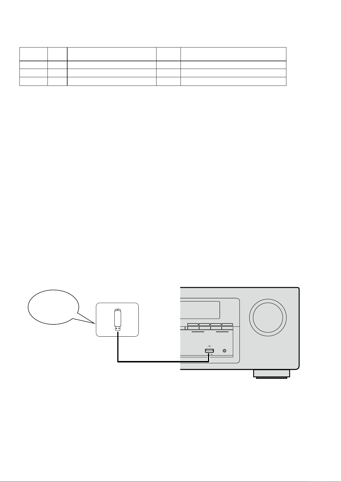
1.1. Connecting to the USB Memory
(1) Prepared
• USB format: Prepare a USB memory formatted in FAT16 or FAT32.
• Do not run the USB memory through a hub.
• Do not connect a computer to the USB port of this unit using a USB cable.
• Do not use an extension cable when connecting the USB memory.
After
replaced
Remark
1.2. Unzip Download File
Unzip the downloaded le on your computer.
You can nd "S500BT_USB_V**_**.fw" fole after unzipped. Copy that le to USB ash drive.
You have to put "S500BT_USB_V**_**.fw" le on root directly on USB ash drive(memory).
1.3. Insert the USB memory device in the USB port
Download the
firmware to a USB
memory.
CBL/SAT
S
2
DVD/Blu-ray
QUICK SELECT
5V/1A
Bluetooth
GAME
31
4
SETUP MIC
MASTER VOLUME
26
Page 27
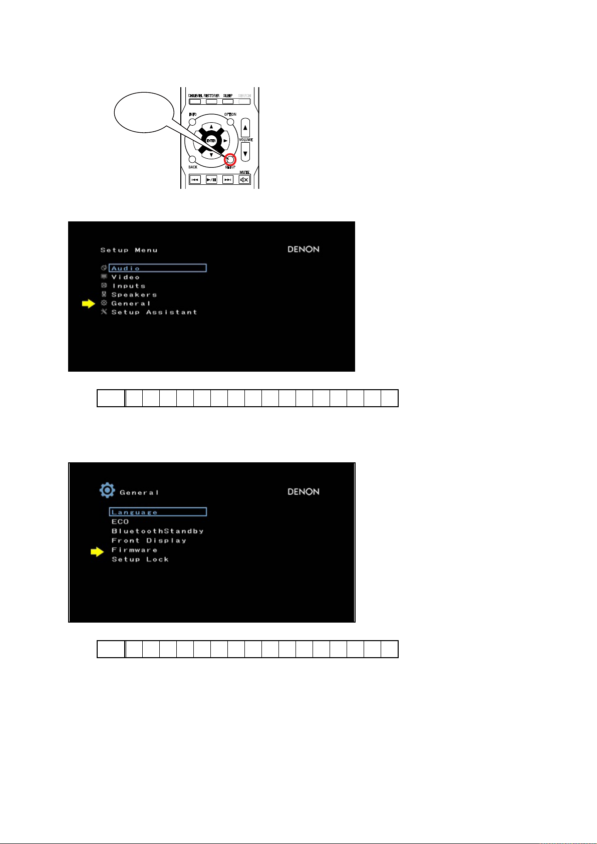
1.5. Start the update
TV AUDIO
QUICK SELECT
POWER
MODE
AM
MEMORY
CHANNEL
TUNE
FMCBL/SAT
Blu-ray
GAME
Bluetooth
USB
ECO
21 3 4
Turn on the power of this unit. Then, push "SETUP" and select.
RESTORER
CH LEVEL
SLEEP
SEARCH
PUSH "SETUP"
(1) Select "General"
FLD
G e n e r a l
INFO OPTION
ENTER
BACK
SETUP
VOLUME
MUTE
(2) Select "Firmware"
FLD
F i r m w a r e
27
Page 28
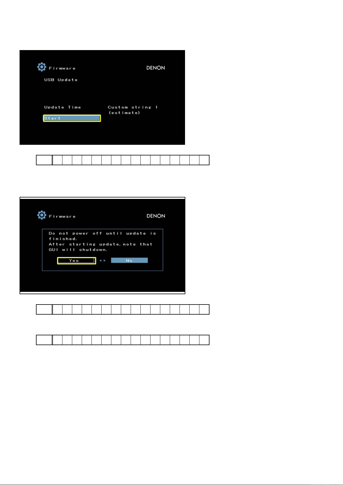
(3) Push "ENTER"
FLD
F i r m w a r e : S t a r t
(4) Select "Yes", then, Push "ENTER"
FLD
F i r m w a r e : • Y e s –
FLD
U p d a t e T i m e * * : * *
--- Precautions for Updates ---
• Never remove the USB memory before the update is nished.
• Never turn off the power before an update is completed.
• It takes around about 35 minutes to complete the update even with a broadband connection.
Once an update is started, normal operations cannot be performed until it is completed.
The GUI menu settings and image adjustment settings of this unit may be initialized.
Take note of your settings beforehand and recongure them after the update.
28
Page 29
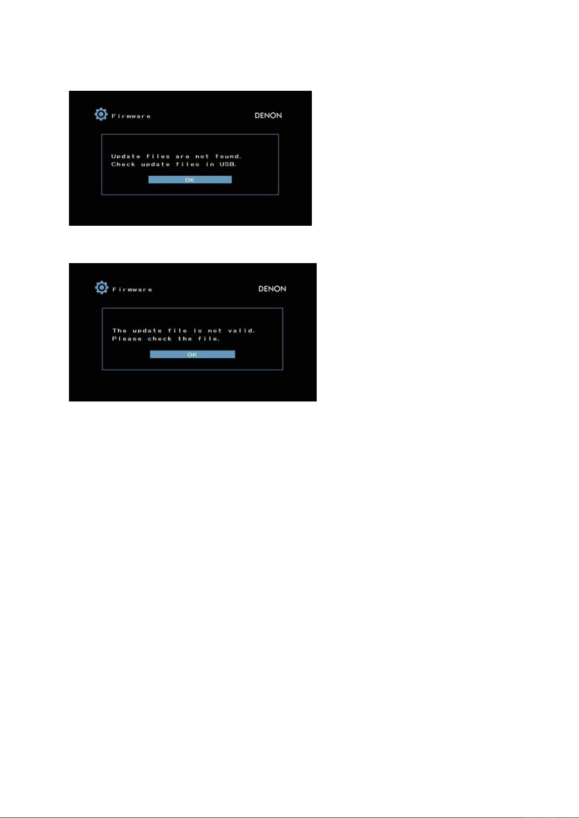
1.6. About the error code
No FirmwareFile in USB.
FirmwareFile in USB for unsupported Model name/area
29
Page 30
ADJUSTMENT
Audio Section
Adjusting Idling Current
Required measurement equipment: DC Voltmeter
1. Preparation
(1) Avoid direct blow from an air conditioner or an electric fan and humidity should be moderate, and place the set at
normal usage environment.
Temperature should be at 15 °C ~ 30 °C (59 °F ~ 86 °F).
(2) Presetting
• POWER (Power source switch) OFF
• SPEAKER (Speaker terminal) No load
(Do not connect speaker, dummy resistor, etc.)
2. Adjustment
(1) Remove the top cover and set VR510(FL), VR550(FR), VR530(C), VR520(SL), VR540(SR), on MAIN PCB at fully
counterclockwise (c) position.
(2) Connect DC Voltmeter to test points (FRONT-Lch: CN510, FRONT-Rch: CN550, CENTER ch: CN530, SURROUND-
Lch: CN520, SURROUND-Rch: CN540).
(3) Connect the power cord to AC Line, and set the power switch to "ON".
(4) Presetting.
MASTER VOLUME : c minimum
SPEAKER (Speaker terminal) : No load
(Do not connect speaker, dummy resistor, etc.)
MODE : MCH STEREO
FUNCTION : CBL/SAT
(5) Within 2 minutes after the power on, turn VR510 clockwise (x) to adjust the TEST POINT voltage at
1.5mV ± 0.5mV DC.
(6) After 10 minutes from the preset above, turn VR510 to set the voltage to 2.0mV ± 0.5mV DC.
(7) Adjust the Variable Resistors of each channel(VR520-VR550) in the same way.
DC Voltmeter
F Lch
S Lch
C ch
S Rch
F Rch
CN540VR540VR510 CN510 VR520 CN520 VR530 CN530 VR550 CN550
MAIN PCB
30
Page 31

SURROUND MODES AND PARAMETERS
Sound modes and channel output
Contents Connections Playback Settings Tips Appendix
Sound modes and surround parameters
Contents Connections Playback Settings Tips Appendix
SThis indicates the audio output channels or surround parameters that can be set.
D This indicates the audio output channels. The output channels depend on the settings of “Speaker Config.”. (v
Sound mode
p. 55)
(v
Direct (2-channel)
Direct (Multi-channel)
Stereo
Multi Ch In
Dolby Pro Logic g S D D D
DTS Neo:6
Dolby Digital
Dolby Digital Plus
Dolby TrueHD
DTS Surround
DTS 96/24
DTS-HD
DTS Express
Multi Ch Stereo
Virtual
Front L/R Center Surround L/R Subwoofer
S
S D D D
S D
S D D D
S D D D
S D D D
S D D D
S D D D
S D D D
S D D D
S D D D
S D D D
S D D D
S D
Channel output
p. 82)
z Audio is output when “Subwoofer Mode” in the menu is set to “LFE+Main”. (v p. 85)
z
D
Surr.Parameter (v
Sound mode
p. 55)
(v
Direct (2-channel)
Direct (Multi-channel)
Stereo
Multi Ch In
Dolby Pro Logic g S S S S S S S
DTS Neo:6
Dolby Digital
Dolby Digital Plus
Dolby TrueHD
DTS Surround
DTS 96/24
DTS-HD
DTS Express
Multi Ch Stereo
Virtual
This item can be selected when Dolby Digital or DTS signal is played.
z1
This item can be selected when Dolby Digital or DTS signal or DVD-Audio is played.
z2
This item can be set when the input signal is analog, PCM 48 kHz or 44.1 kHz.
z3
Mode
p. 67)
(v
S S S S S
Dynamic
z
Comp.
p. 68)
(v
S
S S
S S S S
S S S
S S S
S S
S S S
S S S
S S
S S S
S S S S
S S S S
Low
Frequency
1
(v
S S
p. 68)
Subwoofer
z
2
p. 70)
(v
z4 This setting is available when “Subwoofer Mode” in the menu is set to “LFE+Main”. (v
p. 67)
Pro Logic g Music mode only
Panorama
(v p. 69)
Dimension
(v p. 69)
p. 85)
Center Width
(v p. 69)
Neo: 6 Music
mode only
Center Image
(v p. 68)
(v
Tone
p. 52)
Restorerz3
p. 70)
(v
31
Page 32

Types of input signals, and corresponding sound modes
F This indicates the default sound mode.
DTS-HD
High
Resolution
Audio
Contents Connections Playback Settings Tips Appendix
S This indicates the selectable sound mode.
Sound mode
p. 55)
(v
DTS Surround
DTS-HD Mstr
DTS-HD Hi Res
DTS Surround
DTS 96/24
DTS Express
DTS Neo:6 Cinema
DTS Neo:6 Music
Dolby Surround
Dolby TrueHD
Dolby Digital+
Dolby Digital
Dolby Pro Logic g Cinema S S S
Dolby Pro Logic g Music S S S
Dolby Pro Logic g Game S S S
Dolby Pro Logic
Multi Ch In
Multi Ch In
Direct
Direct
Original sound mode
Multi Ch Stereo
Virtual
Stereo
Stereo
ANALOG
S S S
S S S
S S S
S S S S S S S S S S S S
S S S S S S S
S S S S S S S
F S F S S S S S S S S S
PCM DTS-HD DTS Dolby Dolby Digital
PCM
(Multi-
channel)
PCM
DTS-HD
(2-
channel)
F
Master
Audio
F
Type and format of input signals
DTS
Express
F
channel)
F
DTS
(5.1-
F
DTS 96/24
F
Dolby
TrueHD
F
Dolby
Digital Plus
F
Dolby
Digital (5.1-
channel)
Dolby
Digital
(2-
channel)
F
32
Page 33

TROUBLE SHOOTING
1. POWER
1.1. The unit does not power on
The unit does not power on
Does the power indicator
on the front panel ash in
green when the power is
turned on?
YES
Does the power display on
the front panel change to
lighting in green after approximately 10 seconds?
NO
Does the power indicator on
NO
the front panel ash in red
when the power is turned on?
NO
Has a fuse broken?
NO
Is DC5V being supplied
from the SMPS PCB (BN601)
to the DIGITAL PCB?
YES YES
Check the circuits around
the Microprocessor on the
DIGITAL PCB and replace
any faulty parts.
YES
YES
YES
See "1.2.Fuse is blown."
Is DC5V output even when
NO NO
the connector (CN751)
supplying power from the
SMPS PCB to the HDMI PCB
is removed?
Check for breakages and short circuits
in the circuits and parts between
CN751 on the DIGITAL PCB and the
microprocessor power supply and
replace any faulty parts.
Are any parts not fully connected in the connectors that
connect the PCBs?
YES
NO
TO "6. SMPS"
(See 42 page)
To "
Protection
History Display
"
mode
(See 24 page)
Has a fuse broken?
NO
Check the voltage of pins 6
- 9 of CN712 on the DIGITAL
PCB while the power display
is ashing in green.
3.3V
Disconnect the MAIN PCB connector (BN502).
Check the "Protection History Display mode"
(See 24 page)
YES
See "1.2.Fuse is blown."
Check the microprocessor ## circuit from
0V
CN751 in the DIGITAL PCB, and replace
any faulty items.
1.2. Fuse is blown
Check for leaks and short
circuits in the parts on the
primary side. Replace any
faulty parts.
Check the rectier diode in
the rectier circuit on the
secondary side, and check
the circuit for short circuits.
Replace any faulty parts.
Connect the connectors correctly.
Broken fuse
Check for short circuits between
the regulator output terminal and
GND in the power supply stabilization circuit. Replace faulty parts
if there is a short circuit.
Replace the fuse after repair.
33
Page 34
2. Analog video
MONITOR OUT(CVBS) Output NG
Check ±5VV
+5VV : C7810
-5VV : C7811
YES
Check output
Output V : IC781-1pin
YES YES
Check cable between AMP and monitor
or Check monitor.
VIDEO test point
NO
The power supply circuitry is
defective.
Check input
NO NO
(When the SAT/CBL function)
Vin3 : IC781-7pin
Check set value of IC.
NO
SW2 : IC781-10pin : 3.3V : OK
SW5 : IC781-2pin : 3.3V : OK
YES
The IC781 and surrounding
circuitry is defective.
Output V
SW2
Check pattern from JK781 to IC781 and
check cable between AMP and player or
check player .
CPU(IC711) aw.
1.+12V
2.VGND
3.-12V
4.CVBS_SW2
5.CVBS_SW5
6.+5VD
7.OPT1_IN
8.DGND
9.OPT2_IN
C7814
VIDEO PCB (B SIDE)
CN781_3 PIN
(+12V TP)
C7815
C7812
CN781_1 PIN
(+12V TP)
C7715
C7714
C7808
C7806
C7809
R7802
+5VV
R7806
IC781
SW5
R7801
C7801
Input V
C7807
-5VV
C7802
R7803
Pb
R7804
C7803
34
Page 35

3. HDMI/DVI
3.1. No picture or sound is output
No picture or sound is output.
Check HDMI/DVI cable connection.
(1) Is the HDMI/DVI cable properly connected?
YES
(2) Are you using an HDMI/DVI selector, repeater or a device for
improving picture quality?
NO
(3) Are you using a certied HDMI cable (with the HDMI stamp)?
YES
(4) Are you using an HDMI/DVI cable less than 5 meters in length?
YES
(5) Are the picture and sound output when another HDMI/DVI cable
is used?
NO
NO
There may be the a problem with the HDMI/
DVI cable. Check connection.
YES
Disconnect everything and connect only the
HDMI/DVI cable to check
NO
Use a certied HDMI cable (with the HDMI
stamp).
Replace the HDMI/DVI cable with one that
NO
is less than 5 meters in length (2 meters
recommended) to check.
YES
The HDMI/DVI cable is defective.
Check BD/DVD player.
(6) Is the BD/DVD player's HDMI output setting correct?
YES
(7) When you use a DENON BD/DVD player's, is the uorescent
display tube's "HDMI" indicator lit? If you use a non-DENON BD/
DVD player's, proceed to
NO
(9) Is sound output from the set's speaker terminals when the TV's
power is turned off or the connection cable between the TV and
the set is disconnected?
"YES".
YES
(8)
Are the picture and sound output
when the BD/DVD player's
resolution is changed?
NO
NO
(10) Are the picture and sound
output when a different BD/
DVD player is used?
NO
NO
Check the HDMI output setting, referring to
the BD/DVD player's operating instructions.
YES
Set the BD/DVD player output resolution to
a resolution with which the TV is compatible.
YES
The BD/DVD player may not be compatible
with HDCP repeaters. Ask the BD/DVD
player's manufacturer.
YES
The BD/DVD player is defective.
35
Page 36
Check TV
(11) Is the TV HDCP-compatible?
YES
(12) Is the TV compatible with resolutions of 1080P?
YES
(13) Is the TV's input set to HDMI?
YES
(14) Are the picture and sound output when a different TV is used?
YES
Check set (AV Receiver)
Is a contact part of HDMI connector normal? (See 37 page (*1).)
YES
NO
Use an HDCP-compatible TV. PC TVs
cannot be used.
If the TV is not compatible with resolutions
NO
of 1080P, no picture will be output, even
if the BD/DVD player's resolution is set to
1080P.
NO
Check the TV's input setting, referring to the
TV's operating instructions.
NO
The TV is defective.
NO
The HDMI connector is defective.
Replace the new HDMI connector.
(15) Is the set's input set to HDMI?
YES
The set does not recognize the TV.
(16) Is test point (HPD_O) set to the "H"(3V-5V)?
With the TV connected, Check voltage of the IC on the side on
which the TV is connected.
Is communication waveform conrmed in Test point (DDC_CLK/
DDC_DATA)?
Is terminate the TMDS signal
YES
(17)
When using a DENON
BD/DVD player, is the FL
display's "HDMI" indicator lit?
If using a non-DENON BD/
DVD player, proceed to "NO".
YES
is
3.3V
conrmed in D7321
The BD/DVD player does not recognize the
connection with the set.
(18)
Is HDMI connector Test point (HPD) set to the
"H"(3V-5V)?
NO NO
With the BD/DVD player connected, Check
voltage of the HDMI connector for the input on the
side on which the BD/DVD player is connected.
Is communication waveform conrmed in Test
point (DDC_CLK/DDC_DATA)?
Is terminate the TMDS signal
each HDMI connector?
HDMI IN1 : D7207-D7214
HDMI IN2 : D7220-D7227
HDMI IN3 : D7234-D7240
HDMI IN4 : D7304-D7310
HDMI IN5 : D7314-D7320
YES
-D7332?
is
NO
Check the set's input setting, referring to the
set's operating instructions.
The pattern and circuit from the HDMI
NO
connector (JK726) to the IC731 is defective,
or HDMI output circuitry is defective (IC731
and surrounding circuitry).
Replace the IC731.
The pattern and circuit
from the HDMI connector
(JK721 - 726) to the
IC721,IC731 are defective.
3.3V
conrmed
of
Replace the IC721,IC731.
Check operation of IC721,IC731.
(Video input 480P from BD/DVD players / Connect the TV.)
Replace the IC721,IC731.
36
Page 37

(19) Check power supply.
Are 1.8V or 3.3V supplied to IC721 (each power supply pin)?
q
Are 1.1V or 3.3V supplied to IC731 (each power supply pin)?
w
YES
(20) Check xtal oscillator.
Is there 28.6363MHz oscillation of X721?
q
Is there 27MHz oscillation of X731?
w
YES
(21) Check RESET.
Is RESET waveform conrmed at IC721 (97pin)? (If reference
q
waveform, proceed to "YES".)
Is RESET waveform conrmed at IC731 (114pin)? (If reference
w
waveform, proceed to "YES".)
YES
NO
The power supply circuitry is defective.
The X721 or IC721 is defective.
q
NO
NO
The X731 or IC731 is defective.
w
Replace the new parts.
The RESET pattern or IC721/IC731 is
defective.
Replace the new parts.
(22) Check control signal(I2C).
Is waveform conrmed at Test point (SDA/SCL). (If not continued
to " L", proceed to "YES".)
YES
HDMI output circuitry is defective (IC721/IC731 and surrounding
circuitry).
Replace the IC721/IC731.
NO
(*1) Abnormal sample of HDMI connector : The internal terminal has bent.
The SDATA/SCL line pattern is defective.
37
Page 38

3.2. HDMI test point and waveforms
:B
:A
A: 1.8V 2,18,21,34,36,37,45,55,61,81,93,100,103,110,126,129 pin
6,12,25,31,73,86,114,120,133,139 pinB: 3.3V
:B
:A
A: 1.1V 1, 4, 7, 13, 18, 21, 27, 49, 52, 59, 62, 69, 83, 88, 91, 98, 101, 109, 120, 125, 137 pin
10, 24, 38, 43, 44, 46, 67, 68, 85, 106, 115, 131, 138 pinB: 3.3V
Detail A
Detail
B
Detail D
HDMI test point and waveforms
DIGITAL (COMPONENT SIDE)
Detail
C
AVR-S500BT/X510BT_MP
DIGITAL_PCB
CUP12650Z_DIGITAL_MP
CUP12650Z-A
DIPPING
IN
8MHz
MEDIA PLAYER
CBL/SAT
CBL/SAT
MONITOR
COAX IN
MEDIA PLAYER
DVD/Blu-ray
BD(4K)GAME(4K)
SW
A
A
24.576MHz
27MHz
28.636MHz
OUT
B
B
C
C
SDA
SCL
SDA
SCL
CEC
CEC_COM
H_MCLK
H_LRCK
SD3
SD2
SD0
SD1
TXD_SDA
TXD_SCL
OSD_HOLD
OSD_CLK
OSD_MO
OSD_CS
OSD_MI
CEC_OUT
7623_RST
SDA
SCL
+5V
HPD
+5V
SCL
SDA
+5V
HPD
HPD
UTIL
HPD
+5V
SCL
SDA
+5V
HPD
SCL
SDA
SCL
SDA
HPD
+5V
MUTE_+B
RLY_GND
+12V
FR
SR
CENSL
FL
H/P_RLY
FRONT_RLY
C/S_RLY
AMPSIG_DET
ASO_DET
DC_PROT
THERMALDET_B
THERMALDET_A
HDMI_SDA
HDMI_SCL
SET OPTION
X
10K
10KX10K
10K
S500E1C X510E1CX510E1S500E3
4K7
10K
R7114
R7113
1.+5VA
7.MIC_SIGNAL
6.AGND
5.USB/BT_L
2.DA_GND
CN752
4.DA_GND
3.USB_/BT_R
10.USB_DAC_MUTE
9.BX_RST
8.USB_RX
7.USB_TX
6.USB_POWER1/USB1V2
4.DGND
2.D5V
1.D5V
11.USB_EN
5.USB3V3
3.DGND
CN713
12.MIC_DET
13.+12V
14.AGND
15.-12V
BAR CODE LABEL
22.FL_DATA
21.FL_CLK
20.FL_CE
19.FL_RST
19.FL_RST
17.W/G_LED
16.RED_LED
15.KEY_1
14.KEY_2
13.KEY_3
12.VSEL_B
11.VSEL_A
10.H/P_DET
9.NC
8.AGND
7.NC
6.-12V
5.+12V
4.POWER_KEY
3.MIC_DET
23.CPU_POWER
2.ISEL_B
1.ISEL_A
26.DGND
25.MCU_3V3
27.DGND
24.MCU+5V
CN711
1.SCK
CN721
7.DGND
6.MISO
5./CS
4.VCC
3.MOSI
2.DGND
1.RESET
2.MCU+3V3
3.TX
4.RX
5.DGND
6.N.C
7.BOOT
CN714
1.MCU+3V3
CN715
9.DGND
8.NJTRST
7.JTDI
6.JTMS
5.JTCK
4.JTDO
3.RESET
2.DGND
1.+12V
2.VGND
3.-12V
4.CVBS_SW2
5.CVBS_SW5
6.+5VD
7.OPT1_IN
8.OPT2_IN
9.DGND
CN741
1.DA+5V
CN771
7.VGND
6.RLY_GND
5.-12V
4.AGND(RET_GND)
3.+12V
2.DA_GND
1.MAIN_POWER
2.D_GND
3.D_GND
4.D5.2V
5.D5.2V
CN751
1.HI-B_RLY
CN712
9.THERMALDET_B
8.THERMALDET_A
7.DC_PROT
6.ASO_DET
5.AMPSIG_DET
4.C/S_RLY
3.FRONT_RLY
2.H/P_RLY
11.RLY_GND
10.+12V
9.FR
8.AGND
7.SR
6.AGND
4.AGND
2.AGND
1.FL
12.MUTE+B
5.CEN
3.SL
13.DGND
CN772
5.SDIO
9.L-OUT
8.R-OUT
7.VCC
6.SCLK
4./CE
3./RST
2.INT
1.CH_GND
TU771
ADJ2 RPIC ICT ADJ1
Pb
R7193
C7463
R7484
C7442
C7209
D7608
C7454
C7453
C7607
C7630
C7631
IC747
IC746
RN722
RN721
C7482
C7481
JK772
T7328
T7327
JK771
JK784
L7105
C7104
C7103
C7404
C7403
L7503
L7502
L7501
C7784
C7742
C7785
C7743
C7602
C7601
C7600C7599
C7285
C7603
L7511
L7119
L7104
L7103
RN733
RN732
RN731
R7294
R7293
R7512R7511
C7126
JK725
JK724
JK723 JK722
JK721
JK726
C7721
C7720
R7776
R7775
C7338
C7337
C7598
C7597
Q7503
R7526
RN734
C7124
C7735
C7734
C7733
C7732
C7596
C7595
C7594
C7593
C7592
C7145
C7144
C7143
C7142
C7141
C7120
IC731
L7129
IC755
R7541
R7369
C7728
R7424
C7675
C7695
C7694
C7678
C7662
C7661
C7639
C7706
C7617
C7700
C7699
C7684 C7683
C7667 C7666
C7710
C7704
C7624
C7623
C7620
C7619
C7692
C7691
C7686
C7685
C7674
C7669
C7668
C7659
C7658
C7653
C7652
C7241
C7240
C7638
C7622
C7621
C7572
C7565
C7561
C7554
C7539
C7532
C7517
C7510
C7679
C7556
C7580
C7557
C7544
C7406
C7341
C7340
C7339
C7218
C7521
C7520
C7381
C7371
C7361
C7358
C7355
C7349
C7345
C7343
C7434
C7441
C7440
C7816
C7614
C7613
C7611
C7610
C7716
C7713
C7551
C7576
C7467
C7465
C7461
C7439
C7131
C7130
C7129
C7123
C7122
C7709
C7703
C7702
C7698
C7682
C7665
C7641
C7615
C7612
C7605
C7591
C7590
C7586
C7583
C7582
C7579
C7575
C7573
C7564
C7562
C7550
C7549
C7545
C7543
C7540
C7531
C7528
C7527
C7526
C7525
C7524
C7523
C7518
C7509
C7508
C7507
C7505
C7504
C7503
C7502
C7474
C7473
C7472
C7466
C7464
C7462
C7460
C7458
C7455
C7447
C7443
C7438
C7437
C7432
C7431
C7430
C7302
C7301
C7279
C7271
C7270
C7233
C7220
C7217
C7134
C7127
C7125
C7121
C7119
C7114
C7560
C7558
C7574
C7563
C7559
C7555
C7541
C7519
C7230
C7229
R7721
CN752
R7634
R7633
CN712
CN751
CN771
CN741
CN711 CN772
TU771
CN713
C7506
C7501
C7697
C7696
C7681
C7680
C7664
C7663
R7191
R7560
R7559
L7527
Q7522
Q7521
R7558
R7557
Q7518
R7554
R7553
L7525
L7524
IC711
T7117
T7601
D7218 D7219
D7214
D7213
D7212
D7211
D7210
D7209
D7208
D7207
D7206
D7205
D7240
D7239
D7238
D7237
D7236
D7235
D7234
D7233
D7232D7231
D7310
D7309
D7308
D7307
D7306
D7305
D7304
D7303
D7302D7301
D7320 D7319
D7318
D7317
D7316
D7315
D7314
D7313
D7312
D7311
D7328
D7327
D7326
D7325
D7324D7323
D7322D7321
D7331
D7330
T7326
T7324
T7323
T7322
T7321
T7312
T7311
T7310
T7309
T7308
T7307
T7306
T7305
T7304 T7303
T7302
T7301
T7226
T7219
T7218
T7109T7108
T7104
T7103
T7101
Q7510
Q7508
Q7506
Q7502
Q7509
Q7507
Q7501
Q7516 Q7514
Q7515 Q7513
IC752
R7520
R7514
R7502
R7767
R7766
R7765
R7764
R7760
R7759
R7655
R7552
R7367
R7366
R7332
R7331
R7510
R7315
R7314
R7313
R7305
R7304
R7303
R7286
R7259
R7551
R7519
R7513
R7501
R7411
R7410
R7409
R7338
R7337
R7336
R7335
R7334
R7333
R7116
R7115
R7364
R7363
R7350
R7550
R7534
R7533
R7532
R7531
R7530
R7529
R7527
R7525
R7524
R7339
R7312
R7302
R7281
R7268
R7255
R7204
R7203
R7111
R7311
R7301
R7722
R7659
R7658
R7365
R7362
R7361
R7351
R7318
R7317
R7316
R7308
R7307
R7306
R7170
R7169
RN735
X731
L7402
L7401
L7308
L7307
L7306
L7305
L7304
L7303
L7302
L7301
L7601
L7523
L7522
L7521
L7512
L7510
L7509
L7429
L7508
L7127
L7126
L7125
L7124
L7123
L7122
L7120
L7117
L7116
L7115
L7114
L7113
L7112
L7111
L7110
L7109
L7108
L7107
L7106
L7102
L7101
IC761
IC722
IC743
IC764
IC763
IC762
D7102
R7696
R7712
R7710
R7694
R7680
R7678
R7705
R7704
R7703
R7702
R7689
R7688
R7687
R7686
R7673
R7672
R7671
R7670
R7205
X711
L7204
CN714
C7451
D7602
D7601
R7606
R7605
Q7109
Q7110
Q7108
R7543
D7501
T7602
T7603
T7604
T7605
T7606T7607
T7608T7609
T7116
T7115
T7114
T7113
T7112
T7111
T7110
Q7112
Q7512
Q7511
Q7113
Q7107
Q7106
Q7105
X741
R7737
R7736
X721
R7740
R7654
R7738
R7627
C7644
C7133
R7656
R7653
R7651
R7622
R7621
R7618
R7617
R7168
R7145
R7147
R7148
R7166
R7127
C7650
C7649
C7646
C7609
C7608
C7648
R7209
R7246
CN715
CN721
R7108
T7203
T7206
T7205
T7207
T7208
T7210
T7223
T7222
T7221
T7220
T7209
T7225
T7224
T7316
T7315
T7314
T7313
T7217
T7216
T7211
T7215
T7214
T7213
T7319
T7318
T7317
T7204
T7201
T7202
R7652
R7647
R7638
R7625
R7623
R7614
R7624
R7650
R7648
R7162
R7159
R7727
R7732
R7753
R7752
R7729
R7728R7730
R7743
R7742
R7741
R7734
R7715
R7714
R7699
R7698 R7683
R7682
R7666
R7604
R7603
R7744
R7668
R7667
R7664
R7665
R7601
R7602
R7718
R7723
R7724
R7719
R7725
R7726
R7713
R7711 R7697
R7695
R7681
R7679
R7107
R7403
R7757
R7758
R7735
R7745
R7620
R7619
R7616
R7615
R7241
R7251
R7202
R7240
R7239
R7238
R7258
R7250
R7201
R7156
R7160R7157
R7479
R7185
R7161
R7158
R7179
R7178
R7139
R7165
R7164
R7163
R7430
R7811
R7547
R7544
R7423
R7422
R7402
R7419
R7418
R7417
R7416
R7475
R7471
R7175
R7173
R7174
R7176
R7177
R7472
R7545
R7649
R7415
R7414
R7408
R7407
R7546
R7413
R7476
R7478
R7477
R7640
R7639
R7773
R7772
R7763
R7762
R7222
R7212
R7211
R7210
R7235
R7234
R7233
R7232
R7285
R7272
R7260
R7217
R7215
R7213
R7245
R7244
R7243
R7242
R7216
R7214
R7257
R7269
R7283
R7256
R7270
R7273
R7282
R7236
R7237
R7129
R7152
R7540
R7474
R7473
R7254
R7267
R7280
D7227
D7226
D7225
D7224
D7223
D7222
D7221
D7220
C7645
C7643
C7642
Q7609
Q7608
Q7611
T7325
J7110
J7111
J7404
J7403
Q7614
Q7612
Q7613
Q7610
D7607
D7606
D7605
D7604
D7603
RN712
L7403
D7803
RN747
RN746
RN745
RN744
RN750
RN751
RN749
RN748
RN743
RN742
RN741
RN711
Q7606
Q7605
Q7604
J7402
T7102
C7640
C7405
ET761
ET751
C7577
IC756
C7427
C7468
C7429
C7578
C7470
C7444
C7459
C7446
C7423
C7629
C7707
C7627
C7717
C7581
J7401
D7502
IC745
IC741
L7404
IC744
IC767
IC766
C7243
C7219
T7212
IC721
A
D
C
B
38
Page 39

DDC_CLK/DDC_DATA/TMDS : Check items (16),(18)
0.9V
DDC_CLK
TMDS SIGNAL
2.48V
DVDD/XTAL/RESET/SCL : Check items (19),(20),(21)
P-ON
DDC_DATA
HDMI_SDA/SCL(I2C) : Check item (22)
HDMI_SDA
HDMI_SCL
39
Page 40

4. AUDIO
4.1. AUDIO CHECK
AUDIO OUTPUT : NG
CHECK1
INPUT SURROND MODE SOURCE
ANALOG 2CH DIRECT ANALOG
OK
CHECK2
INPUT SURROND MODE SOURCE
COAX or OPT --- Legacy(PCM or DolbyDigital or dts…)
OK
CHECK3
INPUT SURROND MODE SOURCE
ANALOG 2CH
OK
CHECK4
INPUT SURROND MODE SOURCE
HDMI --- Legacy(PCM2ch or DolbyDigital or dts…)
OK
INPUT SURROND MODE SOURCE
CHECK5
HDMI ---
OK (Digital Audio BOLCK is OK)
Check other factors.
MULTI CH STEREO
ANALOG
HD AUDIO
(PCM MULTI or DolbyTrueHD or dtsHD MA)
NG
NG
Check ANALOG AUDIO BLOCK.
NG
Check Digital AUDIO BLOCK.
NG
Check via AD.
NG
Check HDMI BLOCK.
HDMI IN
OPT
IN
Analog IN
COAX
IN
CHECK6
in4-5
in1-3
②
①
Connect Setting SOURCE
HDMI OUT→other AVR HDMI IN TV MODE
HD AUDIO
(PCM MULTI or DolbyTrueHD or dtsHD MA)
OK
Check Digital AUDIO BLOCK.
HDMI
TRANSCEIVER
⑤
DSP
DIGITAL PCB
TMDS
I2S
I2S
④
I2S
DIR + CODEC
HDMI Tx
③
INPUT
SELECTOR
+
VOLUME
Check HDMI BLOCK.
HDMI PCB
MAIN PCB
NG
HDMI OUT
USB
Decode DAC
USB PCB
40
Page 41

4.2. Power AMP (MAIN UNIT)
No sound is output.
The protector operates.
YES
Is the power transistor open or shortcircuited?
2SB1560/2SD2390
NO
Is the emitter resistance of the power
transistor open?
0.47Ω
NO
Is the base resistance of the power
transistor open?
4.7Ω
NO
Is the trimmer potentiometer between the
base of the power transistor open?
1kΩ
NO
Is other transistor trouble?
NO
Is other resistance trouble?
YES
Replace the power transistor.
YES
Replace the emitter resistance.
YES
Replace the base resistance.
YES
Replace the trimmer potentiometers.
YES
Replace the transistor.
YES
Replace the resistance.
NO
Turn on the power, check that voltage of the section is normal and that idling electric current is
owing.
41
Page 42

5. Bluetooth
5.1. A connected Bluetooth device is not recognized.
Check the Bluetooth device being used
Are there other Bluetooth devices on close by?
NO
Is the Bluetooth device supported by this unit?
YES
Checking the unit
Are CN911 of the USB PCB and BT module (BX8811) correctly connected?
YES
Can a voltage (3.3V) be conrmed between pin 1 and pin 6 of CN911
on USB PCB?
YES
The circuit around IC901 of the USB PCB and BT module (BX8811) are
faulty.
YES
Turn off other Bluetooth devices.
NO
This unit supports devices with A2DP support.
NO
Connect the connectors correctly.
NO
The circuit around Q7510 of the DIGITAL
PCB.
42
Page 43
5.2. A connected USB device is not recognized.
Check the USB device being used
Is a USB hub being used?
NO
Is the USB device supported by this unit?
YES
Checking the unit
Are BN912 and BN914 of the USB PCB correctly connected?
YES
Can a voltage (5V) be conrmed between pin 1 and pin 4 of JK91 (USB
Connector) on USB PCB?
YES
The circuit between IC901 and JK91 of the USB PCB are faulty.
YES
Do not use a USB hub.
This unit supports devices in the FAT16 and
NO
FAT32-formatted mass storage class, MTPcompatible devices and iPods (with the
exception of some models).
NO
Connect the connectors correctly.
NO
IC905 around circuit of the DIGITAL PCB is
faulty.
6. SMPS
DC 5V is not output.
Is IC601 (TOP258MG) damaged?
NO
Has a fuse (F6001) broken?
NO
Are there any short circuits caused by
the soldering of the PCB?
NO
Are any parts damaged?
YES
Replace the IC601 (TOP258MG) and
D6001 - D6004.
YES
Is there the damage in D6001 - D6004?
YES
Repair the short circuited area(s) by the
soldering of the PCB.
YES
Check the damage of each part.
YES
Replace the damaged part(s).
YES
Replace the damaged part(s).
43
Page 44

OPEN(1608)
R6021
OPEN(0.2W)
C6010
OPEN
ZD619
6.8V
BN601
WIRE/5P/2.5mm
Operation waveform for each part
After primary side rectification
(Caution: High voltage, electric shock)
C6002 0.01uF 250V
D6001 1N4007
D6002 1N4007
OPEN
JUMPER
0.01uF(1608)
C6006
J6002
C6003
0.01uF 250V
*OPTION
0.1uF
0.1uF
C6007
C6009
D6003 1N4007
D6004 1N4007
D6005 1N4007
D6006 1N4007
JUMPER
ZD621
7.5V
J6003
R6006
CX602
H
R6031
1M(2125)
R6032
1M(2125)
1M(2125)
R6033
0.047uF(1608)
C6005
R6004 330K
G
1M(1608)
Q6002
INK0010AC1
D
S
OPTION
C6004
400V/100uF
E3,JP:100UF/200V
*OPTION
E1C,E1 :100UF/400V
R6012
*OPTION
IC601
TOP258MG
6 7 8 109
SMPS
(Caution: High voltage, electric shock)
Primary drain
22V
ZD611
39V
R6008
ZD608
39V
ZD609
R6009
39V
ZD610
R6010
270K
1235
2.2M(0.2W)
2.2M(0.2W)
1M(0.2W)
D6007
1N4007
22V
ZD612
22V
ZD613
C6011
1000P/1KV
22V
ZD614
22V
ZD615
22V
ZD616
22V
ZD617
R6011
10(1608)
C6026
D6012
47pF(3216)
1N4007ST
ZD618
22V
R6015
R6013
6.8(0.2W)
15K(1608)
C6013
R6014
1K(1608)
C6012
47/25V(NXA)
D6008
1N4007
C6008
50V/10UF(NXA)
0.1uF(1608)
T6001
CLT9Z093ZE
4
1
2
3
6
5
43
39V
ZD620
C6023
2200P 250V
2 1
IC602
10
8
11
7
BK603
CMD1A629
D6013
RBQ30T65A
1
2
3
After secondary rectifications
D6011
OPEN
1
2
3
4.7uF(1608)
C6014 0.1uF(1608)
C6015
C6017 OPEN
C6018 5600uF/6.3V(NXA)
C6019 5600uF/6.3V(NXA)
C6024 0.1uF(1608)
R6026
OPEN(1608)
C6025 OPEN(1608)
R6016
R6017
3.3K(0.2W)
56(0.2W)
R6018
5.6K(0.2W)
D6010 OPEN
IC603 KIA2431AP
REF
CATHODE
ANODE
R6019
C6020
0.1uF(1608)
123
R6023
R6020
22K-F(1608)
OPEN
6.8K-F
R6022
R6025
4.7K(1608)
SMPS unit
(Unloaded)
Set
A B C
A B C
44
Page 45

Personal notes:
45
Page 46

Test point
DIGITAL (COMPONENT SIDE)
AVR-S500BT/X510BT_MP
DIGITAL_PCB
CUP12650Z_DIGITAL_MP
CUP12650Z-A
DIPPING
IN
8MHz
MEDIA PLAYER
CBL/SAT
CBL/SAT
MONITOR
COAX IN
MEDIA PLAYER
DVD/Blu-ray
BD(4K)GAME(4K)
SW
A
A
24.576MHz
27MHz
28.636MHz
OUT
B
B
C
C
SDA
SCL
SDA
SCL
CEC
CEC_COM
H_MCLK
H_LRCK
SD3
SD2
SD0
SD1
TXD_SDA
TXD_SCL
OSD_HOLD
OSD_CLK
OSD_MO
OSD_CS
OSD_MI
CEC_OUT
7623_RST
SDA
SCL
+5V
HPD
+5V
SCL
SDA
+5V
HPD
HPD
UTIL
HPD
+5V
SCL
SDA
+5V
HPD
SCL
SDA
SCL
SDA
HPD
+5V
MUTE_+B
RLY_GND
+12V
FR
SR
CENSL
FL
H/P_RLY
FRONT_RLY
C/S_RLY
AMPSIG_DET
ASO_DET
DC_PROT
THERMALDET_B
THERMALDET_A
HDMI_SDA
HDMI_SCL
SET OPTION
X
10K
10KX10K
10K
S500E1C X510E1CX510E1S500E3
4K7
10K
R7114
R7113
1.+5VA
7.MIC_SIGNAL
6.AGND
5.USB/BT_L
2.DA_GND
CN752
4.DA_GND
3.USB_/BT_R
10.USB_DAC_MUTE
9.BX_RST
8.USB_RX
7.USB_TX
6.USB_POWER1/USB1V2
4.DGND
2.D5V
1.D5V
11.USB_EN
5.USB3V3
3.DGND
CN713
12.MIC_DET
13.+12V
14.AGND
15.-12V
BAR CODE LABEL
22.FL_DATA
21.FL_CLK
20.FL_CE
19.FL_RST
19.FL_RST
17.W/G_LED
16.RED_LED
15.KEY_1
14.KEY_2
13.KEY_3
12.VSEL_B
11.VSEL_A
10.H/P_DET
9.NC
8.AGND
7.NC
6.-12V
5.+12V
4.POWER_KEY
3.MIC_DET
23.CPU_POWER
2.ISEL_B
1.ISEL_A
26.DGND
25.MCU_3V3
27.DGND
24.MCU+5V
CN711
1.SCK
CN721
7.DGND
6.MISO
5./CS
4.VCC
3.MOSI
2.DGND
1.RESET
2.MCU+3V3
3.TX
4.RX
5.DGND
6.N.C
7.BOOT
CN714
1.MCU+3V3
CN715
9.DGND
8.NJTRST
7.JTDI
6.JTMS
5.JTCK
4.JTDO
3.RESET
2.DGND
1.+12V
2.VGND
3.-12V
4.CVBS_SW2
5.CVBS_SW5
6.+5VD
7.OPT1_IN
8.OPT2_IN
9.DGND
CN741
1.DA+5V
CN771
7.VGND
6.RLY_GND
5.-12V
4.AGND(RET_GND)
3.+12V
2.DA_GND
1.MAIN_POWER
2.D_GND
3.D_GND
4.D5.2V
5.D5.2V
CN751
1.HI-B_RLY
CN712
9.THERMALDET_B
8.THERMALDET_A
7.DC_PROT
6.ASO_DET
5.AMPSIG_DET
4.C/S_RLY
3.FRONT_RLY
2.H/P_RLY
11.RLY_GND
10.+12V
9.FR
8.AGND
7.SR
6.AGND
4.AGND
2.AGND
1.FL
12.MUTE+B
5.CEN
3.SL
13.DGND
CN772
5.SDIO
9.L-OUT
8.R-OUT
7.VCC
6.SCLK
4./CE
3./RST
2.INT
1.CH_GND
TU771
ADJ2 RPIC ICT ADJ1
Pb
R7193
C7463
R7484
C7442
C7209
D7608
C7454
C7453
C7607
C7630
C7631
IC747
IC746
RN722
RN721
C7482
C7481
JK772
T7328
T7327
JK771
JK784
L7105
C7104
C7103
C7404
C7403
L7503
L7502
L7501
C7784
C7742
C7785
C7743
C7602
C7601
C7600
C7599
C7285
C7603
L7511
L7119
L7104
L7103
RN733
RN732
RN731
R7294
R7293
R7512R7511
C7126
JK725
JK724
JK723 JK722
JK721
JK726
C7721
C7720
R7776
R7775
C7338
C7337
C7598
C7597
Q7503
R7526
RN734
C7124
C7735
C7734
C7733
C7732
C7596
C7595
C7594
C7593
C7592
C7145
C7144
C7143
C7142
C7141
C7120
IC731
L7129
IC755
R7541
R7369
C7728
R7424
C7675
C7695
C7694
C7678
C7662
C7661
C7639
C7706
C7617
C7700
C7699
C7684 C7683
C7667
C7666
C7710
C7704
C7624
C7623
C7620
C7619
C7692
C7691
C7686
C7685
C7674
C7669
C7668
C7659
C7658
C7653
C7652
C7241
C7240
C7638
C7622
C7621
C7572
C7565
C7561
C7554
C7539
C7532
C7517
C7510
C7679
C7556
C7580
C7557
C7544
C7406
C7341
C7340
C7339
C7218
C7521
C7520
C7381
C7371
C7361
C7358
C7355
C7349
C7345
C7343
C7434
C7441
C7440
C7816
C7614
C7613
C7611
C7610
C7716
C7713
C7551
C7576
C7467
C7465
C7461
C7439
C7131
C7130
C7129
C7123
C7122
C7709
C7703
C7702
C7698
C7682
C7665
C7641
C7615
C7612
C7605
C7591
C7590
C7586
C7583
C7582
C7579
C7575
C7573
C7564
C7562
C7550
C7549
C7545
C7543
C7540
C7531
C7528
C7527
C7526
C7525
C7524
C7523
C7518
C7509
C7508
C7507
C7505
C7504
C7503
C7502
C7474
C7473
C7472
C7466
C7464
C7462
C7460
C7458
C7455
C7447
C7443
C7438
C7437
C7432
C7431
C7430
C7302
C7301
C7279
C7271
C7270
C7233
C7220
C7217
C7134
C7127
C7125
C7121
C7119
C7114
C7560
C7558
C7574
C7563
C7559
C7555
C7541
C7519
C7230
C7229
R7721
CN752
R7634
R7633
CN712
CN751
CN771
CN741
CN711 CN772
TU771
CN713
C7506
C7501
C7697
C7696
C7681
C7680
C7664
C7663
R7191
R7560
R7559
L7527
Q7522
Q7521
R7558
R7557
Q7518
R7554
R7553
L7525
L7524
IC711
T7117
T7601
D7218 D7219
D7214
D7213
D7212
D7211
D7210
D7209
D7208
D7207
D7206
D7205
D7240
D7239
D7238
D7237
D7236
D7235
D7234
D7233
D7232D7231
D7310
D7309
D7308
D7307
D7306
D7305
D7304
D7303
D7302D7301
D7320 D7319
D7318
D7317
D7316
D7315
D7314
D7313
D7312
D7311
D7328
D7327
D7326
D7325
D7324D7323
D7322D7321
D7331
D7330
T7326
T7324
T7323
T7322
T7321
T7312
T7311
T7310
T7309
T7308
T7307
T7306
T7305
T7304 T7303
T7302
T7301
T7226
T7219
T7218
T7109T7108
T7104
T7103
T7101
Q7510
Q7508
Q7506
Q7502
Q7509
Q7507
Q7501
Q7516 Q7514
Q7515 Q7513
IC752
R7520
R7514
R7502
R7767
R7766
R7765
R7764
R7760
R7759
R7655
R7552
R7367
R7366
R7332
R7331
R7510
R7315
R7314
R7313
R7305
R7304
R7303
R7286
R7259
R7551
R7519
R7513
R7501
R7411
R7410
R7409
R7338
R7337
R7336
R7335
R7334
R7333
R7116
R7115
R7364
R7363
R7350
R7550
R7534
R7533
R7532
R7531
R7530
R7529
R7527
R7525
R7524
R7339
R7312
R7302
R7281
R7268
R7255
R7204
R7203
R7111
R7311
R7301
R7722
R7659
R7658
R7365
R7362
R7361
R7351
R7318
R7317
R7316
R7308
R7307
R7306
R7170
R7169
RN735
X731
L7402
L7401
L7308
L7307
L7306
L7305
L7304
L7303
L7302
L7301
L7601
L7523
L7522
L7521
L7512
L7510
L7509
L7429
L7508
L7127
L7126
L7125
L7124
L7123
L7122
L7120
L7117
L7116
L7115
L7114
L7113
L7112
L7111
L7110
L7109
L7108
L7107
L7106
L7102
L7101
IC761
IC722
IC743
IC764
IC763
IC762
D7102
R7696
R7712
R7710
R7694
R7680
R7678
R7705
R7704
R7703
R7702
R7689
R7688
R7687
R7686
R7673
R7672
R7671
R7670
R7205
X711
L7204
CN714
C7451
D7602
D7601
R7606
R7605
Q7109
Q7110
Q7108
R7543
D7501
T7602
T7603
T7604
T7605
T7606T7607
T7608T7609
T7116
T7115
T7114
T7113
T7112
T7111
T7110
Q7112
Q7512
Q7511
Q7113
Q7107
Q7106
Q7105
X741
R7737
R7736
X721
R7740
R7654
R7738
R7627
C7644
C7133
R7656
R7653
R7651
R7622
R7621
R7618
R7617
R7168
R7145
R7147
R7148
R7166
R7127
C7650
C7649
C7646
C7609
C7608
C7648
R7209
R7246
CN715
CN721
R7108
T7203
T7206
T7205
T7207
T7208
T7210
T7223
T7222
T7221
T7220
T7209
T7225
T7224
T7316
T7315
T7314
T7313
T7217
T7216
T7211
T7215
T7214
T7213
T7319
T7318
T7317
T7204
T7201
T7202
R7652
R7647
R7638
R7625
R7623
R7614
R7624
R7650
R7648
R7162
R7159
R7727
R7732
R7753
R7752
R7729
R7728
R7730
R7743
R7742
R7741
R7734
R7715
R7714
R7699
R7698
R7683
R7682
R7666
R7604
R7603
R7744
R7668
R7667
R7664
R7665
R7601
R7602
R7718
R7723
R7724
R7719
R7725
R7726
R7713
R7711 R7697
R7695
R7681
R7679
R7107
R7403
R7757
R7758
R7735
R7745
R7620
R7619
R7616
R7615
R7241
R7251
R7202
R7240
R7239
R7238
R7258
R7250
R7201
R7156
R7160R7157
R7479
R7185
R7161
R7158
R7179
R7178
R7139
R7165
R7164
R7163
R7430
R7811
R7547
R7544
R7423
R7422
R7402
R7419
R7418
R7417
R7416
R7475
R7471
R7175
R7173
R7174
R7176
R7177
R7472
R7545
R7649
R7415
R7414
R7408
R7407
R7546
R7413
R7476
R7478
R7477
R7640
R7639
R7773
R7772
R7763
R7762
R7222
R7212
R7211
R7210
R7235
R7234
R7233
R7232
R7285
R7272
R7260
R7217
R7215
R7213
R7245
R7244
R7243
R7242
R7216
R7214
R7257
R7269
R7283
R7256
R7270
R7273
R7282
R7236
R7237
R7129
R7152
R7540
R7474
R7473
R7254
R7267
R7280
D7227
D7226
D7225
D7224
D7223
D7222
D7221
D7220
C7645
C7643
C7642
Q7609
Q7608
Q7611
T7325
J7110
J7111
J7404
J7403
Q7614
Q7612
Q7613
Q7610
D7607
D7606
D7605
D7604
D7603
RN712
L7403
D7803
RN747
RN746
RN745
RN744
RN750
RN751
RN749
RN748
RN743
RN742
RN741
RN711
Q7606
Q7605
Q7604
J7402
T7102
C7640
C7405
ET761
ET751
C7577
IC756
C7427
C7468
C7429
C7578
C7470
C7444
C7459
C7446
C7423
C7629
C7707
C7627
C7717
C7581
J7401
D7502
IC745
IC741
L7404
IC744
IC767
IC766
C7243
C7219
T7212
IC721
q
w
e
(47)RXP2/GPO2
(32)DAI2_LRCK
(33)DAI2_SCLK
(34)DAI2_DATA,DSD5
RMCK(55)
SAI_SCLK(61)
SAI_LRCK(60)
SAI_SDOUT(54)
IC744
CS42528
(DIR+CODEC)
IC741
CS497024CVZ
(AUDIO DSP)
(49)RXP0
(59)OMCK
(3)CX_LRCK
(2)CX_SCLK
(1)CX_SDIN1
(64)CX_SDIN2
(63)CX_SDIN3
(62)CX_SDIN4
(35) CH0 ASD1
(36) CH0 ASD0
(34) CH0 ASD2
(33) CH0 ASD3
(32) CH0 ALRCK
(31) CH0 ABCLK
(136) CH0 AMCLK
(47)DAO1_D3
(48)DAO1_D2,HS2
(49)DAO1_DATA1,HS1
(51)DAO1_DATA0,HS0
DAI1_DATA0,DSD0(27)
DAI1_DATA1,DSD1(26)
DAI1_DATA2,DSD2(24)
DAI1_DATA3,DSD3(23)
(52)DAO1_SCLK
(54)DAO1_LRCLK
(16)XTAL_OUT
DAI1_LRCK,DSD4(30)
DAI1_SCLK,DSD-CLK(29)
DAO_MCLK(40)
Coaxial1
Optical1
IC721 ADV7623BSDZ
HDMI
Transceiver
(W/GUI)
HDMI 1 - 3
HDMI 4 - 5
IC731
MN8647781
CH1: RXP2
1
CH1: DATA0
CH2: LRCK1
CH3: SCLK1
CH4: X-OUT
3
CH1: SDOUT
CH2: LRCLK2
CH3: SCLK2
2
Wave form
DIPPING
MEDIA PLAYER
CBL/SAT
CBL/SAT
COAX IN
SW
24.576MHz
OUT
SCL
SCL
SDA
HPD
+5V
1.+5VA
7.MIC_SIGNAL
6.AGND
5.USB/BT_L
2.DA_GND
CN752
4.DA_GND
3.USB_/BT_R
10.USB_DAC_MUTE
9.BX_RST
8.USB_RX
7.USB_TX
6.USB_POWER1/USB1V2
4.DGND
2.D5V
1.D5V
11.USB_EN
5.USB3V3
3.DGND
CN713
12.MIC_DET
13.+12V
14.AGND
15.-12V
5.SDIO
9.L-OUT
8.R-OUT
7.VCC
6.SCLK
4./CE
3./RST
2.INT
1.CH_GND
TU771
R7193
C7463
R7484
C7454
C7453
C7607
C7630
C7631
JK772
JK771
JK784
C7404
C7403
JK721
C7721
C7720
R7776
R7775
C7124
C7735
C7734
C7142
C7728
C7675
C7695
C7694
C7678
C7662
C7661
C7639
C7706
C7617
C7700
C7699
C7684 C7683
C7667 C7666
C7710
C7704
C7624
C7623
C7620
C7619
C7692
C7691
C7686
C7685
C7674
C7669
C7668
C7659
C7658
C7653
C7652
C7638
C7622
C7621
C7679
C7521
C7816
C7614
C7613
C7611
C7610
C7467
C7465
C7461
C7709
C7703
C7702
C7698
C7682
C7665
C7615
C7612
C7605
C7590
C7474
C7473
C7466
C7464
C7462
C7460
C7458
C7455
C7447
C7270
C7121
CN752
R7634
R7633
TU771
C7697
C7696
C7681
C7680
C7664
C7663
Q7522
R7558
R7557
D7214
D7213
D7212
D7211
D7210
D7209
D7208
D7207
D7206
D7205
R7765
R7764
R7655
R7259
R7411
R7410
R7409
R7255
R7659
R7658
L7601
IC761
IC764
IC763
IC762
R7696
R7712
R7710
R7694
R7680
R7678
R7705
R7704
R7703
R7702
R7689
R7688
R7687
R7686
R7673
R7672
R7671
R7670
C7451
R7606
R7605
X741
R7740
R7654
R7738
R7627
C7644
R7656
R7653
R7651
R7622
R7621
R7618
R7617
C7650
C7649
C7646
C7609
C7608
C7648
T7203
T7205
T7204
T7201
T7202
R7638
R7625
R7623
R7614
R7624
R7727
R7732
R7753
R7752
R7729
R7728R7730
R7743
R7742
R7741
R7715
R7714
R7699
R7698 R7683
R7682
R7666
R7604
R7603
R7744
R7668
R7667
R7664
R7665
R7601
R7602
R7718
R7723
R7724
R7719
R7725
R7726
R7713
R7711 R7697
R7695
R7681
R7679
R7403
R7757
R7758
R7745
R7620
R7619
R7616
R7615
R7258
R7479
R7811
R7417
R7416
R7475
R7471
R7472
R7415
R7414
R7408
R7407
R7413
R7476
R7478
R7477
R7640
R7639
R7260
R7257
R7269
R7256
R7474
R7473
R7254
C7645
C7643
C7642
Q7609
Q7608
Q7611
J7404
J7403
Q7610
D7604
D7603
L7403
D7803
RN750
RN751
RN749
RN748
RN743
Q7606
Q7605
Q7604
J7402
C7468
C7470
C7444
C7459
C7446
C7423
C7629
C7707
C7627
J7401
L7404
IC744
IC767
IC766
X-out
LRCK1
SCLK1
DATA0
SDOUT
LRCK2
RXP2
SCLK2
Detail A
CLOCK FLOW & WAVE FORM IN DIGITAL BLOCK
A
46
Page 47

ANALOG AUDIO BLOCK DIAGRAM
AVR-S500BT/X510BT ANALOG AUDIO BLOCK
AUDIO IN
DVD
SAT/CBL
SETUP MIC
MIC
TUNER
TUNER
FM/AM
MAIN
ANA_FL
DA_FL
ANA_FR
DA_FR
DA_CEN
DA_SW
DA_SL
DA_SR
DA_SBL
MAIN AMP
2SD2390/2SB1560
H/P OUT
SPK OUT
+
-
+
-
+
-
+
-
+
-
H/P L
GND
H/P R
FL
FR
CEN
SL
SR
TO DIGITAL
AUDIO BLOCK
AD_FL
AD_FR
USB/BT_IN
DA_FL
DA_FR
DA_CEN
DA_SW
DA_SL
DA_SR
DA_SBR
VOL IC
NJU72340A
PRE OUT
SW1MUTE
SW2
47
Page 48

DIGITAL AUDIO/HDMI BLOCK DIAGRAM
AVR-S500BT/X510BT DIGITAL AUDIO/HDMI BLOCK
DIGTAL IN
DIR IN OPTION
S500BT
X510BT
OPTICAL IN1
OPTICAL IN2
COAXIAL IN1
COAX IN
1
0
BT
MODULE
UART
LRCK
SCLK
SD0
SD1
SD2
SD3
+
-
+
-
CODEC
SERIAL
PORT
ADC
ADC
INPUT
SELECT
DIR/CODEC
CS42528
VOLUME
CONTROL
DIGITAL
FILTER
DIGITAL
FILTER
Rx
GAIN
&
CLIP
GAIN
&
CLIP
CLK/DATA
RECOVERY
DIGITAL
FILTER
ADC
SERIAL
DATA
OMCK
RMCK
DAC
DAC
DAC
DAC
DAC
DAC
DAC
DAC
DEM
S/PDIF
DECODER
ANALOG
FILTER
SERIAL
AUDIO I/F
DA_FL
DA_FR
DA_CEN
DA_SW
DA_SL
DA_SR
SAI_LRCK
SAI_SCLK
SAI_SDO
USB IN
HDMI IN1
HDMI IN2
HDMI IN3
HDMI IN4
HDMI IN5
D+/-
USB
TMDS
TMDS
TMDS
TMDS
TMDS
DECORDER
(BX8804)
USB
AUDIO DACI2S
(PCM5100)
S.FLASH
32M
For GUI
HDMI RX
ADV7623
2S SDATA0,1,2,3, SCLK, LRCLK, MCLK
I
TMDS
HDMI TX(4K)
MN8647781
SPDIF
I2S SDATA0,1,2,3, SCLK, LRCLK, MCLK
I2S SDATA0,1,2,3, SCLK, LRCLK, MCLK
TC74VHC157FT
HDMI MCLK
MCLK
MUX
TC74VHC157FT * 2
MUX
LRCK
SCLK
SD0
SD1
SD2
SD3
I2S SDATA0,1,2,3, SCLK, LRCLK
DAO_MCK
XOUT
S.FLASH
8M
DSP
CS497024
SDRAM
16M
--
--
AD_FL
AD_FR
DA_FL
DA_FR
DA_CEN
DA_SW
DA_SL
DA_SR
USB/BT_IN
HDMI OUT
TO ANALOG
AUDIO BLOCK
48
Page 49
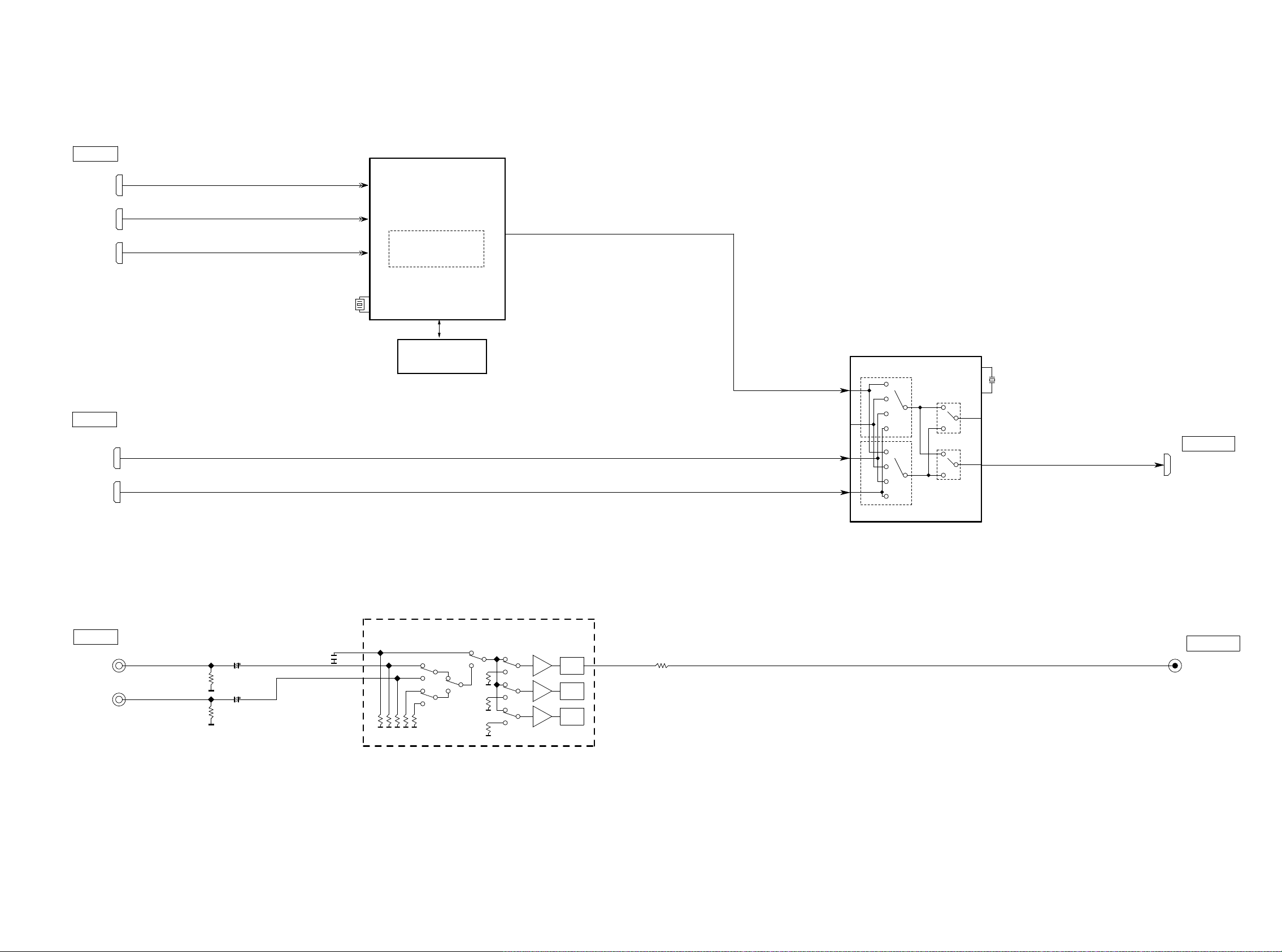
VIDEO BLOCK DIAGRAM
AVR-S500BT/X510BT VIDEO BLOCK
HDMI IN
HDMI IN1
(CBL/SAT)
HDMI IN2
(BLU-RAY)
HDMI IN3
(AUX)
HDMI IN
HDMI IN4
(GAME)
HDMI IN5
(MEDIA Player)
RXC
RXD
P1 RX
P0 RX
RXB
X7201
28.6363MHz
ADV7623
TRANSCEIVER
OSD Block
S.FLASH
32M
For GUI
P3 RX
P1 RX
P0 RX
HDMI TX(MN864778)
MAIN
SUB
27.000MHz
P0 TX
P1 TX
HDMI OUT
MONITOR OUT
CVBS IN
Media Player
SAT/CBL
NJM2595
20K
20K
20K
20K
6dB
6dB
6dB
75ohm
Driver
75ohm
Driver
75ohm
Driver
CVBS OUT
MONITOR OUT
49
Page 50

POWER BLOCK DIAGRAM
AVR-S500BT/X510BT VCC DIAGRAM
!
AC CORD
RELAY
!
!
S1(AMP+B,-B)
S2(+12V,-12V)
MAIN TRANS
S4(FL+Vdisp)
HI+B
LOW+B
HI-B
LOW-B
MAIN+B
2
4
1
3
MM1Z7V5
NJM2845DL133
KIA7805BPI
185.1mA
14mA
50mA
37.5mA
KIA7812BPI
MM1Z7V5
22mA
MM1Z5V1
KIA7912PI
MM1Z5V1
MAIN-B
RELAY*5
VOLUME IC
25mA
(NJU72340A)
A+12V
32mA
(NJM8080 X 4)
45mA
DA+3.3V (USB DAC:PCM5100)
+5VA
TUNER+5V
CS42528(VA)
A-12V
VOLUME IC
(NJU72340A)
V+5V
(NJM
V-5V
(NJM2595)
68mA
Vdisp(+37V)
(NJM2115MDTE1 X 2)
S2 TOTAL : 410.6mA
2595)
!
163mA
FILAMENT AC
S5(FILAMENT)
FILAMENT AC
INPUT CURRENT (Ref Volage:5.2V)
*DC-DC Effieciency:85%
SMPS Total Current : About 3237.77 mA
20mA
122.5mA
1000mA
+5.2V
1036.3mA
(5.2V)
EN5339QI(+3.3V)
357.5mA
343mA
OPEN
339mA
445mA
D
G
43
2 1
60mA
(5.2V)
S
542.18mA
MAIN PWR ON
(5.2V)
* RESERVED
EN5339QI(+1.2V)
OPEN
EN5339QI(+1.8V)
(5.2V)
60mA
BU12TD3WG
982mA
380mA
296.79mA
(5.2V)
160mA
(5.2V)
EN5339QI(+1.1V)
NJM2845DL133
1220mA
160mA
FRONT LED(CVDBLBJEGJ204L)
MCU+5V
CS42528(VD), OPTICAL JACK X 2
D5V/VBUS
CEC5V/HDMI & DSP
+3V3D/DIR,DSP
(CS497024,CS42528,M12L16161A5TG2Q,MX25L8006EM2I-12G,TC74VHC157FT X 3)
CEC3V3/HDMI
(MN864778)
DV3.3V/ADV7623,MX25L3206E)
USB3.3V/BX8804,W9864G6JH-6,MX25L1606EM2I-12G)
USB1V2/USB
(BX8804)
USB1V2/USB
(BX8804)
D1V8H/HDMI
(ADV7623)
+1V8/DSP
(CS497024)
CEC1V1/HDMI TX
(MN864778)
MCU_3V3/MICOM
(STM32F101ZG,M24C32WMN6TP,PST8425NR,VFD)
* TOTAL (5V): 1142.5mA
50
SWM3V3/DETECT PULLUP
Page 51

LEVEL DIAGRAM
AVR-S500BT/X510BT LEVEL1 DIAGRAM
FRONT ch
AUDIO IN
DIGITAL
40dB
2CH IN 0dB
(200mV)
-10dB
-20dB
30dB
20dB
10dB
FRONT
-2.78dB
A/D IN
REV AMP
A/D IN
REV AMP
CS42528
DIFF. INPUT
0dBFS=5.6Vpp
AD IN=145mV
A/D
=1.98Vrms
A/D
DIR
0dBFS
-10dBFS
-20dBFS
-22.78dBFS
(A/D IN)
-30dBFS
-40dBFS
DSP
CS42528
0dBFS
-10dBFS
-20dBFS(DIG.IN)
-22.78dBFS
(A/D IN)
-30dBFS
-32dBFS(DIG.IN)
-34.78dBFS
(A/D IN)
-40dBFS
D/A
D/A
CS42528
DIFF. OUT
0dBFS=5Vpp
=1.77Vrms
D/A OUT
LPF
FULL SCALE LEVEL=2Vrms
DOLBY LIMIT LEVEL (ALL ch-3dBFS)
+1.77dB
+1.77dB
+1.77dB
+1.77dB
ELECTRIC
VOLUME
NJU72340AFH3
VOL 00
PRE AMP1
-2dB
+1dB
+10dB
+13dB
GAIN setting of MASTER VOL 00dB
-SW:YES(DIGITAL)
-SW:YES(ANALOG)
-SW:NONE(DIGITAL)
-SW:NONE(ANALOG)
=-2dB
=+1dB
=+10dB
=+13dB
+29dB
POWER AMP
-24dB
ATT
40dB
30dB
20dB
10dB
-10dB
-20dB
0dB
SPK OUT
FRONT
H/P OUT
SPK OUT
FRONT
4.47Vrms/8ohm
H/P OUT
282mVrms
/33ohm
51
Page 52

AVR-S500BT/X510BT LEVEL2 DIAGRAM
CENTER ch
40dB
2CH IN 0dB
(200mV)
-10dB
-20dB
30dB
20dB
10dB
CENTER
DSP OUT D/A
D/A
CS42528
DIFF. OUT
0dBFS=5Vpp
=1.77Vrms
0dBFS
-10dBFS
-20dBFS(DIG.IN)
-22.78dBFS
(A/D IN)
-30dBFS
-40dBFS
D/A OUT
LPF
FULL SCALE LEVEL=2Vrms
DOLBY LIMIT LEVEL (ALL ch-3dBFS)
+1.77dB
+1.77dB
ELECTRIC
VOLUME
NJU72340AFH3
VOL 00
PRE AMP1
-2dB
+1dB
GAIN setting of MASTER VOL 00dB
-PCM or DD Config1(DIG.IN) =-2dB
-A/D IN(ANALOG)
-DD Config2(DIG.IN)
=+1dB
=+1dB
+29dB
POWER AMP
40dB
30dB
20d
10dB
-10dB
-20dB
0dB
SPK OUT
CENTER
SPK OUT
FRONT
B
4.47Vrms/8ohm
52
Page 53

AVR-S500BT/X510BT LEVEL3 DIAGRAM
SURROUND ch
40dB
2CH IN 0dB
(200mV)
-10dB
-20dB
30dB
20dB
10dB
SURROUND
DSP OUT D/A
D/A
CS42528
DIFF. OUT
0dBFS=5Vpp
=1.77Vrms
0dBFS
-10dBFS
-20dBFS(DIG.IN)
-22.78dBFS
(A/D IN)
-30dBFS
-40dBFS
D/A OUT
LPF
FULL SCALE LEVEL=2Vrms
DOLBY LIMIT LEVEL (ALL ch-3dBFS)
+1.77dB
+1.77dB
ELECTRIC
VOLUME
NJU72340AFH3
VOL 00
PRE AMP1
-2dB
+1dB
GAIN setting of MASTER VOL 00dB
-PCM or DD Config1(DIG.IN) =-2dB
-A/D IN(ANALOG)
-DD Config2(DIG.IN)
=+1dB
=+1dB
+29dB
POWER AMP
40d
30dB
20dB
10dB
-10dB
-20dB
0dB
SPK OUT
SURROUND
B
SPK OUT
FRONT
4.47Vrms/8ohm
53
Page 54

AVR-S500BT/X510BT LEVEL4 DIAGRAM
SUBWOOFER ch
40dB
30dB
20dB
SUBWOOFER
DSP OUT
0dBFS
D/A
D/A
CS42528
DIFF. OUT
0dBFS=5Vpp
=1.77Vrms
D/A OUT
LPF
REV AMP
FULL SCALE LEVEL=2Vrms
DOLBY LIMIT LEVEL (ALL ch-3dBFS)
SW SUM
REV AMP
ELECTRIC
VOLUME
NJU72340AFH3
PRE AMP1
MUTE
40dB
30dB
20dB
SW WOOFER
PREOUT
2CH IN 0dB
(200mV)
-10dB
-20dB
10dB
-10dBFS
-20dBFS
-30dBFS(DIG.IN)
DD Config1
-37dBFS(A/D IN)
-40dBFS
+8.2dB
+8.2dB
VOL 00
+12dB
+15dB
10dB
-10dB
-20dB
0dB
PREOUT
SUBWOOFER
500mVrms
PREOUT
SUBWOOFER
316mVrms
54
Page 55

WIRING DIAGRAM
AVR-S500BT/X510BT WIRING DIAGRAM
CN602
2P
SMPS<-AC IN
AC CORD
SMPS<-DIGITAL
TUNER
CN781
DIGITAL PCB
CN771
7P
CN751
5P
CN741
9P
CN711
27P
9P
CN772
13P
VIDEO PCB
CN712
9P
CN713
15P
CN752
7P
BN508
9P/9P
TU771
TRANS
TRANS -> FRONT
5P
SMPS PCB
CN102
7P
BN101-1
9P
STANDBY<->FRONT
9P
BN101
STANDBY
PCB
CN601
2P
TRANS -> SMPS
BN601
REGULATOR PCB
CN302
5P
TRANS -> REGUL.
TRANS->MAIN
PHONE <- MAIN
CN103
3P
3P
CN104
3P
BN131
PHONE PCB
7P
PHONE-FRONT
BN301
REGUL.<- DIGITAL
BN505
3P
FRONT PCB
BT MODULE
CN503
10P
7P
13P
BN501
MAIN->DIGITAL
BN502
MAIN->DIGITAL
9P
MAIN PCB
FRONT <-> DIGITAL
27P
BN12B1
USB & MIC <-> DIGITAL
USB & MIC <-> DIGITAL
CN911
10P
USB
USB & MIC PCB
7P
BN914
MIC
15P
BN912
55
Page 56
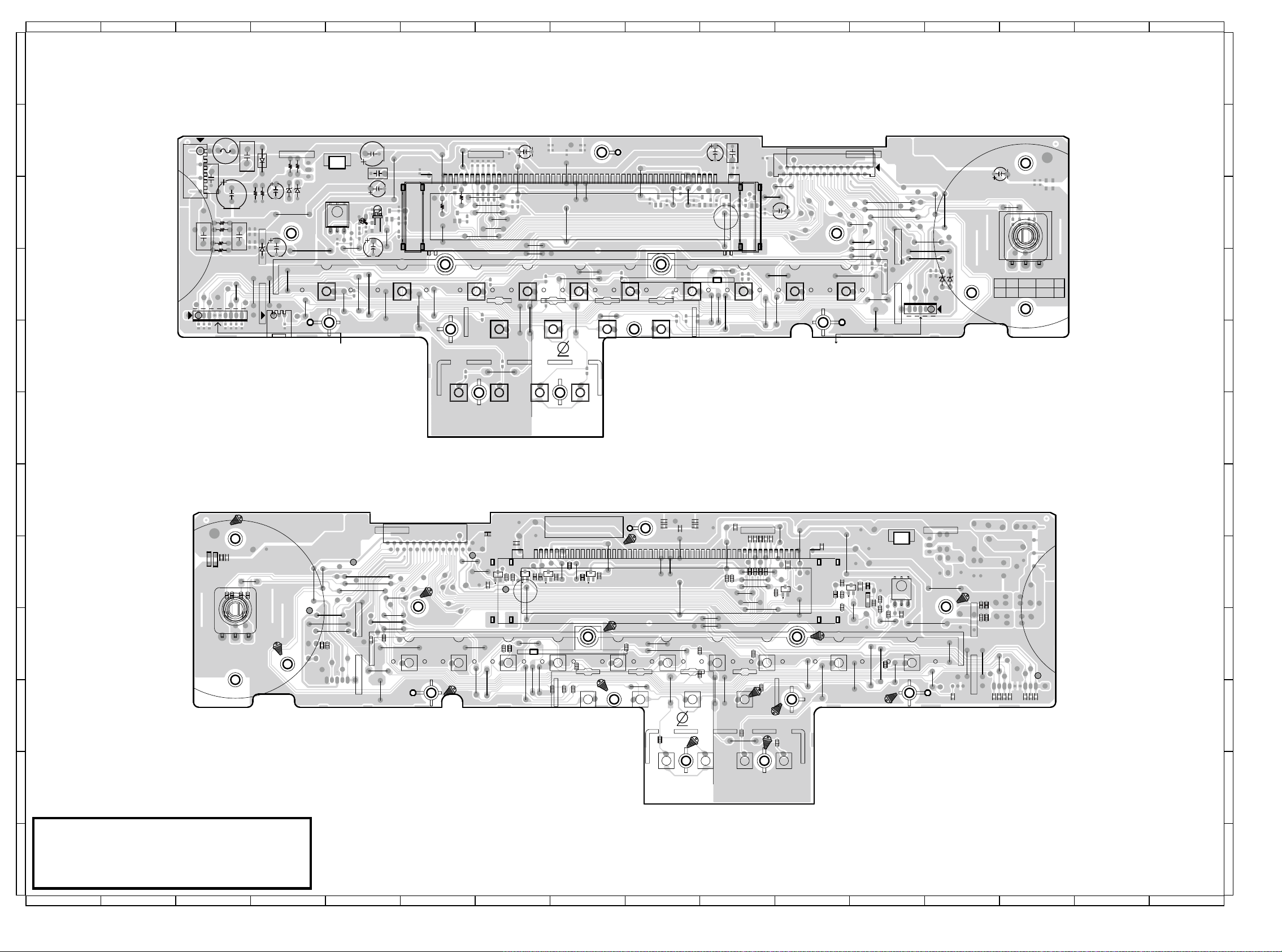
1 2 3 4 5 6 7 8 9 10 11 12 13 14 15 16
PRINTED WIRING BOARDS
A
A
FRONT
(A SIDE)
C1001
2.ISEL_A
3.ISEL_B
4.DGND
C1079
R1001
R1002
R1004
R1003
6.GRN_LED
7.RED_LED
5.DGND
T 100mA L 250V
OPEN
OPEN
F1001
OPEN
OPEN
C1005
8.MCU+5
9.POWER_KEY
C1080
J1065
C1002
R1417
D1003
J1009
R1029
J1012
CN103
D1001
C1006
J1005
C1003
J1034
1.D GND
2.D GND
R1007
S500BT/X51OBT : SOUND-
J1014
3.H/P DET
R1062D1005
Q1001
D1004
RC101
J1006
S700W : ZONE2 ON/OFF
X1100W : PRESET-
J1072
SW106
C1004
J1067
C1007
C1008
LD101
J1069
C1038
S500BT/X51OBT : SOUND+
S700W : ZONE2 SEL
X1100W : PRESET+
J1071
J1070
J1018
J1039
J1040
S700W : PRESET+
X1100W : ZONE2 SEL
SW109
J1058
J1059
S500BT/S700W : Q/S_2
MP STAGE
S500BT : TONE
S700W : GAME
C1010
J1056
SW113
J1025
J1026
J1027
J1049
J1054
S500BT/S700W : TUNE-
S700W : PRESET+
X510BT/X1100W : DIMMER
SW116
S500BT/S700W : Q/S_3 S500BT/S700W : Q/S_4
J1074
J1057
SW119
Pb
Pb
S500BT : NIGHT
S700W : PURE
S500BT/S700W : TUNE+
X510BT/X1100W : STATUS
SW104
J1028
J1029
X510BT/X1100W : Q/S_1
SW112
J1017
J1007
572 572
572 572
J1015
J1019
J1020
J1021
J1008
SW115
BK101
BK101
J1052
J1064
J1068
S500BT/S700W : RESTORE
R1030
S500BT/X51OBT : PRESET- S500BT/X51OBT : PRESET+
X1100W : ZONE2 ON/OFF
R1067
J1024
S700W : PRESET-
SW105
S500BT/S700W : Q/S_1
J1051
J1061
S500BT : EQ
S700W : MUSIC
J1022
SW107
CUP12619Z-1
FRONT PART
C1018
J1030
S500BT/S700W : BAND
SW117
J1048
J1031
J1041
S500BT/S700W : MODE
X510BT/X1100W : Q/S_2
J1046
J1045
C1017
FL101
BK102
BK102
SW110
BN12B1
J1033
J1035
J1038
J1036
C1019
S500BT/S700W : BAND
X510BT/X1100W : Q/S_1
SW118
S500BT/S700W : DIMMER
X510BT/X1100W : Q/S_3
J1037
J1003
J1047
J1023
SW 111
S500BT/S700W : STATUS
X510BT/X1100W : Q/S_4
J1004
J1066
J1053
J1032
25.MCU_3V3
26.D_GND
27.D_GND
25.MCU_3V3
26.D_GND
27.D_GND
J1042
J1043
J1044
19.FL_RST
20.FL_CE
21.FL_CLK
22.FL_DATA
23.CPU_POWER
24.MCU_5V
19.FL_RST
20.FL_CE
21.FL_CLK
22.FL_DATA
23.CPU_POWER
24.MCU_5V
BN12A
15.KEY_1
16.RED_LED
17.GRN_LED
18.RC_IN
15.KEY_1
16.RED_LED
17.GRN_LED
18.RC_IN
J1002
J1010
J1016
J1011
D1403
12.VSEL_B
13.KEY_3
14.KEY_2
12.VSEL_B
13.KEY_3
14.KEY_2
D1402
7.MIC_SIGNAL
8.A_GND
9.B/P_IRIN_DE
10.H/P_DET
11.VSEL_A
7.MIC_SIGNAL
8.A_GND
9.B/P_IRIN_DE
10.H/P_DET
11.VSEL_A
J1001
5. MIC DET
3. -12V
4. +12V
2. MIC SIGNAL
4.POWER_KEY
5. +12V
6. -12V
4.POWER_KEY
5. +12V
6. -12V
1. A GND
2.ISEL_B
1.ISEL_A
3.MIC_DET
2.ISEL_B
1.ISEL_A
3.MIC_DET
VR101
C1075
J1050
IC RPADJ2ADJ1ICT
LUG11
B
C
C
C
B
B
A
A
D
E
B
CN102
C
1.VDISP
2.NC
3.GND
4.NC
5.FL AC
6.NC
7.FL AC
D
1.+3v3
BN101_1
E
SW108
F
SW114
SW103
SW102
F
FRONT
(B SIDE)
G
C1422
1.ISEL_A
2.ISEL_B
3.MIC_DET
5. +12V
6. -12V
7.MIC_SIGNAL
4.POWER_KEY
8.A_GND
9.B/P_IRIN_DE
13.KEY_3
10.H/P_DET
11.VSEL_A
12.VSEL_B
13.KEY_3
14.KEY_2
15.KEY_1
16.RED_LED
14.KEY_2
15.KEY_1
16.RED_LED
17.GRN_LED
18.RC_IN
19.FL_RST
20.FL_CE
21.FL_CLK
17.GRN_LED
18.RC_IN
19.FL_RST
20.FL_CE
21.FL_CLK
22.FL_DATA
23.CPU_POWER
24.MCU_5V
25.MCU_3V3
26.D_GND
22.FL_DATA
23.CPU_POWER
24.MCU_5V
25.MCU_3V3
26.D_GND
27.D_GND
27.D_GND
L1001
BAR CODE
LABEL
C1419
C1421
C1418
C1420
C1012
C1013
C1014
C1015
C1016
C1011
C1423
C1041
+3V3
S500BT/S700W : MODE
X510BT/X1100W : Q/S_2
Q1006
C1020
R1079
+5V
R1021
R1020
R1078
Q1005
R1019
R1017
S500BT/S700W : BAND
X510BT/X1100W : Q/S_1
Q1004
R1084
R1026
R1085
R1018
R1080
Q1003
R1025
R1016
S500BT/S700W : TUNE+
X510BT/X1100W : STATUS
R1083
R1072
S500BT/S700W : Q/S_3S500BT/S700W : Q/S_4
S500BT/S700W : TUNE-
X510BT/X1100W : DIMMER
S500BT/S700W : Q/S_2
Pb
R1071
S500BT : NIGHT
S700W : PURE
S500BT/X51OBT : PRESET+
S700W : PRESET+
R1077
R1082
S500BT : TONE
S700W : GAME
C1409
R1410
2.MIC SIGNAL
1.A GND
3.-12V
+12V
5.MIC DET
4.+12V
C1082
R1046
S500BT/S700W : STATUS
X510BT/X1100W : Q/S_4
GND
GND
S500BT/S700W : DIMMER
X510BT/X1100W : Q/S_3
C1073
C1074
D1015
H
J
D1016
R1061
R1058
C1076
C B A
C B A
C1077
R1059
R1060
GND
GND
-12V
K
R1012
R1013
R1014
R1015
R1010
R1011
S500BT/X51OBT : PRESET-
S500BT/S700W : Q/S_1
R1081
S500BT : EQ
S700W : MUSIC
S700W : PRESET-
X1100W : ZONE2 ON/OFFX1100W : ZONE2 SEL
R1073
R1068
Q1002
R1075
S500BT/S700W : RESTORE
C1009
R1076
R1023
GND
GND
R1022
R1053
S500BT/X51OBT : SOUND+
S700W : ZONE2 SEL
X1100W : PRESET+
R1069
Q1007
C1430
D1408
R1420
GND
GND
R1421
CUP12619Z-1/FRONT PART/MP STAGE
R1419
R1418
C1039
R1024
S500BT/X51OBT : SOUND-
S700W : ZONE2 ON/OFF
X1100W : PRESET-
R1074
3.H/P DET
2.D GND
1.D GND
C1081
R1009
R1008
R1005
C1090
C1091
R1006
C1089
C1088
4.DGND
5.DGND
6.GRN_LED
7.RED_LED
8.MCU+5
9.POWER_KEY
1.VDISP
2.NC
3.GND
4.NC
5.FL AC
6.NC
7.FL AC
2.ISEL_A
3.ISEL_B
1.+3v3
+3V3
C1087
C1086
C1085
G
H
J
K
L
鉛フリー半田
半田付けには、鉛フリー半田 (Sn-Ag-Cu) を使用してください。
M
Lead-free Solder
When soldering, use the Lead-free Solder (Sn-Ag-Cu).
1 2 3 4 5 6 7 8 9 10 11 12 13 14 15 16
L
M
56
Page 57

1 2 3 4 5 6 7 8 9 10 11 12 13 14 15 16
PRINTED WIRING BOARDS
A
MAIN
(A SIDE)
B
C
D
E
F
G
D5701
J5901
J5902
F5802
J5934
J5805
J5933
CN503
1.HP_RCH
BN505
RY586
2.AGND
3.HP_LCH
D5701
J5905
T5A L 250V
J5906
7.AC_L
SL
SR
CEN
FL
FR
A
CMD1A569
J5601
J5628
BK501
J5629
J5630
J5631
J5632
J5633
J5634
J5636
J5635
C5715
J5642
D5806
J5804
6.NC
5.AC_H
4.CEN
3.AC_H
2.NC
1.AC_L
R5726
R5727
C5706
R5710
R5709
J5637
C5703
J5638
J5639
C5714
C5702
J5640
J5641
C5704
J5903
J5904
F5801
T5A L 250V
D5601
RY560
R5107
D5101
R5108
R5109
R5103
C5106
C5104
J5108
R5129
R5106
J5118
J5111
R5130
R5104
R5102
Q5101
Q5102
C5102
C5103
R5110
C5105 C5205
J5112
R5132
R5121
R5119
L5101
R5131
R5124
R5127
R5128
C5109
C5108
R5125
D5106
R5123
J5107
D5105
D5103
R5111
D5102
D5104
R5112
C5107
R5116
J5106
CN510 R5114
R5115
J5102
J5104
VR510
R5113
R5117
R5118
J5103
2SD2390
E C B E BC E BC E BC E C E BC E BC B E BC E BC
B E E EB B
E
J5607
R5101
C5101
J5606
D5201
R5105
Q5103 Q5203 Q5303 Q5403 Q5503
J5113
Q5106Q5105 Q5104
2SB1560 2SB1560
J5605 J5608
J5101
J5604
J5602
J5114
J5115
J5116
J5109
R5122
R5120
D5206
R5224
C5209
C5208
R5223
D5202
D5204
J5206
C5207
R5216
D5203
R5212
R5215
R5213
R5217
J5105
C5615
R5704
R5703
J5645
J5644
J5646
J5649
J5650
J5616
J5610
J5611
J5609
C5204
R5208
J5208
R5209
J5210
R5207
C5206
R5229
R5206
R5221
R5219
R5230
R5203
Q5201
Q5202
J5218
C5203
J5211
J5212
L5201
R5231
R5227
R5228
R5225
R5211
J5207
R5214
D5205
VR520
J5203
J5202
J5204
2SD2390 2SD2390 2SD2390 2SD2390
C5708
J5643
Q5702
JK503
R5725
C5722
J5301
J5315
R5423
D5402
R5305
C5408
D5403
R5415
RY564
J5622
D5401
J5316
D5406
J5406
R5417
R5408
R5424
D5404
R5413
C5723
J5417
R5409
R5425
D5405
VR540
C5406
R5427
R5411
J5402
J5410
R5428
R5414
J5403
D5604
R5431
J5407
J5404
J5623
C5404
R5429
J5656
R5407
R5430
R5403
R5419
R5421
R5406
J5419
J5411
R5721
J5669
J5418
J5658
JK504
J5657
C5612 C5613 C5614
R5724
J5660
C5721
J5663
ET501
J5621 J5664
J5651
J5647
J5652
J5653
J5648
J5617
R5723
J5618
J5654
J5619
J5620
C5720
C5707
J5655
C5609 C5610 C5611
J5659
RY563
D5603
CUP12649Z-1 MAIN PART
Pb
R5204
R5202
C5201
C5202
R5232 R5332
R5201
R5210
J5215
J5213
J5214
J5209 J5309 J5409 J5509
R5222
R5220
C5309
C5307
R5316
R5312
J5205
R5218
CN520
Q5206Q5205 Q5204
R5307
C5304
R5306
R5303
J5317
J5612
R5205
R5309
R5308
C5306
D5301
J5201
J5216
J5308 J5408 J5508
D5306
R5324
R5327
C5308
R5325
R5323
R5311
D5302
D5304
J5306
D5305
D5303
VR530
R5315
R5313
J5302
R5317
J5318
J5311
R5329
R5330
R5321
J5310
R5319
R5331
R5328
J5307
R5314
J5303
J5304
B E C
Q5302
C5303
Q5301
C5305
J5312
L5301
C5302
CEN
Q5306Q5305 Q5304
2SB1560 2SB1560KTC3114KTC3114KTC3114KTC3114KTC3114
R5304
R5310
R5302
CN530
J5313
C5301
R5322
R5320
J5314
R5416
J5305
C5407
R5318
R5301
C5409
R5412
J5677
C5605
J5662
D5602
3.SL
R5402
R5410
4.AGND
R5722
C5719
J5666
J5625
J5907
5.CEN
6.AGND
7.SR
8.AGND
9.FR
10.+12V
11.RLY_GND
12.MUTE_+B
13.DGND
R5401
C5401
J5517 J5665
R5405
R5509
R5508
C5506
D5501
J5401
J5661
C5718
RY562
J5673
J5624
1.FL
2.AGND
BN501
J5613
J5614
R5404
Q5401
Q5402
C5402
C5403
C5405 C5505
SRSLFL
R5432
J5412
L5401
Q5406Q5405 Q5404
2SB1560
CN540
J5413
R5422
R5420
J5414
R5516
J5405
C5507
C5509
R5512
R5418
J5415
R5523
D5502
C5508
D5503
R5515
J5416
D5506
J5506
R5517
R5524
D5504
R5513
R5525
D5505
VR550
R5527
R5511
J5502
J5510
R5528
R5514
J5503
R5531
J5507
J5504
C5711
R5706 R5708
C5606
C5607
C5608
C5710 C5712
R5705
J5668
J5908
J5667
1.HI-B_RLY
R5507
C5504
R5506
R5503
J5511
R5529
R5530
R5521
R5519
3.FRONT_RLY
2.H/P_RLY
J5518
D5704
J5671J5672
J5670
C5807
5.AMPSIG_DET
4.C/S_RLY
BN502
Q5502
C5503
C5713
R5707
D5807
7.DC_PROT
6.ASO_DET
8.THERMALDET_A
9.THERMALDET_B
Q5501
J5512
L5501
R5532
ECCCBCBC
C5502
FR
D5703
R5714
C5717
R5715
R5718
R5716
R5719
R5717
R5720
B
C
J5627
ADJ1 ADJ2 RPICTIC
ADJ1 ADJ2 RPICTIC
C5701
R5701
R5702
J5626
R5504
R5502
C5501
C5716
R5711
R5712
R5713
R5501
J5615
IN
D
E
R5505
R5510
J5501
J5603
J5515
J5514
J5513
R5522
R5520
CUP12649Z-1 MP 2014.03.17
J5505
BAR CODE
R5518
CN550
Q5506Q5505 Q5504
F
G
H
J
K
L
鉛フリー半田
半田付けには、鉛フリー半田 (Sn-Ag-Cu) を使用してください。
M
Lead-free Solder
When soldering, use the Lead-free Solder (Sn-Ag-Cu).
H
J
K
L
M
1 2 3 4 5 6 7 8 9 10 11 12 13 14 15 16
57
Page 58

1 2 3 4 5 6 7 8 9 10 11 12 13 14 15 16
A
MAIN
(B SIDE)
B
C
D
E
Q5701
Q5706 Q5703
R5728
Q5708 Q5705
C5806
R5810
R5811
Q5604
Q5603
Q5601
Q5704Q5707
Q5602
Q5806
C5617
R5813
D5809
C5616
D5812
R5816
A
B
C5619C5620
R5815
C5618
D5811
R5814
D5810
R5812
D5808
C
D
E
Pb
F
F
CEN
FLSLSRFR
G
Q5507 Q5307 Q5207 Q5107Q5407Q5508 Q5408 Q5308 Q5208 Q5108
H
R5526 R5426 R5226 R5126R5326
J
K
G
H
J
K
L
鉛フリー半田
半田付けには、鉛フリー半田 (Sn-Ag-Cu) を使用してください。
M
Lead-free Solder
When soldering, use the Lead-free Solder (Sn-Ag-Cu).
1 2 3 4 5 6 7 8 9 10 11 12 13 14 15 16
L
M
58
Page 59

DIGITAL
(A SIDE)
A
B
CEC_COM
T7226
D7331
R7361
R7363
A
C7340
C7339
L7306
C
D
E
F
G
L7308
L7302
L7307
R7763
R7762
CN751
1.MAIN_POWER
2.D_GND
3.D_GND
4.D5.2V
5.D5.2V
AVR-S500BT/X510BT_MP
1 2 3 4 5 6 7 8 9 10 11 12 13 14 15 16
SW
IN
D7322D7321
D7324D7323
R7362
R7364
D7330
RN731
RN732
R7367
R7366
C7341
C7361
C7381
CN771
1.DA+5V
2.DA_GND
3.+12V
4.AGND(RET_GND)
C7345
5.-12V
6.RLY_GND
7.VGND
C7371
H_MCLK
H_LRCK
CN771
T7316
SD3
T7315
T7314
C7472
C7439
C7441
C7440
C7438
L7429
CN751
C7503
C7502
C7501
C7510
C7505
L7503
L7502
L7501
C7509
DIGITAL_PCB
CUP12650Z-A
C7532
T7318
C7504
R7502
R7501
D7325
R7333
R7334
R7335
R7336
R7337
R7338
SD2
RN733
T7317
SD1
C7560
D7326
C7559
MONITOR
JK726
D7328
D7327
RN734
IC731
R7331
R7332
T7313
SD0
R7721
R7148
R7773
R7759
R7760
R7772
R7767
R7722
R7766
R7147
C7597
R7526
Q7503
R7527
R7145
C7508
C7507
C7558
R7519
C7531
R7520
C7343
L7301
C7598
C7519
T7322
C7506
C7517
L7305
C7556
R7510
C7518
A
RN735
UTIL
C7349
L7511
C7541
T7309
L7303
C7523
R7530
R7529
T7324
+5V
L7512
R7533
C7358
SDA
R7534
C7539
T7312
R7369
C7528
T7323
T7310
C7355
C7527
SCL
T7325
T7311
L7304
Q7506
IC752
R7512R7511
C7540
T7321
CEC
HPD
T7326
D7320 D7319
R7365
T7319
R7339
C7524
C7562
C7561
C7563
Q7509
Q7510
JK725
C7557
C7338
R7351
R7168
C7133
C7640
C7230
D7318
27MHz
R7241
R7240
L7523
C7555
C7732
C7641
D7316
L7509
C7554
D7317
R7166
ET761
C7733
X731
L7510
Q7507
C7742
D7314
C7565
Q7110
Q7108
C7285
Q7508
C7743
R7350
D7315
C7337
Pb
R7238
R7239
C7526
C7564
Q7109
D7313
T7328
T7327
R7551
R7550
SDA
SCL
T7218
C7573
C7572
C7574
R7514
T7306
SDA
+5V
T7307
B
T7308
HPD
R7317
D7312
R7237
R7236
TXD_SCL
T7219
TXD_SDA
C7229
R7532
R7531
C7525
CN714
R7129
R7513
Q7516 Q7514
Q7515 Q7513
J7110
R7179
R7185
T7305
SCL
D7311
R7314
R7313
B
C7302
CN714
1.RESET
2.MCU+3V3
3.TX
4.RX
5.DGND
6.N.C
7.BOOT
Q7113
R7311
D7310
R7318
R7316
R7178
C7134
D7102
R7315
R7312
D7309
CEC_OUT
R7139
J7111
Q7112
Q7511
BD(4K)GAME(4K)
D7308
D7307
D7306
OSD_CLK
OSD_HOLD
T7213
T7103
T7104
C7114
R7127
D7502
R7547
C7543
R7544
C7544
R7540
D7304
D7305
C7217
C7218
L7204
OSD_MO
T7214
R7232
IC711
Q7512
T7216
T7102
D7303
R7233
IC755
CN721
R7152
JK724
C7219
R7234
C7545
MEDIA PLAYER
T7302
T7301
SDA
SCL
T7304 T7303
+5V
HPD
JK723 JK722
D7238
D7240
R7308
R7307
R7304
R7303
R7202
R7201
C7220
D7239
R7203
D7302D7301
C7301
R7306
R7305
R7205
R7204
R7301
R7302
R7209
R7210
IC722
OSD_MI
T7215
OSD_CS
R7211
T7217
R7212
R7217
R7213
R7214
R7173
R7546
D7501
L7129
R7174
R7545
R7235
R7175
R7215
R7216
R7176
CN715
R7543
C7551
R7177
R7222
R7541
R7242
CN721
1.SCK
2.DGND
3.MOSI
4.VCC
5./CS
6.MISO
7.DGND
R7116
CN715
1.MCU+3V3
2.DGND
3.RESET
4.JTDO
5.JTCK
6.JTMS
7.JTDI
8.NJTRST
9.DGND
R7243
L7521
R7244
R7170
C7579
C7233
R7245
T7220
RN711
RN712
R7115
T7109T7108
R7169
D7237
D7236
RN722
T7221
R7246
HDMI_SCL
T7222
HDMI_SDA
IC746
R7111
C7119
IC756
C7578
D7234
D7235
T7223
T7225
IC721
RN721
T7224
7623_RST
C7104
R7108
R7107
C7103
D7233
T7101
R7113
R7114
SET OPTION
C7241
R7251
T7210
T7209
SDA
SCL
R7282
+5V
T7211
R7283
C
HPD
T7212
D7226
D7227
R7293
R7294
R7250
C7240
C7243
X721
28.636MHz
IC747
C7481
Q7501
C7443
L7401
L7522
X711
R7552
C7583
C7582
8MHz
L7525
Q7518
BAR CODE LABEL
S500E1C X510E1CX510E1S500E3
10K
4K7
10K
10K
X
10KX10K
C7580
L7101
L7102
C7122
L7104
C7581
26.DGND
25.MCU_3V3
27.DGND
DVD/Blu-ray
D7222
D7223
D7225
D7224
R7285
R7286
C7279
D7232D7231
C
R7280
R7281
C7209
C7482
C7549
R7525
C7550
R7524
Q7502
C7427
C7431
L7524
C7432
R7553
R7554
C7586
L7105
L7103
C7123
22.FL_DATA
21.FL_CLK
20.FL_CE
19.FL_RST
19.FL_RST
17.W/G_LED
23.CPU_POWER
24.MCU+5V
CBL/SAT
SDA
SCL
T7206
T7205
R7269
R7270
+5V
T7207
HPD
T7208
JK721
D7214
C7271
R7273
D7221
D7220
CN741
CN741
1.+12V
2.VGND
3.-12V
4.CVBS_SW2
5.CVBS_SW5
6.+5VD
7.OPT1_IN
8.OPT2_IN
9.DGND
C7430
L7107
L7106
16.RED_LED
15.KEY_1
14.KEY_2
D7218 D7219
R7267
C7429
L7109
L7108
13.KEY_3
12.VSEL_B
11.VSEL_A
R7272
R7268
10.H/P_DET
D7212
R7557
R7558
L7527
C7590
Q7521
Q7522
C7591
L7508
IC745
C7520
C7437
IC743
L7110
L7111
9.NC
8.AGND
L7404
C7521
C7728
R7471
R7472
C7468
R7473
R7474
R7475
C7470
R7476
C7444
C7447
C7446
RN749
RN748
RN751
RN750
R7418
R7430
C7434
R7419
RN744
RN745
RN746
C7442
CUP12650Z_DIGITAL_MP
L7117
L7116
L7115
L7114
L7113
L7112
CN711
2.ISEL_B
1.ISEL_A
7.NC
6.-12V
5.+12V
4.POWER_KEY
3.MIC_DET
DIPPING
T7201
T7202
SCL
SDA
+5V
T7203
R7257
R7256
R7259
R7260
C7270
L7125
T7204
C7460
L7126
HPD
C7458
R7408
C7455
R7414
L7127
R7415
R7258
IC741
C7473
R7422
R7423
C7454
C7474
R7417
J7401
R7424
D7205
R7416
R7254
C7735
R7413
R7402
RN742
RN741
L7402
D7206
R7255
C7707
J7404
RN743
R7411
C7404
R7403
C7403
R7757
J7403
J7402
C7453
R7410
C7406
CN772
R7407
C7709
C7615
R7409
D7209
D7210
D7213
D7207
D7208
D7211
C7459
L7403
C7467
C7465
C7461
C7466
C7464
C7462
C7463
R7484
IC744
R7193
R7478
R7479
R7477
C7451
C7423
RN747
L7124
L7123
L7122
L7120
L7119
CN711 CN772
C7121
C7734
X741
1.FL
C7629
C7706
R7758
C7405
2.AGND
3.SL
FL
JK784
C7816
R7811
D7803
R7745
IC766
C7653
R7673
R7681
R7680
C7668
R7686
C7124
C7669
R7689
C7685
R7702
24.576MHz
C7686
R7705
C7142
C7141
C7143
6.AGND
4.AGND
5.CEN
T7608T7609
R7741
R7743
C7704
R7744
R7671
R7694
R7688
R7712
C7120
C7125
7.SR
C7658
R7672
C7662
R7695
R7687
C7675
R7696
R7710
R7703
R7704
R7713
8.AGND
COAX IN
Q7610
R7625
R7624
R7742
R7732
C7652
IC762
C7659
R7725
C7678
C7674
IC763
C7679
R7711 R7697
C7694
C7691
IC764
C7692
C7695
R7723
Q7608
10.+12V
9.FR
CENSL
R7638
R7679
R7678
R7670
R7735
11.RLY_GND
12.MUTE+B
13.DGND
SR
T7606T7607
Q7611
C7661
R7726
C7617
R7734
T7605
MEDIA PLAYER
R7627
C7702
C7703
R7765
R7764
JK772
CN713
15.-12V
14.AGND
13.+12V
12.MIC_DET
11.USB_EN
10.USB_DAC_MUTE
9.BX_RST
8.USB_RX
7.USB_TX
6.USB_POWER1/USB1V2
5.USB3V3
4.DGND
3.DGND
2.D5V
1.D5V
Q7614
D7605
1.HI-B_RLY
4.C/S_RLY
3.FRONT_RLY
2.H/P_RLY
R7621
IC761
R7667
R7668
7.DC_PROT
6.ASO_DET
5.AMPSIG_DET
R7619
C7623
R7640
R7665
R7666
R7664
C7644
C7645
R7647
R7648
Q7613
R7649
D7606
CN712
C7577
9.THERMALDET_B
8.THERMALDET_A
R7622
R7639
C7650
7.MIC_SIGNAL
6.AGND
5.USB/BT_L
4.DA_GND
3.USB_/BT_R
2.DA_GND
1.+5VA
D7608
R7652
D7607
T7112
H/P_RLY
CN752
C7630
T7110
C7624
FRONT_RLY
C7638
R7614
C7680
D7603
C7663
C7126
C7664
C7697
T7601
C7642
C7627
C7681
C7696
C7784
C7700
C7576
C7575
C7785
C7594
R7715
C7592
Q7606
C7144
R7728R7730
C7667 C7666
Q7605
C7684 C7683
C7699
C7593
R7698 R7683
R7699
R7714
C7639
R7623
R7682
Q7604
ET751
CN712
D7604
C7643
R7727
R7752
R7729
C7710
R7753
IC767
C7665
R7719
C7682
R7718
R7724
C7698
Q7609
C7717
RLY_GND
T7603
MUTE_+B
+12V
FR
T7604
T7602
ADJ2 RPIC ICT ADJ1
R7606
R7156
C7129
R7165
T7111
R7620
R7605
Q7612
R7736
C/S_RLY
R7650
Q7105
T7117
AMPSIG_DET
R7617
C7713
T7113
C7619
R7615
R7633
C7720
C7649
C7608
R7776
D7601
Q7106
R7159
T7114
DC_PROT
ASO_DET
CBL/SAT
R7618
R7634
R7603
R7601
R7602
R7604
R7158
C7130
R7164
T7116
T7115
THERMALDET_A
C7620
C7721
R7775
C7631
C7127
R7160R7157
R7162
R7191
THERMALDET_B
OUT
R7740
C7611
C7612
R7616
C7610
C7613
C7614
C7605
C7648
R7651
R7653
D7602
C7716
R7161
C7602
Q7107
C7131
R7163
R7656
R7654
CN752
R7737
R7559
R7560
C7596
CN713
C7145
C7595
C7601
JK771
R7738
R7655
C7621
C7622
R7659
R7658
C7600C7599
C7603
TU771
1.CH_GND
2.INT
3./RST
4./CE
5.SDIO
6.SCLK
7.VCC
8.R-OUT
9.L-OUT
TU771
C7607
L7601
C7609
C7646
A
B
C
D
E
F
G
H
J
K
L
鉛フリー半田
半田付けには、鉛フリー半田 (Sn-Ag-Cu) を使用してください。
M
Lead-free Solder
When soldering, use the Lead-free Solder (Sn-Ag-Cu).
H
J
K
L
M
1 2 3 4 5 6 7 8 9 10 11 12 13 14 15 16
59
Page 60

A
B
C
D
E
F
G
1 2 3 4 5 6 7 8 9 10 11 12 13 14 15 16
DIGITAL
(B SIDE)
DA+5V
TU771
1.CH_GND
2.INT
3./RST
4./CE
5.SDIO
6.SCLK
7.VCC
8.R-OUT
9.L-OUT
+5VA
CHGND
Q7202
R7481
R7480
C7478
C7401
C7479
C7407
R7405
C7452
C7450
C7409C7408
C7402
R7425
C7727
R7406
C7480
C7475
C7426
Q7201
R7482
R7483
C7476
C7448
C7412C7410
C7424
R7412
C7449
C7425
R7420
1.ISEL_A
2.ISEL_B
C7456
C7457
C7445
C7428
-12V
3.MIC_DET
4.POWER_KEY
5.+12V
6.-12V
R7429
C7422
C7522
+12V
7.NC
C7415C7414
C7469
R7401
8.AGND
C7471
IC742
9.NC
10.H/P_DET
12.VSEL_B
11.VSEL_A
13.KEY_3
14.KEY_2
C7419 C7418 C7417 C7416
C7420
15.KEY_1
R7271
16.RED_LED
17.W/G_LED
18.RC_IN
19.FL_RST
R7449
20.FL_CE
Q7204
R7447
C7435
C7436
21.FL_CLK
22.FL_DATA
D7201
24.MCU+5V
23.CPU_POWER
Q7203
R7265
R7263
R7448
DGND
27.DGND
25.MCU_3V3
26.DGND
CN711
R7261
D7203
CN741
1.+12V
2.VGND
3.-12V
4.CVBS_SW2
5.CVBS_SW5
6.+5VD
7.OPT1_IN
8.OPT2_IN
9.DGND
D7202
R7266
R7264
R7262
C7433
R7278
R7276
R7274
D7216
MCU+5V
R7637
R7777
CN752
7.MIC_SIGNAL
6.AGND
5.USB/BT_L
4.DA_GND
3.USB_/BT_R
2.DA_GND
1.+5VA
AGND
CN713
15.-12V
14.AGND
13.+12V
12.MIC_DET
11.USB_EN
10.USB_DAC_MUTE
9.BX_RST
8.USB_RX
7.USB_TX
6.USB_POWER1/USB1V2
5.USB3V3
4.DGND
3.DGND
2.D5V
1.D5V
R7778
R7628
R7629
C7634
C7633
R7635
R7632
R7631
R7643
R7642
R7636
R7608
C7647
D7105
CN712
8.THERMALDET_A
9.THERMALDET_B
R7609
R7192
C7140
7.DC_PROT
4.C/S_RLY
5.AMPSIG_DET
6.ASO_DET
R7684
R7685
R7700
R7701
R7717
3.FRONT_RLY
R7716
C7651
D7106
2.H/P_RLY
R7610
1.HI-B_RLY
C7786
C7787
C7711
R7754
CN772
C7712
R7755
R7756
C7656
C7657
C7689
C7690
+12V
13.DGND
12.MUTE+B
R7641
C7654
C7655
C7687
C7688
11.RLY_GND
R7626
R7674
R7675
R7707 R7706
10.+12V
C7660
R7677
C7676
R7693
C7693
R7709
9.FR
R7676
R7692
R7708
8.AGND
7.SR
C7618
C7705
C7708
R7747
R7611
C7737
6.AGND
5.CEN
4.AGND
C7672
C7673
3.SL
R7748
R7690
C7670
R7691
C7671
C7736
2.AGND
1.FL
C7738
C7477
R7445
R7446
R7431
R7432
R7443
R7444
R7404
R7428
R7427
R7426
C7739
R7657
R7561
-12V
+12V
USB3V3
D5V
D7217
D7215
Q7517
C7259
C7284
C7275
C7258
C7265
C7283
R7279
R7277
C7277
C7272
C7250
R7275
C7274C7273
C7276
C7587
Q7206
C7260
C7278
R7253
C7584
C7585
MCU_3V3
C7208
R7252
R7284
C7239
C7246
C7244
C7257
Q7205
C7248
L7201
C7245
C7242
C7238
C7261
C7256
D7101
R7104
R7103
C7202
D7228
C7262
R7114
R7113
C7203
C7215
R7194
C7249
C7211
C7201
R7248
C7204
L7209
R7190
C7212
L7210
R7249
R7189
R7288 R7287
R7219
C7237
C7106
C7105
R7290 R7289
R7220
R7247
D7229
C7213
L7205
R7221
R7105
C7101
R7101
R7102
C7210
C7227
C7109
R7149
C7102
R7110
R7291
R7292
C7282
C7252
R7231
C7206
C7236
L7202
C7214
C7255
C7263
C7235
R7106
D7230
C7231
C7232
C7264
C7226
C7207
R7218
C7107
C7205
C7234
C7251
R7151
C7247
R7208
C7254
R7138
C7269
R7207
C7117
C7280
L7203
L7206
C7224
C7225
R7150
Q7302 Q7301
R7323
C7266
C7216
C7268
R7206
C7253
C7223
C7108
R7142
C7118
IC712
C7267
C7112C7111C7110
R7118
C7221
C7222
R7144
D7329
D7333
C7329
C7312
C7304
C7348
R7506
R7523
C7354
Q7504
IC751
C7342
C7303
C7308
C7369
C7366
R7505
C7535
R7349
R7342
R7309
R7310
R7343
R7346
R7320
CN771
1.DA+5V
2.DA_GND
3.+12V
4.AGND(RET_GND)
5.-12V
6.RLY_GND
7.VGND
C7513
C7386
R7521
R7319
C7511
R7774
R7503
C7533
L7517
CN751
1.MAIN_POWER
2.D_GND
3.D_GND
4.D5.2V
5.D5.2V
L7504
L7505
L7518
C7380C7370 C7360
C7344
DA+5V
+12V
-12V
D5.2V
R7368
Q7304
Q7303
R7324
R7348
R7322
R7344
C7330
C7363
C7353
C7328
C7379
C7327
C7326
C7376
C7374
C7325
C7324
Q7111
R7187
C7136
R7186
R7516
C7567
D7504
R7517
R7518
C7568
R7341
Q7519
R7515
C7322
C7378
C7323
C7352
C7365
C7321
C7367
C7589
C7588
C7571
C7570
C7569
R7167
C7320
Q7520
C7132
R7229
R7223
C7281
R7228
R7230
R7224
R7122
C7113
R7123
R7124
R7125
R7172
R7117
R7121
R7120
R7171
R7119
R7128
R7130
C7115
R7126
R7137
R7143
R7140
R7136
C7116
R7188
C7128
R7542
C7542
R7155
R7154
R7153
R7183
R7181
C7135
R7538
R7184
D7503
R7182
R7549
R7548
R7539
R7180
R7321
R7345
C7331
L7516
C7319
C7566
L7513
L7514
R7352
R7353
R7347
C7362
C7372
C7351
C7318
C7317
L7526
R7556 R7555
L7515
IC753
C7553
R7508
R7507
C7740
R7355
R7354
C7333C7332
C7368
C7373
C7741
C7377
C7316
C7359
C7375
R7509
C7538
C7334
C7315
C7537
D7332
C7385
C7305
C7306
C7347
C7307
C7382
C7383
C7309
C7346
C7310
C7311
C7384
C7350
C7536
R7356
C7335
C7364
C7314
R7360
C7336
C7356
C7516
L7519
R7522
R7357
C7313
Q7505
C7515
L7520
R7359
C7514
R7504
R7358
C7512
C7534
C7357
R7340
L7507
L7506
IC754
A
B
C
D
E
F
G
H
J
K
L
鉛フリー半田
半田付けには、鉛フリー半田 (Sn-Ag-Cu) を使用してください。
M
Lead-free Solder
When soldering, use the Lead-free Solder (Sn-Ag-Cu).
H
J
K
L
M
1 2 3 4 5 6 7 8 9 10 11 12 13 14 15 16
60
Page 61

1 2 3 4 5 6 7 8 9 10 11 12 13 14 15 16
A
FRONT CABLE GUIDE
(A SIDE)
CUP12649Z-3 MP 2014.03.17
B
C
D
E
Pb
USB WIRE GUIDE
(A SIDE)
F
G
H
CUP12649Z-4 MP 2014.03.17
Pb
SMPS
(A SIDE)
CUP12615Z-1
SMPS PART
MP_STAGE
Sec.
Pri.
ZD620
C6023
R6017
R6021
C6010
C6013C6008
BK603
R6015
IC602
J6013
R6018
D6010
1A629
J6004
J6007
J6009
ZD621
D6007
ZD618
Pri.
Sec.
R6004
R6010
D6008
R6016
ZD609
ZD610
BAR CODE
BONDING
J6006
6
J6012
IC603
BONDING
C6019
IC601
T1.6A L 250V
T2A L 250V
J6002 J6003
BONDING
J6010
Sec.
J6005
C6011
ZD617
Pri.
C6002
D6005
C6003
D6004
D6002
ZD611
ZD613
ZD614
ZD616
AVR-S700W/X1100W
ZD608
R6008R6009
10
6
C6004
5
D6012
1
D6006
D6001
D6003
CX602
LF602
CLZ9Z126Z:E3,K
CLZ9Z133Z:E2,E1,E1C
ZD612
ZD615
F6002
T 3.15A L 250V (220V~240V AREA)
T 6.3A L 250V
(100V~120V AREA)
(220V~240V AREA)
(100V~120V AREA)
1
2
4
3
CN602
BONDING
LF602
CX601
CN601
C6001
F6001
J6011
CY601
LN
CY602
BK601
1A834
ADJ1 ADJ2 RPICTIC
AVR-S500BT/X510BT
5
ZD619
D6011
D6013
BN601
12 7
T6001
3.D_GND
4.D5.2V
5.D5.2V
1.MAIN_POWER
2.D_GND
T 2.5A L 250V
T 4A L 250V
C6017C6018
C6017 OPEN
(220V~240V AREA)
(100V~120V AREA)
OPEN
J6014
J6015
D6009
RY601
Pri.
2
1
4 3
Sec.
BK602
1A834
Pb
A
B
C
D
E
F
G
H
J
K
L
鉛フリー半田
半田付けには、鉛フリー半田 (Sn-Ag-Cu) を使用してください。
M
Lead-free Solder
When soldering, use the Lead-free Solder (Sn-Ag-Cu).
1 2 3 4 5 6 7 8 9 10 11 12 13 14 15 16
J
K
L
M
61
Page 62

1 2 3 4 5 6 7 8 9 10 11 12 13 14 15 16
A
A
SMPS
(B SIDE)
B
R6033R6032R6031
C
D
E
R6029
R6030
R6027
R6028
R6011
C6026
C6012
R6012
R6013
R6014
Q6002
C6005
R6006
C6007
C6006
C6009
Sec.
Pri.
B
C
D
E
L N
Pri.
Sec.
F
Pri.
Sec.
F
Pri.
Sec.
G
C6022
C6021
Q6003
R6024
H
J
K
L
Pb
R6025
MAIN_POWER TP
C6015
D5.2V TP
C6014
R6022
R6023
C6020
R6019
R6020
C6024
C6025
R6026
G
H
J
K
L
鉛フリー半田
半田付けには、鉛フリー半田 (Sn-Ag-Cu) を使用してください。
M
Lead-free Solder
When soldering, use the Lead-free Solder (Sn-Ag-Cu).
1 2 3 4 5 6 7 8 9 10 11 12 13 14 15 16
M
62
Page 63

1 2 3 4 5 6 7 8 9 10 11 12 13 14 15 16
A
REGULATOR
(A SIDE)
B
C
D
E
F
BK303
1A387
F3003
T 1.25A L 250V
C3003
D3003
5.AC_S2
C3005
D3004
3.RTN_GND
4.NC
T 1.25A L 250V
F3001
1 5
1.AC_S2
2.NC
T 1.25A L 250V
F3002
J3004
J3006
CUP12615Z-2
REGULATOR PART
CN302
D3001
MP_STAGE
AVR-S700W/X1100W
F3001/F3002 USE
AVR-S500BT/X510BT
F3003/F3004 USE
F3004
T 1.25A L 250V
C3004
D3002
Pb
C3006
C3007
1 .GND
2 .IN
3 .-12V
BN301
AVR-S700W
AVR-X1100W
BONDING
J3021
D3104
J3027
J3026
OG I
J3007
2.RET_GND(DA)
3.+12V
1.DA+5V
4.RET_GND
5.-12V
6.RLY_GND
7.VGND
7
J3002
J3023
J3003
J3025
C3012
J3035
C3013
J3028
KIA7912 KIA7812
IC302
J3005
D3103
J3029
J3024
J3016
J3030
BN302
J3031
I G O
J3015
C3008
1 .IN
2 .GND
3 .+12V
IC301
1.MCU_3V3
2.B/P_IRIN_DE
3.DGND
D3108
J3013
J3032
C3024
D3101
2 .GND
3 .+5VV
J3033
ADJ1 ADJ2 RPICTIC
1 .IN
J3034
I OG
3
J3001
OPTION OPEN
C3001
IC305
KIA7805BPI
BK301
1A569
2
JK301
BK302
1A569
A
REGULATOR
(B SIDE)
B
AC_S2 TP
C3010
DA+5V TP
+12V TP
C3014
-12V TP
C3011
C3015
MCU_3V3 TP
C3026
C3025
R3003
D3200
C3002
C3100
D3201
R3002
R3001
Q3002 Q3001
R3004
C3009
1
Pb
AC_S2 TP
C
BAR CODE
D
E
F
G
H
J
K
L
G
H
J
K
L
BOTTOM SIDE BOTTOM SIDE BOTTOM SIDE
鉛フリー半田
半田付けには、鉛フリー半田 (Sn-Ag-Cu) を使用してください。
M
Lead-free Solder
When soldering, use the Lead-free Solder (Sn-Ag-Cu).
1 2 3 4 5 6 7 8 9 10 11 12 13 14 15 16
M
63
Page 64

Pb
1.+12V
2.VGND
3.-12V
4.CVBS_SW2
5.CVBS_SW5
6.+5VD
7.OPT1_IN
8.DGND
9.OPT2_IN
CN781_1 PIN
(+12V TP)
(+12V TP)
CN781_3 PIN
C7808
C7809
C7803
C7802
C7806
C7807
C7801
C7714
C7715
C7812
C7815
C7814
R7806
R7804
R7803
R7802
R7801
IC781
1 2 3 4 5 6 7 8 9 10 11 12 13 14 15 16
A
TUNER
(A SIDE)
CUP12649Z-2 TUNER
Pb
MP 2014.03.17
TUNER
(B SIDE)
Pb
B
TU500
C
E3 CNVYST990-A9U1
E1 CNVYST990-D8E1
E1C/K CNVYST990-A2J1
J5928
9.L_OUT
8.R_OUT
7.VCC
6.SCLK
5.SDIO
4./CE
3./RST
J5927
BN508
1.CH_GND
2.INT
3./RST
2.INT
1.CH_GND
9.L_OUT
8.R_OUT
7.VCC
6.SCLK
5.SDIO
4./CE
STANDBY
(A SIDE)
VR102
CUP12619Z-3
MP STAGE
B C
B C
A
A
LUG14
1.+3v3
1.+3v3
2.ISEL_A
2.ISEL_A
3.ISEL_B
3.ISEL_B
4.DGND
4.DGND
6.GRN_LED
6.GRN_LED
5.DGND
5.DGND
BN101
7.RED_LED
7.RED_LED
8.MCU+5
9.POWER_KEY
8.MCU+5
9.POWER_KEY
D1012
C1429
D1002
AVR-X1100BKE3
CIP12619C
ミ�?
J1063
ア簀ク
SW101
Pb
Pb
POWER
POWER
D
STANDBY
(B SIDE)
1.+3v3
2.ISEL_A
3.ISEL_B
4.DGND
5.DGND
6.GRN_LED
7.RED_LED
8.MCU+5
9.POWER_KEY
+5V
Q1009
Q1008
Q1011
Q1012
R1042
R1044
R1041
R1043
C1055
C1054
R1045
Pb
R1413
R1416
C1428
C1427
C1425
R1414
+12V
R1415
C1426
ABC
ABC
D1406
D1407
A
B
C
D
VIDEO
E
F
G
(A SIDE)
JK782 JK783
9.OPT2_IN
8.DGND
7.OPT1_IN
C7813
6.+5VD
5.CVBS_SW5
4.CVBS_SW2
3.-12V
2.VGND
1.+12V
J7801
CN781
J7802
J7806
R7807
D7802R7808
D7801
OPT1OPT2
MONITOR OUT DVD IN CBL/SAT IN
C7811
C7810
J7803
J7805
ADJ1IC ICT RPADJ2
C7804
J7804
BAR CODE
CUP12651Z
VIDEO/OPT INPUT PART
MP_STAGE
Pb
CVBS
JK781
C7805
PHONE WIRE GUIDE
(A SIDE)
Pb
PHONE
(A SIDE)
2.A GND
3.H/P L
1.H/P R
2.A GND
3.H/P L
1.H/P R
CN104
C1067
LUG13
MP STAGE
JK104
C1065
Pb
Pb
1.D GND
2.D GND
1.D GND
2.D GND
BN131
3.H/P DET
3.H/P DET
CUP12619Z-4
CUP12619Z-4
PHONE
(B SIDE)
C1083
L1012
R1057
C1069
L1013
Pb
C1424
L1011
C1071
C1084
3.H/P L
2.A GND
3.H/P L
2.A GND
C1072
3.H/P DET
3.H/P DET
2.D GND
2.D GND
1.H/P R
1.H/P R
C1068
1.D GND
1.D GND
C1066
L1010
CUP12649Z-5 MP 2014.03.17
E
F
G
H
VIDEO
(B SIDE)
J
K
鉛フリー半田
L
半田付けには、鉛フリー半田 (Sn-Ag-Cu) を使用してください。
Lead-free Solder
When soldering, use the Lead-free Solder (Sn-Ag-Cu).
M
1 2 3 4 5 6 7 8 9 10 11 12 13 14 15 16
64
USB & MIC
(A SIDE)
C1411
CN911
1.VDD
2.RESET
3.RTS
4.CTS
5.TXD
6.BT_GND
7.RXD
8.BT_GND
9.I2C_SCL
10.I2C_SDA
CUP12652Z-A
MP 2014.03.17
T9002
D9015
C9059
C9030
C9033
C9031
D9012
L9019
C9019
R1027
C9028
R9073
C9060
C9100
C1408
L9011
T9001
R1408
C1407
C9010
JK91
C9032
D9013
RN909
L9022
C9107
C9125
H
USB & MIC
J
(B SIDE)
C1402
C1405C1410
R1407
JK105
C9116
C1412
C9123
C9124
C9115
C9023
R9069
R9077
C9095
R9045
C9076
C9012
C9089
C9114
C9088
R9086
C9086
X9001
R9033
R9071
C9064
R9066
R9032
Pb
C9087
C9017
C9011
L9014
C9016
C9014
R9062
C9056
R9063
C9013
C9021
R9064
C9027
IC906
R9061
R9060
C9022
C9103
C9077
C9078
R9018
R9019
R9020
C9098
R9081
IC901
R9092
R9082
C9026
R9065
C9065
C9049
R9017
R9026
R9049
RN906
C9053
R9029
R9010
C9070
R9048
RN905
IC903
R9050
R9078
T74
R9042
T75
T62
R9070
C9071
R9040
R9039
C9069
R9041
C9050
C9067
R9035
R9074
R9036
C9061
C9075
C9043
C9074
R9057
R9034
C9051
C9082
RN908
RN907
1.VCC
2.NTRST
3.TDI
4.TCK
5.TMS
6.TDO
7.RESET
8.DGND
9.DGND
BN914
C9128
R9091
L9025
BN912
L9029
L9027
C9131
C9132
C9111
C9112
C9113
R9089
IC909
C9109
C9110
L9017
CN913
L9023
IC ICT ADJ1 ADJ2 RP
L9026
LABEL
BAR CODE
15.-12V
14.AGND
13.+12V
12.MIC_DET
11.USB_EN
10.USB_DAC_MUTE
9.BX_RST
8.USB_RX
7.USB_TX
6.USB_POWER1(USB1V2)
5.USB3V3
4.DGND
3.DGND
2.D5V
1.D5V
R9028
R9024
C9036
4.DA_GND
3.USB/BT_R
2.DA_GND
1.+5VA
C9054
C9122
7.MIC_SIG
R9025
C9035
C9120
C9052
6.AGND
5.USB/BT_L
C9020
C9055
C9121
C9062
C9094
C9063
R9031
R9030
R9058
R9038
R9059
RN904
IC902
RN903
IC907
L9013
IC904
R9043
R9055
R9090
R9054
R9080
R9079
C9093
R9053
C9066
R9068
C9048
C9090
C9039
C9092
C9091
R9067
R9052
R9044
R9022
R9072
R9056
R9037
R9047
R9088
R9051
C9057
R9023
C9038
RN902
R9046
R9075
R9087
C9047
C9044
R9076
C9079
C9068
C9041
C9080
C9096
C9042
RN901
C9018
C9015
R9085
R9084
R9083
C9046
C9083
C9045
L9015
C9084
C9072
C9099
C9081
L9018
C9040
C9073
C9097
R1405
R1412
D1401
C9119
C9130
C9118
L9010
C1406
R1403
R1411
R1404
R1409
Pb
C9126
D1404
D1405
C9034
C1403
C1404
IC101
R1406
C1418
IC905
C1417
L1401
R1401
R1402
C1401
C9127
C9037
C9129
C9117
C1413
C1414
C1415
C1416
1.VDD
2.RESET
3.RTS
4.CTS
5.TXD
6.BT_GND
7.RXD
8.BT_GND
9.I2C_SCL
10.I2C_SDA
R9012
C9058
C9085
C9029
L9024
D9014
D9010
D9011
K
L
M
Page 65

1
A
2 3 4 5 6 7 8 9 10 11 12 13 14 15 16
FOR UPDATE
TO FRONT B'D
FFC WAFER/27P/1.25mm
CN711
TO BN1281
A
CN714
MCU PART
MCU+3V3
MN864778_SCL
MN864778_RST
SUB_MUTE
TUNER_SDIO
DAC_MUTE
MAIN_VOL_CLK
MAIN_VOL_DATA
TUNER_INT
TUNER_RST
TUNER_CE
TUNER_SCLK
HPD5
HPD4
MN864778_HINT
MN864778_SDA
MN864778_HAINT
CEC_COM
AGND
DGND
+12V
-12V
B
4A
TO A4
C
3A
D
TO A3
TO INPUT/VOLUME PART
*EMI Coutermeasure.
0.1uF
0.1uF
C7142
C7143
22K
R7145
POWER-FAIL
0.1uF
0.1uF
0.1uF
C7120
C7121
C7141
22K
R7147
22K
R7148
OPEN
7654321
R7136
R7137
1.RESET
2.MCU+3V3
3.TX
4.RX
5.DGND
7.BOOT
6.N.C
OPEN
C7122
C7123
*EMI Coutermeasure.
TUNER_CE
TUNER_INT
TUNER_RST
47K
47K
BOOT0 MODE
HIGH:UPDATE
LOW:NORMAL
R7138
R7139
L7103~L7105, L7119: 0 ohm-->600 ohm Bead
OPEN
MN864778_HINT
MN864778_HAINT
10K
100
OPEN
R7140
DAC_MUTE
TUNER_SDIO
TUNER_SCLK
MN864778_SCL
MN864778_SDA
R7142
MN864778_RST
24.MCU+5V
23.CPU_POWER
25.MCU_3V3
26.DGND
27.DGND
21.FL_CLK
22.FL_DATA
24 22
2026
23 21
27
L7101
L7105
L7103
L71020L7104
L7107
L7106
OPEN
0
L7108
0
0
0
600ohm BEAD
600ohm BEAD
600ohm BEAD
MAIN_VOL_CLK
MAIN_VOL_DATA
14.KEY_2
15.KEY_1
16.RED_LED
17.W/G_LED
18.RC_IN
19.FL_RST
20.FL_CE
1618
1925
L7111
L7110
L71120L7113
L71150L71160L7117
L7114
L7109
0
0
0
0
0
7.NC
8.AGND
3.MIC_DET
4.POWER_KEY
5.+12V
6.-12V
10.H/P_DET
11.VSEL_A
12.VSEL_B
13.KEY_3
9.NC
L7119
L7120
0
OPEN
600ohm BEAD
2.ISEL_B
1.ISEL_A
CN711
FFC 27P
12345678910111213141517
L7122
L7123
L7124
L7126
L7125
0
0
0
0
OPEN
R7149
R7150
R7151
R7188
*EMI Coutermeasure.(C7124/C7125/C7144)
L7127
0
10K
10K
10K
10K
0.1uF
C7125
C7126
C7124
0.1uF
C7127
C7144
CN715
OPEN
1
1.MCU+3V3
2
2.DGND
1K
R7153
R7154
R7152
2.7K
2.7K
3
3.RESET
4
4.JTDO
5
5.JTCK
6
6.JTMS
7
JTDI
7.
8
8.NJTRST
9
9.DGND
USE ONLY DEBUG
0.1uF
0.1uF
0.1uF
B
C
D
TO HDMI 4K PART
R7156
R7191
47K
Q7105
2SC3052
0
MCU+3V3
5678
SCL
A2
2SC3052
R7160
Q7107
47K
SDA
GND
R7155
47K
SWM3V3
120K
OPEN
R7162
R7161
R7164
R7165
C7601
T7110
0.01uF
C7131
R7163
100
100
100
C7600
C7599
0.1uF
0.1uF
0.1uF
T7116
T7111
T7115
T7113
T7114
T7112
C7603
0.1uF
*EMI Coutermeasure.
C7596
0.1uF
0.1uF
C7602
T7117
CN712
987654321
9.THERMALDET_B
8.THERMALDET_A
7.DC_PROT
6.ASO_DET
5.AMPSIG_DET
4.C/S_RLY
3.FRONT_RLY
2.H/P_RLY
1.HI-B_RLY
CN713
1.D5V
2.D5V
3.DGND
4.DGND
5.USB3V3
6.USB_POWER1/USB1V2
7.USB_TX
8.USB_RX
9.BX_RST
10.USB_DAC_MUTE
11.USB_EN
12.MIC_DET
13.+12V
14.AGND
15.-12V
15 14 13 12 11 10 9 8 7 6 5 4 3 2 1
CVBS_SW2
5A
CVBS_SW5
TO DSP PART
CN712
CN713
TO A5
TO BN502
TO MAIN B'D
WAFER/9P/2.0mm
TO BN912
WAFER/11P/2.0mm
FROM/TO USB/BT B'D
E
F
G
H
J
K
C7128
0.01uF
C7129
R7157
47K
2SC3052
M24C32WMN6TP
Q7106
A1
A0
1 2 3 4
SWM3V3
OPEN
R7158
120K
R7159
0.01uF
C7130
WP
VCC
IC712
0.1uF
*EMI Coutermeasure.
L
DIR_INT
CODEC_MUTE
DSP_MODE_SEL
DIR_CE
DIR_RST
TO DSP PART
FROM/TO DIGITAL POWER PART
DSP_PCP_BSY
MAIN_POWER
CEC_POWER2
USB_POWER1
USB_POWER2
ADV7623_RST
HDMIOSD_HOLD
HDMIOSD_CLK
HDMIOSD_CS
HDMIOSD_MO
DSP_P
CPU_POWER
CEC_POWER
DV5_POWER
DA_POWER
DV_POWER
HDMI_SCL
HDMI2_SW
CEC_COM
DIR_MOSI
DIR_CLK
DIR_MISO
HDMI_SW
DSP_CS
DSP_SPC1_IR
DSP_RST
DSP_MOSI
DSP_MISO
DSP_CLK
OWER
POWER_DOWN
MCU+5V
MCU+3V3
MCU_RST
SWM3V3
SWM5V
D5V
USB3V3
USB_POWER1/USB1V2
INT_TX
INT2_RX
INT_RX
HDMI_SDA
HDMIOSD_MI
116
115
114
H/P_RLY
VFD_RST
HDMI_DEB_RX
108.VSS_2
107.VSS_2
106.PCAP_2
105.DEBUG/JTMS
104.NC
103.NC
102.UPDATE_RX
101.UPDATE_TX
77.TP#3
76.USB_POWER2
75.HDMI_INT_TX
74.USB_POWER1
73.DA_POWER
OSD_CLK
OSD_CS
OSD_MOSI
33
33
R717433R717333R7175
HDMIOSD_CLK
HDMIOSD_CS
HDMIOSD_MO
R717733R7176
HDMIOSD_MI
117
WAKE_UP
OSD_MISO
DV5_POWER
CEC_OUT
118
H/P_DET
DV5_POWER
63
OPEN
CEC_IN
C7117
119
GRN_LED
VDD_7
62
C7112
R7117
OPEN
Q
DSP_POWER
MAIN_POWER
CPU_POWER
1K
R7129
OPEN
POWER_DOWN
CEC_POWER2
OPEN
OPEN
R7124
R7125
R7123
OPEN
DGND
DV_POWER
USB_POWER2
USB_POWER1
DA_POWER
R7122
47K
OPEN
OPEN
R7130
R7128
R7126
R7127
OPEN
T7104
POWER-FAIL
0.1uF
2.2K
R7166
Q7108
2SC3052
100K
R7167
Q7109
ISA1530AC1
C7132
2SC3052
Q7110
33K
R7168
C7133
100uF/10V
0
100
R7170
R7169
T7108
T7109
R7172
OPEN
OPEN
R7171
HDMI_SDA
HDMI_SCL
INT2_RX
MCU+3V3
C7116
0.1uF
C7115
0.1uF
C7114
0.1uF
R7119
OPEN
R7120
OPEN
T7103
J7110
INT_TX
INT_RX
112
111
110
109
108107106105104103102101100999897969594939291908988878685848382818079787776757473
DEBUG
DEBUG
MN864778_HINT
MN864778_HAINT
VFD_DATA
DSP_POWER
VFD_CLK
VFD_CE
CEC_POWER2
VDD_9
VSS_9
VOL_DOWN
VOL_UP
CPU_POWER
MAIN_POWER
ASO_DET
THERMALDET_A
THERMALDET_B
PWR_FAIL_PROTECT
HDMI_SCL
VDD_8
VSS_8
HDMI_SDA
NT2
HDMI_I
HDMI_INT
CEC_OUT
DV_POWER
VDD_1
VSS_1
TP#2
ADV7623_RST
727170
69
0.1uF
C7113
OPEN
R7121
DEBUG
TEST
POINT
T7102
J7111
ADV7623_RST
113
HDMI_DEB_TX
OSD_HOLD
6867666564
HDMIOSD_HOLD
E
2A
TO A2
F
1A
G
TO A1
H
J
K
0A
TO A0
FROM/TO HDMI OSD PART
L
33
R7144
R7143
0.1uF
120
125
124
122
123
121
VSS_10
VDD_10
REMOTE_IN
EEPROM_SDA
MN864778_SCL
MN864778_SDA
IC711
STM32F101ZG
MCU
VSS_7
HDMI_SW
CEC_POWER
DSP_PCP_BSY
DSP_SPC1_IRQ
DIR_CE
61
6059585756
0.1uF
R7118
DIR_RST
DSP_SPC1_IRQ
DSP_PCP_BSY
DIR_CE
HDMI_SW
CEC_POWER
R7178
OPEN
33
0.1uF
C7118
130
129
128
126
127
VSS_11
DAC_MUTE
TUNER_SDIO
TUNER_SCLK
EEPROM_SCL
DSP_MODE_SEL
VDD_6
VSS_6
DIR_RST
CODEC_MUTE
55
54
535251
0.1uF
C7111
100X4
RN712
CODEC_MUTE
DSP_MODE_SEL
133
132
131
DEBUG
VDD_11
MN864778_RST
1.DC_PROTECT
2.USB_DAC_MUTE
3.POWER_DOWN
4.FRONT_RLY
5.C/S_RLY
33.VDDA
34.AMPSIG_DET
35.USB_RST
36.USB_RX
DSP_RST
DIR_MOSI
BOOT1
50
49
48
1 2 3 4
5 6 7 8
DSP_RST
DIR_MOSI
DIR_CLK
134
DEBUG
DIR_CLK
474645
DIR_MISO
137
136
135
SW_MUTE
CEC_CTL1
CEC_CTL2
DIR_MISO
HPD5
HPD4
44
33
R7115
R7116
HPD5
HPD4
SWM3V3
OPEN
C7134
OPEN
OPEN
OPEN
R7181
R7180
Q7111
OPEN
Q7112
OPEN
R7179
140
139
138
BOOT0
TUNER_CE
TUNER_INT
MAIN_VOL_DATA
MAIN_VOL_CLK
DSP_MOSI
DSP_MISO
DSP_CLK
4342414039
33
1 2 3 4
5 6 7 8
DSP_CLK
DSP_MISO
DSP_MOSI
R7182
OPEN
Q7113
142
141
RED_LED
TUNER_RST
VBAT
MIC_DET
OSC32_IN
OSC32_OUT
ISEL_B
ISEL_A
HI-B_RELY
CVBS_SW2
CVBS_SW5
VSS_5
VDD_5
DIR_INT
USB_EN
HDMI
2_SW
XTAL_IN
XTAL_OUT
RESET
KEY1
KEY2
KEY3
OPTION
VSSA
VREF-
VREF+
DSP_CS
VDD_4
RN711
DSP_CS
OPEN
C7119
VSS_3
VSS_4
C7110
100X4
R7113
R7114
0.1uF
470K
R7101
R7102
144
143
0
VDD_3
C7101
NC
C7105
C7106
USB_TX
36 35 34 33 32 31 30 29 28 27 26 25 24 23 22 21 20 19 18 17 16 15 14 13 12 11 10 9 8 7 6 5 4 3 2 1
38
37
MCU+3V3
0.1uF
R7113 OPTION
*OPTION
S500BTE3
4K7
10K
R7184
OPEN
OPEN
OPEN
R7183
C7135
CEC-PART
(OPEN START)
0.1uF
C7102
0.1uF
0.1uF
0.1uF
R7114 OPTION
S500BTE1C
OPEN
D7102
R7185
O
R7103
R7108
10K
X
PEN
R7104
1K
47K
D7101
OPEN
T7101
R7190
33
C7103
20pF
1M
C7104
X711
8MHz
R7107
20pF
0
OPEN
OPEN
OPEN
C7109
C7107
C7108
*OPTION TABLE
X510BTE1
X
10K
SWM5V
OPEN
R7186
OPEN
OPEN
R7187
C7136
DGND
OPEN
R7194
X510BTE1
OPEN
R7105
10K
R7189
OPEN
R7106
OPEN
R7110
OPEN
R7111
R7193
OPEN
C
10K
10K
M
GND LINE
1
SCHEMATIC DIAGRAMS (1/12)
SCHEMATIC DIAGRAMS (1/2)
POWER+ LINE
POWER- LINE
ANALOG AUDIO DIGITAL AUDIO TMDS SIGNAL ANALOG VIDEO STBY POWER
MCU
8U-310014 SACD UNIT (1/2)
2 3 4 5 6 7 8 9 10 11 12 13 14 15 16
65
M
Page 66

1 2 3 4 5 6 7 8 9 10 11 12 13 14 15 16
A
B
C
19.HP DET
18.+5V
17.GND
16.DDC DATA
15.DDC CLK
14.NC
13.CEC
12.CK-
11.D1 SHIELD
10.CK+
9.D0-
D
8.D1 SHIELD
7.D0+
6.D1-
5.D2 SHIELD
4.D1+
3.D2-
2.D2 SHIELD
1.D2+
E
INPUT-2
F
(DVD/Blu-ray)
19.HP DET
18.+5V
17.GND
16.DDC DATA
15.DDC CLK
14.NC
13.CEC
12.CK-
11.D1 SHIELD
G
10.CK+
9.D0-
8.D1 SHIELD
7.D0+
6.D1-
5.D2 SHIELD
4.D1+
3.D2-
2.D2 SHIELD
1.D2+
H
J
(MEDIA PLAYER)
19.HP DET
18.+5V
17.GND
16.DDC DATA
15.DDC CLK
14.NC
13.CEC
K
12.CK-
11.D1 SHIELD
10.CK+
9.D0-
8.D1 SHIELD
7.D0+
6.D1-
5.D2 SHIELD
.D1+
4
3.D2-
2.D2 SHIELD
1.D2+
L
HDMI OSD PART
10K
INPUT-1
(CBL/SAT)
INPUT-3
CJJ9H021Z
JK721
CJJ9H021Z
18
16
14
12
10
8
6
4
2
JK722
CJJ9H021Z
18
16
14
12
10
8
6
4
2
JK723
18
16
14
12
10
8
6
4
2
1K
R7254
RT1N141C
Q7201
19
17
15
13
11
9
7
5
3
1
T7204
T7203
T7202
T7201
1K
R7267
Q7203
RT1N141C
19
17
15
13
11
9
7
5
3
1
T7205
T7207
T7208
T7206
1K
R7280
Q7205
RT1N141C
19
17
15
13
11
9
7
5
3
1
T7209
T7210
T7212
T7211
R7255
Q7202
RT1N141C
AA
OPEN
OPEN
D7206
D7205
ESD suppressor
ASQS12U020R2
10K
R7268
Q7204
RT1N141C
AA
OPEN
D7218
OPEN
10K
R7281
Q7206
RT1N141C
AA
AA
OPEN
D7231
D7232
OPEN
OPEN
ESD suppressor
R7256
AA
D7207
OPEN
OPEN
AA
D7220
D7219
OPEN
AA
D7233
OPEN
47K
47K
R7257
AA
AA
AA
D7208
D7209
OPEN
OPEN
47K
47K
R7270
R7269
AA
AA
D7221
D7222
OPEN
OPEN
ESD suppressor
ASQS12U020R2
47K
47K
R7283
R7282
AA
AA
D7234
D7235
D7236
OPEN
OPEN
D7210
AA
OPEN
OPEN
0.01uF OPEN(ADI RECOMMENDATION)
OPEN
OPEN
C7255
C7254
L7209
CB03YTYH600
L7210
C7242
10uF/6.3V
R7275
R7277
R7279
OPEN
D7230
R7288
R7290
0
R7292
<PVDD_1V8>
36.7mA
OPEN
0.1uF
C7243
0
0
PVDD
OPEN
OPEN
C7257
C7256
<DVDD_1V8>
332.4mA
C7245
0.1uF
C7244
C7246
10uF/6.3V
* Not Used Pin
Countermeasure
0
0
0
TVDD
OPEN
OPEN
C7258
CEC_5V
500 ohm
R7252 1K(1%)
C7272
0.1uF
C7273
0.1uF
C7274
0.1uF
C7275
0.1uF
C7276
0.1uF
C7277
0.1uF
C7278
0.1uF
TXPLVDD TXAVD
D TXPVDD
OPEN
OPEN
OPEN
OPEN
OPEN
OPEN
OPEN
OPEN
OPEN
C7266
C7267
C7264
C7263
C7261
C7265
C7262
C7260
C7259
C7241
15P
X721
C7240
28.636MHz
0
R7250
R7251
R7253
1K(1%)
R7294
OPEN
R7293
10K
390K
109
DDCA_SCL
110
CVDD
111
CGND
112
RXA_C-
113
RXA_C+
114
TVDD
115
RXA_0-
116
RXA_0+
117
CGND
118
RXA_1-
119
RXA_1+
120
TVDD
121
RXA_2-
122
RXA_2+
123
HP_CTRLB
124
5V_DETB
125
DGND
126
DVDD
127
DDCB_SDA
128
DDCB_SCL
129
CVDD
130
CGND
131
RXB_C-
132
RXB_C+
133
TVDD
134
RXB_0-
135
RXB_0+
136
CGND
137
RXB_1-
138
RXB_1+
139
TVDD
140
RXB_2-
141
RXB_2+
HP_CTRLC
142
5V_DETC
143
DDCC_SDA
144
1 2 3 4 5 6 7 8 9 10 11 12 13 14 15 16 17 18 19 20 21 22 23 24 25 26 27 28 29 30 31 32 33 34 35 36
C7201
0.1uF
OPEN
C7268
C7269
10K
R7248
R7247
OPEN
15P
R7249
C7237
0.1uF
0.1uF
C7239
C7238
XTAL
PVDD
PGND
XTAL1
PWRDNB
106.5V_DETA
108.DDCA_SDA
105.HP_CTRLA
103.PVDD
107.RTERM
104.PGND
ADV7623BSTZ
1.DDCC_SCL
2.CVDD
3.CGND
4.RXC_C-
5.RXC_C+
6.TVDD
RXC_0-
RXC_0+
CGND
RXC_1-
RXC_1+
0.1uF
C7202
0.1uF
1K
0.1uF
RESETB
TVDD
C7203
SCLK_OUT
MCLK_OUT
RXC_2-
RXC_2+
RN721
8765
4321
C7236
0.1uF
DVDD
DGND
AP4_OUT
AP5_OUT
IC721
DVDD
HP_CTRLD
5V_DETD
DGND
0.1uF
C7204
T7224
T7223
T7225
T7220
* HDMI ATC_CEC Connectivity TEST COUNTERMEASURE
33X4
33X4
RN722
8765
100
4321
C7235
DVDDIO
AP1_OUT
AP2_OUT
AP3_OUT
AP0_OUT
DGNDDIO
DDCD_SDA
DDCD_SCL
CVDD
CGND
RXD_C-
RXD_C+
0.1uF
C7205
R7246
C7232
OPEN
10K
10K
10K
10K
C7233
0.1uF
OPEN
R7244
R7243
R7242
R7245
DGNDIO
SDATA
SCLK_IN
MCLK_IN
EP_MISO
EP_MOSI
EP_SCK
TXAVDD
TXAVDD
TXDDC_SCL
TXDDC_SDA
HP_ARC-
EXT_SWING
TXPLGND
TXPGND
TXPLVDD
TVDD
C7207
AP4_IN
AP5_IN
EP_CS
ALSB
DVDD
DGND
TXGND
TXGND
TXGND
TXC+
TXGND
ARC+
0.1uF
CSB
CEC
TX2+
TX2-
TX1+
TX1-
TX0+
TX0-
TXC-
C7208
0.1uF
C7231
737475767778798081828384858687888990919293949596979899100101102103104105106107108
72
71
70
69
68
67
66
65
64
63
62
61
60
59
58
57
56
55
54
53
52
51
0
5
49
48
47
46
45
44
43
42
41
40
39
38
37
<TXPVDD_1V8>
5.2mA
C7223
R7204
0.1uF
<TXPLVDD_1V8>
C7217
0.1uF
R7216 10K
R7215 10K
R7214 10K
R7213 10K
C7222
0.1uF
C7221
0.1uF
10K
1uF
C7218
<CVDD_1V8>
503.6mA
C7219
L7203
CB03YTYH600
0.1uF
C7280
C7216
*SOUND QUALITY Coutermeasure.
R7212
R7211
R7210
R7209
R7206
* CHECK TO OPTION
R7205
L7204
CB03YTYH600
OPEN
10uF/6.3V
0.1uF
C7234
INT
SCL
INT2
DVDD
DGND
INT_TX
77.AP0_IN
75.AP2_IN
74.AP3_IN
76.AP1_IN
73.DVDDIO
32.RXD_2-
33.RXD_2+
34.CVDD
35.CGND
36.TXPVDD
TVDD
RXD_0-
RXD_0+
CGND
RXD_1-
RXD_1+
0.1uF
0.1uF
C7206
47K
33
33
33
OPEN
OPEN
D1V8H
C7209
R7207
R7203
24.8mA
100/50V
4.7K
R7218
R7217
R7208
OPEN
<TVDD_3V3>
292.2mA
C7210
0.1uF
OPEN
47K
C7211
4.7K
R7219
10K
10uF/6.3V
4.7K
4.7K
R7220
R7221
C7212
0.1uF
<DVDDIO_3V3>
1.5mA
<TXAVDD_1V8>
15mA
0.1uF
C7224
C7225
10uF/6.3V
R7202
R7201
1.6K(1%)
about 888.8ohm
Recommended
: 887 ohm(1%)
place R7201 & R7202 & C7220
as close as possible
to pin40 on the bot of PCB
L7202
CB03YTYH600
L7201
CB03YTYH600
C7213
10uF/6.3V
C7226
R7222
2K(1%)
C7214
0.1uF
C7227
OPEN
C7220
OPEN
C7215
CB03YTYH600
10uF/6.3V
R7231: OPEN-->0 ohm Change
L7205
L7206
CB03YTYH600
33
OPEN
C7229
OPEN
0
R7231
HDMI_RESET
INT_TX
INT2
INT1
HDMI_SCL
HDMI_SDA
OPEN
R7223
10K
R7224
8 7 6 5
10K
0.1uF
DV3V3
+1V8H
MIMOCS
CLK
VCC
CS
R7228
C7281
SCK
HOLD
SOWPGND SI
R7230
R7229
OPEN
IC722
4321
OPEN
OSD FLASH PART
ALL VERSION: 32M
TX2+
TX2-
TX1+
TX1-
TX0+
TX0-
TXC+
TXC-
TXDDC_SCL
TXDDC_SDA
0
0
R7239
R7238
C7285
0
R72400R7241
C7230
OPEN
0.1uF
T7222
T7221
T7226
MX25L3206EM2I-12G
T7218
T7219
1.8K
1.8K
R7236
R7237
B1
TO 1B
T7213
T7214
T7215
T7216
T7217
R7232
R7233
R7234
R7235
*EMI Coutermeasure.
CVDD
OPEN
4.7K
R7258
0.1uF
C7270
R7260
AA
AA
AA
OPEN
D7211
D7212
OPEN
OPEN
4.7K
R7271
0.1uF
C7271
R7272
AA
AA
OPEN
D7223
D7224
D7225
OPEN
R7261
R7263
R7265
0
47K
R7259
0
AA
AA
D7213
D7214
OPEN
OPEN
47K
R7273
0
AA
AA
AA
OPEN
OPEN
D7227
D7226
OPEN
DVDD
PEN
OPEN
OPEN
O
OPEN
OPEN
C7284
C7282
C7283
C7247
C7248
C7249
0
R7262
0
R7264
OPEN
D7202
OPEN
D7201
0
R7274
0
R7276
R7278
0
DVDDIO
OPEN
OPEN
OPEN
OPEN
C7252
C7253
C7250
C7251
+1V8H
CB03YTYH600
0
0
R7266
0
OPEN
D7203
OPEN
OPEN
OPEN
D7217
D7216
D7215
CEC5V
4.7K
R7284
0
R7287
0
9
R728
0
R7291
47K
0.1uF
R7285
C7279
R7286
0
D7228
D7229
OPEN
OPEN
HDMI2_MCLK
HDMI2_SCLK
HDMI2_LRCLK
HDMI2_SDATA3
HDMI2_SDATA2
HDMI2_SDATA1
HDMI2_SDATA0
CEC_COM
ADV7623_RST
INT_TX
INT2_RX
INT_RX
HDMI_SCL
HDMI_SDA
HDMIOSD_HOLD
HDMIOSD_CLK
HDMIOSD_CS
HDMIOSD_MO
HDMIOSD_MI
CN721
OPEN
100
1
1.SCK
2
100
100
100
2.DGND
3
3.MOSI
4
4.VCC
5
5./CS
6
6.M
ISO
7
7.DGND
6A
TO A6
FROM/TO HDMI_OSD PART
A0
A
B
TO 0A
FROM/TO MCU PART
C
D
FOR OSD UPDATE
TX2+
TX2-
TX1+
TX1-
TX0+
TX0-
TXC+
TXC-
TXDDC_SCL
7A
TO A7
TXDDC_SDA
FROM/TO HDMI TX PART
E
F
G
CEC5V
DV3V3
D1V8H
DGND
8A
TO A8
H
FROM DIGITAL POWER PART
J
K
AA
AA
AA
AA
AA
D7237
D7238
D7239
D7240
OPEN
OPEN
OPEN
OPEN
L
M
GND LINE
1
POWER+ LINE
2 3 4 5 6 7 8 9 10 11 12 13 14 15 16
POWER- LINE
ANALOG AUDIO DIGITAL AUDIO TMDS SIGNAL ANALOG VIDEO STBY POWER
66
SCHEMATIC DIAGRAMS (2/12)
SCHEMATIC DIAGRAMS (2/2)
HDMI OSD
8U-310014 SACD UNIT (2/2)
M
Page 67
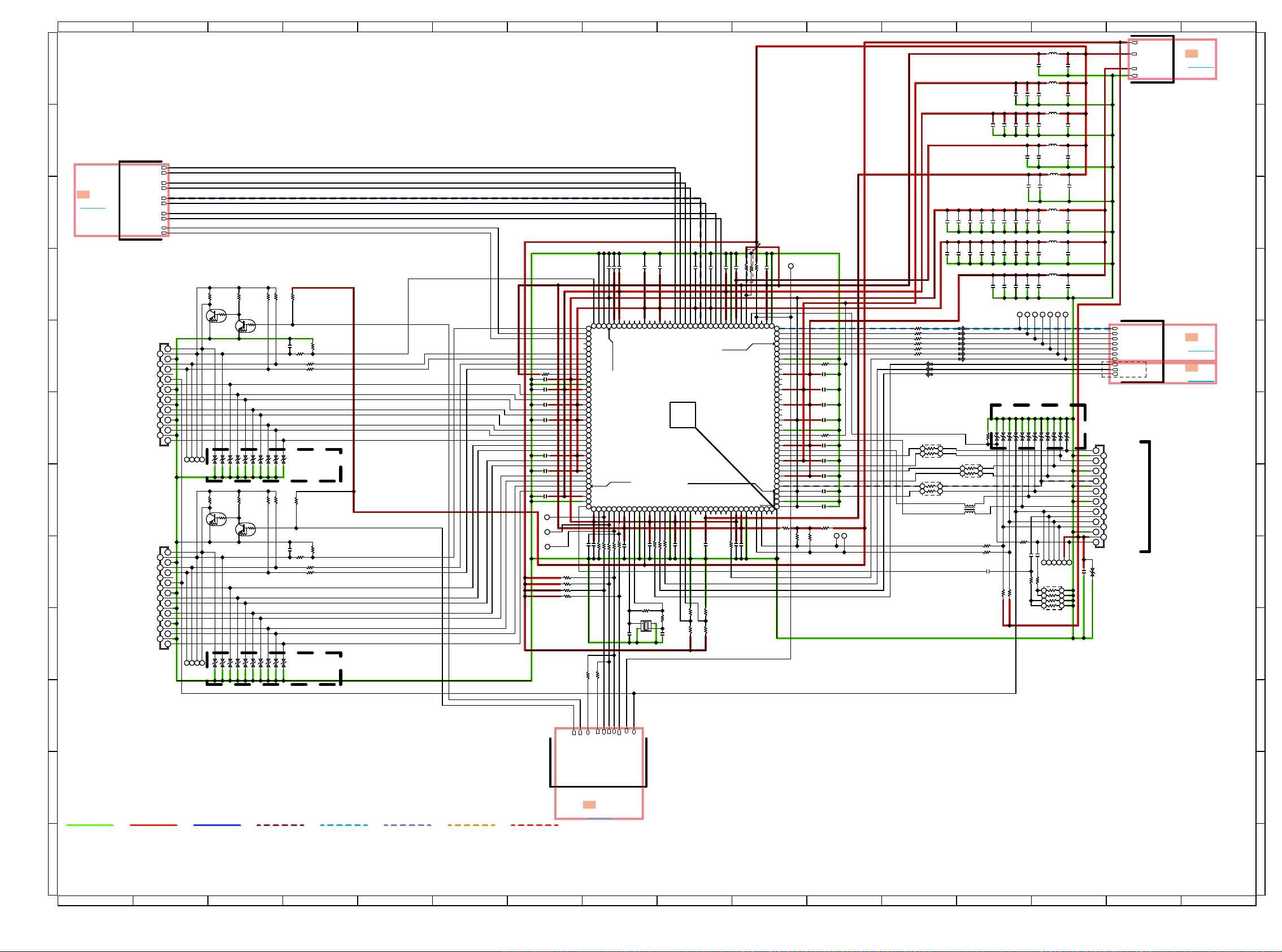
1
A
HDMI 4K PART
B
A7
TO 7A
C
FROM HDMI OSD PART
D
19.HP DET
HDMI_INPUT-4
HDMI_INPUT-5
18.+5V
17.GND
16.DDC DATA
15.DDC CLK
14.NC
13.CEC
12.CK-
11.D1 SHIELD
10.CK+
9.D0-
8.D1 SHIELD
BD(4K)
7.D0+
6.D1-
5.D2 SHIELD
4.D1+
3.D2-
2.D2 SHIELD
1.D2+
19.HP DET
18.+5V
17.GND
16.DDC DATA
15.DDC CLK
14.NC
13.CEC
12.CK-
11.D1 SHIELD
10.CK+
9.D0-
8.D1 SHIELD
GAME(4K)
7.D0+
6.D1-
5.D2 SHIELD
4.D1+
3.D2-
2.D2 SHIELD
1.D2+
E
F
G
H
J
2 3 4 5 6 7 8 9 10 11 12 13 14 15 16
HDMI_SDATA0
HDMI_SDATA1
HDMI_SDATA2
HDMI_SDATA3
HDMI_LRCLK
HDMI_SCLK
HDMI_MCLK
TXI2S0
TX64FS
TXFS
1.D2+
2
2.D2 SHIELD
3.D2-
4
4.D1+
5.D2 SHIELD
6
6.D1-
7.D0+
8
8.D1 SHIELD
9.D0-
10
10.CK+
11.D1 SHIELD
12
12.CK-
13.CEC
14
14.UTIL/HEAC+
15.DDC CLK
16
16.DDC DATA
17.GND
18
18.+5V
19.HP DET
CEC5V
CEC3V3
CEC1V1
DGND
HDMI_OUT
TXDDC_SDA
TXDDC_SCL
L7301
VDD33
AVDD33
AVDDH33
OPEN
C7352
C7353
PVDD33
TX2+
TX2-
TX1+
TX1-
TX0+
TX0-
TXC+
TXC-
* HDMI operation Countermeasure
10K
C7314
P3RXCP
P3RXCM
36.CH0ASD0
35.CH0ASD1
.CH0ASD2
34
33.CH0ASD3
4.VDD11
3.P1TX2P
2.VSS
1.VDD11
NC
NCNCCH0AMCLK
134
10K
0.1uF
0.1uF
OPEN
0.1uF
R7340
R7369
C7313
41
42
VSS
NTEST
PVDD33
TX1HPD
TX0HPD
AVDDH33
P0EXT_SWING
P1EXT_SWING
VDD11
VDD33
VSSNCTX1SCL
140
139
138
137
136
135
47
0.1uF
0.1uF
C7336
R7356
C7335
R7339
40
393837
NIRQA0
NIRQA1
CH0ALRCLK
CH0ABCLK
P0TXCM
AVDD11
P0TXCP
P0TX0M
AVDD33
P0TX0P
P0TX1M
AVDD11
P0TX1P
P0TX2M
VDD11
P0TX2P
P1TXCM
AVDD11
P1TXCP
P1TX0M
AVDD33
P1TX0P
P1TX1M
AVDD11
P1TX1P
P1TX2M
142
141
T7310
C7312
363534333231302928272625242322212019181716151413121110987654321
VSS
VDD33
VSS
VSS
144
143
R7357
OPEN
R7332
510 1%
C7311
1uF
C7310
1uF
0.
C7309
1uF
C7308
0.1uF
R7331
510 1%
C7307
1uF
C7306
0.1uF
C7305
1uF
C7304
0.1uF
C7303
0.1uF
R7360
0
1.8K
1.8K
T7311
R7359
R7358
T7312
JK724
CJJ9H021Z
JK725
CJJ9H021Z
0.1uF
0.1uF
0.1uF
C7319
C7320
C7321
1K
R7301
19
18
17
16
15
14
13
12
11
10
9
8
7
6
5
4
3
2
1
T7301
T7302
T7303
T7304
R7311
19
18
17
16
15
14
13
12
11
10
9
8
7
6
5
4
3
2
1
T7308
T7306
T7307
T7305
Q7301
RT1N141C
D7301
1K
Q7303
RT1N141C
D7311AAD7312
10K
47K
47K
R7303
R7304
R7323
47K
D7308AAD7309
AA
D7319
C7301
R7306 0
AA
ESD suppr
ASQS12U020R2
D7310
47K
R7314
C7302
R7316 0
AA
AA
ESD suppressor
ASQS12U020R2
D7320
OPEN
0.1uF
R7305
R7307 0
8 0
R730
OPEN
R7324
OPEN
0.1uF
R7315
R7317 0
R7318 0
OPEN
essor
7271706968
676665
RX0P5V
RX3SDA
RX3SCL
VDD33
P2RX2P
RX2SDA
C7329
OPEN
R7321
RX2SCL
RX1SDA
RX1SCL
RX0SDA
RX0SCL
CEC0
VDD11
VSS
AVDDH33
P1RXCM
P1RXCP
AVDD11
P1RX0M
P1RX0P
AVDD11
P1RX1M
P1RX1P
P1RX2M
P1RX2P
P0RXCM
P0RXCP
AVDD11
P0RX0M
P0RX0P
AVDD11
P0RX1M
P0RX1P
108 107 106 105 104 103 102 101 100 99 98 97 96 95 94 93 92 91 90 89 88 87 86 85 84 83 82 81 80 79 78 77 76 75 74 73
0.1uF
AVDDH33
70.VSS
69.VDD11
71.RX2P5V
72.RX1P5V
104.P0RX2M
105.P0RX2P
106.AVDDH33
107.VSS
108.TX1ARCIN
TX0ARCIN
HSCL0
VDD11
NIRQ1
NRESET
VDD33
HSDA0
115
114
113
112
111
110
109
47
47
1K
47K
0.1uF
R734447R7345
R7343
C7330
R7342
R7346
C7331
C7337
OPEN
R7322
47K
R7341
10K
C7322
0.1uF
0.1uF
C7323
C7324
0.1uF
C7325
0.1uF
C7326
0.1uF
C7327
0.1uF
C7328
0.1uF
T7309
7327
T
47K
I2C_SCL
T7328
I2C_SDA
R7347
R7348
R7349
R7320
OPEN
1000P
10K
10K
10K
R7302
Q7302
RT1N141C
AA
AA
AA
AA
D7302
D7306AAD7307
D7303AAD7304AAD7305
10K
R7313
R7312
Q7304
RT1N141C
AA
AA
AA
AA
AA
D7314
D7316AAD7317AAD7318
D7313
D7315
0.1uF
C7317
C7318
64
636261
60
P2RX0P
P2RX1P
AVDD11
P2RX0M
P2RX1M
P2RX2M
CVIMN864778
VSS
SYSCLK/XI
NC/XO
RX3P5V
VDD11
CH1ASD0
120
119
118
117
116
121
0.1uF
C7332
R730947R731047R7319
R7350
1M
X731
27MHz
15pF
C7338
595857
AVDD11
CH1ALRCLK
122
R7351
0.1uF
47
P2RXCP
P2RXCM
IC731
VSS
124
123
C7333
0
15pF
56
5554535251
P3RX2P
VDD11NCCH1ABCLK
126
125
0.1uF
P3RX2M
LPSA1
C7316
P3RX1P
P3RX1M
142.TX1SDA
143.TX0SCL
144.TX0SDA
VSS
LPSA0
128
127
R7352
3
R735
0.1uF
AVDD11
NC
129
10K
OPEN
0.1uF
C7315
50
49484746454443
P3RX0P
AVDD11
P3RX0M
NC
VDD33IO
132
131
130
C7334
0.1uF
10K
R7354
OPEN
R7355
133
R7338 33
R7337 33
R7336 33
R7335 33
R7334 33
R7333 33
RN731
RN733
12
12
0 ohm X 2
0 ohm X 2
VDD33IO
VDD11
AVDD11
34
34
C7369
C7379
OPEN
C7368
OPEN
C7378
AVDD11
RN732
EXC24CH9000U
OPEN
OPEN
12
0 ohm X 2
RN734
C7367
C7377
OPEN
C7366
OPEN
C7376
10K
R7368
34
R7361 0
R7362 0
C7339
OPEN
OPEN
C7365
OPEN
C7375
C7385
D7332
OPEN
C7364
OPEN
C7374
OPEN
C7384
ESD suppressor
ASQS12U020R2
D7331
A A
A A
1.8K
R7363
CB05YTYH221
C7342
C7343
OPEN
OPEN
C7345
C7346
C7347
OPEN
OPEN
OPEN
C7349
C7350
C7351
OPEN
C7355
C7356
OPEN
C7358
C7359
OPEN
OPEN
OPEN
C7361
C7362
C7363
OPEN
OPEN
OPEN
C7371
C7372
C7373
OPEN
OPEN
OPEN
C7382
C7383
C7381
T7315
T7314
T7313
4.7uF/6.3V
L7302
CB05YTYH221
4.7uF/6.3V
L7303
CB05YTYH221
4.7uF/6.3V
L7304
CB05YTYH221
4.7uF/6.3V
L7305
CB05YTYH221
4.7uF/6.3V
L7306
CB05YTYH221
4.7uF/6.3V
L7307
CB05YTYH221
4.7uF/6.3V
L7308
CB05YTYH221
4.7uF/6.3V
T7317
T7316
4.7uF/6.3V
C7344
4.7uF/6.3V
C7348
4.7uF/6.3V
C7354
4.7uF/6.3V
C7357
4.7uF/6.3V
C7360
4.7uF/6.3V
C7370
4.7uF/6.3V
C7380
4.7uF/6.3V
T7319
T7318
OPEN
D7329
D7324
D7328
D7327
D7326
D7325
D7323
D7322
D7330
A A
A A
A A
R7365
0
OPEN
C7340
OPEN
R7366
1.8K
R7364
D7321
JK726
A A
A A
A A
A A
A A
OPEN
C7341
T7323
T7322
T7321
R7367
OPEN
1234
RN735
OPEN
CJJ9H021Z
A A
A A
1
3
5
7
9
11
13
15
17
19
T7326
T7324
T7325
0.1uF
C7386
D7333
OPEN
A A
5678
MONITOR
FROM/TO DSP PART
9A
TO A9
TO DIGITAL POWER PART
A6
TO 6A
B0
TO 0B
A
B
C
D
E
F
G
H
J
K
L
M
GND LINE
1
POWER+ LINE
2 3 4 5 6 7 8 9 10 11 12 13 14 15 16
POWER- LINE
ANALOG AUDIO DIGITAL AUDIO TMDS SIGNAL ANALOG VIDEO STBY POWER
HPD4
HPD5
HDMI_SCL
MN864778_SCL
HDMI_SDA
MN864778_RST
MN864778_SDA
MN864778_HINT
MN864778_HAINT
FROM MCU PART
A3
TO 3A
K
CEC_COM
L
M
SCHEMATIC DIAGRAMS (3/12)
HDMI 4K
67
Page 68

1 2 3 4 5 6 7 8 9 10 11 12 13 14 15 16
A
B
C
D
E
F
G
H
J
K
L
CN741
TO CN781
DSP PART
*EMI Coutermeasure.
0.1uF
C7477
0.1uF
C7478
0.1uF
C7479
AD_RIN-
AD_RIN+
AD_LIN+
AD_LIN-
R7480
OPEN
AGND
R7481
OPEN
C7473
0.1uF
C7474
J7401
OPEN
J7402
J7403
J7404
D_SR-
D_SR+
D_SL+
D_SL-
D_SW-
D_SW+
D_CT+
D_CT-
D_FR-
D_FR+
D_FL+
D_FL-
+5VA
CBL/SAT
JK784
COAX
OPTION
CN741
1.+12V
2.VGND
3.-12V
4.CVBS_SW2
5.CVBS_SW5
6.+5VD
7.OPT1_IN
8.DGND
9.OPT2_IN
FFC WAFER/9P/1.0mm
TO VIDEO/OPTICAL PART
1
2
3
4
5
6
7
8
9
3B
TO B3
FROM/TO INPUT/VOLUME PART
AD_LIN-
AD_LIN+
AD_RIN+
AD_RIN-
D_FL-
D_FL+
D_FR+
D_FR-
D_SW-
D_CT-
D_CT+
D_SW+
D_SL-
D_SL+
D_SR+
D_SR-
DA_GND1
DSP_AUDIO
100
100
R7478
R7477
100P
0.1uF
C7449
+5VD
C7450
0.1uF
C7452
0.1u
C7453
100/63V
D_SBR-
D_SBR+
D_SBL+
*SOUND QUALITY Coutermeasure.
D_SBL-
L7403
OPEN
*SOUND QUALITY Coutermeasure.
+5VD
100P
C7816
R7811
S500BTE3
JK784
C7816
100pF 0.1uF
R7811
F
C7454
* Cirrus Recommend
75
D7803
C7448
4.7uF/100V
C7451
VQ
17
AINR-
FILT+
18
RESET
REFGND
19
AOUTB4-
20
16.AINL-
15.AINL+
14.AINR+
AOUTB4+
21
AOUTA4+
22
AOUTA4-
23
CS42528-CQ
VA
24
DIR + CODEC
AGND
25
AOUTB3-
26
AOUTB3+
27
AOUTA3+
28
33.AOUTA2-
34.AOUTB1-
AOUTA3-
29
AOUTB2-
30
AOUTB2+
31
AOUTA2+
AOUTA1+
AOUTA1-
32
33 34 35 36 37 38 39 40 41 42 43 44 45 46 47 48
0.1uF
470/50V
C7455
C7727
OPEN
C7456
L7404
C7458
FCM601T05
OPEN
S500BTE1C/
X510BTE1/E1C
XO
XO
A
DIR_INT
CODEC_MUTE
C7436
0.1uF
C7435
0.1uF
+3V3D
C7434
DSP_MODE_SEL
DIR_CE
DIR_RST
DIR_MOSI
DIR_CLK
DIR_MISO
HDMI_SW
DSP_CS
DSP_PCP_BSY
DSP_RST
DSP_MOSI
DSP_MISO
DSP_CLK
HDMI2_SW
RN751
1234
RN750
1234
15P
AD[0:19]
A2
DSP_SPC1_IRQ
TO 2A
B
FROM/TO MCU PART
C
D
DA7
5678
DA6
DA5
33X4
33X4
DA4
E
DA3
5678
DA2
DA1
DA0
SD3
R7430
SD6
75
SD7
AD9
AD8
AD7
AD6
AD5
AD4
F
G
H
J
K
4B
TO B4
TO DIGITAL POWER PART
AGND
+5VA
DGND
VGND
R7479
* Cirrus Recommend
+5VD
OPEN
C7447
C7728
LRCK1
SCLK1
CX_SDIN2
INT
35.AOUTB1+
MUTEC
1000P
0.1uF
VD
CX_SDIN3
VLC
DGND
AD0/CS
LPFLT
R7412
C7457
AD1/CDIN
IC744
CX_SDIN4
SCL/CCLK
SDA/CDOUT
SAI_SCLK
SAI_LRCK
2.CX_SCLK
3.CX_LRCK
1.CX_SDIN1
OMCK
ADCIN1
ADCIN2
CX_SDOUT
RMCK
SAI_SDOUT
46.RXP3/GPO3
47.RXP2/GPO2
48.RXP1/GPO1
DGND
RXP0
VARX
RXP6/GPO6
AGND
RXP7/GPO7
RXP5/GPO5
RXP4/GPO4
0.01uF
0.1uF
0.01uF
0.1uF
0.1uF
OPEN
1
C7464
C7463
C7462
C7460
C746
1.37K(1%)
0.022uF
100uF/10V
C7459
+5VD
OPEN
C7446
0.1uF
100uF/10V
12345678910111213141516
64
63
62
SCLK2
61
LRCK2
60
59
58
57
SDTO1
56
MCKO
55
SDTO2
54
VLS
53
52
VD
51
TXP
50
49
0.01uF
0.1uF
C7466
C7467
C7465
DGND
+3V3D
+1V8H
*SOUND QUALITY Coutermeasure.
C7442
CB05YTYH221
100/50V
C7443
L7401
0.1uF
C7444
C7445
0.1uF
R7476
R7475
R7474
R7473
R7472
R7471
+5VD
100uF/10V
R7482
R7483
C7475
C7476
C7480
L : A OUT(HDMI off)
H : B OUT( HDMI on)
GND3Y
9 10 11 12 13 14 15 16
100uF/10V
1K
C7469
C7468
OPEN
C7438
OPEN
C7439
C7440
OPEN
C7441
OPEN
OPEN
C7472
100
33
1K
220
33
C7471
0.1uF
0.1uF
C7470
100uF/10V
0
0
OPEN
OPEN
0.1uF
2B
2A
2Y
3B
3A
4Y
100
R7449
*HDMI SPDIF MODE : DIR MASTER
*HDMI I2S MODE : HDMI MASTER
*ADC MODE : DSP MASTER
*DIR MODE : DIR MASTER
12345678
1A
1B
1Y
4B
4A
ST
C7437
0.1uF
* Cirrus Recommend
R7424, R7425: 10K-->3.3K Change.
100
R7423
127
GNDD6
SCP1/PCP_BSY
I1_DATA1,DSD1
DAO2_D1,HS4
DAO_MCLK
40
4A
1B
3.3K
3.3K
R7422
C7426
125
126
VDD6
SCP1_CLK
TEST
VDD1
4142434445
C7410
OPEN
R7409
4B
1Y
R7420
+3V3D
0.1uF
121
122
123
124
GNDIO6
RESET#
SCP1_MOSI
SCP1_MISO/SDA
1.SCP2_CK
2.SCP2_MISO
3.SCP2_MOSI
4.SCP1_IRQ
35.DAO2_D3
36.DBDA
37.DBCK
38.DAO2_D2
GNDD1
DAO2_D0,HS3
DAO2_SCLK
DAO2_LRCLK
46
0.1uF
OPEN
OPEN
RN743 33X4
R7410
R7411
4Y
2A
100P
C7425
0.1uF
C7424
C7423
100uF/10V
114
115
116
117
119
118
120
GND5
VDDIO6
EXT_A17
EXT_A19
EXT_A18
EXT_OE#
EXT_CS1#
IC741
AUDIO DSP
CS497024CVZ
GNDIO1
VDDIO1
DAO1_DATA1,HS1
DAO1_D2,HS2
DAO1_D3
DAO1_DATA0,HS0
DAO1_SCLK
47
48
49
50
5152535455
0.1uF
C7412
5 6 7 8
1 2 3 4
3A
2B
10K
R7414
100
R741633R7413
910111213141516
3B
3YGND
2Y
SD[0:7]
SD5
SD0
SD1
5 6 7 8
33X4
RN747
1 2 3 4
C7422
0.1uF
109
110
111
112
113
VDD5
SD_CS#
EXT_A15
EXT_A16
SD_RAS#
102.SD_A0,EXT_A0
101.SD_A1,EXT_A1
100.VDDIO5
99.SD_A2,EXT_A2 SD_A4,EXT_A4
68.SD_D0,EXT_D0
67.GNDIO2
66.EXT_WE#
65SD_D1,EXT_D1
SD_D7,EXT_D7
GND2
SD_DQM0
VDD2
DAO1_LRCLK
56
57585960616263
0.1uF
C7414
R7415
10K
DA15
DA14
SD2
AD0
AD1
AD13
5 6 7 8
33X4
RN746
1 2 3 4
+3V3D
106
103
104
105
107
108
GNDIO5
SD_WE#
SD_CAS#
SD_A10,EXT_A10
SD_BA1,EXT_A14
SD_BA0,EXT_A13
GNDD4
SD_A3,EXT_A3
VDD4
EXT_CS2#
SD_A5,EXT_A5
GNDIO4
SD_A6,EXT_A6
SD_A7,EXT_A7
VDDIO4
SD_A8,EXT_A8
SD_A9,EXT_A9
GND3
SD_A11,EXT_A11
SD_A12,EXT_A12
VDD3
SD_CLKEN
SD_CLKIN
SD_CLKOUT
SD_DQM1
SD_D8,EXT_D8
SD_D9,EXT_D9
GNDIO3
SD_D10,EXT_D10
SD_D11,EXT_D11
VDDIO3
SD_D12,EXT_D12
SD_D13,EXT_D13
SD_D14,EXT_D1
SD_D15,EXT_D15
SD_D2,EXT_D2
SD_D3,EXT_D3
SD_D4,EXT_D4
SD_D5,EXT_D5
SD_D6,EXT_D6
VDDIO2
C7415
0.1uF
DA13
DA12
DA11
DA10 AD12
C7420
0.1uF
C7419
0.1uF
C7418
0.1uF
C7417
0.1uF
R7419
33
R7418
33
C7416
0.1uF
4
65 66 67 68 69 70 71 72 73 74 75 76 77 78 79 80 81 82 83 84 85 86 87 88 89 90 91 92 93 94 95 96 97 98 99 100 101 102
64
+3V3D
IC746, IC747 CONTROL
L : A OUT(ADV7623_I2S)
H : B OUT(MN864778_I2S)
C7482
0.1uF
4B
4A
ST
VCC
IC747
SEL
1A
1B
TC74VHC157FT
1 2 3 4 5 6 7 8
1Y
AD[0:19]
C7429
IC743
M12L16161A5TG2Q
100uF/10V
RN748
RN749
+3V3D
5678
1234
33X4
1234
5678
RN745
33X4
AD2
AD3
DA8
AD4
DA9
AD5
1 2 3 4
5 6 7 8
RN744
33X4
1 2 3 4
5 6 7 8
DA10
DA11
AD6
AD7
AD8
DA12
AD9
DA13
DA14
DA15
33X4
SD7
SD6 SD4
SD2
SD3
DA0
SD1
DA1
SD0
DA2
SD5
DA3
DA4
DA5
DA6
DA7
DA8
DA9
AD13
AD12
AD0
AD1
AD2
AD3
R7417
33
DA[0:15]
910111213141516
3B
3A
4Y
2A
2B
2Y
GND 3Y
SD4
C7430
C7431
0.1uF
C7432
0.1uF
C7433
0.1uF
0.1uF
512K * 16Bit * 2Banks
50
VDD
VSS
494847464544434241403938373635343332313029282726
DQ0
DQ15
DQ1
DQ14
VSSQ
VSSQ
DQ2
DQ13
DQ3
DQ12
VDDQ
VDDQ
DQ4
DQ11
DQ5
DQ10
VSSQ
VSSQ
DQ6
DQ9
DQ7
DQ8
VDDQ
VDDQ
LDQM
NC
_WE
UDQM
_CAS
CLK
_RAS
CKE
_CS
NC
BA
A9
A10/AP
A8
A0
A7
6
A1
A
A5
A2
A4
A3
25 24 23 22 21 20 19 18 17 16 15 14 13 12 11 10 9 8 7 6 5 4 3 2 1
VSSVDD
+3V3D
10K
3.3K
10K
R7428
R7426
24.576MHz
X741
10pF
C7403
C7428
1M
R7403
C7404
1 2 3 4
CEVDD
0.1uF
+3V3D
L7402
CB05YTYH221
10pF
220/10V
C7405
R7427
SOHOLD
WPSCK
VSSSI
IC742
5678
MX25L8006EM2I-12G
10K
R7429
R7401
3.3K
10KX4
RN741
1 2 3 4
5 6 7 8
RN742 10KX4
1 2 3 4
5 6 7 8
330
R7402
1uF
0.01uF
C7406
C7407
R7406
+3V3D
C7401
5.1K(1%)
C7408
C7409
R7405
3.3K
R7407
10K
R7408
10K
+3V3D
0.1uF
C7402
0.1uF
R7404
0.1uF
0.1uF
+3V3D
3.3K
3.3K
R7425
R7424
+1V8
C7427
100uF/10V
128
1234567891011121314151617181920212223242526272829303132333435363738
PCP/SCP2_IRQ#
SCP1_CS#
PCP/SCP2_CS#
VDDIO7
GNDIO7
GPIO3,DDAC
GPIO2,UART_TXD
VDD7
GPIO1,UART_RXD
GPIO1,UART_CLK,EE_CS#
GND7
XTAL_OUT
XTI
XTO
GNDA
PLL_REF_RES
VDDA(3.3V)
VDD8
DAI1_DATA3,DSD3
DAI1_DATA2,DSD2
GND8
DA
DAI1_DATA0,DSD0
VDDIO8
DAI1_SCLK,DSD-CLK
DAI1_LRCK,DSD4
GNDIO8
DAI2_LRCK
DAI2_SCLK
DAI2_DATA,DSD5
3.3K
39
*HDMI AUDIO Countermeasure
R7447
100
SEL
IC745
VCC
TC74VHC157FT
R7448
68
R7484
OPEN
68
68
R7432
R7443
R743168R744468R744568R7446
68
C7481
0.1uF
ST
VCC
IC746
1A
SEL
TC74VHC157FT
1 2 3 4 5 6 7 8
L
M
GND LINE
-12V
POWER+ LINE
VGND_1
TO INPUT/VOLUME PART
2B
TO B2
POWER- LINE
+12V
ANALOG AUDIO DIGITAL AUDIO TMDS SIGNAL ANALOG VIDEO STBY POWER
CVBS_SW2
CVBS_SW5
FROM DSP PART
A5
TO 5A
I_SDATA0
HDMI_SCLK
HDMI_MCLK
HDMI_LRCLK
HDMI_SDATA3
HDMI_SDATA2
HDMI_SDATA1
HDM
0B
TO B0
FROM/TO HDMI 4K PART
TXI2S0
TXFS
TX64FS
HDMI2_SDATA0
1B
HDMI2_SDATA1
HDMI2_SDATA2
TO B1
HDMI2_SCLK
HDMI2_MCLK
HDMI2_LRCLK
HDMI2_SDATA3
FROM/TO HDMI OSD PART
M
SCHEMATIC DIAGRAMS (4/12)
DSP
1
2 3 4 5 6 7 8 9 10 11 12 13 14 15 16
68
Page 69

1
A
B
C
DV5_POWER
D
E
CEC_POWER
F
G
H
DV5_POWER
J
K
USB_POWER1
L
2 3 4 5 6 7 8 9 10 11 12 13 14 15 16
A8
TO 8A
DV3V3
CEC5V
D1V8H
DGND
CN751
OPEN
C7508
C7507
* P_DOWN COUNTERMEASURE
Q7511
OPEN
R7538
OPEN
R7539
0.1uF
0.1uF
0.1uF
0.1/50V
OPEN
C7576
C7577
C7575
C7592
C7593
*EMI Coutermeasure.
ET751
OPEN
CB03YTYH600
L7501
CB03YTYH600
L7502
CB03YTYH600
OPEN
OPEN
L7521
C7506
C7505
470uF/16V
R7541
R7540
OPEN
C7542
0.1uF
C7784
CB03YTYH600
C7594
D7503
1SS355T
OPEN
C7504
CB03YTYH600
OPEN
L7129
IC755
CB03YTYH600
PST8448NR
51
CDVOUT
C7551
VDD
0.015uF
2
0.1uF
1uF
0.01uF
C7787
C7785
C7786
MCU+5V MCU+3V3
NJM2845DL133
C7578
C7579
0.1uF
100uF/16V
L7503
0.1uF
0.1uF
0.1uF
C7501
C7502
C7503
470uF/16V
MAIN_POWER
R7543
MCU+3V3
10K
10K
D7501
R7542
1SS355T
4
1uF
C7544
NC
R7544
GND
4.7K
3
1SS355T
D7502
0.01uF
IC756
31
IN
OUT
GND
C7580
2
0.22uF
100K
R7545
R7546
Q7512
2SC3052
100
47K
0.1uF
C7543
R7547
C7581
220uF/16V
R7548
10K
C7545
Q7513
ISA1530AC1
RT1N141C
Q7515
OPEN
R7549
Q7514
0.1uF
SWM3.3V
3.3K
L7429
CB03YTYH600
CJP05GI289ZY
54321
5.D5.2V
4.D5.2V
3.D_GND
2.D_GND
1.MAIN_POWER
DSP_POWER
MAIN_POWER
CPU_POWER
CEC_POWER
CEC_POWER2
DV5_POWER
DA_POWER
USB_POWER1
USB_POWER2
DV_POWER
POWER_DOWN
MCU+5V
MCU+3V3
MCU_RST
SWM3V3
DGND
SWM5V
D5V
USB3V3
USB_POWER1/USB1V2
CN751
TO BN601
WAFER/5P/2.5mm
FROM/TO SMPS B'D
A1
TO 1A
FROM/TO MCU PART
SWM5V
R7551
CPU_POWER
CEC_P
USB_POWER1
OPEN
D7504
R7552 0
OWER2
R7559
OPEN
R7560 0
C7582
L7522
OPEN
C7583
OPEN
OPEN
* USB1V2 / USB_POWER1 OPTION
R7550
OPEN
OPEN
Q7516
OPEN
+5VD
+3V3D
N
C7584
C7585
OPEN
OPE
R7561
0
5V1H
D7105
C7595
C7145
0.1uF
0.1uF
47K
C7140
R7192
OPEN
5V1H
D7106
+1V8H
+5VA
AGND
DA_GND2
USB/BT_L
USB/BT_R
MIC_SIGNAL
CN752
1.+5VA
2.DA_GND
3.USB/BT_R
4.DA_GND
5.USB/BT_L
6.AGND
7 6 5 4 3 2 1
7.MIC_SIGNAL
DGND
B4
TO 4B
TO DSP PART
FROM/TO INPUT/VOLUME PART
5B
TO B5
CN752
TO BN914
TO USB/BT B'D
WAFER/7P/2.0mm
*EMI Coutermeasure.
DIGITAL POWER PART
*EMI Coutermeasure.
L7506
CB05YTYH221
R7506
L7507
76.8K 1%
OPEN
0
348K 1%
R7505
22uF/6.3V
C7514
R7511
300k 1%
R7512
39K 1%
10uF/6.3V
22uF/6.3V
C7558
C7559
174K 1%
0
10uF/6.3V
22uF/6.3V
C7569
C7570
OPEN
OPEN
OPEN
OPEN
C7537
C7536
10uF/6.3V
OPEN
C7515
C7516
*EMI Coutermeasure.
L7511
CB05YTYH221
L7512
OPEN
OPEN
C7560
*EMI Coutermeasure.
L7515
CB05YTYH221
L7516
OPEN
OPEN
C7571
L7519
OPEN
L7520
OPEN
OPEN
C7538
C7517
0.1uF
OPEN
C7562
C7561
0.1uF
OPEN
C7572
C7573
OPEN
OPEN
C7540
C7541
C7539
100K
R7502
C7509
R7501
0.1uF
33
L7504
CB03YTYH600
L7505
OPEN
C7510
0.1uF
HDMI 4K
100K
C7553
R7508
0.1uF
R7507
33
C7554
L7509
CB03YTYH600
L7510
OPEN
0.1uF
R7509
HDMI OSD
100K
R7514
C7564
0.1uF
R7515
R7513
33
CB03YTYH600
C7565
L7513
L7514
OPEN
0.1uF
100K
USB(BX8804)
R7520
C7531
OPEN
OPEN
R7521
OPEN
L7517
L7518
OPEN
OPEN
X7R Series
R7519
OPEN
C7532
OPEN
1uF
C7513
AGND
AVIN
NC
VFB
IC752
123
AGND
IC753
PGND
16
1718192021222324
IC751
CVIEN5339QI
123
NC(SW)
AGND
VFB
PGND
PGND
VFB
ND
PG
NC
VFB
PGND
VOUT
TST0
131415
TST1
3.3P
C7512
TST2
PGND
PGND
VOUT
VOUT
VOUT
5 6 7 8 9 10 11 12
4
PGND
PGND
VOUT
NC
3
TST0
141516
1
TST1
TST2
PGND
PGND
VOUT
VOUT
VOUT
5 6 7 8 9 10 11 12
4
VOUT
NC
TST0
131415
TST1
TST2
PGND
PGND
VOUT
VOUT
VOUT
5 6 7 8 9 10 11 12
4
VOUT
R7504
5P
C7556
R7510
348K 1%
R7517
5P
C7567
R7516
348K 1%
R7518
USB1V2
TST0
131415
TST1
OPEN
C7534
TST2
PGND
PGND
VOUT
VOUT
VOUT
5 6 7 8 9 10 11 12
4
OPEN
R7522
R7523
POK
R7503
100K
ENABLE
PVIN
PVIN
NC(SW)
NC(SW)
NC(SW)
NC(SW)
C7511
10uF/6.3V
1uF
C7557
AVIN
POK
1718192021222324
100K
ENABLE
PVIN
PVIN
NC(SW)
NC(SW)
CVIEN5339QI
NC(SW)
NC(SW)
C7555
10uF/6.3V
X7R Series
X7R Series
NC(SW)
1uF
C7568
AVIN
POK
16
1718192021222324
ENABLE
PVIN
PVIN
NC(SW)
NC(SW)
CVIEN5339QI
NC(SW)
NC(SW)
123
C7566
NC(SW)
10uF/6.3V
OPEN
C7535
AGND
AVIN
POK
16
1718192021222324
ENABLE
PVIN
PVIN
IC754
NC(SW)
OPEN
NC(SW)
NC(SW)
NC(SW)
123
OPEN
C7533
PGND
NC(SW)
D3.3V
0.1uF
OPEN
C7518
CEC1V1
OPEN
C7563
D1.8V
OPEN
C7574
A9
TO 9A
TO HDMI 4K PART TO HDMI OSD PART
CEC3V3
CEC5V
DGND
CEC1V1
L7508
Q7522
TPC6111
3 2 1
0.1uF
C7549
3 2 1
0.1uF
C7597
3 2 1
0.1uF
C7523
3 2 1
0.1uF
C7588
CB03YTYH600
OPEN
OPEN
OPEN
C7521
C7520
C7591
C7522
0.1uF
654
Q7502
TPC6111
C7550
0.1uF
654
Q7503
TPC6111
C7598
0.1uF
654
Q7506
TPC6111
C7524
0.1uF
654
Q7520
TPC6111
C7589
0.1uF
L7523
OPEN
L7527
CB03YTYH600
DA_POWER
C7519
OPEN
DA_POWER
CEC_POWER
CEC_POWER
CEC_POWER
Q7521
RT1N441C
10K
R7557
R7558
10K
Q7501
RT1N441C
Q7504
RT1N441C
R7529
Q7505
RT1N441C
R7555
Q7519
RT1N441C
3 2 1
C7590
10K
R7524
R7525
10K
10K
R7527
R7526
10K
R7530
10K
10K
R7556
10K
654
0.1uF
10K
* HDMI OSD D1V8H OPTION
L7525
L7526
OPEN
L7524
OPEN
CB03YTYH600
DV_POWER
DSP_POWER
Q7507
RT1N441C
Q7517
RT1N441C
3 2 1
0.1uF
C7525
3 2 1
0.1uF
C7586
654
C7526
0.1uF
Q7508
TPC6111
654
Q7518
TPC6111
C7587
0.1uF
10K
R7531
R7532
10K
10K
R7553
R7554
10K
* DSP +1V8H OPTION
USB_POWER2
Q7509
RT1N441C
10K
R7533
R7534
10K
3 2 1
0.1uF
C7527
654
Q7510
C7528
0.1uF
TPC6111
A
B
C
D
E
F
G
H
J
K
L
M
GND LINE
1
POWER+ LINE
2 3 4 5 6 7 8 9 10 11 12 13 14 15 16
POWER- LINE
ANALOG AUDIO DIGITAL AUDIO TMDS SIGNAL ANALOG VIDEO STBY POWER
M
SCHEMATIC DIAGRAMS (5/12)
DIGITAL POWER
69
Page 70

1 2 3 4 5 6 7 8 9 10 11 12 13 14 15 16
A
B
C
D
E
F
G
H
J
K
TU771
1.CH_GND
2.INT
3./RST
4./CE
5.SDIO
6.SCLK
7.VCC
8.R-OUT
TO BN508
9.L-OUT
FROM TUNER MODULE
CBL/
SAT IN
MEDIA
PLAYER IN
SW1
PRE OUT
SUBWOOFER
L CH
R CH
L CH
R CH
SW2
TU771
JK771
INPUT/VOLUME PART
MCU+3V3
AGND
SUB_MUTE
DGND
DAC_MUTE
MAIN_VOL_CLK
A4
R7774
0
T7607
T7609
T7608
MAIN_VOL_DATA
TUNER_INT
TUNER_RST
TUNER_CE
TUNER_SDIO
TUNER_SCLK
+12V
-12V
-12V
+12V
VGND_1
CN771
1.DA+5V
1234567
2.DA_GND
3.+12V
4.AGND
5.-12V
6.RLY_GND
7.VGND(RET_GND)
+5VA
AGND
DA_GND2
USB/BT_L
USB/BT_R
MIC_SIGNAL
CN772
13121110987654321
13.DGND
12.MUTE_+B
11.RLY_GND
10.+12V
9.FR
8.AGND
7.SR
6.AGND
5.CEN
4.AGND
3.SL
2.AGND
1.FL
TO 4A
B2
TO 2B
CN771
B5
TO 5B
CN772
R7637 100
R7651 100
100P
C7611
27K
0.1uF
0.1uF
1M
R7617
1M
R7618
1M
R7621
1M
R7622
OPEN
0.1uF
C7612
470/16V
Q7610
INC2001AC1
100P
100P
100P
C7613
C7610
C7614
L7601
CB03YTYH600
R7605
0
R7606
0
0.1uF
C7622
0.1uF
C7738
R7625
470
R7757
0.1uF
C7739
12K
C7707
R7653 100
R7656 100
R7657 100
Q7611
OPEN
AGND
C7709
100uF/16V
0.1uF
R7758
10K
R7638
470
R7626
10K
R7641
OPEN
C7643
22uF/50V
R7728
100
R7639
100
R7640
OPEN
C7634
C7633
OPEN
*SOUND QUALITY Coutermeasure.
0.1uF
*EMI Coutermeasure.
0.1uF
C7735
1uF
0.01uF
C7741
C7740
R7772
R7762
OPEN
R7773
OPEN
0
R7763
C7640
0
OPEN
ET761
OPEN
OPEN
R7766
DA_GND1
RLY_GND
*EMI Coutermeasure.
0.1uF
0.1uF
0.1uF
C7641
C7732
C7733
OPEN
R7721
OPEN
OPEN
OPEN
R7759
R7767
R7760
0.01uF
C7743
MUTE_+B
C7742
CB03YTYH600
FR
AGND
SR
AGND
C
AGND
SL
AGND
FL
T7606
T7602
T7605
T7604
T7603
T7601
D7601
ZJ7.5VBT
R7736
150(1W)
100/63V
100/63V
D7602
ZJ7.5VBT
R7665 470
R7664 470
R7666 47
R7668 470
R7667 470
C7696
0
R771
R7702
OPEN
C7713
OPEN
C7716
R7737
150(1W)
0
Q7606
OPEN
123
R7716
OPEN
OPEN
C7699
100K
R7714
10uF/100V
IC764
NJM8080G
100
R7724
330P
C7694
3K(0.5%)
2K
R7711
C7693
0.1uF
C7691
1500P
C7689
330P
2K
C7687
R7708
1500P
R7706
3K(0.5%)
R7703
C7685
2.4K(0.5%)
1500P
D_SL-
D_SL+
R7717
4 5 6
OPEN
C7700
R7715
100K
C7698
0.1uF
A OUTPUT
8765
V+
B OUTPUT
A
- +
A-INPUT
C7695
B
-+
A+INPUT
B-INPUT
R7713
V-
4 3 2 1
B+INPUT
C7692
1500P
C7690
330P
C7688
R7709
1500P
R7707
3K(0.5%)
R7704
C7686
2.4K(0.5%)
2.4K(0.5%)
1500P
D_SR+
C7630
R7635 OPEN
R7636 OPEN
C7646
R7608
C7720
10uF/100V
C7721
10uF/100V
100uF/50V
0
DSP_AUDIO
100K
R7633
C7648
100uF/50V
R7632 OPEN
100K
R7634
TUNER_L
TUNER_R
DCAP_4
26 25 24 23 22 21 20 19 18 17 16 15 14
27
R4IN
L2IN
28
L4IN
29
SAT_R
30
SAT_L
31
R6IN
NJU72340AFH3
32
L6IN
33
DVD_R
34
DVD_L
35
DCAP_5
36
MONOIN
DCAP_6
37
ADC_R
38
ADC_L
C_C
39
DAC_FR
DAC_FL
DA
AGND
Q7604
OPEN
R7684
C7666
R7682
10uF/100V
C7663
IC762
100
R7726
C7661
R7678
3K(0.5%)
R7679
C7658
1500P
2K
R7676
R7670
C7652
2.4K(0.5%)
1500P
D_FL-
R7628 OPEN
R7631 OPEN
R2IN
IC761
DAC_SL
OPEN
OPEN
NJM8080G
330P
2K
0.1uF
C7656
330P
C7654
1500P
R7674
3K(
0.5%)
R7671
2.4K(0.5%)
D_FL+
C7631
OPEN
OPEN
C7649
100uF/50V
R7643
R7642
R7629 OPEN
DCAP_3
REC_L
REC_R
13
CLOCK
12
DATA
AGND
MINI_L
MINI_R
11
AGND
SBL_IN2
SBR_IN2
C7650
10
DCAP_2
100uF/50V
9
DCAP_1
8
SW OUT
7
SBR OUT
6
SBL OUT
5
SR OUT
4
SL OUT
3
C OUT
2
FR OUT
FL OUT
DAC_SR
R7609 OPEN
100K
A-INPUT
A+INPUT
4 3 2 1
C7660
1
DAC_SBL
DAC_SBR
DAC_SW
52515049484746454443424140
AVEE
AVCC
DCAP_7
DCAP_8
100uF/50V
C7608
100uF/50V
C7609
R7610 OPEN
123
R7685
A
C7667
R7683
C7665
B OUTPUT
B
-+
B-INPUT
B+INPUT
C7657
C7655
R7675
3K(0.5%)
0.1uF
V+
C7659
1500P
330P
1500P
OPEN
OPEN
100K
C7664
10uF/100V
8765
100
R7725
330P
C7662
R7680
3K(0.5%)
2K
R7681
2K
R7677
R7673
R7672
C7653
2.4K(0.5%)
2.4K(0.5%)
1500P
D_FR-
D_FR+
4 5 6
A OUTPUT
- +
V-
0.1uF
C7647
0.1uF
C7651
Q7605
OPEN
123
R7700
OPEN
OPEN
C7683
100K
R7698
10uF/100V
IC763
C7680
NJM8080G
100
R7719
330P
C7678
R7694
3K(0.5%)
2K
R7695
C7676
0.1uF
C7674
1500P
C7672
330P
2K
C7670
R7692
1500P
R7690
3K(0.5%)
R7686
R7687
C7668
2.4K(0.5%)
2.4K(0.5%)
1500P
D_CT+
D_CT-
R7701
A
C7684
R7699
C7682
0.1uF
V+
B OUTPUT
B
-+
B-INPUT
B+INPUT
C7675
4700P
C7673
1000P
C7671
4700P
R7691
8.2K(0.5%)
OPEN
OPEN
100K
C7681
10uF/100V
8765
100
R7718
1000P
C7679
R7696
8.2K(0.5%)
2K
R7697
2K
R7693
R7688
R7689
C7669
2.4K(0.5%)
2.4K(0.5%)
1500P
D_SW-
D_SW+
4 5 6
A OUTPUT
- +
A-INPUT
A+INPUT
V-
4 3 2 1
USB/BT_R
R7775
0
R7776
0
R7777
0
R7778
0
USB/BT_L
AD_LIN+
R7649
MCU+3V3
D7605
D7607
D7606
1SS355T
1SS355T
1SS355T
10K
820
R7650
R7652
D7608
ZENER(3.6V/0.5W)
10K
DGND
OPEN
100
AGND
C7644
0.1/50V
470K
R7647
R7648
1K
Q7613
RT1N441C
15K
150K
OPEN
R7729
R7727
4.7K
220P
R7752
C7710
C7712
100
R7753
AD_LIN-
22uF/50V
5678
0.1uF
Q7612
RT1P441C
Q7614
C7627
R7754
4.7K
+
-
CM2
+
CM1
IC767
NJM2115MTE1
C7617
2700P
C7645
RT1P441C
-
1 2 3 4
R7730
R7755
10uF/50V
0
4.7K
C7711
R7756
R7722
OPEN
C7734
MUTE_+B
AGND
SR
AGND
SL
AGND
C
AGND
FR
AGND
FL
AGND
Q7608
OPEN
C7697
10uF/100V
100
R7723
330P
R7712
3K(0.5%)
2K
2K
R7705
2.4K(0.5%)
D_SR-
OPEN
OPEN
R7735
OPEN
OPEN
C7717
R7734
Q7609
OPEN
0.1uF
0.1uF
C7618
C7615
13
2
46
57
8
9
CHGND
JK772
150K
R7732
R7627
CHGND
CHGND
C763
0.1uF
R7764
CHGND
15K
R7742
220P
C7704
100
R7745
AD_RIN-
*SOUND QUALITY Coutermeasure.
R7601
270
R7602
270
OPEN
R7658
0
C7703
0.1uF
R7614
8
D7603
OPEN
D7604
OPEN
OPEN
R7765
OPEN
OPEN
R7743
4.7K
R7744
C7705
0.1uF
R7659
DGND
R7654
R7740
R7615
R7616
100
R7619
R7620
100
R7655
R7738
C7702
OPEN
220
C7639
C7629
22uF/50V
R7611
5678
-
CM2
IC766
NJM2115MTE1
C7706
2700P
OPEN
OPEN
OPEN
100
100
0
0
4.7K
+
+
R7603
C7642
22uF/50V
100K
330P
R7623
R7741
-
CM1
1 2 3 4
C7607
C7605
0.1uF
27K
R7604
C7621
0.1uF
C7737
C7736
*EMI Coutermeasure.
220P
C7619
220P
C7620
220P
C7623
220P
C7624
100K
R7624
0
4.7K
R7747
C7708
100
R7748
AD_RIN+
FROM MCU PART
TO DSP PART
TO BN301
TO REGULATOR B'D
FROM/TO DIGITAL POWER PART
TO BN501
TO MAIN B'D
WAFER/13P/2.0mm
A
B
C
D
WIRE/7P/2.5mm
E
F
G
H
J
K
L
M
GND LINE
L
T+
D_FL-
D_FL+
AD_LIN-
AD_RIN-
AD_LIN+
AD_RIN+
D_SL-
D_FR-
D_CT-
D_SL+
D_SW-
D_FR+
D_C
D_SR+
D_SW+
B3
TO 3B
FROM/TO DSP PART
POWER+ LINE
1
2 3 4 5 6 7 8 9 10 11 12 13 14 15 16
POWER- LINE
+5VA
AGND
D_SR-
DGND
VGND
DA_GND1
M
SCHEMATIC DIAGRAMS (6/12)
ANALOG AUDIO DIGITAL AUDIO TMDS SIGNAL ANALOG VIDEO STBY POWER
INPUT VOLUME
70
Page 71
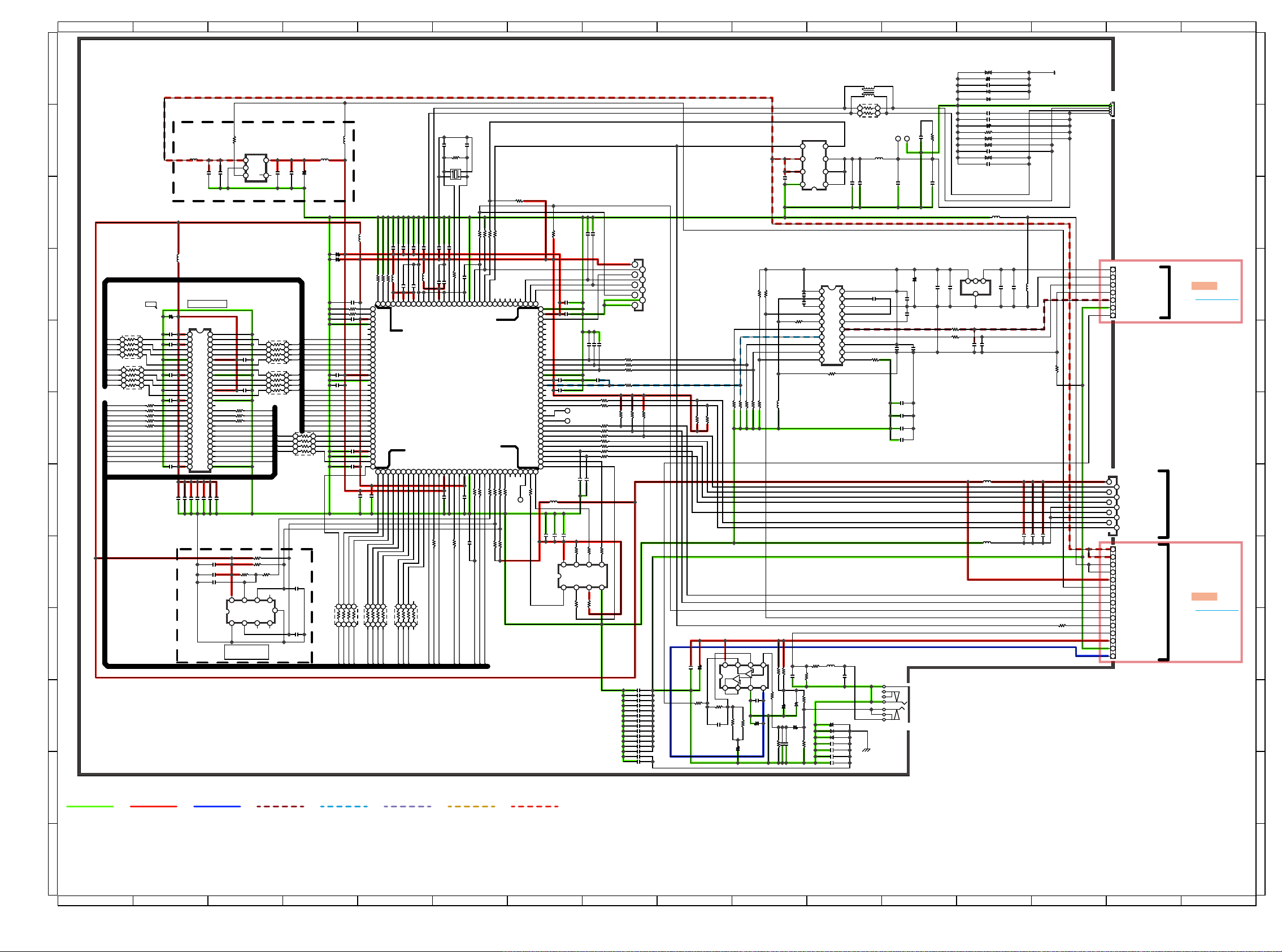
1
2 3 4 5 6 7 8 9 10 11 12 13 14 15 16
A
B
C
D
E
F
G
H
J
K
USB / BT PART ( SETUP MIC )
D5V
OPTION
L9026
CB05YTYH221
C9110
USB3V3
L9018
CB05YTYH221
+3.3V
C9014
10/16V
RN901
C9045
33X4
4 3 2 1
RN902
0.1uF
8 7 6 5
8 7 6 5
4 3 2 1
33X4
0.1uF
C9048
R9053
R9055
R9056
R9057
C9049
0.1uF
D0
D1
D2
D3
D4
D5
D6
D7
LDQM
WEN
CASN
RASN
SDCSN
AD13
AD14
10
AD
AD0
AD1
AD2
AD3
SDRAM 64Mbit
IC902
W9864G6JH-6
545352515049484746454443424140393837363534333231302928
VDD
DQ0
C9046
VDDQ
0.1uF
DQ1
DQ2
VSSQ
DQ3
DQ4
C9047
VDDQ
0.1uF
DQ5
DQ6
VSSQ
DQ7
470
470
470
470
470
VDD
LDQM
/WE
/CAS
/RAS
/CS
BA0/A13
BA1/A14
A10/AP
A0
A1
A2
A3
VDD
27 26 25 24 23 22 21 20 19 18 17 16 15 14 13 12 11 10 9 8 7 6 5 4 3 2 1
0.01uF
0.01uF
0.01uF
0.01uF
1000P
1000P
C9065
C9066
C9067
C9068
C9082
C9083
C9094
C9062
C9063
10uF/6.3V
VSS
DQ15
VSSQ
DQ14
DQ13
VDDQ
DQ12
DQ11
VSSQ
DQ10
DQ9
VDDQ
DQ8
VSS
NC
UDQM
CLK
CKE
AD12
A11
A9
A8
A7
A6
A5
A4
VSS
C9109
1000P
C9084
OPEN
OPEN
OPEN
IC903
OPEN
0.1uF
R9059
R9038
R9058
Apple Auth.
R9089
VCC
GND
1 2 3 4
IC909 USE : L9017 OPEN
IC909 NOT USE : R9089 OPEN
100
IC909
BU12TD3WG-TR
51
VOUTVIN
2
GND
4
3
OC
EN
C9112
10uF/6.3V
RN903
33X
4
C9051
4 3 2 1
0.1uF
RN904
33X4
C9050
4 3 2 1
0.1uF
470R9054
UDQM
220
SDCLK
470
CKE
AD12
AD11
AD0
AD9
AD1
AD8
AD2
AD7
AD6
AD3
AD5
AD4
OPEN
R9029
OPEN
R9030
R9031
R9070
OPEN
OPEN
5678
NC
SCL
RST
9
SDA
NC
NC
2.0c
L9017
OPEN
L9027
CB05YTYH221
0.1uF
10/16V
C9113
C9111
R9081
R9082
D0
D8
D15
D1
D14
D9
D13
D2
D12
8 7 6 5
D10
D3
D11
D10
D9
D11
D8
8 7 6 5
D4
D12
D5
D13
D6
D14
D7
D15
8 7 6 5
RN905
33X4
C9071
OPEN
C9070
OPEN
C9012
47/6.3V
C9011
220/6.3V
C9097
C9040
C9072
4 3 2 1
USB1V2
L9010
C9081
1000P
10K
10K
0.1uF
0.1uF
1000P
C9099
0.1uF
C9073
1000P
4321
33X4
8765
RN906
AD4
AD5
AD6
AD7
C9074
CP_SDA
CP_SCL
CB05YTYH221
1000P
33X4
RN907
C9075
4 3 2 1
8 7 6 5
AD9
AD8
32 31 30 29 28 27 26 25 24 23 22 21 20 19 18 17 16 15 14 13 12 11 10 9 8 7 6 5 4 3 2 1
10K
1000P
R9083
128
ADIN1
ADIN0
AVDD33
AVSS33
NC
NC
D0
D8
D1
D9
D2
D10
D3
VDD12
VSS12
NC
D11
D4
D12
D5
D13
D6
D14
D7
D15
ADO0
ADO1
ADO2
VDD33
VSS33
ADO3
ADO4
33
AD10
C9096
C9080
0.1uF
L9015
10K
10K
C9015
CB05YTYH221
R9084
R9085
127
126
125
124
_VSS12
PLL2
PLL2_VDD12
126.ADIN4
128.ADIN2
127.ADIN3
33.AD5
34.AD6
AD8
AD9
4 3 2 1
33X4
8 7 6 5
RN908
AD11
AD12
AD13
10uF/6.3V
1000P
C9018
C9042
10uF/6.3V
0.1uF
122
123
121
PLL2_VSS12
PLL2_VDD12
PLL2_VDD12
35.AD7
AD10
AD11
AD12
3837363534
AD14
C9087
10uF/6.3V
C9079
C9017
0.1uF
C9041
L9014
9044
C
10uF/6.3V
0.1uF
C9016
CB05YTYH221
118
116
120
119
117
115
IVSS33
USB_D-
USB_D+
USB_VSS33
USB_VDD33
PLL2_VSS12
IC901
BX8804
USB DECORDER
AD13
VDD12
BA14
LDQM
UDQM
SDCSN
4645444342
414039
0.1uF
C9043
220
R9034
LDQM
UDQM
SDCSN
R9033
X9001
12MHz
114
VDD33
VSS12
47
L9022
OPEN
21
43
RN909
OPEN
1SS355T
1SS355T
OPEN
0.1uF
1000pF
OPEN
C1418
0.1uF
1uF
C9033
C9059
CPVDD
12345678910
CAPP
CPGND
CAPM
VNEG
OUTL
OUTR
AVDD
AGND
DEMP
0.1uF
MIC
MICDET
JACK IN : SW OPEN
CHASSIS
(METAL
0 X 2
L9011
CB05YTYH221
C9035
2.2uF 6.3V
R9028
10K
PLATE)
C9054
JK105
CJJ2D029Z
1
7
6
2
3
5
4
T9002
T9001
0.1uF
C9100
C9055
100
0.1uF
C9060
R9073
0.1uF
C9028
OPEN
C9013
C9056
0.1uF
C9036
2.2uF 6.3V
0.1uF
C9020
10uF/6.3V
C9121
0.1uF
C9120
0.1uF
C9122
0.1uF
C9128
0.1uF
MIC
IC905
15P
CVIBD82065FVJ-E2
15P
C9086
1M
1uF
C9034
R9088
10K
100K
1K
100
OPEN
1000P
560
R9066
113
XO
48
220
R9035
CKE
R9086
R9087
R9071
R9032
0.01uF
C9064
112
111
110
109
108
107
106
105
104
103
102
XI
TEST
IVS33
RESET
NTRST
CASN
VSS33
SDCLK
CKE
RASN
VDD33
51
50
49
220
220
R9036
R9037
0.1uF
C9061
10P
C9069
RASN
SDCLK
CASN
101
NC
NC
NC
NC
NC
BD82065_OC
BD82065_EN
98.TMS
97.TDO
99.TMS
100.TCK
61.NC
63.FLASH_CS
64.FLASH_CLK
62.NC
WEN
GND
NC
NC
CP_SDA
CP_RESET
CP_SCL
605958
57
56
55
545352
0
OPEN
OPEN
OPEN
R9074
R9078
R9041
R9042
OPEN
OPEN
R9039
R9040
WEN
99
100
VSS12
VDD12
I2S_LRCK
I2S_BCK
I2S_MCLK
VSS33
VDD33
I2S_DATA
BT I2C_SCL
BT_I2C_SDA
USB_TX
USB_RX
BT_RST
BT_RTS
BT_CTS
BT_RX
BT_TX
FLASH_DI
FLASH_DO
61
T62
10K
R9023
98
97
9695949392919089888786858483828180797877767574737271706968676665
TDI
NC
NC
NC
NC
NC
NC
NC
NC
NC
NC
NC
NC
646362
470
L9013
CB05YTYH221
R9050
C9023
10uF/6.3V
IC904
SERIAL FLASH
C9078
1000P
C9098
0.1uF
C9039
0.1uF
C9077
1000P
T75
T74
0.1uF
1000P
C9095
C9076
8 7 6 5
VCC
/CS
MX25L1606EM2I-12G
220P
220P
C9088
C9089
for DEBUG
CN913
1
1.VCC
2
2.NTRST
3
3.TDI
4
4.TCK
5
5.TMS
6
6.TDO
7
7.RESET
8
8.DGND
9
9.DGND
33P
33P
33P
C9091
C9092
C9090
C9093
R9048
R9049
R9052
R9051
R9072
R9047
R9046
R9075
R9076
OPEN
OPEN
C9038
C9057
47
10K
R904547R9077
R9069
SCLK
/HOLD
SO
/WP
47
10K
R9043
R9068
100
R9018
100
R9019
100
R9020
33P
47
R9010
47
47
10K
10K
10K
R9067
R9044
R9022
470
470
1K
47
47
0
0
SI
GND
4321
10K
10K
R9079
R9080
10K
OPEN
C9052
0.1uF
C9053
0.1uF
R9026
R9025
10K
OPEN
OPEN
OPEN
OPEN
OPEN
L9029
R9062
R9063
R9064
R9065
R9024
CVINJM8080G
C9114
C9115
C9116
C9117
C9118
C9119
C9123
C9127
C9126
C9129
C9130
C9131
C9132
C9124
C9125
OPEN
OPEN
10/16V
V+
0.1uF
8 7 6 5
V+
B OUTPUT
R1408
C1408
A
IC101
- +
A OUTPUT
A-INPUT
O
C1406
0.1uF
56K
4K7
820
27P
R1407
R1027
C1407
100/16V
C1417
R1409
C1411
100
0.1uF
0.1uF
0.1uF
0.1uF
0.1uF
0.1uF
0.1uF
0.1uF
0.1uF
0.1uF
0.1uF
0.1uF
0.1uF
-+
B
C1410
10/16V
2.2K
+-O
OPEN
B-INPUT
B+INPUT
C1401
V-
A+INPUT
R1411
R1412
4321
V-
+-
100
R1406
10/16V
C1405
C1402
1/50V
100K
OPEN
100PF
C1403
R1404
C1404
R9017
10K
MIC_SIGNAL
A
MIC_DET
+12V
-12V
0.1uF
D1401
GND
5.1V(0.5W)
EN /OC
IN
IN
1 2 3 4
GND
R1402
100K
R1403
OUT
OUT
OUT
CVIPCM5100PWR
DVDD
DGND
LDOO
XSMT
FMT
LRCK
DIN
BCK
SCK
FLT
R1401
56K
100K
2.2K
R1405
C1412
D1404
D1405
C1413
C1414
C1415
C1416
5678
IC906
11 12 15 16 17 18 19 201413
R9090
L1401
C
0
B03YTYH600
R9060
R9061
D9014
CDS3C05HDMI1
OPEN
C9107
C9029
0.1uF
1SS355T
D9010
D9011
1SS355T
C9037
OPEN
C9030
0.1uF
C9010
220/6.3V
2.2K
R9012
D9015
CDS3C05HDMI1
D9013
CDS3C05HDMI1
C9032
OPEN
D9012
CDS3C05HDMI1
C9031
OPEN
L9023
CB03YTYH600
IC907
NJM2845DL133
3 1
IN
OUT
0.1uF
C9021
10uF/6.3V
470
470
C9026
2200P
0.1uF
C9022
C9103
GND
2
C9027
2200P
10uF/6.3V
CHASSIS
METAL PLATE
L9025
OPEN
CJJ9X010Z
JK91
4321
BN914
4.DGND
3.USBD+
2.USBD-
1.VBUS
1.+5VA
2.DA_GND
3.USB/BT_R
4.DA_GND
5.USB/BT_L
6.AGND
7 6 5 4 3 2 1
7.MIC_SIG
BN914
TO CN752
TO DIGITAL B'D
DIGITAL POWER PART
0
A
B
C
D
E
R9091
F
BN912
CN911
1
3
5
7
9
1.VDD
2
2.RESET
3.RTS
4
4.CTS
5.TXD
6
6.BT_GND
7.RXD
810
8.BT_GND
9.I2C_SCL
10.I2C_SDA
1.D5V
2.D5V
3.DGND
4.DGND
5.USB3V3
6.USB_POWER1
/USB1V2
7.USB_TX
8.USB_RX
9.BX_RST
10.USB_DAC_MUTE
11.USB_EN
12.MIC_DET
13.+12V
14.AGND
15.-12V
15 14 13 12 11 10 9 8 7 6 5 4 3 2 1
TO BT MODULE
MCU PART
TO DIGITAL B'D
G
H
BN912
TO CN713
J
L9019
CB05YTYH221
L9024
CB03YTYH600
10uF/6.3V
C9019
0.1uF
1000P
C9058
C9085
0
R9092
K
L
M
GND LINE
1
POWER+ LINE
2 3 4 5 6 7 8 9 10 11 12 13 14 15 16
POWER- LINE
L
ANALOG AUDIO DIGITAL AUDIO TMDS SIGNAL ANALOG VIDEO STBY POWER
M
SCHEMATIC DIAGRAMS (7/12)
USB BT
71
Page 72
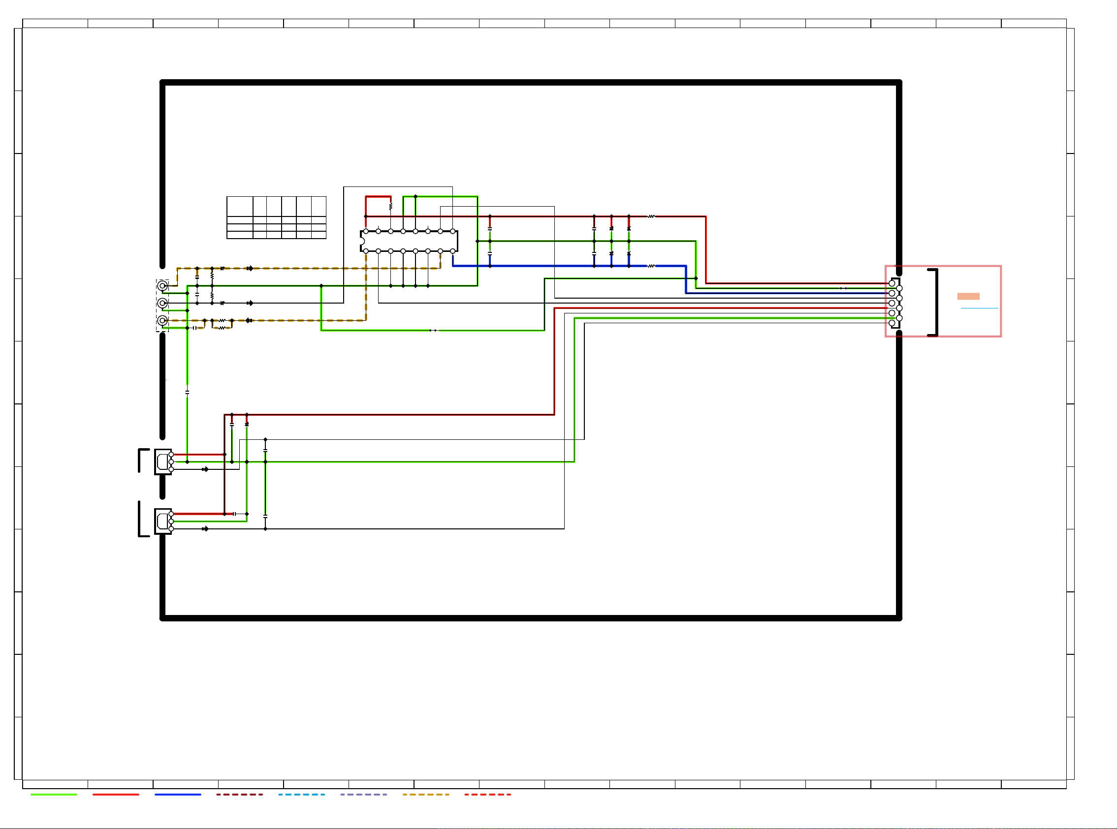
1 2 3 4 5 6 7 8 9 10 11 12 13 14 15 16
A
B
C
D
CBL/SAT IN
E
DVD IN
MONITOR OUT
COMPOSITE IN/OUT
VIDEO/OPTICAL PART
NLM2595 S/W TABLE(SW2,5 CONTROL)
CJJ4S010Z
JK781
C7801
SW1
FUNC.IN
MUTE
DVD L
10/50V
C7805
75(1%)
R7804
OPEN
C7803
OPEN
75(1%)
R7803
C7802
22pF
1.8K
R7801
82(1%)
R7802
10/50V
C7804
SW2
(14)
FIX FIX FIX
H
H H
SW4
SW3
(10)
L
X (L)
X
LH
X
SW5
(6)
(4)
(2)
L
L
H
(L)
LSAT/CBL
H
(L)
VCC
IC781
1 2 3 4 5 6 7 8
NJM2595MTE1
V01
A
B
C
10K
R7806
R7807
VO2
SW1
SW5
VIN5
VO3
SW2
VIN1
GND
VIN4
SW3
VIN2
910111213141516
VSS
SW4
VIN3
J7805
OPEN
C7806
0.1uF
C7807
0.1uF
OPEN
C7808
C7810
10/50V
OPEN
C7809
C7811
10/50V
270(1W)
5.1V
D7801
5.1V
D7802
R7808
270(1W)
CN781
1.+12V
J7806 OPEN
1
3
5
7
9
2.VGND
2
3.-12V
4.CVBS_SW2
4
5.CVBS_SW5
6.+5VD
6
7.OPT1_IN
8.DGND
8
9.OPT2_IN
CN781
TO CN741
DSP PART
TO DIGITAL B'D
D
E
F
0.1uF
C7714
0.1uF
C7813
C7812
G
JK782
CJSJSR1124
RX
VCC
GND
1 2 3
OUT
100/50V
OPEN
C7814
F
G
CBL/SAT
H
OPTICAL RX 1/2
J
K
TV
JK783
CJSJSR1124
OPT1 OPT2
H
C7715
VCC
RX
GND
1 2 3
OUT
0.1uF
OPEN
C7815
J
K
L
M
GND LINE
L
M
SCHEMATIC DIAGRAMS (8/12)
VIDEO OPTICAL
1
2 3 4 5 6 7 8 9 10 11 12 13 14 15 16
POWER+ LINE
POWER- LINE
ANALOG AUDIO DIGITAL AUDIO TMDS SIGNAL ANALOG VIDEO STBY POWER
72
Page 73

1
2 3 4 5 6 7 8 9 10 11 12 13 14 15 16
A
A
MAIN PART
PTC Thermistors
D5101
R5103
LEFT FRONT-CH
R5101
C5101
10UF/100V
100K
B
FL_IN
10K
R5102
680
470P/100V
FL
Q5101
KSA992FTA
18K
R5104
R5107
220
C5102
R5105 1.2K
R5106
1.2K(1W)
C
R5203
LEFT SURROUND-CH
SL_IN
D
E
CEN_IN
C5201
10UF/100V
100K
R5201
CENTER-CH
C5301
10UF/100V
100K
R5301
CEN
10K
R5202
680
470P/100V
SL
R5302
680
470P/100V
Q5201
KSA992FTA
18K
R5204
R5207
220
C5202
R5205 1.2K
R5206
1.2K(1W)
R5303
10K
Q5301
KSA992FTA
18K
R5304
R5307
220
R5305 1.2K
C5302
R5306
1.2K(1W)
F
R5403
FR
R5402
680
R5502
680
DGND
10K
Q5401
KSA992FTA
18K
R5404
470P/100V
)
R5407
220
C5402
R5405 1.2K
R5406
1.2K(1W
R5503
10K
Q5501
KSA992FTA
18K
R5504
470P/100V
R5507
220
R5505 1.2K
C5502
R5506
1.2K(1W)
RIGHT SURROUND-CH
C5401
SR_IN
10UF/100V
G
H
R5401
FR_IN
R5501
SR
100K
RIGHT FRONT-CH
C5501
10UF/100V
100K
J
C5723
10UF/50V
MUTE_+B
BN501
K
BN501
13121110987654321
TO CN772
1.FL
3.SL
5.CEN
7.SR
9.FR
12.MUTE_+B
2.AGND
4.AGND
6.AGND
8.AGND
TO DIGITAL B'D
INPUT/VOLUME PART
13.DGND
10.+12V
11.RLY_GND
OPEN
OPEN
D5201
OPEN
OPEN
D5301
OPEN
J5301
OPEN
D5401
OPEN
OPEN
D5501
OPEN
J5101
J5201
J5401
J5501
OPEN
C5105
C5205
C5305
C5405
C5505
R5108 470K
C5106 33P
R5109 33K
220/50V
R5208 470K
C5206 33P
R5209 33K
220/50V
R5308 470K
C5306 33P
R5309 33K
220/50V
R5408 470K
C5406 33P
R5409 33K
220/50V
R5508 470K
C5506 33P
R5509 33K
220/50V
C5103
82P
Q5102
KSA992FTA
C5104
2200P(M)
5203
C
82P
Q5202
KSA992FTA
C5204
2200P(M)
C5303
82P
Q5302
KSA992FTA
C5304
2200P(M)
C5403
82P
Q5402
KSA992FTA
C5404
2200P(M)
C5503
82P
Q5502
KSA992FTA
C5504
2200P(M)
TUNER MODULE
TU500
1 2 3 4 5 6 7 8
Q5103
KSC1845FTA
R5110
47(1W)
Q5203
KSC1845FTA
R5210
47(1W)
Q5303
KSC1845FTA
R5310
47(1W)
Q5403
KSC1845FTA
R5410
47(1W)
Q5503
KSC1845FTA
R5510
47(1W)
Q5104
KTC3114A
2.7K
R5113
560
R5112 OPENR5212 OPENR5312 OPENR5412 OPENR5512 OPEN
R5111 OPEN
R5114
PRE_-B
Q5204
KTC3114A
2.7K
R5213
560
R5211 OPEN
R5214
Q5304
KTC3114A
2.7K
R5313
560
R5311 OPEN
R5314
Q5404
KTC3114A
2.7K
R5413
560
R5411 OPEN
R5414
PRE_-B PRE_-BPRE_-B
Q5504
KTC3114A
2.7K
R5513
560
R5511 OPEN
R5514
+12V
DGND DGND
AGND AGND
PRE_-B
MUTE_+B
CHASSIS
2.0mm 13PIN WIRE
L
*TUNER MODULE OPTION
E1
AVR-X510BT
AVR-X510BT E1C
CNVYST990-A9U1AVR-S500BT E3
CNVYST990-D8E1
CNVYST990-A2J1
987654321
BN508
BN508
CJP09GI281Z
TO TU771
VR510
VR520
VR530
VR540
VR550
1K
1K
1K
1K
1K
R5115
5.6K(1W)
C5107
R5215
5.6K(1W)
C5207
R5315
5.6K(1W)
C5307
R5415
5.6K(1W)
C5407
R5515
5.6K(1W)
C5507
D5704 1SS133
R5116
5.6K(1W)
R5117
4.7(1W)
D5102
OPEN
C5108
D5103
100/63V
10UF/100V
OPEN
D5104
OPEN
D5105
OPEN
4.7(
R5216
5.6K(1W)
4.7(1W)
D5202
OPEN
C5208
D5203
100/63V
10UF/100V
OPEN
D5204
OPEN
D5205
OPEN
4.7(1W)
R5316
5.6K(1W)
4.7(1W)
D5302
OPEN
C5308
D5303
100/63V
10UF/100V
OPEN
D5304
OPEN
D5305
OPEN
4.7(1W)
R5416
5.6K(1W)
4.7(1W)
D5402
OPEN
C5408
D5403
100/63V
10UF/100V
OPEN
D5404
OPEN
D5405
OPEN
4.7(1W)
R5516
5.6K(1W)
4.7(1W)
D5502
OPEN
C5508
D5503
100/63V
10UF/100V
OPEN
D5504
OPEN
D5505
OPEN
4.7(1W)
C5717
10UF/50V
D5703 6.8V
R5714 OPEN
R5715
2.2K(1W)
R5718
OPEN
OPT.
R5118
R5217
R5218
R5317
R5318
R5417
R5418
R5517
R5518
Q5105
2SD2390
CN510
CJP02GA01ZY
0.47(2W)
0.47(2W)
R5121
R5119
R5120
1W)
R5219
R5220
R5319
R5320
R5419
R5420
R5519
R5520
R5716
2.2K(1W)
R5719
OPEN
21
R5122
0.47(2W)
0.47(2W)
Q5106
2SB1560
Q5205
2SD2390
CN520
CJP02GA01ZY
0.47(2W)
0.47(2W)
R5221
21
R5222
0.47(2W)
0.47(2W)
Q5206
2SB1560
Q5305
2SD2390
CN530
CJP02GA01ZY
0.47(2W)
0.47(2W)
R5321
21
R5322
0.47(2W)
0.47(2W)
Q5306
2SB1560
Q5405
2SD2390
CN540
CJP02GA01ZY
0.47(2W)
0.47(2W)
R5421
21
R5422
0.47(2W)
0.47(2W)
Q5406
2SB1560
Q5505
2SD2390
CN550
CJP02GA01ZY
0.47(2W)
0.47(2W)
R5521
21
5522
R
0.47(2W)
0.47(2W)
Q5506
2SB1560
R5717
2.2K(1W)
R5720
OPEN
R5126
PRF18BE471QB5RB
Q5107
MMBT5401
0.1uF
R5123
470K
D5106
R5124
1SS133
R5125 10K
PTC Thermistors
R5226
PRF18BE471QB5RB
R5223
470K
R5224
D5206
1SS133
R5225 10K
PTC Thermistors
R5326
PRF18BE471QB5RB
R5323
470K
D5306
R5324
1SS133
R5325 10K
PTC Thermistors
R5426
PRF18BE471QB5RB
R5423
470K
D5406
R5424
1SS133
R5425 10K
PTC Thermistors
R5526
PRF18BE471QB5RB
R5523
470K
D5506
R5524
1SS133
R5525 10K
AGND
-B
AGNDAGND
PRE_-B
+B +B
DC_FRONT
Q5703
2SC3052
C5109
R512
9 15K
Q5108
MMBT5551
270K
R5127
5.6K
Q5208
MMBT5551
270K
R5227
5.6K
Q5308
MMBT5551
270K
R5327
5.6K
Q5408
MMBT5551
270K
R5427
5.6K
Q5508
MMBT5551
270K
R5527
5.6K
Q5704
ISA1530AC1
R5130 22K
R5131 22K
L5101 0.5UH
R5128
OPEN
R5132 10(1W)
Q5207
MMBT5401
0.1uF
C5209
R5229 15K
R5230 22K
R5231 22K
L5201 0.5UH
R5228
OPEN
R5232 10(1W)
Q5307
MMBT5401
0.1uF
C5309
R5329 15K
R5330 22K
R5331 22K
L5301 0.5UH
R5328
OPEN
R5332 10(1W)
Q5407
MMBT5401
0.1uF
C5409
R5429 15K
R5430 22K
R5431 22K
L5401 0.5UH
R5428
OPEN
R5432 10(1W)
Q5507
MMBT5401
0.1uF
C5509
R5529 15K
R5530 22K
R5531 22K
L5501 0.5UH
R5528
OPEN
R5532 10(1W)
Q5705
0.1uF
100K
R5705
C5710
2SC3052
DC PROTECTION
R5728
OPEN
C5711
0.01uF
C5701
R5701 10K
Q5701
MMBT5401
22K
R5702
FL_OUT
THEMALDET_A
AGNDAGNDAGND
CEN_OUT
FR_OUT
SR_OUT
SL_OUT
SL_OUT
UT
CEN_OUT
SR_O
DC_SURROUND
THEMALDET_ATHEMALDET_A
ASOASOASO ASO
DC_FRONT DC_FRONT DC_FRONT
AGND
DC_SURROUND DC_SURROUND
THEMALDET_A
DC_FRONT
THEMALDET_B
-B -B -B -B
FR_OUT
-B
+12V+12V+12V
RLY_GNDRLY_GNDRLY_GNDRLY_GND
DGND
AGND
PRE_-B
DC_SURROUND
Q5706
2SC3052
10K
R5706
470/6V3
+B +B+B+B
ASO_DET
ASO_DET ASO_DET ASO_DET
C5716 47/16V
Q5707
ISA1530AC1
FR_OUT
FR_OUT
SR_OUT
FR_OUT
R5711 1.2K
R5712 2.2K
R5713 2.2K
Q5708
0.1uF
100K
C5712
R5707
2SC3052
AGND
THERMALDET_A
THERMALDET_B
ASO_DET
DC_PROT
C5713
FL_OUT
CEN_OUT
FR_OUT
SL_OUT
SR_OUT
H/P_RLY
MCU_CTL
FRONT_RLY
C/S_RLY
C/S_RLY
R5814 OPEN
R5815 OPEND5811 OPEN
LEVEL DET.
D5810 OPEN
+B
D5807 OPEN
C5806 OPEN
C5807 OPEN
R5810
R5811 OPEN
DGND
-B
AMPSIG_DET
15K
R5708
470/6V3
+12V
Q5601
RT1N237C
RLY_GND
C5718 0.047u R5721
FL_OUT
Q5602
RT1N237C
FR_OUT
C5719 0.047u R5722
C5720 0.047u R5723
SL_OUT
Q5603
RT1N237C
SR_OUT
C5721 0.047u R5724
C5722 0.047u R5725
CEN_OUT
Q5604
RT1N237C
R5812 OPEN
R5816 OPEN
R5813 OPEN
D5812 OPEN
D5809 OPEN
D5808 OPEN
OPEN
C5708
100/100V
Q5702
KSA992FTA
+12V
RLY_GND
PRE_-B
981-21-12DSRY562
RY563
981-21-12DS
RY564
981-21-12DS
R5704
100(1W)
PRE_-B
BN502
BC3-12H
RY560
D5601
1SS133
D5602
1SS133
D5603
1SS133
D5604
1SS133
J5602
R5703
33(1W)
HI-B_RLY
H/P_RLY
C/S_RLY
FRONT_RLY
AMPSIG_DET
TO CN712
3.FRONT_RLY
4.C/S_RLY
2.H/P_RLY
1.HI-B_RLY
5.AMPSIG_DET
817
10(2W)
RY562
615 4
10(2W)
10(2W)
RY563
615 4
10(2W)
10(2W)
615 4
RY564
J5604
ASO_DET
DC_PROT
6.ASO_DET
7.DC_PROT
2
THERMALDET_A
2 3
2 3
2 3
8.THERMALDET_A
43
56
C5704
6800uF/63V
R5709
R5710
AGND
RLY_GND
THERMALDET_B
BN502
987654321
9.THERMALDET_B
R5726 470(2W)
R5727 470(2W)
H/P_FR
H/P_FL
BN505
3 2 1
1.HP_RCH
2.AGND
3.HP_LCH
BN505
TO CN104
TO FRONT B'D
B
2.0mm 3PIN WIRE
C
1500P
C5608
1500P
C5613
OPEN
OPEN
D5701
HVDGBJ606
D5806
1SS133
-12DS
C5605
0.018u
C5606
0.018u
C5609
0.018u
C5610
0.018u
C5611
0.018u
RY586
C5616
OPEN
C5617
OPEN
1500P
C5618
OPEN
C5619
OPEN
C5620
OPEN
1500P
1500P
C5614
1
2
3
4
JK503
CJJ5P038Z
1
2
3
4
5
6
JK504
CJJ5R021Z
D
SL-CHC-CH SR-CH FR-CH FL-CH
SL-CHC-CH SR-CH
E
F
BK501
M3 BRACKET
CMD1A569-V1
2
4
1
3
C5702 0.1u/250VC5703 0.1u/250V
C5714 OPEN
C5715 OPEN
RECHECK
F5801
T5AH 250V
7
1534862
T5AH 250V
RECHECK
J5804
OPEN
J5805
OPEN
F5802
123456
7
CN503
CJP07GA90ZY
AC_L
N.C
AC_H
CEN
AC_H
N.C
AC_L
FROM MAIN TRANS
3.96mm 7PIN WAFER
G
H
J
K
FL_OUT
FR_OUT
C5607
SL_OUT
SR_OUT
CEN_
OUT
C5612
J5601
OPEN
OPEN
0.1/50V
C5707
ET501
CHASSIS
Q5806
RT1N237C
C5706
6800uF/63V
C5615
942H-2C
TO DIGITAL B'D
MCU PART
2.0mm 9PIN WIRE
PTC Thermistors
THERMALDET_A
THERMALDET_B
FL-CH, SL-CH, CEN_CH
FR-CH, SR-CH
L
M
GND LINE
1
1.CH_GND
7.VCC
6.SCLK
5.SDIO
4./CE
3./RST
2.INT
SCHEMATIC DIAGRAMS (9/12)
POWER+ LINE
POWER- LINE
9.L-OUT
8.R-OUT
TO DIGITAL B'D
9PIN B'D TO B'D
ANALOG AUDIO DIGITAL AUDIO TMDS SIGNAL ANALOG VIDEO STBY POWER
MAIN
2 3 4 5 6 7 8 9 10 11 12 13 14 15 16
73
M
Page 74

1 2 3 4 5 6 7 8 9 10 11 12 13 14 15 16
BN1281
23.CPU_POWER
2325
KEY_3KEY_2KEY_1
R1083R1082R1081
SOUND+
SOUND+
PRESET+
22.FL_DATA
Z2 SEL
21.FL_CLK
TO CN711
FL_CE
18.RC_IN
20.
19.FL_RST
1921
2022
R1084 R1085
4R1082R1081R1080R1079R1078R1077R1076
KEY_3KEY_2KEY_1
DIMMER
TUNE-
DIMMER
CN104
2.ISEL_B
9.B/P_IRIN_DE
8.AGND
13.KEY_3
14.KEY_2
16.RED_LED
17.W/G_LED
15.KEY_1
12.VSEL_B
11.VSEL_A
10.H/P_DET
1517
16318
1.ISEL_A
3.MIC_DET
5.+12V
6.-12V
7.MIC_SIGNAL
4.POWER_KEY
AVR-X1100W E3 ONLY
1
24567891011121314
R1069
390
390
R1418
R1419
1K
option
47K
R1420
RT1P141C
R1022
1K
Q1007
RC101
VOUT GND Vcc
1 2 3
R1024
OPEN
10
100P
(37.9kHz)
AVR-S500BT/X510BT
Q1007 OPEN
R1022 OPEN
R1023 OPEN
R1069 1K
AVR-S700W/X1100W
Q1007 RT1P141C
R1022 1K
R1023 47K
R1069 OPEN
C1038
47/16V
(SMALL)
+3V3
D_GND
VOL-
VOL+
R1061 10K
R1060 10K
R1059
R1058
OPEN
D1015
1K
1K
A B
VR101
0.01uF
0.01uF
C1076
C1077
CSR2A055Z
C
VOLUME
24CLICK
0.1uF
OPEN
OPEN
OPEN
C1074
C1075
C1073
D1016
ENCODER
(SMALL)
LUG11
CHASSIS
WIRE
OPEN
OPEN
LD101
OPEN
SIR341ST3FT0
C1430
R1421
D1408
R1053
C1039
47K
R1023
A
B
C
CUP12619Z-1
BN12A
1. AGND
2. MIC_SIGNAL
3. -12V
4. +12V
5. MIC_DET
5.1V
47K
OPEN
D1403
5.1V
C1409
R1410
D1402
OPEN
C1082
1K1.5K1K1.5K1K1.5K2.7K3.3K5.6K
R1085R108
5 4 3 2 1
CVINJM8080G
1/50V
V+
8 7 6 5
V+
C1417
0.1uF
(SMALL)
C1411
IC101
R1409
A OUTPUT
O
R1408
100
18K
C1408
82P
L1403
CB03YTYH600
1. AGND
2.0mm 5PIN WIRE
2.0mm 5PIN WIRE
BN12B
2. MIC_SIGNAL
3. -12V
4. +12V
5. MIC_DET
5 4 3 2 1
+-O
-+
B-INPUT
B
B OUTPUT
A
- +
V-
A+INPUT
A-INPUT
4321
V-
+-
0.047uF
C1406
4K7
820
C1410
1/50V
(SMALL)
R1027
R1407
C1407
100/16V
(SMALL)
CUP12619Z-2
2.2K
OPEN
B+INPUT
0.1uF
C1401
R1412
R1411
100
R1406
10/50V
C1405
(SMALL)
C1402
1/50V
(SMALL)
100K
100P
R1404
C1403
C1404 OPEN
R1054
OPEN
L1401
R1401
CB03YTYH600
100
100K
R1402
2.2K
5.1V
D1401
R1405
100K
R1403
D1404
D1405
C1415
C1413
C1414
C1416
C1412
OPEN
1SS355
1SS355
OPEN
0.1uF
1000P
OPEN
MICDET
JK105
CJJ2D029Z
1
7
6
L1402
CB03YTYH600
2
MIC
3
5
4
MIC
JACK IN : SW OPEN
D1008
CVDCDS3C05HDMI1
OPEN
C1078
C1053
BAND
Q/S_1
BAND
Q/S_1
DIMMER
Q/S_3
DIMMER
Q/S_3
Q/S_3
Q/S_3
0.1uF
1SS355T
D1020
D1019
AVR-S500BT/X500BT
10K
ONLY
R1046
C1081
0.1uF
-
3.H/P_DET
2.DGND
1.DGND
3 2 1
CN103
2.0mm 3PIN WAFER
54321
BN104
5.DGND
4.DGND
3.USBD-
2.USBD+
1.VBUS
L1404
CB03YTYH600
1SS355T
C1051
OPEN
C1050
0.1uF
C1052
220/10V
2.2K
R1040
D1011
CVDCDS3C05HDMI1
D1010
CVDCDS3C05HDMI1
C1049
OPEN
D1009
CVDCDS3C05HDMI1
OPEN
C1048
CUP12619Z-5
(SMALL)
0
L1005
L1008
CHASSIS
METAL PLATE
CJJ9X010Z
JK101
4.DGND
3.DATA+
2 3 4
2.DATA-
1
1.VBUS
0
L1003
L1004
L1009
OPEN
OPEN
CB08YTYH600
iPOD/USB
D
E
F
G
H
AVR-S500BT/X510BT/S700W/X1100W FRONT PART
A
F1001
T 100mA L 250V
B
7. FL_AC
6. NC
5. FL_AC
4. NC
3. GND
C
2. NC
1. VDISP
1 2 3 4 5 6 7
CN102
CJP07GB03ZY
D1001
1N4007ST
1080
C
OPEN
C1079
OPEN
OPEN(AXIAL)
C1001
OPEN(AXIAL)
R1001
1.8(AXAL)
R1002
OPEN
R1003
R1004
1.8(AXAL)
220/63V
OPEN
OPEN
C1005
R1029
R1417
C1002
Q1001
KTC1027YT
10K
OPEN
R1062
R1007
13V
D1005
1/50V
C1006
R1006
0.1uF/100V
R1005
24V
D1004
C1003
0
22
220
10/50V
R1009
(SMALL)
D1003
6.8V
220
220
R1008
FL101
CFL18BT021GINK
F2
NP
VFL
GND
57 53 52 51 50 49 48 47 46 45 44 43 8 7 6 5 1
OPEN
0.047uF
C1423
OPEN
R1030
10(AXIAL)
C1004
100/50V
C1418 OPEN
C1419 OPEN
C1009
C1007
C1420 OPEN
C1421 OPEN
0.1uF/50V
C1008
R1067
10/16V
C1010
(SMALL)
C1011
0.1uF
C1422 OPEN
R1068
Q1002
RT1N141C
DACPCS
TSB
TSA
OSC
VDD
VDDH
RESET
OPEN
C1012
100P
C1013
100P
C1014
10(AXIAL)
100
R1012
39K
0
R1010
R1011 10K
100
100
100
R1013
R1014
R1015
330P
C1015
C1016
1000P
AVR-S500BT/X510BT
Q1002 OPEN
R1011 OPEN
R1068 0
AVR-S700W/X1100W
Q1002 RT1N141C
R1011 10K
R1068 OPEN
NX
Q1003
2SC3052
39K
R1025
+3V3
18G
100
R1018
100K
R1026
R1016
F1
NP
17G
Q18G
Q17G
OPEN
OPEN
0.047uF
C1017
C1018
C1041
100
R1019
Q1004
2SC3052
100K
39K
R1017
Q1005
L1001
CB03YTYH600
ISA1530AC1
BN12B1
CJP27GB286ZN
1K
3.3K
+3V3
R1021
R1020
Q1006
RT1N141C
27.DGND
26.DGND
24.MCU_5V
25.MCU_3V3
27
2426
0.01uF
10/50V
C1019
C1020
D
KEY_1
KEY_2
*OPTION
R1075
OPTION
SW113
R1080
OPTION
SW119
R1085
OPTION
KEY1
*OPTION
KEY2
KEY3
KEY NAME
AVR-S500BT SOUND-
AVR-X510BT
AVR-S700W
AVR-X1100W
AVR-S500BT/AVR-X510BT RESISTOR VALUE
AVR-S500BT 2.7K3.3K5.6K 2.7K3.3K5.6K
AVR-X510BT
AVR-S700W/AVR-X1100W RESISTOR VALUE
OTHER 100150 00100150 0100150180
KEY OPTION
TONE
NIGHT
-
-
GAME
PURE
- -
OPEN OPEN OPEN 1.5K OPEN
R1071 R1073 R1075R1074R1072 R1083
OTHER
STATUS
TUNE+
Z2 ON/OFF
STATUS
ED
8. MCU+5
7. RED_L
SW106 SW107
R1074
OPTION
SW112
R1079
OPTION
SW118
R1084
OPTION
C1088 OPEN
C1089 OPEN
C1090 OPEN
C1091 OPEN
9. POWER_KEY
SW103SW102
E
SW108
W/G_LED
RED_LED
SW114
F
R1071
OPTION
SW109
R1076
OPTION
SW115
R1081
OPTION
SW104
R1072
OPTION
SW110
R1077
OPTION
SW116
R1082
OPTION
SW105
R1073
OPTION
STATUSPRESET+
SW111
R1078
OPTION
SW117
R1083
OPTION
G
C1087 OPEN
C1086 OPEN
C1085 OPEN
2. ISEL_A
3. ISEL_B
1. +3V3
4. DGND
5. DGND
1 2 3 4 5 6 7 8 9
H
BN101_1
2.0mm 9PIN WIRE
KEY_3
R1076
0
1K1.5K
KEY_1 KEY_2 KEY_3
100 100150180220330100150180220330150180220330AVR-S700W
SW102 SW103 SW104 SW105 SW106 SW107 SW108 SW109 SW110 SW111 SW112 SW113 SW114 SW115 SW116 SW117 SW118 SW119
O O O O O O O O O O O O O O O O O
OAVR-S500BT/AVR-S700W
X O O O X X X X X XO O O O O O O
X
RESTORETUNE+ TUNE-
PRESET-
PRESET-
PRESET-
SOUND-
Z2 ON/OFF
PRESET-
Q/S_1
Q/S_1
PRESET+
-
PRESET+
-
PRESET+
MOVIE
-
Z2 SEL
- Q/S_4
R1079 R1080R1077R1072 R1074 R1075 R1078R1073R1071
MODE STATUS
Q/S_2
Q/S_4
MODE
Q/S_2
001K 01K1.5K2.7K
OPENOPEN0OPENOPEN
SW114SW113SW112 SW115 SW116 SW118SW117 SW119SW111SW110SW109SW108SW107SW106SW105SW104SW103SW102
Q/S_4
EQ
Q/S_2
-
- -
-
Q/S_2STATUS
MUSICQ/S_4
- -
-
TO BN505
1.HP_RCH
3.HP_LCH
2.AGND
2.0mm 9PIN WIRE
BN101
1 2 3 4 5 6 7 8 9
R1043
R1044
OPEN
4K7
D1012
R1041
R1042
R1043
R1044
D1002
R1041
R1042
CVDBLBJEGJ204L
C1054
LED OPTION
AVR-X1100W E3 OTHER
WHITE/RED
1K2
1K2
4K7
OPEN
1SS133M OPEN
1K2
1K2
D1012
R G
R1045
OPEN
D1002
1SS133MT
C1055
0.1uF
GREEN/RED
SB-LED
0.1uF
OPEN
1K2
1K2
4K7
1. +3V3
4. DGND
5. DGND
2. ISEL_A
J
CUP12619Z-3
K
12CLICK
FUNCTION
ENCODER
R1413 10K
R1414 10K
R1415
R1416
AB
VR102
0.01uF
0.01uF
C1425
C1426
CSR2A060Z
C
OPEN
OPEN
OPEN
OPEN
(SMALL)
C1428
C1427
D1407
C1429
L
3. ISEL_B
1K
1K
OPEN
D1406
LUG14
OPEN
CHASSIS
8. MCU+5
7.RED_LED
6. W/G_LED 6. W/G_LED
9. POWER_KEY
ON/STANDBY
SW101
Q1008
RT1P141C
Q1009
RT1N141C
Q1011
RT1P141C
Q1012
RT1N141C
ENCODER&POWER
GND LINE
POWER+ LINE
POWER- LINE
ANALOG AUDIO DIGITAL AUDIO TMDS SIGNAL ANALOG VIDEO STBY POWER
CN104
CUP12619Z-4
JK104
CJJ2E026Z
(SILVER)
123
470
R1057
C1071
680P
C1072
680P
L1012
CB03YTYH600
8
237
7. DET
8. DGND
2. HP_LCH
3. HP_RCH
M
2.0mm 3PIN WIRE
3.H/P_DET
2.DGND
1.DGND
123
BN131
L1011
CB03YTYH600
C1424
0.1uF
C1069
N
OPE
CB03YTYH600
1
1. AGND
C1084
L1010
CB03YTYH600
1/50V
0.1uF
C1083
C1068
LUG13
CHASSIS
WIRE
C1067
OPEN
L1013
HEADPHONE
AVR-S700W/X1100W ONLY
J
OPEN
K
C1065
0.1uF
C1066
1/50V
L
M
SCHEMATIC DIAGRAMS (10/12)
FRONT
1
2 3 4 5 6 7 8 9 10 11 12 13 14 15 16
74
Page 75

1
2 3 4 5 6 7 8 9 10 11 12 13 14 15 16
A
B
C
REGULATOR PART
FUSE OPTION
F3002
218Series
OPEN 932Series
F3003 F3004
OPEN
OPENS700W/X1100W
932Series
S500BT/X510BT
F3001
218Series
OPEN
A
B
D3101
OPEN
IC305
CVIKIA7805BPI
OUTIN
321
C3001
C3002
D3108
GND
OPEN
OPEN
OPEN
C3008
OPEN
C3009
470/50V
J3001
OPEN
C
FUSE OPTION
F3004
T 1.25A L 250V
932 TYPE
F3002
D
1.AC_S2
2.NC
E
3.RTN_GND
FROM TRANS
4'.NC
5.AC_S2
5 4 3 2 1
CN302
T 1.25A L 250V
F3001
T 1.25A L 250V
F3003
T 1.25A L 250V
932 TYPE
OPEN
C3004
OPEN
C3003
C3005
0.1uF/100V
D3001 1N4007
D3002 1N4007
D3003 1N4007
D3004 1N4007
C3006
C3010
4700/25V
C3007
C3011
3300/25V
OPEN
J3002
C3024
IC301
CVIKIA7812BPI
OUTIN
321
GND
OPEN
OPEN
HVIKIA7912PI
IC302
D3103
D3104
GND
OUTIN
312
OPEN
C3012
C3014
470/50V
1SS133MT
BN301
V
OPEN
C3013
C3015
470/50
1SS133MT
J3003
OPEN
J3007
1.DA+5V
DA_GND
3.+12V
4.AGND
5.-12V
6.RLY_GND
VGND(RET_GND)
7 6 5 4 3 2 1
BN301
TO CN771
D
E
BN302
BK303BK302
123
1.MCU_3V3
3.DGND
1A569 1A387
2.B/P_IRIN_DE
Bracket
F
No connection
G
F
C3026 OPEN
C3025 OPEN
3
2
JK301
CJJ2D008Z
G
1
1000P
D3200
C3100
1SS355T
BK301
CHASSIS
1A569
Q3001
RT1P141C
3.3K
R3002
1K
OPEN
D3201
R3001
Q3002
2SC3052
2.2K
R3003
100K
R3004
REMOTE IN
AVR-X1100W E3 ONLY
H
J
K
H
J
K
L
GND LINE
M
L
POWER+ LINE
POWER- LINE
ANALOG AUDIO DIGITAL AUDIO TMDS SIGNAL ANALOG VIDEO STBY POWER
M
SCHEMATIC DIAGRAMS (11/12)
REGULATOR
1
2 3 4 5 6 7 8 9 10 11 12 13 14 15 16
75
Page 76

1 2 3 4 5 6 7 8 9 10 11 12 13 14 15 16
A
B
C
D
E
F
G
SMPS PART
BK602
CMD1A188
2 1
CN601
YAW396-NNV
BK601
CMD1A188
CY601 470P 250V
C6001
CN602
YW396-NNB
2 1
TO POWER TRANS
AVR-S700W/X1100W
E3,K T 6.3A L 250V
E2,E1,E1C T 3.15A L 250V
AVR-S500BT/X510BT
E3 T 4A L 250V
E2,E1,
E1C T 2.5A L 250V
E2,E1,E1C T 1.6A L 250V
CY602 470P 250V
3
0.01uF 250V
RY601
HL31-1A
F6002
OPTION
OPTION
E3,JP T 2A L 250V
F6001
142
A
B
D6013
BK603
CMD1A629
RBQ30T65A
1
3
D6011
OPEN
1
3
2
2
.1uF(1608)
4.7uF(1608)
C6015
C6014 0
C6024 0.1uF(1608)
R6026
OPEN(1608)
C6025 OPEN(1608)
1A834
1A834
BK602 BK601
C
D
R6016
56(0.2W)
R6020
R6021
OPEN(1608)
22K-F(1608)
OPEN
OPEN(0.2W)
6.8V
ZD619
E
BN601
D5.2V
D5.2V
DGND
DGND
1 2 3 4 5
MAINPOWER
BN601
TO CN751
OPEN
C6010
6.8K-F
R6022
WIRE/5P/2.5mm
C6017 OPEN
C6018 5600uF/6.3V(NXA)
C6019 5600uF/6.3V(NXA)
R6017
3.3K(0.2W)
R6018
5.6K(0.2W)
D6010 OPEN
IC603 KIA2431AP
REF
CATHODE
ANODE
R6019
C6020
0.1uF(1608)
123
R6023
F
G
OPEN
0.01uF(1608)
C6006
J6002
JUMPER
C6003
0.01uF 250V
*OPTION
0.1uF
0.1uF
C6007
C6009
C6002 0.01uF 250V
D6001 1N4007
D6002 1N4007
D6003 1N4007
D6004 1N4007
D6005 1N4007
D6006 1N4007
J6003
JUMPER
ZD621
7.5V
R6006
OPTION
8.2M
8.2M
R6027
R6029
8.2M
R6030
R6028
Q6003
CVT2SC3052
M
8.2
LF602
E3,JP:LF-4ZB-E273H
E2,E1C,E1:LF-4ZB-E503H
R6024
10K(1608)
CX601
0.1uF,250V
D6009
1SS133M
OPEN
C6021
C6022
OPEN
R6025
4.7K(1608)
CX602
R6031
1M(2125)
R6032
1M(2125)
1M(2125)
R6033
0.047uF(1608)
C6005
R6004 330K
G
1M(1608)
Q6002
INK0010AC1
D
S
OPTION
C6004
400V/100uF
E3,JP:100UF/200V
*OPTION
E1C,E1 :100UF/400V
270K
R6012
*OPTION
IC601
TOP258MG
6 7 8 109
ZD608
39V
ZD609
R6009
39V
ZD610
R6010
1235
2.2M(0.2W)
2.2M(0.2W)
1M(0.2W)
1N4007
D6007
22V
ZD612
22V
ZD613
C6011
1000P/1KV
22V
ZD614
22V
ZD615
22V
ZD616
22V
ZD617
R6011
10(1608)
C6026
D6012
47pF(3216)
1N4007ST
ZD618
22V
R6013
R6015
6.8(0.2W)
15K(1608)
C6013
R6014
1K(1608)
C6012
47/25V(NXA)
D6008
1N4007
C6008
50V/10UF(NXA)
0.1uF(1608)
T6001
CLT9Z093ZE
4
10
1
2
8
3
11
6
5
7
43
39V
ZD620
C6023
2200P 250V
2 1
IC602
22V
ZD611
39V
R6008
*OPTION
ZD621
E3
E1C/E1
JPN
ZJ7.5B
ZJ16B
ZJ5.6B
H
ZD608 ZD609 ZD610 R6008 R6009 R6010 R6012
OPEN
ZJ39B
OPEN
ZJ39B
2M2(0.2W) 2M2(0.2W)
2M2(0.2W)
2M2(0.2W)
1M(0.2W)
OPEN OPEN OPEN
1M(0.2W)
270K
56K
270K
ZJ39B
OPEN
ZJ39B
ZJ39B
ZJ39B
H
J
K
L
GND LINE
M
** IMPORTANT SAFETY NOTICE.
COMPONENT IDENTIFIED BY MARK HAVE SPECIAL CHARACTERISICS.
IMPORTANT FOR SAFETY. WHEN REPLACING ANY OF THESE COMPONENTS
USE ONLY MANUFACTURER'S SPECIFIED PARTS.
** THE UNIT OF RESISTANCE IS OHM.
K = 1000 OHM. M = 1000KOHM.
** THE UNIT OF CAPACITANCE IS MICROFARAD(uF)
-6
pF = 10 uF
** THIS SCHEMATIC DIAGRAM MAY MODIFIED AT ANY TIME WITH THE
IMPROVEMENT OF PERFORMANCE.
J
K
L
POWER+ LINE
POWER- LINE
ANALOG AUDIO DIGITAL AUDIO TMDS SIGNAL ANALOG VIDEO STBY POWER
M
SCHEMATIC DIAGRAMS (12/12)
SMPS
1
2 3 4 5 6 7 8 9 10 11 12 13 14 15 16
76
Page 77

Personal notes: Personal notes:
77
Page 78

EXPLODED VIEW AVR-S500BT
See the last chapter the part list.
AVR-S500BTBKE3 EXPLODED VIEW
x3
S6
x3
S9
M11
x2
S3
x1
S6
x2
S3
x6
S3
x1
S3
x7
S6
M10
x2
S7
M12
x3
S9
x4
S10
x1
S1
z
x3
S4
P15
P2
F10
x1
S13
P3
F9
F7
F4
F3
F8
F6
F13
F12
F11
P1
F14
S4
S4
F15
P4
x13
S4
x1
S4
P5
x2
x3
x1
S1
P12
M8
M1
P7
x1
S1
P11
x2
S4
x3
S11
x2
S8
x1
S7
x1
S7
x1
S1
x4
S14
M6
M7
M9
P6
S2
x1
S4
S4
M9
P8
x1
S7
x15
S12
x1
S1
x2
S4
P13
P8
P10
x1
x2
x2
S4
P14
P9
x4
S6
x2
S3
x3
S6
x1
S6
F5
x5
S4
F2
F1
M2
M3
M4
M5
x4
S7
WARNING:
Parts marked with this symbol z have critical characteristics.
78
Use ONLY replacement parts recommended by the manufacturer.
Page 79

EXPLODED VIEW AVR-X510BT
See the last chapter the part list.
AVR-X510BT EXPLODED VIEW
M11
x2
S3
x1
S6
x3
S6
x3
S9
M10
x2
S7
M12
x3
S9
x4
S10
x1
S1
x1
z
x3
S4
P15
P2
P1
x13
S4
S1
P12
M8
P7
x1
S1
P11
x2
S4
x3
S11
x2
S8
x1
S7
x1
S7
x1
S1
M9
P6
x1
S4
S4
M9
P8
x1
S7
P8
x1
P16
x2
S3
x2
S6
x6
S3
x1
S3
x7
S6
x4
S6
x2
S3
x3
S6
x1
S6
P10
P9
F10
x1
x1
S13
P3
F9
F7
F4
F3
F5
F1
F8
F6
F2
F11
P5
x2
F12
x5
S4
S4
x3
S4
F13
P4
S4
M1
M2
M3
M4
M5
x4
S7
x4
S14
x2
M6
M7
S2
x15
S12
x1
S1
x2
S4
x2
S4
P13
P14
WARNING:
Parts marked with this symbol z have critical characteristics.
79
Use ONLY replacement parts recommended by the manufacturer.
Page 80

PACKING VIEW AVR-S500BT
7
7
8
6
1
2
3
4
5
5-1
5-2 5-3 5-4 5-5 5-6 5-7 5-8 5-9
5-10
5-11 5-12
5-13
See the last chapter part numbers.
z
80
Page 81

PACKING VIEW AVR-X510BT
5-2 5-3 5-4 5-5 5-6 5-7 5-8 5-9
5-10
5-11 5-12
7
7
9
6
8
8
1
2
3
4
5
5-1
UK plug Adaptor
See the last chapter part numbers.
z
81
Page 82

SEMICONDUCTORS
PC13-TAMPER-RTC
Only major semiconductors are shown. General semiconductors etc. are omitted from list.
The semiconductors which have a detailed drawing in a schematic diagram are omitted from list.
1. IC's
STM32F101ZE (DIGITAL MCU: IC711)
PE2
PE3
PE4
PE5
PE6
VBAT
PC14-OSC32_IN
PC15-OSC32_OUT
PF0
PF1
PF2
PF3
PF4
PF5
V
SS_5
V
DD_5
PF6
PF7
PF8
PF9
PF10
OSC_IN
OSC_OUT
NRST
PC0
PC1
PC2
PC3
V
SSA
V
REF-
V
REF+
V
DDA
PA0-WKUP
PA1
PA2
DD_3VSS_3
V
PE1
PE0
PB9
PB8
BOOT0
PB7
PB6
144
143
142
141
140
139
138
137
PA4
PA5
PA6
PA7
136
PC4
PC5
1
2
3
4
5
6
7
8
9
10
11
12
13
14
15
16
17
18
19
20
21
22
23
24
25
26
27
28
29
30
31
32
33
34
35
36
3738394041424344454647484950515253545556575859
PA3
SS_4
DD_4
V
V
PB5
135
PB0
PB4
134
PB1
PB3
133
PB2
PG15
132
PF11
DD_11VSS_11
V
131
PF12
130
PG14
129
VSS_6
PG13
PG12
128
127
LQFP144
PF13
PF14
DD_6
V
PG11
126
DD_10VSS_10
PG10
PG9
PD7
PD6
V
PD5
PD4
PD3
PD2
PD1
PD0
PC12
PC11
PC10
PA15
PA14
125
124
123
122
121
120
119
118
117
116
115
114
60
6162636465666768697071
PE7
PE8
PE9
PG0
PG1
PF15
PE10
PE11
PE12
PE13
DD_7
PE14
SS_7
V
V
113
109
112
111
110
108
V
DD_2
107
V
SS_2
106
NC
105
PA13
104
PA12
103
PA11
102
PA10
101
PA9
100
PA8
99
PC9
98
PC8
97
PC7
96
PC6
95
V
DD_9
94
V
SS_9
93
PG8
92
PG7
91
PG6
90
PG5
89
PG4
88
PG3
87
PG2
86
PD15
85
PD14
84
V
DD_8
83
V
SS_8
82
PD13
81
PD12
80
PD11
79
PD10
78
PD9
77
PD8
76
PB15
75
PB14
74
PB13
73
PB12
72
PE15
PB10
PB11
SS_1
DD_1
V
V
STM32F101ZG Terminal Functions
Pin Pin Name Symbol I/O Pullup STBY stop Function
10 PF0 ISEL_B I - O/L O/L FUNCTION ENDORDER input(A)
11 PF1 ISEL_A I - O/L O/L FUNCTION ENDORDER input(B)
12 PF2 HI-B RLY O(L) - - - HI-B RLY control
13 PF3 CVBS_SW2 O - O/L O/L CVBS Video SW2 control
14 PF4 CVBS_SW5 O - O/L O/L CVBS Video SW5 control
15 PF5 NC O(L) - - - NC
16 VSS_5 - - - - GND xed
17 VDD_5 - - - - 3.3V
18 PF6 TEST PORT#1 I/O - - - TEST PORT#1(FOR SOFT DEBUG)
19 PF7 USB_EN O - O/L O/L USB_CURRENT IC control
20 PF8 HDMI2 SW I - O/L O/L HDMI output control
21 PF9 MAIN_VOL_DATA O - O/L O/L Volume Data line
22 PF10 MAIN_VOL_CLK O - O/L O/L Volume CLK line
23 PH0 / OSC_IN XTAL_IN I - - - 8Mhz Xtal
24 PH1 / OSD_OUT XTAL_OUT O - - - 8Mhz Xtal
25 NRST RESET I - - - RESET
26 PC0 KEY1 I M3VPu I I KEY1 input
27 PC1 KEY2 I M3VPu I I KEY2 input
28 PC2 KEY3 I M3VPu I I KEY3 input
1 PE2 DC_PROTECT I M3VPu I I DC Protection detect
2 PE3 USB_DAC_MUTE O - O/L O/L USB_DAC_MUTE control
3 PE4 POWER_DOWN I M3VPu I I Power Down detect
4 PE5 FRONT_RLY(SPK_RLY_ON) O - O/L O/L Front SPK RLY control
5 PE6 C/S_RLY O - O/L O/L Surround SPK RLY control/Center SPK RLY control
6 VBAT VBAT - - - - 3.3V
7 PC13 MIC_DET I - O/L O/L MIC_DET detect
8 PC14 / OSC32_IN OSC32_IN - - - 9 PC15 / OSC32_OUT OSC32_OUT - - - -
82
Page 83

Pin Pin Name Symbol I/O Pullup STBY stop Function
29 PC3 OPTION I M3VPu I I MODEL OPTION
30 VSSA - - - - GND xed
31 VREF- - - - - GND xed
32 VREF+ - - - - 3.3V
33 VDDA - - - - 3.3V
34 PA0 / WKUP AUDIO LEVEL DET I - O/L O/L AUDIO LEVEL DETECT
35 PA1 USB_RESET O - O/L O/L BX8804(USB DECORDER) RESET control
36 PA2 USB_RX O - O/L O/L BX8804(USB DECORDER) RX control
37 PA3 USB_TX I - O/L O/L BX8804(USB DECORDER) TX control
38 VSS_4 - - - - GND xed
39 VDD_4 - - - - 3.3V
40 PA4 DSP_CS O - O/L O/L DSP Chip Select
41 PA5 DSP_CLK O D3VPu O/L O/L DSP_CLK
42 PA6 DSP_MISO I D3VPu O/L O/L DSP MISO
43 PA7 DSP_MOSI O - O/L O/L DSP MOSI
44 PC4 HPD4 O - O/L O/L HDMI INPUT4 HOT PLUG CONTROL
45 PC5 HPD5 O - O/L O/L HDMI INPUT4 HOT PLUG CONTROL
46 PB0 DIR_MISO I - O/L O/L DIR_MISO
47 PB1 DIR_CLK O D3VPu O/L O/L DIR_CLK(separated from AVR1312 DSP_CLK)
48 PB2 / BOOT1 BOOT1 I - - - GND xed
49 PF11 DIR_MOSI O - O/L O/L DIR MOSI(separated from AVR1312 DSP_MOSI)
50 PF12 DSP_RST O - O/L O/L DSP Reset control
51 VSS_6 - - - - GND xed
52 VDD_6 - - - - 3.3V
53 PF13 DSP_MODE_SEL I/O PullDown O/L O/L DSP_MODE_SEL
54 PF14 CODEC_MUTE I(FT) - O/L O/L CODEC Mute Detect (*FT = 5V tolerant)
55 PF15 DIR_RST O - O/L O/L DIR Reset
56 PG0 DIR_CE O - O/L O/L DIR Chip Select
57 PG1 DSP_SPC1_IRQ I D3VPu O/L O/L DSP INTERRRUPTQ
58 PE7 DSP_PCP_BSY I D3VPu O/L O/L DSP BSY
59 PE8 CEC_POWER O - O/L O/L CEC_POWER TIMING control
60 PE9 HDMI_SW O - O/L O/L HDMI Audio Data MCLK Select SW
61 VSS_7 - - - - GND xed
62 VDD_7 - - - - 3.3V
63 PE10 DV5_POWER O - O/L O/L DV5_POWER TIMING control
64 PE11 HDMI_SPI_MISO I - I O/L HDMI OSD DATA input
65 PE12 HDMI_SPI_MOSI O - O/L O/L HDMI OSD DATA output
66 PE13 HDMI_SPI_CS O +3VHPu O/L O/L HDMI OSD Chip Select
67 PE14 HDMI_SPI_CLK O - O/L O/L HDMI OSD Clock
68 PE15 HDMI_SPI_HOLD O - O/L O/L HDMI OSD HOLD
69 PB10 HDMI_RST O - O/L O/L ADV7623_Reset control
70 PB11 TEST PORT#2 I/O - - - TEST PORT#2(FOR SOFT DEBUG)
71 VSS_1 - - - - GND xed
72 VDD_1 - - - - 3.3V
73 PB12 DA_POWER O - O/L O/L DA_POWER TIMING control
74 PB13 USB_POWER1 O - O/L O/L USB_POWER1(1.2V) TIMING control
75 PB14 HDMI_INT_TX_7623 I +3VHPu I O/L HDMI INT TX interrupt
76 PB15 USB_POWER2 O - O/L O/L USB_POWER1(3.3V) TIMING control
77 PD8 TEST PORT#3 I/O - O/L O/L TEST PORT#3(FOR SOFT DEBUG)
78 PD9 DV_POWER O - O/L O/L DV_POWER TIMING control
79 PD10 CEC_OUT O
80
PD11 HDMI_INT I +3VHPu I O/L HDMI INT interrupt
81 PD12 HDMI_INT2 I +3VHPu I O/L HDMI INT2 intreeupt
82
PD13 HDMI_SDA I/O +3VHPu O/L O/L HDMI SDATA
83 VSS_8 - - - - GND xed
84 VDD_8 - - - - 3.3V
85 PD14 HDMI_SCL O - O/L O/L HDMI SCL
86 PD15 PWR_FAIL_PROTECT I M3VPu O/L O/L +12V/-12V CHECK PROTECTION
87 PG2 THERMALDET_B I M3VPu O/L O/L TEMPERATURE PROTECTION
88 PG3 THERMALDET_A I M3VPu O/L O/L TEMPERATURE PROTECTION
89 PG4 ASO_DET I M3VPu O/L O/L ASO_DETECT
90 PG5 MAIN_POWER O - O/L O/L POWER RELAY control
91 PG6 CPU_POWER O - O/L O/L MCU POWER PULL UP SWITCHING
92 PG7 VOL+ I - O/L O/L VOLUME UP
93 PG8 VOL- I - O/L O/L VOLUME DOWN
94 VSS_9 - - - - GND xed
- O/L O/L Reserved NC(STANDBY CEC MODE control)
83
Page 84

Pin Pin Name Symbol I/O Pullup STBY stop Function
95 VDD_9 - - - - 3.3V
96 PC6 CEC_POWER2 O - O/L O/L CEC_POWER2 TIMING control
97 PC7 VFD_CE O - O/L O/L VFD_CE
98 PC8 VFD_CLK O - O/L O/L VFD_CLK
99 PC9 DSP POWER O(L) - - - DSP power cotrol
100 PA8 VFD_DATA O - O/L O/L VFD_DATA
101 PA9 UPDATE_TX O - O/L O/L UPDATE TX
102 PA10 UPDATE_RX I - I O/L UPDATE RX
103 PA11 NC O - - 104 PA12 NC O - - - HDMI INPUT#5_5V DETECT(OPEN)
105 PA13 DEBUG I - - - JTMS / SWDIO
106 PCAP_2 - - - - Not Connected
107 VSS_2 - - - - GND xed
108 VDD_2 - - - - 3.3V
109 PA14 DEBUG I - - - JTCK / SWCLK
110 PA15 DEBUG I - - - JTDI
111 PC10 MN864778_HINT I - O/L O/L MN864778_HDMI INTERRUPT
112 PC11 MN864778_HAINT I - O/L O/L MN864778_HDMI AUDIO INTERRUPT
113 PC12 HDMI_DEBUG_TX O - O/L O/L HDMI DEBUG TX
114 PD0 VFD_RST O - O/L O/L VFD_RESET(Low Active)
115 PD1 HP_RLY O - O/L O/L H/P RLY control
116 PD2 HDMI_DEBUG_RX I - I O/L HDMI DEBUG RX
117 PD3 WAKE_UP I M3VPu I I WAKE UP
118 PD4 HP_DET I M3VPu O/L O/L H/P DETECT
119 PD5 GRN_LED O - O/L O/L 2COLOR LED GREEN
120 VSS_10 - - - - GND xed
121 VDD_10 - - - - 3.3V
122 PD6 MN864778_SCL O - - O/L MN864778_I2C_SCL
123 PD7 REMOTE_IN I - I O/L REMOTE input (invert as AVR1312)
124 PG9 MN864778_SDA I/O - - O/L MN864778_I2C_SDA
125 PG10 EEPROM_SDA I/O M3VPu I O/L EEPROM SDA
126 PG11 EEPROM_SCL O M3VPu O/L O/L EEPROM SCL
127 PG12 DAC_MUTE O - O/L O/L NC(DAC Mute control)
128 PG13 TUNER_SCLK O - O/L O/L TUNER SCLK
129 PG14 TUNER_SDIO I/O - O/L O/L TUNER SDIO
130 VSS_11 - - - - GND xed
131 VDD_11 - - - - 3.3V
132 PG15 MN864778_RST O - O/L O/L MN864778_RESET
133 PB3 DEBUG O - - - JTDO / TRACESWO
134 PB4 DEBUG I - - - NJTRST
135 PB5 SUB MUTE O - O/L O/L Sub Woofer MUTE
136 PB6 CEC_CTL1 O(L) - - - CEC IN_CEC_CTL1
137 PB7 CEC_CTL2 O(L) - - - CEC IN_CEC_CTL2
138 BOOT0 BOOT0 I PullDown I I UPDATE BOOT (HIGH:UPDATE / LOW:NORMAL MODE)
139 PB8 TUNER_CE O - O/L O/L TUNER CE
140 PB9 TUNER_INT I - I O/L TUNER INTERRUPT
141 PE0 TUNER_RST O - O/L O/L TUNER Reset control
142 PE1 RED_LED O - O/L O/L 2COLOR LED RED
143 VSS_3 - - - - GNDxed
144 VDD_3 - - - - 3.3V
84
Page 85

M24C32WMN6TP (DIGITAL : IC712)
M24128, M24C64, M24C32 Description
Table 2. Signal names
ADV7623 Hardware Manual
2.7 Pin Description
A
Signal name Function Direction
E0, E1, E2 Chip Enable Input
SDA Serial Data I/O
SCL Serial Clock Input
WC Write Control Input
V
CC
V
SS
Figure 2. DIP, SO, TSSOP and UFDFPN connections
Supply voltage
Ground
M24128
M24C64
M24C32
1
E0 V
2
3
E2
4
SS
8
CC
7
WCE1
6
SCL
5
SDAV
AI01845e
ADV7623 (DIGITAL : IC721)
DDCC_SDA
5V_DETC
HP_CTRLC
RXB_2+
RXB_2-
TVDD
RXB_1+
RXB_1-
CGND
RXB_0+
RXB_0-
TVDD
RXB_C+
RXB_C-
CGND
CVDD
DDCB_SCL
DDCB_SDA
DVDD
DGND
5V_DETB
HP_CTRLB
RXA_2+
RXA_2-
TVDD
RXA_1+
RXA_1-
CGND
RXA_0+
144
143
142
141
140
139
138
137
136
135
134
133
132
131
130
129
128
127
126
125
124
123
122
121
120
119
118
117
DDCC_SCL 1 108 DDCA_SDA
CVDD 2 107 RTERM
CGND 3 106 5V_DETA
RXC_C- 4 105 HP_CTRLA
RXC_C+ 5 104 PGND
TVDD 6 103 PVDD
RXC_0- 7 102 XTAL1
RXC_0+ 8 101 XTAL
CGND 9 100 PVDD
RXC_1- 10 99 PG ND
RXC_1+ 11 98 PWRDNB
TVDD 12 97 RESETB
RXC_2- 13 96 MCLK_OUT
RXC_2+ 14 95 SCLK_OUT
HP_CTRLD 15 94 AP5_OUT
5V_DETD 16 93 DVDD
DGND 17 92 DGND
DVDD 18 91 AP4_OUT
DDCD_SDA 19 90 AP3_OUT
DDCD_SCL 20 89 AP2_OUT
CVDD 21 88 AP1_OUT
CGND 22 87 AP0_OUT
RXD_C- 23 86 DVDDIO
RXD_C+ 24 85 DGNDIO
TVDD 25 84 INT_TX
RXD_0- 26 83 INT2
RXD_0+ 27 82 INT1
CGND 28 81 DVDD
RXD_1- 29 80 DGND
RXD_1+ 30 79 SCL
TVDD 31 78 SD ATA
RXD_2- 32 77 AP0_IN
RXD_2+ 33 76 AP1_IN
CVDD 34 75 AP2_IN
CGND 35 74 AP3_IN
TXPVDD 36 73 DVDDIO
116
RXA_0-
TVDD
RXA_C+
RXA_C-
CGND
CVDD
DDCA_SCL
115
114
113
112
111
110
109
3738394041424344454647484950515253545556575859606162636465666768697071
DVDD
ALSB
CSB
EP_CS
EP_SCK
EP_MOSI
SCLK_IN
MCLK_IN
EP_MISO
CEC
TX2+
DGND
TXGND
85
TX2-
TX1+
TXAVDD
TXPGND
TXPLVDD
TXPLGND
ARC+
HPD_ARC-
EXT_SWING
TXDDC_SCL
TXDDC_SD
TXC-
TXGND
TXAVDD
TX0-
TXC+
TXGND
TX1-
TX0+
TXGND
72
AP5_IN
AP4_IN
DGNDIO
Page 86

ADV7623 Terminal Functions
ADV7623 Hardware Manual
Table 6. Function Descriptions
Location Mnemonic Type Description
1 DDCC_SCL Digital Input HDCP slave serial clock port C.
DDCC_SCL is a 3.3 V input that is 5 V
tolerant.
2 CVDD Power Receiver comparator supply voltage (1.8V)
3 CGND Ground TVDD and CVDD Ground
4 RXC_C- HDMI Input Digital input clock Complement of port C
in the HDMI interface.
5 RXC_C+ HDMI Input Digital input clock True of port C in the
HDMI interface.
6 TVDD Power Receiver terminator supply voltage (3.3 V)
7 RXC_0- HDMI Input Digital input channel 0 Complement of port
C in the HDMI interface.
8 RXC_0+ HDMI Input Digital input channel 0 True of port C in
the HDMI interface.
9 CGND Ground TVDD and CVDD Ground
10 RXC_1- HDMI Input Digital input channel 1 Complement of port
C in the HDMI interface.
11 RXC_1+ HDMI Input Digital input channel 1 True of port C in
the HDMI interface.
12 TVDD Power Receiver terminator supply voltage (3.3 V)
13 RXC_2- HDMI Input Digital input channel 2 Complement of port
C in the HDMI interface.
14 RXC_2+ HDMI Input Digital input channel 2 True of port C in
the HDMI interface.
15 HP_CTRLD Digital Output Hot Plug Detect for Port D.
16 5V_DETD Digital Input 5 V detect pin for port D in the HDMI
interface.
17 DGND Ground Ground for DVDD
18 DVDD Power Digital supply voltage (1.8 V)
19 DDCD_SDA Digital I/O HDCP slave serial data ports D.
DDCD_SDA is a 3.3 V input/output that is
5 V tolerant.
20 DDCD_SCL Digital Input HDCP slave serial clock port D.
DDCD_SCL is a 3.3 V input that is 5 V
tolerant.
21 CVDD Power Receiver comparator supply voltage (1.8V)
22 CGND Ground TVDD and CVDD Ground
23 RXD_C- HDMI Input Digital input clock Complement of port D
in the HDMI interface.
24 RXD_C+ HDMI Input Digital input clock True of port D in the
HDMI interface.
25 TVDD Power Receiver terminator supply voltage (3.3 V)
26 RXD_0- HDMI Input Digital input channel 0 Complement of port
86
Page 87
ADV7623 Hardware Manual
Location Mnemonic Type Description
27 RXD_0+ HDMI Input Digital input channel 0 True of port D in
28 CGND Ground TVDD and CVDD Ground
29 RXD_1- HDMI Input Digital input channel 1 complement of port
30 RXD_1+ HDMI Input Digital input channel 1 true of port D in the
31 TVDD Power Receiver terminator supply voltage (3.3 V)
32 RXD_2- HDMI Input Digital input channel 2 complement of port
33 RXD_2+ HDMI Input Digital input channel 2 true of port D in the
34 CVDD Power Receiver comparator supply voltage (1.8V)
35 CGND Ground TVDD and CVDD Ground
36 TXPVDD Power 1.8 V Power Supply for Digital and I/O
37 TXPLVDD Power 1.8 V Power Supply.
38 TXGND Ground TXPVDD Ground
39 TXPGND Ground TXPLVDD Ground
40 EXT_SWING Analog Input Sets Internal Reference Currents. Place 887
41 HPD_ARC- Analog Input Hot Plug Detect Signal. This indicates to
42 ARC+ Analog Input Audio return channel input
43 TXDDC_SDA Digital I/O Serial Port Data I/O to Receiver. This pin
44 TXDDC_SCL Digital Input Serial Port Data Clock to Receiver. This pin
45 TXAVDD Power 1.8V power supply for TMDS outputs
46 TXGND Ground TXAVDD Ground
47 TXC- HDMI Output Differential Clock Output. Differential
48 TXC+ HDMI Output Differential Clock Output. Differential
D in the HDMI interface.
the HDMI interface.
D in the HDMI interface.
HDMI interface.
D in the HDMI interface.
HDMI interface.
Power Supply. These pins supply power to
the digital logic and I/Os. They should be
filtered and as quiet as possible.
Ω resistor (1% tolerance) between this pin
and ground.
the interface whether the receiver is
connected. Supports 1.8 V to 5.0V CMOS
logic levels.
serves as the master to the DDC bus.
Supports a 5 V CMOS logic level.
serves as the master clock for the DDC bus.
Supports a 5 V CMOS logic level.
clock output at the TMDS clock rate;
supports TMDS logic level.
clock output at the TMDS clock rate;
supports TMDS logic level.
87
Page 88

ADV7623 Hardware Manual
Location Mnemonic Type Description
49 TXGND Ground TXAVDD Ground
50 TX0- HDMI Output Differential Output Channel 0
51 TX0+ HDMI Output Differential Output Channel 0 True.
52 TXGND Ground TXAVDD Ground
53 TX1- HDMI Output Differential Output Channel 1
54 TX1+ HDMI Output Differential Output Channel 1 True.
55 TXAVDD Power 1.8V power supply for TMDS outputs
56 TX2- HDMI Output Differential Output Channel 2
57 TX2+ HDMI Output Differential Output Channel 2 True.
58 TXGND Ground TXAVDD Ground
59 CEC Digital I/O Consumer electronic control channel.
60 DGND Ground Ground for DVDD
61 DVDD Power Digital supply voltage (1.8 V)
62 ALSB Digital Input This pin is used to set I2C address of the Rx
63 CSB Digital Input Chip Select pin. This pin must be set low or
64 EP_SCK Digital Output SPI clock interface for the EDID/OSD
65 EP_CS Digital Output SPI chip selected interface for the
66 EP_MOSI Digital Output SPI master out/slave in for the EDID/OSD
67 EP_MISO Digital Input SPI master in/slave out for the EDID/OSD
Complement. Differential output of the red
data at 10× the pixel clock rate; supports
TMDS logic level.
Differential output of the red data at 10×
the pixel clock rate; supports TMDS logic
level.
Complement. Differential output of the red
data at 10× the pixel clock rate; supports
TMDS logic level.
Differential output of the red data at 10×
the pixel clock rate; supports TMDS logic
level.
Complement. Differential output of the red
data at 10× the pixel clock rate; supports
TMDS logic level.
Differential output of the red data at 10×
the pixel clock rate; supports TMDS logic
level.
IO and the Tx Main Map.
left floating for the chip to process I2C
messages that are destined to the
ADV7623. The ADV7623 ignores I2C
messages which he receives if this pin is
high.
EDID/OSD
88
Page 89
ADV7623 Hardware Manual
Location Mnemonic Type Description
68 MCLK_IN Digital Input Audio Reference Clock. 128 × N × fs with
69 SCLK_IN Digital Input I2S Audio Clock. Supports CMOS logic
70 AP5_IN Digital Input Audio Input Port 5. CMOS logic levels
71 AP4_IN Digital Input Audio Input Port 4. CMOS logic levels
72 DGNDIO Ground Ground for DVDDIO
73 DVDDIO Power Digital I/O supply voltage (3.3 V)
74 AP3_IN Digital Input Audio Input Port 3. CMOS logic levels
75 AP2_IN Digital Input Audio Input Port 2. CMOS logic levels
76 AP1_IN Digital Input Audio Input Port 1. CMOS logic levels
77 AP0_IN Digital Input Audio Input Port 0. CMOS logic levels
78 SDATA Digital I/O I2C port serial data input/output pin. SDA
79 SCL Digital Input I2C port serial clock input. SCL is the clock
80 DGND Ground Ground for DVDD
81 DVDD Power Digital supply voltage (1.8 V)
82 INT1
(AMUTE1)
83 INT2
(AMUTE2)
84 INT_TX Digital Output Interrupt. Open drain. A 2 kΩ pull-up
85 DGNDIO
86 DVDDIO Power Digital I/O supply voltage (3.3 V)
N = 1, 2, 3, or 4. Set to 128 × sampling
frequency (fs), 256 × fs, 384 × fs, or 512 ×
fs. Supports 1.8 V to 3.3 V CMOS logic
levels.
levels from 1.8 V to 3.3 V.
from 1.8 V to 3.3 V.
from 1.8 V to 3.3 V.
from 1.8 V to 3.3 V.
from 1.8 V to 3.3 V.
from 1.8 V to 3.3 V.
from 1.8 V to 3.3 V.
is the data line for the control port.
line for the control port.
Digital Output Interrupt pin, can be active low or active
high. When status bits change, this pin is
triggered. The events that trigger an
interrupt are under user control. This pin
can also output an audio mute signal
Digital Output Interrupt pin, can be active low or active
high. When status bits change, this pin is
triggered. The events that trigger an
interrupt are under user control. This pin
can also output an audio mute signal.
I2C LSB selection.
resistor to the microcontroller I/O supply is
recommended.
Ground
Ground for DVDDIO
89
Page 90

ADV7623 Hardware Manual
Location Mnemonic Type Description
87 AP0_OUT Digital Output Audio output port 0.
88 AP1_OUT Digital Output Audio output port 1.
89 AP2_OUT Digital Output Audio output port 2.
90 AP3_OUT Digital Output Audio output port 3.
91 AP4_OUT Digital Output Audio output port 4.
92 DGND Ground Ground for DVDD
93 DVDD Power Digital supply voltage (1.8 V)
94 AP5_OUT Digital Output Audio output port 5.
95 SCLK_OUT Digital Output Audio serial clock output.
96 MCLK_OUT Digital Output Audio master clock output.
97 RESETB Digital Input System reset input. Active low. A minimum
98 PWRDNB Digital Input Active low power-down pin. This pin
99 PGND Ground Ground for PVDD
100 PVDD Power PLL supply voltage
101 XTAL Miscellaneous
102 XTAL1 Miscellaneous
103 PVDD Power PLL supply voltage
104 PGND Ground PVDD Ground
105 HP_CTRLA Digital Output Hot Plug Detect for port A.
106 5V_DETA Digital Input 5 V detect pin for port A in the HDMI
107 RTERM Miscellaneous
108 DDCA_SDA Digital I/O HDCP slave serial data port A.
109 DDCA_SCL Digital Input HDCP slave serial clock port A.
110 CVDD Power Receiver comparator supply voltage (1.8V)
Analog
Analog
Analog
low reset pulse width of 5 ms is required to
reset the ADV7623 circuitry.
should be used as a system power detect
when the internal EDID is powered from
the 5V signal from the HDMI port when
connected to active equipment. Pin pulled
down internally.
Input pin for 28.63636 MHz crystal or an
external 1.8 V 28.63636 MHz clock
oscillator source to clock the ADV7623.
The following crystal frequencies are also
supported: 24.576 MHz and 27 MHz.
Crystal output pin. This pin should be left
floating if a clock oscillator is used.
interface.
Sets internal termination resistance. A 500
Ω resistor between this pin and GND
should be used.
DDCD_SDA is a 3.3 V input/output that is
5 V tolerant.
DDCD_SCL is a 3.3 V input that is 5 V
tolerant.
90
Page 91

ADV7623 Hardware Manual
Location Mnemonic Type Description
111 CGND Ground TVDD and CVDD Ground
112 RXA_C- HDMI Input Digital input clock Complement of port A
113 RXA_C+ HDMI Input Digital input clock True of port A in the
114 TVDD Power Receiver terminator supply voltage (3.3 V)
115 RXA_0- HDMI Input Digital input channel 0 complement of port
116 RXA_0+ HDMI Input Digital input channel 0 true of port A in the
117 CGND Ground TVDD and CVDD Ground
118 RXA_1- HDMI Input Digital input channel 1 complement of port
119 RXA_1+ HDMI Input Digital input channel 1 true of port A in the
120 TVDD Power Receiver terminator supply voltage (3.3 V)
121 RXA_2- HDMI Input Digital input channel 2 complement of port
122 RXA_2+ HDMI Input Digital input channel 2 true of port A in the
123 HP_CTRLB Digital Output Hot Plug Detect for port B.
124 5V_DETB Digital Input 5 V detect pin for port B in the HDMI
125 DGND Ground Ground for DVDD
126 DVDD Power Digital supply voltage (1.8 V)
127 DDCB_SDA Digital I/O HDCP slave serial data ports B.
128 DDCB_SCL Digital Input HDCP slave serial clock port B.
129 CVDD Power Receiver comparator supply voltage (1.8V)
130 CGND Ground TVDD and CVDD Ground
131 RXB_C- HDMI Input Digital input clock complement of port B in
132 RXB_C+ HDMI Input Digital input clock true of port B in the
133 TVDD Power Receiver terminator supply voltage (3.3 V)
134 RXB_0- HDMI Input Digital input channel 0 complement of port
135 RXB_0+ HDMI Input Digital input channel 0 true of port B in the
136 CGND Ground TVDD and CVDD Ground
137 RXB_1- HDMI Input Digital input channel 1 complement of port
in the HDMI interface.
HDMI interface.
A in the HDMI interface.
HDMI interface.
A in the HDMI interface.
HDMI interface.
A in the HDMI interface.
HDMI interface.
interface.
DDCB_SDA is a 3.3 V input/output that is
5 V tolerant.
DDCB_SCL is a 3.3 V input that is 5 V
tolerant.
the HDMI interface.
HDMI interface.
B in the HDMI interface.
HDMI interface.
91
Page 92

ADV7623 Hardware Manual
Location Mnemonic Type Description
B in the HDMI interface.
138 RXB_1+ HDMI Input Digital input channel 1 true of port B in the
HDMI interface.
139 TVDD Power Receiver terminator supply voltage (3.3 V)
140 RXB_2- HDMI Input Digital input channel 2 complement of port
B in the HDMI interface.
141 RXB_2+ HDMI Input Digital input channel 2 true of port B in the
HDMI interface.
142 HP_CTRLC Digital Output Hot Plug Detect for port C.
143 5V_DETC Digital Input 5 V detect pin for port C in the HDMI
interface.
144 DDCC_SDA Digital I/O HDCP slave serial clock port C.
DDCC_SDA is a 3.3 V input/output that is
5 V tolerant.
MX25L3206EM2I-12G (DIGITAL : IC722)
PIN CONFIGURATIONS
8-PIN SOP (200mil)
PIN DESCRIPTION
SYMBOL DESCRIPTION
CS# Chip Select
Serial Data Input (for 1 x I/O)/ Serial Data
SI/SIO0
Input & Output (for Dual Output mode)
Serial Data Output (for 1 x I/O)/ Serial Data
SO/SIO1
Output (for Dual Output mode)
Clock Input
WP# Write protection
Hold, to pause the device without
HOLD#
deselecting the device
VCC
GND Ground
92
Page 93

CS497024CVZ (DIGITAL : IC741)
93
Page 94
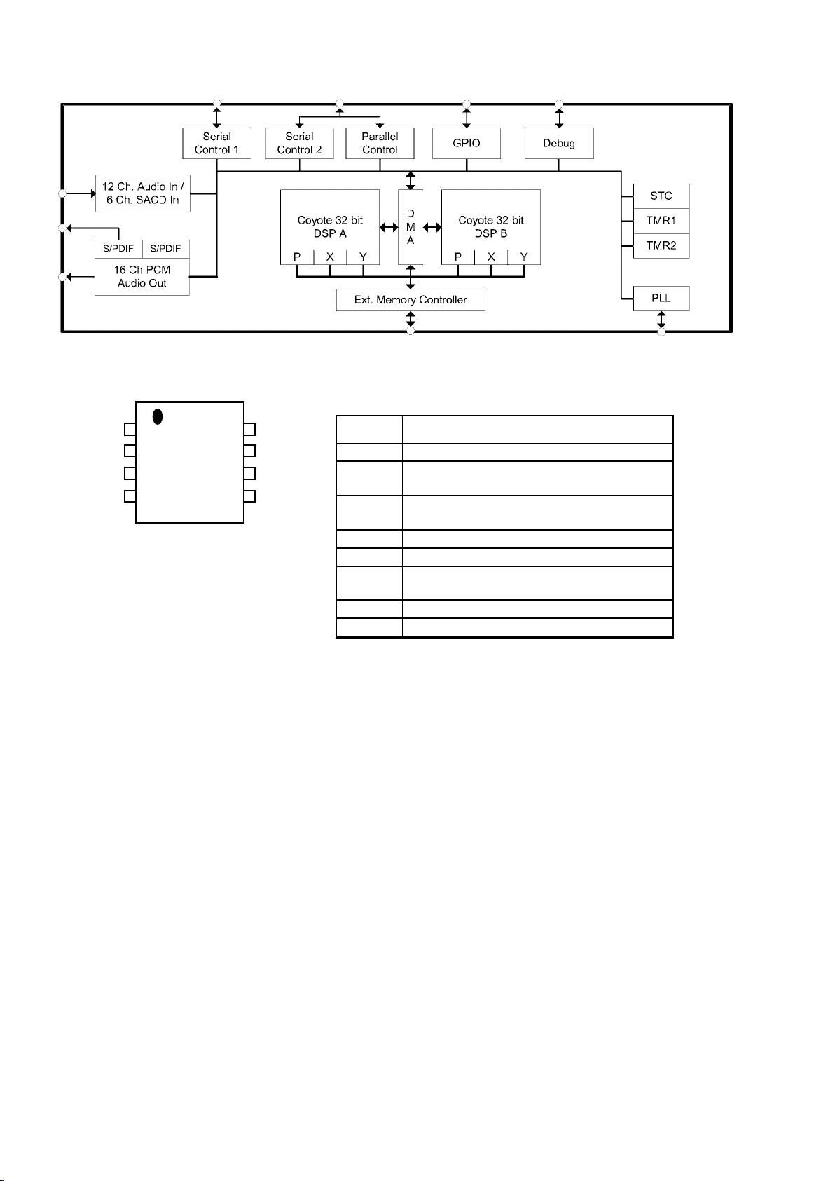
CS497024CVZ Block diagram
MX25L8006EM2I-12G (DIGITAL : IC742)
PIN DESCRIPTION
CS#
SO/SIO1
WP#
GND
1
2
3
4
8
7
6
5
VCC
HOLD#
SCLK
SI/SIO0
SYMBOL
CS#
SI/SIO0
SO/SIO1
SCLK
WP#
HOLD#
VCC
GND
DESCRIPTION
Chip Select
Serial Data Input (for 1 x I/O)/ Serial Data
Input & Output (for Dual Output mode)
Serial Data Output (for 1 x I/O)/ Serial Data
Output (for Dual Output mode)
Clock Input
Write protection
Hold, to pause the device without
deselecting the device
+ 3.3V Power Supply
Ground
94
Page 95

M12L16161A5TG (DIGITAL : IC743)
M12L16161A5TG Terminal Functions
Pin Name Input Function
CLK System Clock Active on the positive going edge to sample all inputs.
CS Chip Select
CKE Clock Enable
A0 ~ A10/AP Address
BA Bank Select Address
RAS Row Address Strobe
CAS Column Address Strobe
WE Write Enable Enables write operation and row precharge. Latches data in starting from CAS , WE active.
L(U)DQM Data Input / Output Mask
DQ0~15 Data Input / Output Data inputs/outputs are multiplexed on the same pins.
VDD/VSS Power Supply/Ground Power and ground for the input buffers and the core logic.
VDDQ/VSSQ Data Output Power/Ground Isolated power supply and ground for the output buffers to provide improved noise immunity.
N.C/RFU No Connection/ Reserved for Future Use This pin is recommended to be left No Connection on the device.
Disables or enables device operation by masking or enabling all inputs except CLK, CKE
and L(U)DQM.
Masks system clock to freeze operation from the next clock cycle.
CKE should be enabled at least one cycle prior to new command.
Disable input buffers for power down in standby.
Row / column addresses are multiplexed on the same pins.
Row address : RA0 ~ RA10, column address : CA0 ~ CA7
Selects bank to be activated during row address latch time. Selects bank for read/write
during column address latch time.
Latches row addresses on the positive going edge of the CLK with RAS low.
Enables row access & precharge.
Latches column addresses on the positive going edge of the CLK with CAS low.
Enables column access.
Makes data output Hi-Z, t
Blocks data input when L(U)DQM active.
after the clock and masks the output.
SHZ
95
Page 96

CS42528-CQ (DIGITAL : IC744)
CS42528 Block diagram
96
Page 97

CS42528 Terminal Functions
97
Page 98
TC74VHC157FT (DIGITAL : IC745-747)
TC74VHC157F/FN/FT/FK
Pin Assignment IEC Logic Symbol
A
A
Package Markings
Temp Rating (°C)
Package
Description
SELECT
1A
1
2
S G
15
V
CC
ST
(15)
(1)
EN
G1
16
ST
SELECT
4A
1B
1Y
2A
2B
2Y
GND
B A
3
Y B
4
5
6
7
8
Y
B A
Y BY
(top view)
14
13
12
11
10
9
4B
4Y
3A
3B
3Y
1A
1B
2A
2B
3A
3B
4A
4B
Truth Table
Inputs
ST SELECT A B
H X X X L
L L L X L
L L H X H
L H X L L
L H X H H
Output
(2)
(3)
(5)
(6)
(11)
(10)
(14)
(13)
1 MUX
1
(4)
(7)
(9)
(12)
1Y
2Y
3Y
4Y
X: Don’t care
EN5339QI (DIGITAL : IC751-753)
98
Page 99

NJU72340A (DIGITAL :IC761)
NJU72340A Terminal Functions
99
Page 100

BX8804(USB : IC901)
TDO / GP44
TMS / GP45
GP29 / CDDSP SCOR0
GP30 / CDDSP BCLK0
GP31 / CDDSP DATA0
GP32 / CDDSP LRCK0
GP35 / Timer0 Output / EXT INT 10
GP36 / EXT UCLK
TCK
GP33 / SBDT0
GP34
/ SBCK
RESETN
NTRST
VSS33
TEST
VDD33
VSS33
USBVDD33
USBDP
USBDM
USBVSS33
PLL3VSS12
PLL3VDD12
PLL2VSS12
PLL2VDD12
PLL1VSS12
PLL1VDD12
ADIN4
ADIN3
ADIN2
XI
XO
97
98
99
100
101
102
103
104
105
106
107
108
109
110
111
112
113
114
115
116
117
118
119
120
121
122
123
124
125
126
127
128
NT 9
VDD33
DMCK
DBCK
DLRCK
GP23 HUART1 DI
GP25 / EXT INT 5 / SPI2 CK
GP26 / EXT INT 6 / SPI2 MISO
GP27 / EXT INT 7 / SPI2 MOSI
GP28 / Wake-Up
TDI / GP43
VDD12
VSS12
919293
94
95
96
4
3
2
1
GP22 / CS2 / EXT INT 4
GP24 / HUART1 DO
86
878889
90
11
1098
765
DDATA
VSS33
GP21 / EXT INT 3 / SPI2 CS
GP20 / SPI1 MOSI
80
81
82
838485
BX8804
17
16
15
141312
GP18 / SPI1 CK
GP19 / SPI1 MISO
777879
201918
GP14 / UART0 TX / EXT I
GP15 / UART1 RX / I2C SCL
GP16 / UART1 TX / I2C SDA
GP17 / SPI1 CS
707172
73
747576
272625
24
232221
GP07 / SPI0 MOSI
GP08 / HUART0 DI
GP06 / SPI0 MISO
65
66
676869
GP05 / SPI0 CK
64
GP04 / SPI0 CS
63
GP03 / EXT Clock
62
ECSN
61
EOEN / GP42
60
EWEN / GP41
59
EAD20 / GP40 / Boot Mode
58
EAD19 / GP39
57
EAD18 / GP38
56
EAD17 / GP37
55
WEN
54
CASN
53
SDCLK
52
VSS33
51
VDD33
50
RASN
49
CKE
48
VSS12
47
VDD12
46
SDCSN
45
UDQM
44
LDQM
43
BA1
42
BA0
41
AD12
40
AD11
39
AD10
38
AD09
37
AD08
36
AD07
35
AD06
34
AD05
33
32
31
302928
GP10 / HUART0 RTS / EXT INT 11
GP11 / HUART0 CTS / EXT INT 12
GP09 / HUART0 DO
GP12 / CS1
GP13 / UART0 RX / EXT INT 8
ADIN0
ADIN1
AVDD33
D0
AVSS33
GP01 / EXT INT 1
GP00 / EXT INT 0
D10
NC
VSS12
VDD12
D5
D4
D12
D11
D7
D15
D14D6D13
AD02
AD01
AD00
AD04
AD03
VSS33
VDD33
D3
D2
D9D1D8
100
 Loading...