

Page 1
For U.S.A., Canada, Europe,
Asia, China, Taiwan R.O.C.
& Korea model
SERVICE MANUAL
MODEL AVR-1404/484
AV SURROUND RECEIVER
Ver. 2
●
For purposes of improvement, specifications and
design are subject to change without notice.
●
Please use this service manual with referring to the
operating instructions without fail.
●
Some illustrations using in this service manual are
slightly different from the actual set.
注 意
サービスをおこなう前に、このサービスマニュアルを
必ずお読みください。本機は、火災、感電、けがなど
に対する安全性を確保するために、さまざまな配慮を
おこなっており、また法的には「電気用品安全法」に
もとづき、所定の許可を得て製造されております。
従ってサービスをおこなう際は、これらの安全性が維
持されるよう、このサービスマニュアルに記載されて
いる注意事項を必ずお守りください。
●
本機の仕様は性能改良のため、予告なく変更すること
があります。
●
補修用性能部品の保有期間は、製造打切後8年です。
●
修理の際は、必ず取扱説明書を参照の上、作業を行っ
てください。
●
本文中に使用しているイラストは、説明の都合上現物
と多少異なる場合があります。
16-11, YUSHIMA 3-CHOME, BUNKYO-KU, TOKYO 113-0034 JAPAN
X0172V.02 DE/CDM 0309
Page 2
SAFETY PRECAUTIONS
The following check should be performed for the continued protection of the customer and service technician.
LEAKAGE CURRENT CHECK
Before returning the unit to the customer, make sure you make either (1) a leakage current check or (2) a line to chassis
resistance check. If the leakage current exceeds 0.5 milliamps, or if the resistance from chassis to either side of the
power cord is less than 460 kohms, the unit is defective.
500V
1M
2AVR-1404/484
(1)
(2)
(1)
(2)
2
Page 3
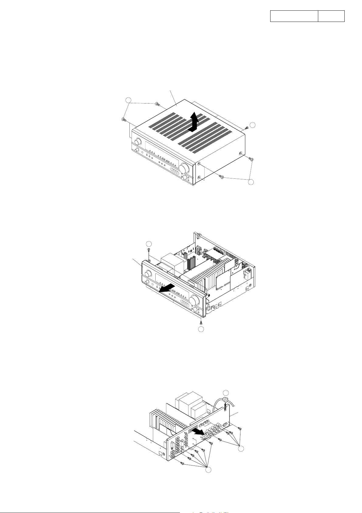
DISASSEMBLY
(Follow the procedure below in reverse order when reassembling.)
1. Top Cover
(1) Remove 6 screws ① and 3 screws ② , detach the Top cover in the arrow direction.
Top Cover
1
3AVR-1404/484
2
1
2. Front Panel
(1) Remove 4 screws ③ and 2 screws ④ .
(2) Detach the Front Panel in the arrow direction.
4
Front Panel
3. Rear Panel
(1) Remove cord bushing ⑤ from the Rear Panel.
(2) Remove 30 screws ⑥ .
(3) Detach the Rear Panel in the arrow direction.
3
5
Rear Panel
6
6
3
Page 4
LEVEL DIAGRAMS (1/2)
4AVR-1404/484
DIGITAL
CD IN
6CH IN
40dB
30dB
20dB
10dB
6CH IN (200mV)
-
-
0dB
10dB
20dB
6CH IN
CD IN
INPUT
BUFFER
AMP
FRONT
-
12dB
/
D IN
A
REV AMP
A
/
D IN
REV AMP
-
-
-
0dBFS
10dBFS
20dBFS
30dBFS
M62446
ELECTRIC
VOLUME
-
18dB
PRE AMP
MUTE
15.5dB
VOL 00
POWER AMP
25.5dB
-
35.5dB
ATT
SPK OUT
FRONT
/
P OUT
H
SPK OUT
FRONT
2.83V
/
8ohm)
(1W
/
P OUT
H
47mV
(0.27W 8ohm)
/
A OUT
D
LPF
HPF
DIR
A
/
D
A
/
D
DSP
-
10dBFS
-
20dBFS
-
30dBFS
D
0dBFS
/
A
MUTE
D
/
A
6dB
/
A OUT
D
100mV REF
REV AMP
SW SUM
REV AMP
SUM S
TONE
/
W
6CH IN
6CH IN
40dB
30dB
20dB
10dB
(200mV)
-
-
0dB
10dB
20dB
CENTER
SURROUND
DSP OUT
-
10dBFS
-
20dBFS
-
30dBFS
D
0dBFS
/
A
M62446
MUTE
25.5dB
-
18dB
VOL 00
15.5dB
D
/
A
D
/
A OUT
100mV REF
MUTE
6dB
SPK OUT
CENTER
SURROUND
SPK OUT
2.83V
(1W
/
8ohm)
4
Page 5
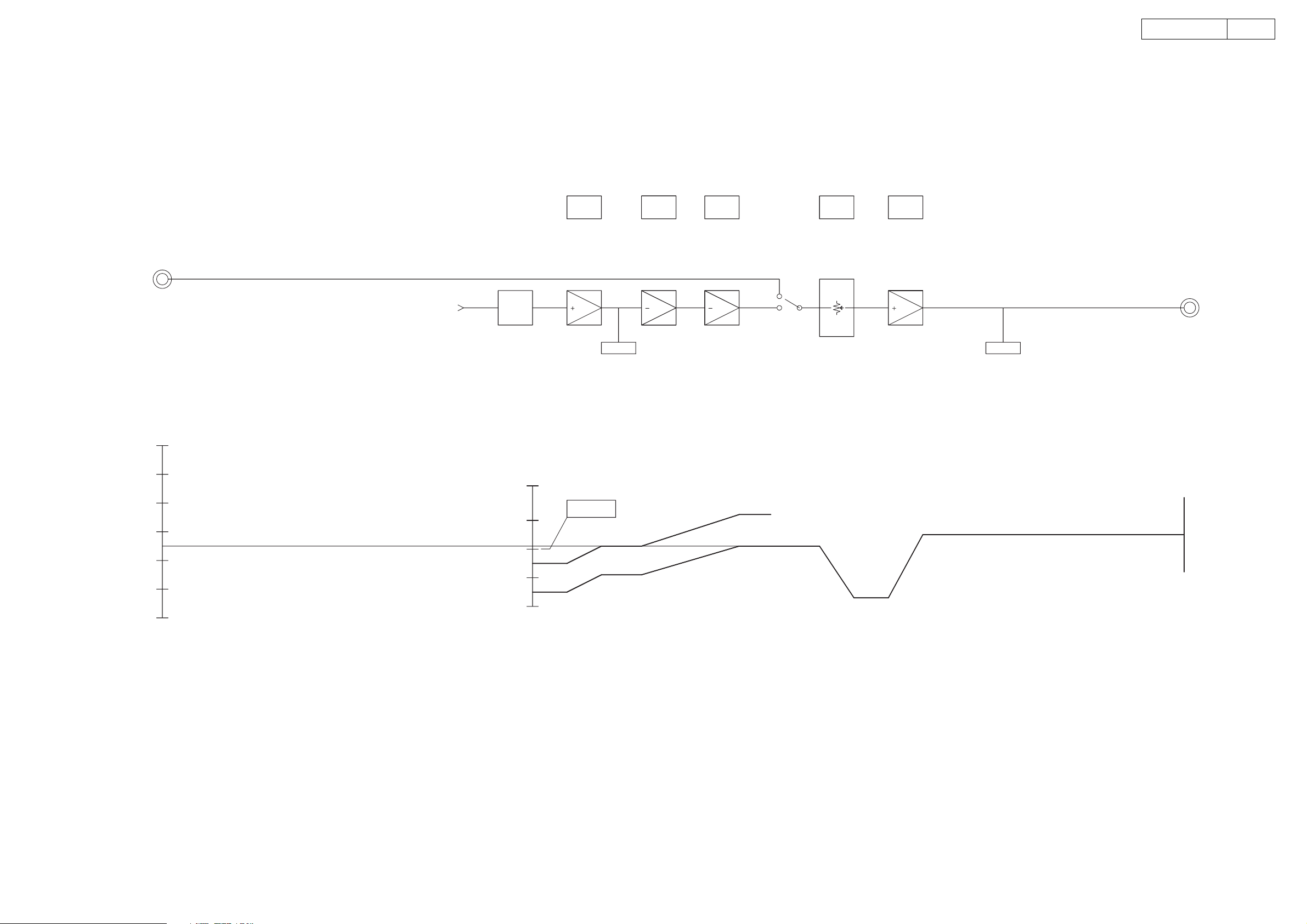
LEVEL DIAGRAMS (2/2)
5AVR-1404/484
SUB_WOOFER
6CH INPUT
(200mV)
6CH IN
(112mV)
-
18dB
ELECTRIC
VOLUME
M62446
VOL 00
PRE AMP
25.5
(
15.5+5+5)dB
MUTE
SUB WOOFER
PRE OUT
SUB WOOFER
PRE OUT
150mV
/
A OUT
D
LPF
D
/
-
10dBFS
-
-
-
-
35dBFS
0dBFS
20dBFS
25dBFS
30dBFS
A
MUTE
/
A
D
/
A Out
Front D
200mV ref
LFE
LFE
6dB
6dB
DSP OUT
30dB
20dB
10dB
0dB
-
5dB
-
10dB
-
20dB
-
30dB
Config2
Config1
REV AMP
SW SUM
REV AMP
TO FRONT CH
10.5dB
5dB
5
Page 6
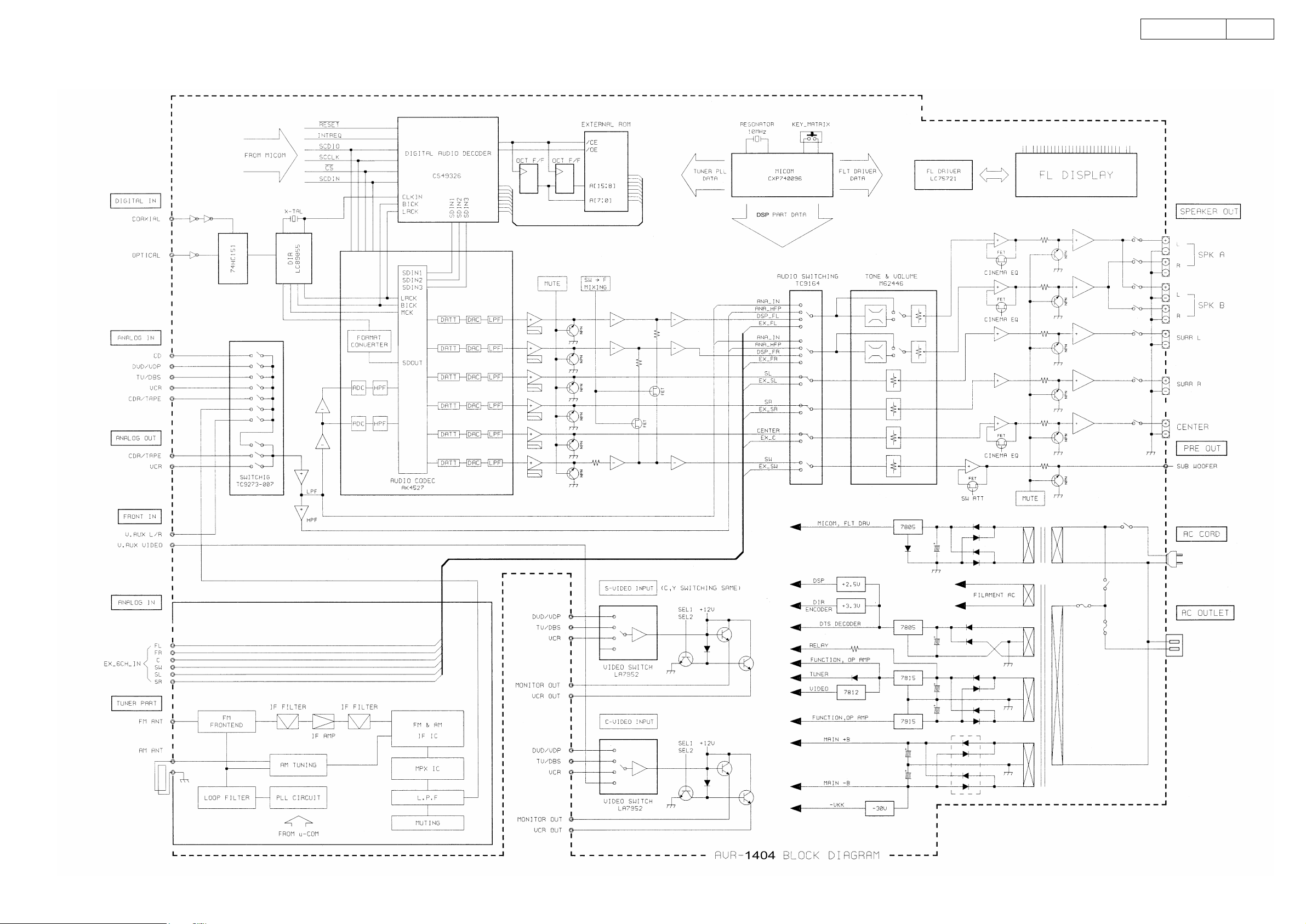
BLOCK DIAGRAM
6AVR-1404/484
6
Page 7
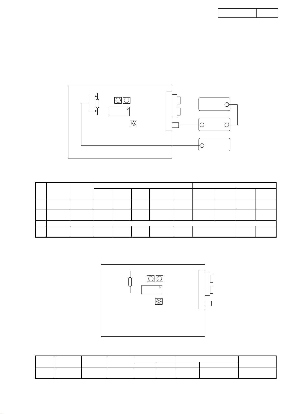
ADJUSTMENT
Tuner Section
CONNECTION DIAGRAM OF MEASURING INSTRUMENTS
FM
T402 T403
R471
IC402
7AVR-1404/484
STEREO
MODULATOR
VR402
TUNER B'D
FM ALIGNMENT
Alignment
Step
AM
Item
Center
1
Adjustment
2 Distortion
3 Repeat Steps 1 and 2
4 Signal Level
Tuning
Frequency
Setting
98.1MHz
(98.0MHz)
98.1MHz
(98.0MHz)
98.1MHz
(98.0MHz)
Type Frequency
FM SSG 98.1MHz 60dBP
FM SSG 98.1MHz 60dBP
FM SSG 98.1MHz 20dBP OFF
Input Output Adjustment
Input
Level
Modulation Coupling Type Connect to Points Adjust to
Mono
1kHz 100%
Mono
1kHz 100%
75ohm
Antenna
Terminal
Antenna
Terminal
Antenna
Terminal
FM SSG
Digital
Voltmeter
Digital
Voltmeter
Distortion
Meter
Light “TUNED” on
Terminal (L)
FL Display
R471 T402 r 50mV
Output
T403
VR402
Minimum
Distortion
+14
20
−10
dB
AM ALIGNMENT
Step
1 Signal Level
Alignment
Item
Frequency Input
999 (1000)
kHz
AM SSG VR401
T402 T403
R471
IC402
VR401
TUNER B’D
Output Adjustment
Type Connect to Points Adjust to
Light “TUNED” on
7
FL Display
Remarks
SSG OUTPUT
74dBP (EMF)
Page 8
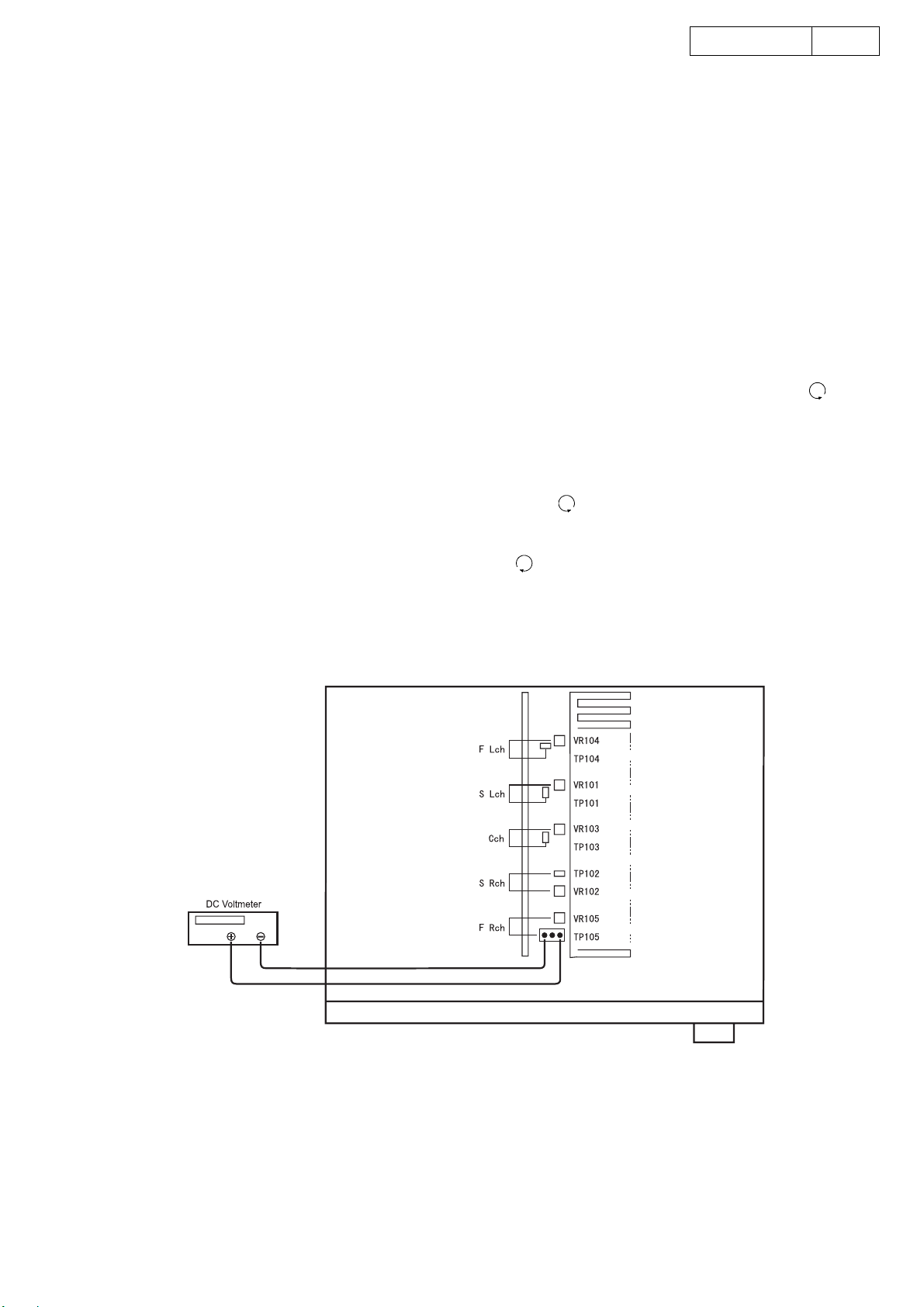
Audio Section
Idling Current
Required measurement equipment : DC Voltmeter
Preparation
(1) Avoid direct blow from an air conditioner or an electric fan, and adjust the unit at normal room tempereture
15 °C ~ 30 °C (59 °F ~ 86 °F).
(2) Presetting
● POWER (Power sourse switch) → OFF
● SPEAKER (Speaker terminal) → No load (Do not connect speaker, dummy resistor, etc.)
Adjustment
(1) Remove top cover and set VR101, VR102, VR103, VR104, VR105 on Amp. Unit at full counterclockwise ( )
position.
(2) Connect DC Voltmeter to test points (FRONT-Lch: TP104, FRONT-Rch: TP105, CENTER ch: TP103,
SURROUND-Lch: TP101, SURROUND-Rch: TP102).
(3) Connect power cord to AC Line, and turn power switch "ON".
8AVR-1404/484
(4) Presetting. MASTER VOLUME : "---" counterclockwise (
MODE : 5CH STEREO
FUNCTION : CD
(5) Within 2 minutes after the power on, turn VR101 clockwise (
DC.
(6) After 10 minutes from the preset above, turn VR101 to set the voltage to 2.5 mV ±0.5 mV DC.
(7) Adjust the Variable Resistors of other channels in the same way.
min.)
) to adjust the TEST POINT voltage to 1.5 mV ±0.5 mV
8
Page 9
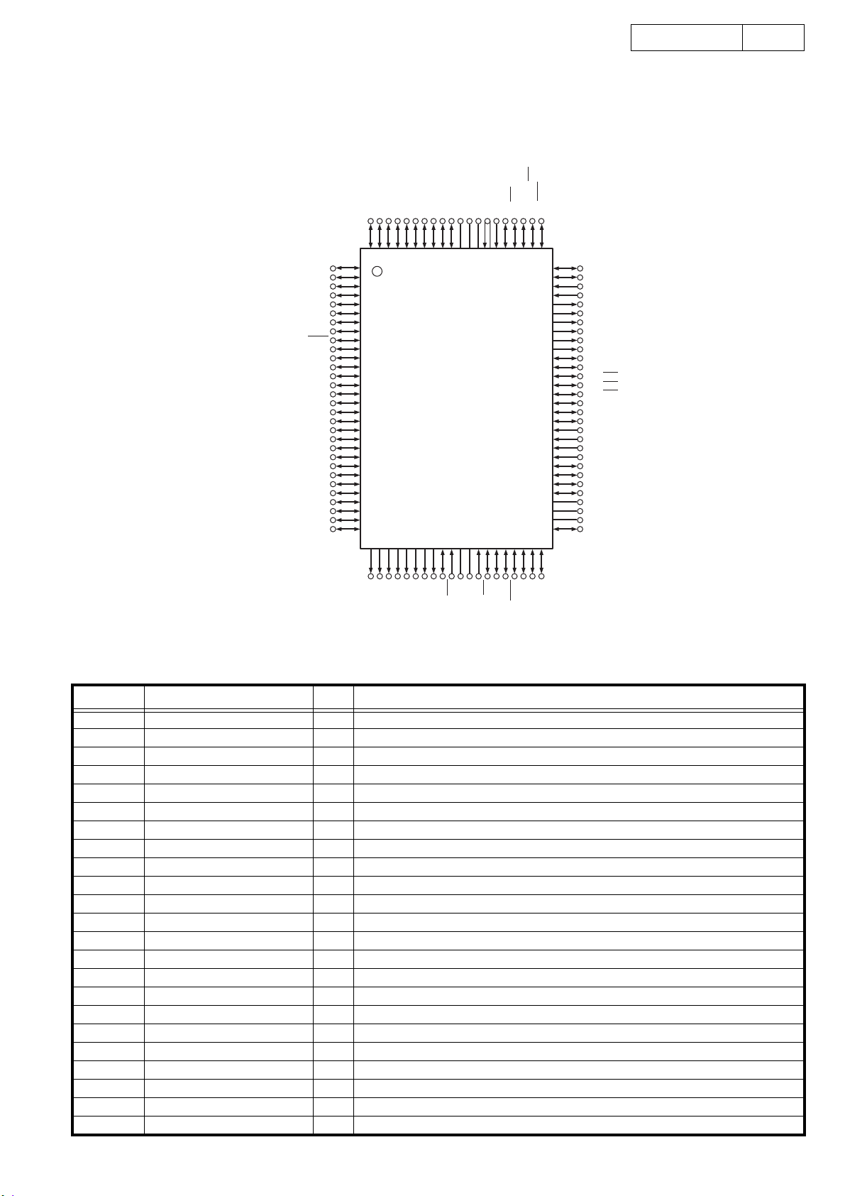
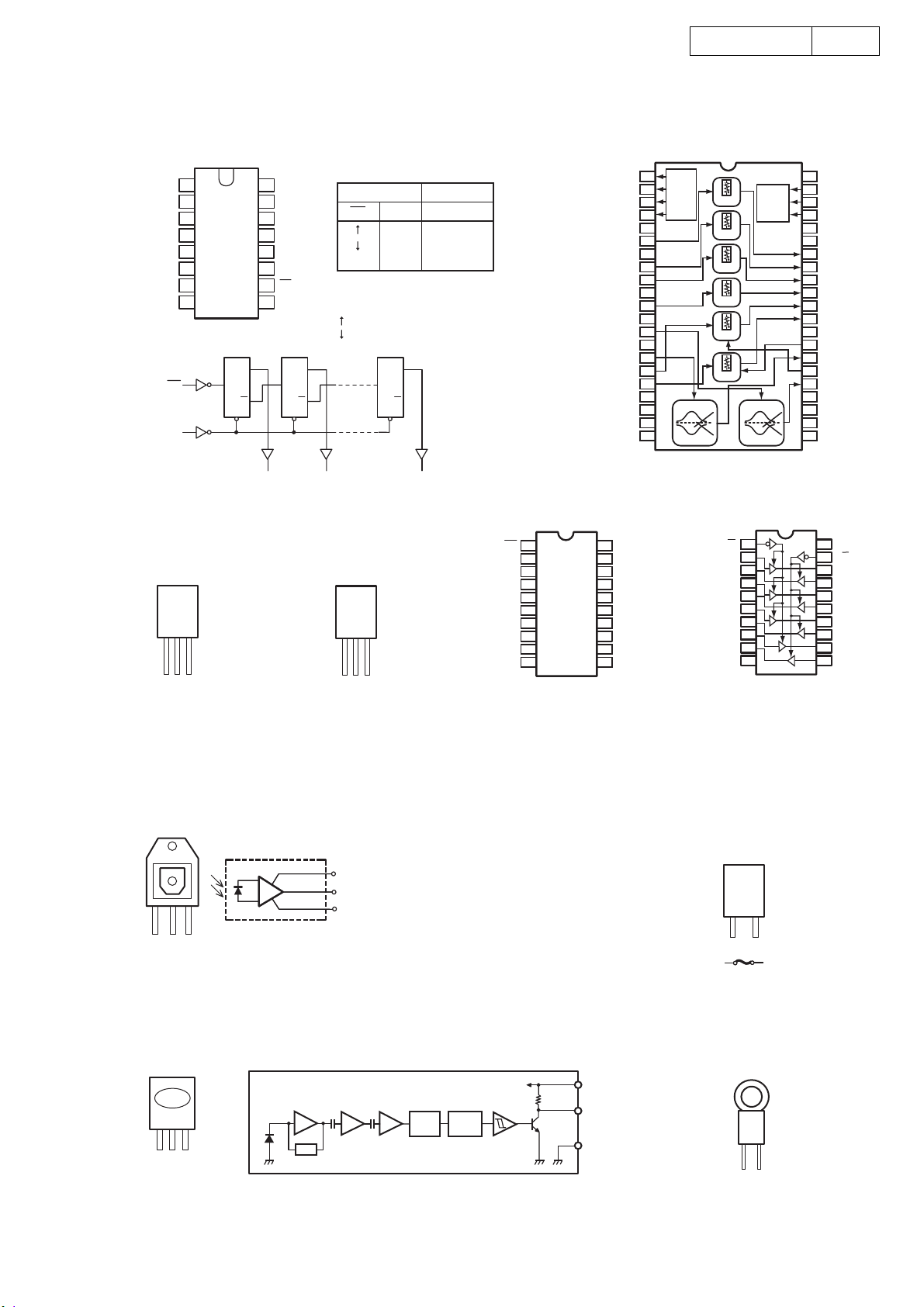
SEMICONDUCTORS
IC’s
CXP740096
(IC201)
PC6
PC7
9AVR-1404/484
DDVSS
PK1/TX
PK2/TEX
PI1/RMC
PI2/NMI
PI3/TO0/ADJ
PI4/INT1/CS1
PA0
PA1
PA2
PA3
PA4
PA5
PA6
PA7NCV
PI5/SCK1
CXP740096 Terminal Function
PC5
PC4
PC3
PC2
PC1
PC0
PB7/SI2
PB6/SO2
PB5/SCK2
PB4/TO2
PB3
PB2
PB1
PB0
PJ7
PJ6
PJ5
PJ4
PJ3
PJ2
PJ1
PJ0
PD7
PD6
PD5
PD4
PD3
PD2
PD1
PD0
999897969594939291
100
1
2
3
4
5
6
7
8
9
10
11
12
13
14
15
16
17
18
19
20
21
22
23
24
25
26
27
28
29
30
31
32333435363738394041424344454647484950
PH7
PH6
PH5
PH4
PH3
PH2
908988878685848382
TOP VIEW
SS
V
PH1
PH0
RST
XTAL
PK7/TO1
EXTAL
PK5/SI0
PK6/CS0
PK4/SO0
PF7/AN11
PK3/SCK0
81
80
79
78
77
76
75
74
73
72
71
70
69
68
67
66
65
64
63
62
61
60
59
58
57
56
55
54
53
52
51
PF5/AN9
PF6/AN10
PI6/SO1
PI7/SI1
PE0/INT0
PE1/INT2
PE2/PWM0
PE3/PWM1
PE4
PE5
PE6
PE7
PG0/TxD
PG1/RxD
PG2/EC0
PG3/EC1
PG4/EC2
PG5/INT3
PG6/INT4
PG7/CINT
AN0
AN1
AN2
AN3
PF0/AN4
PF1/AN5
PF2/AN6
PF3/AN7
AV
DD
AV
REF
AV
SS
PF4/AN8
Pin No. Pin Name I/O Function
1 9273 STB O TC9273 CONTROL
2 9273 9164 CLK O TC9273/TC9164 CONTROL
3 9273 9164 DAT O TC9273/TC9164 CONTROL
4 SW SUM O SW SUMMING CONTROL
5 SEL. CLK O SEL. CLK
6 ERR MUTE O ERR MUTE
7 89055 AUTO O LC89055 CONTROL
8 89055 AUDIO I LC89055 CONTROL
9 89055 EMPHA I LC89055 CONTROL
10 SRAM CE O SRAM (IC833) CONTROL
11 49326 ABOOT O CS49326 CONTROL
12 ROM 3 O ROM (IC807) CONTROL
13 ROM 30 O ROM (IC807) CONTROL
14 ROM 2 O ROM (IC807) CONTROL
15 49326 RST O CS94326 RESET
16 49326 CE O CS94326 CE
17 SCLK O LC89055/AK4527/CS49326 CLOCK
18 89055 CE O LC89055 CE
19 4527 CE O AK4527 CE
20 4527 RST O AK4527 RESET
21 9164 ST O TC9164 CONTROL
22 SW MUTE O SW MUTE
23 RELAY FRONT B O FRONT B RELAY
9
Page 10
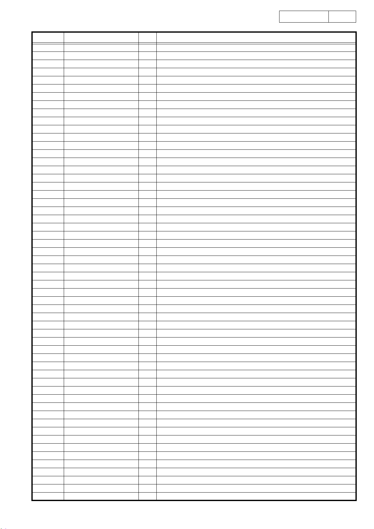
Pin No. Pin Name I/O Function
24 RELAY FRONT A O FRONT A RELAY
25 RELAY SURR O SURROUND RELAY
26 RELAY CNT O CENTER RELAY
27 RELAY H/P O H/P RELAY
28 RELAY POWER O POWER RELAY
29 CNT MUTE O CENTER MUTE
30 FRONT MUTE O FRONT MUTE
31 VIDEO MUTE O VIDEO MUTE
32 SURR MUTE O SURROUND MUTE
33 NC
34 FL DRV RST O LC75721NE RESET
35 NC
36 NC
37 NC
38 SW ATT CTRL O SW. ATT. CONTROL
39 CINE EQ CTRL O CINEMA EQ. CONTROL
40 RESET I RESET
41 GND I
42 XTAL
43 EXTAL
44 FL DRV CE O LC75721NE CE
45 FL DRV DATA O LC75721NE DATA
46 FL DRV/2090 CLK O CONTROL CLOCK
47 2090 DATA O BU2090F DATA
48 VOL DOWN I ENCODER INPUT (VOLUME)
49 VOL UP I ENCODER INPUT (VOLUME)
50 SEL DOWN I ENCODER INPUT (SELECT)
51 SEL UP I ENCODER INPUT (SELECT)
52 AV
53 V
54 AV
55 NC
56 GND
57 STEP OPT I AREA SELECT
58 SET OPT I MODEL SELECT
59 GND
60 KEY IN3 I KEY INPUT
61 KEY IN2 I KEY INPUT
62 KEY IN1 I KEY INPUT
63 9K/10K STEP I TUNER STEP SELECT
64 PROTECT I PROTECTION
65 89055 RST O LC89055 RESET
66 SDIN I LC89055/AK4527/CS49326 DATA INPUT
67 SDIO O LC89055/AK4527/CS49326 SDIO
68 ROM CE O ROM (IC807) CONTROL
69 FUNC DOWN I ENCODER INPUT (FUNCTION)
70 FUNC UP I ENCODER INPUT (FUNCTION)
71 NC
72 NC
73 NC
74 NC
75 NC
76 NC
77 PWR DOWN I POWER DOWN DETECT
78 RDS CLK I TDA7330 CONTROL CLOCK
79 RDS DATA I TDA7330 CONTROL DATA
SS
REF
DD
-
-
-
-
-
-
-
-
-
-
-
-
-
-
-
-
-
-
10AVR-1404/484
10
Page 11
Pin No. Pin Name I/O Function
80 NC
81 NC
82 49326 INTREQ I CS49326 INTREQ
83 74HC151 A0 O IC832 CONTROL
84 74HC151 A1 O IC832 CONTROL
85 REMOCON I REMOTE CONTROL SIGNAL INPUT
86 GND
87 GND
88 V
89 V
90 NC
91 M62446 CE O M62446 CONTROL
92 PLL DATA O M62446/PLL CONTROL
93 PLL CLK O M62446/PLL CONTROL
94 PLL DT IN I PLL CONTROL
95 TU MUTE O TUNER MUTE
96 STEREO I STEREO DETECT
97 TUNED I TUNED DETECT
98 PLL CE O PLL CONTROL
99 SEL 2 O LA7952 CONTROL (VIDEO)
100 SEL 1 O LA7952 CONTROL (VIDEO)
SS
DD
-
-
-
-
-
-
VDD BACK UP
-
11AVR-1404/484
11
Page 12
12AVR-1404/484
CS49326-CL
(IC812)
CS49326-CL Terminal Function
Pin
No.
Pin Name
A0,SCCLK
DATA7,EMAD7,GPIO7
DATA6,EMAD6,GPIO6
DATA5,EMAD5,GPIO5
DATA4,EMAD4,GPIO4
DATA3,EMAD3,GPIO3
DATA2,EMAD2,GPIO2
DATA1,EMAD1,GPIO1
DATA0,EMAD0,GPIO0
DGND2
A1,SCDIN
RD,R/W,EMOE,GPIO11
WR,DS,EMWR,GPIO10
AUDATA3,XMT958
DGND1
VD1
MCLK
SCLK
LRCLK
AUDATA0
AUDATA1
44
56
SCDIO,SCDOUT,PSEL,GPIO9
21 22
ABOOT,INTREQ
1234
SDATAN1
EXTMEM,GPIO8
7
8
9
10
11
VD2
12
13
14
15
16
17
18 19 20
CS
43
VD3
DGND3
SCLKN1,STCCLK2
LRCLKN1
404142
282726252423
CMPCLK,SCLKN2
CMPDAT,SDATAN2,RCV958
39
AUDATA2
38
DC
37
DD
RESET
36
AGND
35
34
VA
FILT1
33
32
FILT2
CLKSEL
31
CLKIN
30
CMPREQ,LRCLKN2
29
Function
1 VD1 Digital positive supply
2 DGND1 Digital supply ground
3 AUDATA3, XMT958 SPDIF transmitter output, Digital audio output 3
4 WR, DS, EMWR, GPIO10 Host write strobe or host data strobe or external memory write enable or general purpose input & output number 10
5 RD, R/W, EMOE, GPIO11
Host parallel output enable or host parallel R/W or external memory output enable or general purpose input & output number11
6 A1, SCDIN Host address bit one or SPI serial control data input
7 A0, SCCLK Host parallel address bit zero or serial control port clock
8 DATA7, EMAD7, GPIO7
9 DATA6, EMAD6, GPIO6
10 DATA5, EMAD5, GPIO5
11 DATA4, EMAD4, GPIO4
12 VD2 Digital positive supply
13 DGND2 Digital supply ground
14 DATA3, EMAD3, GPIO3
15 DATA2, EMAD2, GPIO2
16 DATA1, EMAD1, GPIO1
17 DATA0, EMAD0, GPIO0
18 CS Host parallel chip select, host serial SPI chip select
19 SCDIO, SCDOUT, PSEL, GPIO9 Serial control port data input and output, parallel port type select
20 INTREQ, ABOOT Control port interrupt request, automatic boot enable
21 EXTMEM, GPIO8 External memory chip select or general purpose input & output number 8
22 SDATAN1 PCM audio data input number one
23 VD3 Digital positive supply
24 DGND3 Digital supply ground
25 SCLKN1, STCCLK2 PCM audio input bit clock
26 LRCLKN1 PCM audio input sample rate clock
27 CMPDAT, SDATAN2, RCV958 PCM audio data input number two
28 CMPCLK, SCLKN2 PCM audio input bit clock
29 CMPREQ, LRCLKN2 PCM audio input sample rate clock
30 CLKIN Master clock input
31 CLKSEL DSP clock select
32 FILT2 Phase locked loop filter
33 FILT1 Phase locked loop filter
34 VA Analog positive supply
35 AGND Analog supply ground
36 RESET Master reset input
37 DD Reserved
38 DC Reserved
39 AUDATA2 Digital audio output 2
40 AUDATA1 Digital audio output 1
41 AUDATA0 Digital audio output 0
42 LRCLK Audio output sample rate clock
43 SCLK Audio output bit clock
44 MCLK Audio master clock
12
Page 13
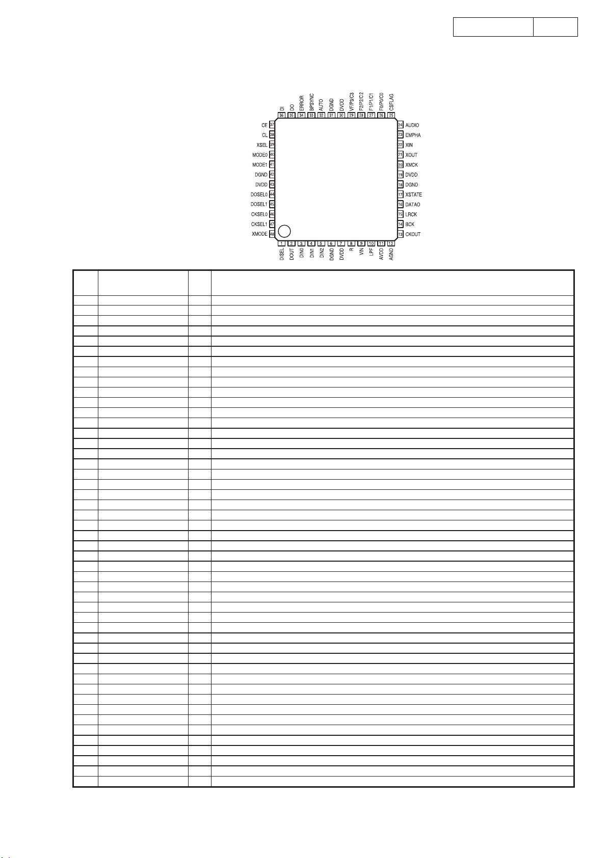
LC89055W (IC810)
LC89055W Terminal Function
Pin
No.
1 DISEL I Data input terminal (select input pin of DIN0, DIN1)
2 DOUT O Input bi-phase data through output terminal
3 DIN0 I Amp built-in coaxial/optical input correspond data input terminal
4 DIN1 I Amp built-in coaxial/optical input correspond data input terminal
5 DIN2 I Optical input correspond data input terminal
6 DGND Digital GND
7 DVDD Digital power supply
8 R I VCO gain control input terminal
9 VIN I VCO free-run frequency setting input terminal
10 LPF O PLL loop filter setting terminal
11 AVDD Analog power supply
12 AGND Analog GND
13 CKOUT O Clock output terminal (256fs, 384fs, 512fs, X’tal osc., VCO free-run osc.)
14 BCK O 64fs clock output terminal
15 LRCK O fs clock output terminal (L: Rch, H: Lch, I2S: Reverse)
16 DATAO O Data output terminal
17 XSTATE O Input data detecting result output terminal
18 DGND Digital GND
19 DVDD Digital power supply
20 XMCK O X’tal osc. clock output terminal (24.576MHz or 12.288MHz)
21 XOUT O X’tal osc. connection output terminal
22 XIN I X’tal osc. connection input terminal, external signal input possible (24.576MHz or 12.288MHz)
23 EMPHA O Emphasis information output terminal of channel status
24 AUDIO O Bit1 output terminal of channel status
25 CSFLAG O Top 40bit revise flag output terminal of channel status
26 F0/P0/C0 O Input fs cal. sig. out/data type out/input word inf. output terminal
27 F1/P1/C1 O Input fs cal. sig. out/data type out/input word inf. output terminal
28 F2/P2/C2 O Input fs cal. sig. out/data type out/input word inf. output terminal
29 VF/P3/C3 O Validity flag out/data type out/input word inf. output terminal
30 DVDD Digital power supply
31 DGND Digital GND
32 AUTO O Non PCM burst data transfer detect sig. output terminal
33 BPSYNC O Non PCM burst data preamble Pa, Pb, Pc, Pd sync sig. output terminal
34 ERROR O PLL lock error, data error flag output terminal
35 DO O CPU/IFD read data output terminal
36 DI I CPU I/F write data input terminal
37 CE I CPU I/F chip enable input terminal
38 CL I CPU I/F chip enable input terminal
39 XSEL I Frequency select input pin of XIN X’tal osc. (24.576MHz or 12.288MHz)
40 MODE0 I Mode setting input terminal
41 MODE1 I Mode setting input terminal
42 DGND Digital GND
43 DVDD Digital power supply
44 DOSEL0 I Data output format select input terminal
45 DOSEL1 I Data output format select input terminal
46 CKSEL0 I Output clock select input terminal
47 CKSEL1 I Output clock select input terminal
48 XMODE I Reset input terminal
For latch-up countermeasure, set digital (DVDD) and analog (AVDD) power on/off in the same timing.
Pin Name FunctionI/O
13AVR-1404/484
13
Page 14
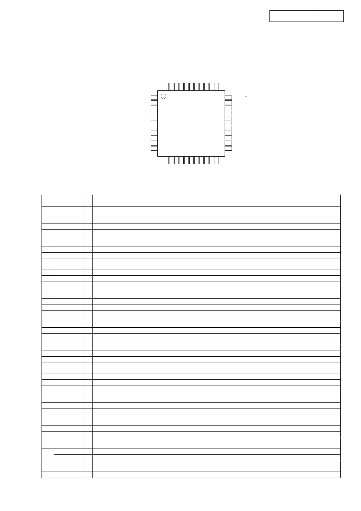
AK4527BVQ (IC813)
L0OP1
L0OP0/SDA/CDTI
444342
DIF1/SCL/CCLK
DIF0/CSN
P/S
MCLK
39
38
40
41
DZF1
37
AVSS
36
AVDD
35
VCOM
VREFH
34
14AVR-1404/484
22
CAD1
CAD0
33
DZ F2/OVF
32
RIN+
31
RIN–
30
LIN+
29
LIN–
28
ROUT1
27
LOUT1
26
ROUT2
25
LOUT2
24
ROUT3
23
LOUT3
SDOS
I2C
SMUTE
BICK
LRCK
SDTI1
SDTI2
SDTI3
SDTO
DAUX
DFS
1
2
3
4
5
6
7
8
9
10
11
12
13 14
NC
AK4527BVQ
15
TVDD
DZ FE
Top View
16 17 18
PDN
DVSS
DVDD
192021
NC
TST
ADIF
AK4527BVQ Terminal Function
Pin
Pin Name I/O Function
No.
1 SDOS I SDTO source select pin, L: Internal ADC output, H: DAUX input
2 I2C I Serial control mode select pin, L: 3-core serial, H: I2C bus
3 SMUTE I Soft mute pin, H: Soft mute start, L: Release
4 BICK I Audio serial data clock pin
5 LRCK I Input channel clock pin
6 SDTI1 I DAC1 audio serial data input pin
7 SDTI2 I DAC2 audio serial data input pin
8 SDTI3 I DAC3 audio serial data input pin
9 SDTO O Audio serial data output pin
10 DAUX I Auxiliary audio serial data input pin
11 DFS I Double speed sampling mode pin, L: Normal, H: Double
12 NC No Connect, No internal bonding
13 DZFE I Zero input detect enable pin
14 TVDD Power pin for output buffer, 2.7V~5.5V
15 DVDD Digital power pin, 4.5V~5.5V
16 DVss Digital GND pin, 0V
17 PDN I Power down & reset pin, L: Powered-down and register initialized, Reset with PDN when switching P/S or CAD0-1
18 TST I Test pin, connected to DVSS
19 NC No Connect, No internal bonding
20 ADIF I Analog Input Format Select pin
21 CAD1 I Chip address-1 pin
22 CAD0 I Chip address-0 pin
23 LOUT3 O DAC3L channel analog out pin
24 ROUT3 O DAC3R channel analog out pin
25 LOUT2 O DAC2L channel analog out pin
26 ROUT2 O DAC2R channel analog out pin
27 LOUT1 O DAC1L channel analog out pin
28 ROUT1 O DAC1R channel analog out pin
29 LIN- I L-ch analog inverted input pin
30 LIN+ I L-ch analog non-inverted input pin
31 RIN- I R-ch analog inverted input pin
32 RIN+ I R-ch analog non-inverted input pin
33 DZF2/OVF O 0 input detect 2 pin/Analog input overflow detect pin
34 VCOM O Common V-out pin, AVDD/2, connect large capacitor to avoid noise
35 VREFH I Ref. V input pin, AVDD
36 AVDD Analog GND pin, 4.5V~5.5V
37 AVss Analog GND pin, 0V
38 DZF1 O 0 input detect pin, H: Input data of G1 is 8192 times “0” in a raw or RSTN bit “0”
39 MCLK I Master clock input pin
40 P/S I Parallel/Serial select pin, L: Serial control
DIF0 I Audio data I/F format 0 pin (parallel control)
41
CSN I Chip select pin (3-wire serial control), connect to DVDD when I
DIFI I Audio data I/F format 1 pin (parallel control)
42
SCL/CCLK I Control data clock pin (serial control), I
LOOP0 I Loop back mode 0 pin (parallel control), effects digital loop back ADC to all DAC
43
SDA/CDTI I/O Control data input pin (serial control), I
2
C=”L”: CCLK (3-wire serial), I2C=”H”: SCL (I2C bus)
2
C=”L”: CCTI (3-wire serial), I2C =”H” SDA (I2C bus)
44 LOOP1 I Loop back mode 1 pin, from SDT1 to all DAC
2
C bus control
14
Page 15
15AVR-1404/484
LC72131 (IC401)
1
X I N
C E
2
D I
3
C L
4 1 7
D O
5
B O 1
6
B O 2
7
B O 3
8
B O 4
9 1 2
I O 1
1 0 1 1
LA1266 (IC402)
A M - I F F M - I F F M - I N
11
18
13
10
I F
I F
B U F F E R
O S C
23
A M - I N
20
21
B U F F E R
R F M I X
R E G
22
124
X O U T
2 0
V s s
1 9
A O U T
1 8
A I N
P D
1 6
V D D
1 5
F M I N
1 4
12 13
1
F M - I F
A M - I F D E T
O S C
B U F F E R
G N D
24
4
2
N A R R O W
S - M E T E R
14
3
5
6
7
V c c
P O S T
Q . D .
A M P
A G C
S - M E T E R
17
19
16
L E D
D R I V E R
12
9
15
8
LA3401 (IC403)
22
V O L
R E G
S Y M M E T R I C A L
R E O C T A N C E
C I R C U I T
M U T I N G
21
O S C
F F
A M I N
1 3
I O 2
I F I N
F M A M C H A N G E
20
P H A S E
C O M P A R A T O R
F F
R o
19
F F
3 8 k H z
D E C O D E R
V C O S T O P
R c
R c
18
3 8 k H z 9 0 °
R b
F F
17
P I L O T D E T
1 9 k H z 9 0 °
R b
16
F F
M U T I N G C O N T R O L
F M A M C H A N G E O V E R
15
V c c O N
M U T I N G
14
13
L A M P
D R I V E R
T R I G G E R
S T E R E O
S W I T C H
M U T I N G
O U T P U T
12
BU2090F (IC302)
1
VSS
DATA
CLOCK
LCK
Q0
Q1
Q2
Q3
Q4
2
3
4
5
6
7
8
9
CONTROL CIRCUIT
12-bit SHIFT RESISTER
12-bit STRAGE RESISTER
OUTPUT BUFFER (OPEN DRAIN)
MM74HC151 (IC832)
3
1
Y
W
ST ROBE
GND
2
2
1
3
0
4
5
6
7
8
DATA
INPUTS
OUTPUTS
TOP VIEW
D2
D1
D0
Y
W
S
D3
2
1
TDA7330BD (IC202)
18
VDD
OE
17
Q11
16
Q10
15
Q9
14
Q8
13
12
Q7
Q6
11
Q5
10
MUXIN
V
REF
COMP
FILOUT
GND
T1
T3
T4
OSCOUT
OSCIN
3
TOP VIEW
1
2
3
4
5
6
7
8
9
10
4
6
5
8
7
9
11
10
MM74LCX244 (IC818,819)
TOP VIEW
20
POR
19
TM
18
FSEL
17
T2
16
V
CC
15
ARI
14
QUAL
13
RDDA
12
RDCL
11
T57
1
OE
2
I0
3
O4
4
I1
5
O5
6
I2
7
O6
8
I3
912
O7
10
GND
20
VCC
19
OE2
18
O0
17
I4
16
O1
15
I5
14
O2
13
I6
O3
11
I7
RC1117S25T (IC820)
Vcc
16
D4
D5
D6
D7
A
B
C
4
15
5
6
7
A
B
C
DATA
INPUTS
DATA
SELECT
14
13
12
11
10
9
RC1117S33ST (IC811)
FRONT VIEW
3
2
OUT
V
2
1
IN
OUT
ADJ/GND
15
Page 16
16AVR-1404/484
LC75721E (IC301)
G7G8G9
G10
G11
AA8/G12
AA7/G13
AA6/G14
48 33
49
DI
CL
CE
RES
V
DD
OSCI
OSCO
Vss
TEST
V
FL
G1
G2
G3
G4
G5
G6
64
AM 1
AM 2
AM 3
AM 4
AM 5
AM 6
AM 7
AM 8
TC9273N-007(IC701)
1
Vss
2
S1
S2
3
4
S3
5
S4
6
S5
7
S6
8
S7
9
S8
10
S9
11
S10
12
13
GND
14
CK
S10
S1
S2
S3
S4
S5
S6
S7
S8
S9
DAT A
V
STB
DD
AA5/G15
AA4/G16
AM 9
AM 10
28
27
26
25
24
23
22
21
20
19
18
17
16
15
KIC9164AN (IC221)
LC75721E Terminal Function
Function
L - S 1
L - S 2
L - S 3
L - S 4
L - C O M 1
L - S 5
L - S 6
L - C O M 2
L - S 7
L - S 8
L - C O M 3
G N D
Dual Power Use:V
DD
=8.0~17V
GND=0V
Vss=- 8.0~- 17V
Input terminal of analog switch.
Clock input for data transfer.
Serial input for switch setting.
Strobe InputStrobe input for data writing.
Single Power Use:V
S S
V
1
2
3
4
5
6
7
8
9
1 0
1 1
1 2
1 3
S T
1 4 1 5
DD
=8.0~18V
GND=0V
2 8
2 7
2 6
2 5
2 4
2 3
2 2
2 1
2 0
1 9
1 8
1 7
1 6
D D
V
R - S 1
R - S 2
R - S 3
R - S 4
R - C O M 1
R - S 5
R - S 6
R - C O M 2
R - S 7
R - S 8
R - C O M 3
D A T A
C K
Low level
Border Input
Terminal
DD
Symbol
DD
V
V
SS
V
FL
DI
CL
CE
OSCI
OSCO
RES
AM1~AM35
AA1~AA3
AA4/G16
AA5/G15
AA6/G14
AA7/G13
AA8/G12
G1~G11
TEST
Power terminal +5V
Power terminal GND
Power terminal FL drive
Serial data transfer terminal
DI: Data
CL: Clock
CE: Chip enable
External CR connecting terminal
System reset terminal
Anode output terminal
Anode/Grid output terminal
Grid output terminal
LSI test terminal
Name
+ Power Terminal
Digital Ground
+ Power Terminal
I/O Terminal
Clock Input
Data Input
Strobe Input
AA3
AA2
AA1
AM35
AM34
AM33
32
AM 17
AM 18
AM 19
AM 20
AM 21
AM 22
AM 23
AM 24
AM 25
AM 26
AM 27
AM 28
AM 29
AM 30
AM 31
AM 32
17
161
AM 11
AM 12
AM 13
AM 14
AM 15
AM 16
TC9273N Terminal Function
Pin No.
12~27
Symbol Function
1
Vss
13
GND
28
V
2~12
S1~S10
14
CK
15
DATA
STB
16
W27W201 (IC807)
Vpp
A16
A15
A12
GND
1
2
3
4
5
A7
6
A6
7
A5
8
A4
9
A3
10
A2
A1
11
A0
12
13
O
0
14
1
O
15
O
2
16
32
31
30
29
28
27
26
25
24
23
22
21
20
19
18
17
SN74LV00APW (IC822)
1
GND
1A
1B
2
1Y
3
2A
4
2B
5
6
2Y
7
14
13
12
11
10
9
8
Vcc
P
A17
A14
A13
A8
A9
A11
G
A10
E
O
O
O
O
O
Vcc
4B
4A
4Y
3B
3A
3Y
NJM2068DD
CCVPP
V
18
8
A0-A17
P
E
7
6
5
4
3
G
V
SS
74HCU04 (IC803)
1
GN D
1A
2
1Y
3
2A
4
2Y
5
3A
6
3Y
7
14
Vcc
13
6A
6Y
12
11
5A
5Y
10
4A
9
8
4Y
(IC241,251,261,271,281,291,702,703)
BA4510F (IC805,806)
NJM2068MD (IC814~816)
0-O7
O
A OUTPUT
A –INPUT
A+INPUT
1
2
3
V
4
LA7952 (IC601,651,652)
6 d B
a m p
45
GND
VIN1
v i d e o s w i t c h
( 4 i n o u t 1 o u t p u t )
7
6
Vcc
VIN2
d r i v e r
1
VIDEO OUT
23
A
B
c o n t r o l
V
8
B OUTPUT
7
6
B –INPUT
B +INPUT
5
8
9
VIN3
VIN4
16
Page 17
17AVR-1404/484
SN74LV4040 (IC831)
T F F 1
1 6
V
CC
Q10
1 5
1 4
Q9
Q7
1 3
Q8
12
MR
1 1
1 0
CP
Q0
9
Q
T F F 2
Q
R
D
R
Q0
Q11
Q5
Q4
Q6
Q3
Q2
Q1
GND
1
2
3
4
5
6
7
8
CP
MR
KIA7805AP (IC104)
KIA7815AP (IC101)
NJM7805FA (IC103,829)
NJM7812FA (IC602)
FRONT
VIEW
Terminal Function
I N P U T S O U T P U T S
M R
C P
L
L
H
X
H = H I G H v o l t a g e l e v e l
L = L O W v o l t a g e l e v e l
X = d o n ' t c a r e
= L O W - t o - H I G H c l o c k t r a n s i t i o n
= H I G H - t o - L O W c l o c k t r a n s i t i o n
Q
Q
D
Q1
T F F 1 2
R
Q
Q
D
Q11
NJM7915FA (IC102)
FRONT
VIEW
M62446FP (IC231)
1
OUT4
2
OUTPUT
PORT
3
4
DD
5
6
7
8
9
10
11
12
13
14
15
16
17
18
19
20
21
volume
volume
volume
volume
volume
volume
tone tone
MCU
I/F
Q n
n o c h a n g e
c o u n t
L
OUT3
OUT2
OUT1
AV
SWin
GNDS
SRin
SLin
GNDC
Cin
DNDR
Rin
GNDL
Lin
BYPASSR
BLPASSL
LTRE
LBASS3
LBASS2
LBASS1
MM74LCX574 (IC808,809) MM74HCT244 (IC828,830)
1G
1A
2Y
1A
2Y
1A
2Y
1A
2Y
GND
0
0
1
1
2
2
3
3
GND
OE
D
D
D
D
D
D
D
D
20 1
V
CC
0
1
2
3
4
5
6
7
0
Q
19 2
1
18 3
Q
2
17 4
Q
3
16 5
Q
4
15 6
Q
5
14 7
Q
6
13 8
Q
7
12 9
Q
11 10
CP
42
41
40
39
38
37
36
35
34
33
32
31
30
29
28
27
26
25
24
23
22
DD
DV
CLK
DATA
LATCH
DGND
AGND
SW
OUT
SR
OUT
SL
OUT
C
OUT
R
OUT
L
SS
AV
CL1
CL2
CR1
CR2
RTRE
RBASS3
RBASS2
RBASS1
20 1
19 2
18 3
17 4
16 5
1Y
15 6
14 7
1Y
13 8
12 9
11 10
OUT
V
2G
1Y
2A
2A
2A
1Y
2A
CC
0
0
1
1
2
2
3
3
Input
GND
Output
OPTICAL
INPUT
Vcc
Vout
GND
IR SENSOR
NJL64H380A(RMC301)
TOP VIEW
Vcc
Vout
GND
Input
GND
Output
V
CC
V
OUT
GND
Head Amp Amp Limitter Comparator
PD
ABLC
B.P.F
Detector
22kohm
V
CC
V
OUT
GND
IC PROTECTOR
ICP-N15 (IC105)GP1FA502RZ (IC802)
FRONT VIEW
POSISTOR
P43T7D330BW16
FRONT VIEW
17
Page 18
TRANSISTORS
DTA114ES
DTC114TS
DTC114YS
DTC144ES
FRONT
VIEW
C
B
E
DTA114EK
DTA114YK
DTA144EK
DTC114EK
DTC114YK
DTC144EK
B
TOP
VIEW
E
18AVR-1404/484
DTA Series
C
R1
B
R2
R1
E
R2
10kohm/W
47kohm/W
C
DTA114EK
DTA114ES
DTA114YK
DTA144EK
10kohm/W
10kohm/W 10kohm/W
10kohm/W
47kohm/W 47kohm/W
DTC Series
R1
B
DTC114EK
DTC114TS
DTC114YK
DTC114YS
DTC144EK
DTC144ES
10kohm /W 10kohm /W
10kohm /W ¾
10kohm/W 47kohm/W
10kohm/W 47kohm/W
47kohm/W 47kohm/W
47kohm/W 47kohm/W
R2
R1
C
E
R2
2SC1740S
2SC3199Y
KSA916Y
KSA992F
KSC1845F
KTA1266Y
FRONT
VIEW
KTA1268BL
KTC2874B
C
KTC3198Y
E
KTC3200BL
DIODES (LED included)
MTZJ5.1B
MTZJ5.6B
MTZJ6.8B
MTZJ7.5A
MTZJ7.5B
MTZJ11B
MTZJ18B
MTZJ20B
2SC2412K
2SK117
KTC3880S
B
TOP
C
VIEW
E
B
1N4007
1N4148WSMTZJ3.3B
FRONT
VIEW
G
D
S
1N4148
TOP VIEW
HL-50RDRF4T
TOP VIEW
KBPC604
TOP VIEW
18
Page 19

FL DISPLAY
16-ST-66GNK (FL301)
19AVR-1404/484
1
TUNED
STEREO
RDS
CH
G16
TUNED
RDS
CH
G15 G13
STEREO
AUTO
Pin Assignment
AUTO
G14
REC
ZONE2
REC
ZONE2
PHONO
VCR
G12
PHONO
VCR
G11
CD
-
1
G10
CD
1
-
TUNER
-2-
3 V.AUX
G9
TUNER
3
-2-
G8
AUX
V.AUX
DVD /
CDR
G7
AUX
VDP TV
TAPE
/
G6
DVD /
CDR
G5
/
-1-
G4
VDP
TAPE
/
2
DBS
DIGITAL
G3
TV
-1-
PRO LOGICII
DIGITAL
ANALOG
G2
DBS
/
2
DIGITAL
58
G1
PRO LOGICII
DIGITAL
ANALOG
S38
S13
S1
S6
S11
S16
S21
S26
S31
S14
S2
S7
S12
S17
S22
S27
S32
G1
S9
S10
S15
S11
S12
G2~G16
S3
S8
S13
S18
S23
S28
S33
S4
S9
S14
S19
S24
S29
S34
S1
S6
S2
S7
S5
S3
S4
S5
S10
S15
S20
S25
S30
S35
PIN NO.
CONNECTION
PIN NO.
CONNECTION
PIN NO.
CONNECTION
1234 5
F1 F1 S1 S2 S3
21 22
23 24 25
S19 S20 S21 S22 S23 S24 S25 S26 S27 S28 S29 S30 S31 S32 S33 S34 S35 S36 S37 S38
41 42 43 44 45
G16 G15 G14 G13 G12 G11 G10 G9 G8 G7 G6 G5 G4 G3 G2 G1 F2 F2
Anode & Grid Assignment
G1
G2~G16
S1
S2
S3
S4
S5
S6
S7
S8
S9
TV
VDP
2
-
1
TAPE
S36
S37
S38
S1
S2
S3
S4
S5
S6
S7
S1
S2
S3
S4
S5
S6
S7
S8
S9
S9
G1 G2 G3 G4 G5 G6 G7 G8 G9 G10 G11 G12 G13 G14 G15
/
-
S38
DBS
S10
S11
S12
S13
S14
S15
S16
S17
S18
/(DVD)
/(MD)
6
S4
26
46
G1
S10
S11
S12
S13
S14
S15
DIGITAL
PRO LOGICII
AUXDVD
CDR
V.AUX
7 8 9 10 11 12 13 14 15 16 17 18 19
S5 S6 S7 S8 S9 S10 S11 S12 S13 S14 S15
27 28 29 30 31 32 33 34
35 36 37 38 39 40
47 48 49 50 51 52 53 54 55 56 57
S16 S17
58
F1, F2 : Filament
G1~G16 : Grid
S1~S38 : Anode
G2~G16
S10
S11
S12
S13
S14
S15
S16
S17
S18
S19
S20
S21
S22
S23
S24
S25
S26
S27
TUNER
-
2
-
3
CD
-
G1
G2~G16
S19
S20
S21
S22
S23
S24
S25
S26
S28
S29
S30
S31
S32
S33
S34
S35
S27
PHONO
1
VCR
REC
ZONE2
G1
STEREO
AUTO
G2~G16
TUNED
20
S18
S28
S29
S30
S31
S32
S33
S34
S35
G16
RDS
CH
19
Page 20

PRINTED WIRING BOARDS
MAIN P.W.B. UNIT
20AVR-1404/484
20
COMPONENT SIDE
Page 21

21AVR-1404/484
21
FOIL SIDE
Page 22

CPU P.W.B. UNIT
22AVR-1404/484
22
COMPONENT SIDE
Page 23

23AVR-1404/484
23
FOIL SIDE
Page 24

CONNECTION P.W.B. UNIT
24AVR-1404/484
24
COMPONENT SIDE
Page 25

25AVR-1404/484
25
FOIL SIDE
Page 26

PRE AMP P.W.B. UNIT
26AVR-1404/484
1
15 1 9 1 5 15 1 6
8
COMPONENT SIDE
26
FOIL SIDE
Page 27

DSP P.W.B. UNIT
27AVR-1404/484
8
1
1
4
4
11
8
8
5
5
20
10
25
36
1
1324
12
1
37
48
9
14 8
1
16
17
1
1
5
4
5
1
8
1
4
1
8
4
5
1
8
17
10 11
1
20
8
16
1714
9
110
17
8
1
10
14
15 28
10
20
11
1
1
10
1
20
11
COMPONENT SIDE
11
10
11
1
20
20
FOIL SIDE
27
Page 28

NOTE FOR PARTS LIST
l Part indicated with the mark "" are not always in stock and possibly to
take a long period of time for supplying, or in some case supplying of
part may be refused.
l When ordering of part, clearly indicate "1" and "I" (i) to avoid mis-
supplying.
l Ordering part without stating its part number can not be supplied.
l Part indicated with the mark "
l Not including Carbon Film Resister ±5%, 1/4W Type in the P.W.Board
parts list. (Refer to the Schematic Diagram for those parts.)
l Not including Carbon Chip Resister 1/16W Type in the P.W.Board parts
list. (Refer to the Schematic Diagram for those parts.)
WARNING:
Parts marked with this symbol
Use ONLY replacement parts recommended by the manufacturer.
ll
Resistors
l
ll
Ex.: RN 14K 2E 182 G FR
Type Shape Power Resist- Allowable Others
and per- ance error
formance
" is not illustrated in the exploded view.
have critical characteristics.
28AVR-1404/484
5% 1/4W
1/16W
RN 14K 2E 182 G FR
RD : Carbon 2B : 1/8W F : ±1% P : Pulse-resistant type
RC : Composition 2E : 1/4W G : ±2% NL : Low noise type
RS : Metal oxide film 2H : 1/2W J : ±5% NB : Non-burning type
RW : Winding 3A : 1W K : ±10% FR : Fuse-resistor
RN : Metal film 3D : 2W M : ±20% F : Lead wire forming
RK : Metal mixture 3F : 3W
] Resistance
1 8 2 ⇒ 1800 ohm = 1.8 kohm
s
s
• Units: ohm
1 R 2 ⇒ 1.2 ohm
s
s
• Units: ohm
ll
l Capacitors
ll
Ex.: CE 04W 1H 2R2 M BP
Type Shape Dielectric Capacity Allowable Others
3H : 5W
Indicates number of zeros after effective number.
2-digit effective number.
1-digit effective number.
2-digit effective number, decimal point indicated by R.
and per- strength error
formance
CE : Aluminum foil 0J : 6.3V F : ±1% HS : High stability type
electrolytic
CA : Aluminum solid 1A : 10V G : ±2% BP : Non-polar type
electrolytic
CS : Tantalum electrolytic 1C : 16V J : ±5% HR : Ripple-resistant type
CQ : Film 1E : 25V K : ±10% DL : For change and discharge
CK : Ceramic 1V : 35V M : ±20% HF : For assuring high
CC : Ceramic 1H : 50V Z : +80% U : UL part
CP : Oil 2A : 100V –20% C : CSA part
CM : Mica 2B : 125V P : +100% W : UL-CSA type
CF : Metallized 2C : 160V –0% F : Lead wire forming
CH : Metallized 2D : 200V C : ±0.25pF
2E : 250V D : ±0.5pF
2H : 500V = : Others
2J : 630V
requency
RD : 2B : 1/8 W F : ±1% P :
RC : 2E : 1/4 W G : ±2% NL :
RS : 2H : 1/2 W J : ±5% NB :
RW : 3A : 1 W K : ±10% FR :
RN : 3D : 2 W M : ±20% F :
RK : 3F : 3 W
∗
CE 04W 1H 2R2 M BP
CE : 0J : 6.3 V F : ±1% HS :
CA : 1A : 10 V G : ±2% BP :
CS : 1C : 16 V J : ±5% HR :
CQ : 1E : 25 V K : ±10% DL :
CK : 1V : 35 V M : ±20% HF :
CC : 1H : 50 V Z : +80% U : UL
CP : 2A : 100 V −20% C : CSA
CM : 2B : 125 V P : +100% W : UL-CSA
CF : 2C : 160 V − 0% F :
CH : 2D : 200 V C : ±0.25pF
3H : 5 W
18 2
1R 2
Ö
2
Ö
1
2 R
2E : 250 V D : ±0.5pF
2H : 500 V = :
2J : 630 V
1800
1.2
=1.8k
0
] Capacity (electrolyte only)
2 2 2 ⇒ 2200µF
s
s
• Units: µF.
2 R 2 ⇒ 2.2µF
s
s
• Units: µF.
] Capacity (except electrolyte)
2 2 2 ⇒ 2200pF=0.0022µF
s
s
• Units: pF.
2 2 1 ⇒ 220pF
s
s
• Units: pF.
• When the dielectric strength is indicated in AC, "AC" is included after the dieelectric
strength value.
Indicates number of zeros after effective number.
2-digit effective number.
1-digit effective number.
2-digit effective number, decimal point indicated by R.
(More than 2) Indicates number of zeros after effective number.
(0 or 1) Indicates number of zeros after effective number.
2-digit effective number.
2-digit effective number.
28
∗
22 2
22 2
2200µF
Ö
2
µ
F
2200pF=0.0022µF
Ö
(0 2 )
2
p
F
0
0
2R 2
22 1
Ö
1
2 R
µ
F
Ö
(0 0 1 )
2
p
F
AC
2.2µF
220pF
0
Page 29

PARTS LIST OF P.W.B. UNIT
Note: The symbols in the column "Remarks" indicate the following destinations.
E3: U.S.A. & Canada model EU: U.S.A. model (AVR-484) E2: Europe model
E2A: Asia model E1C: China model EUT: Taiwan R.O.C. model
E1K: Korea model
MAIN P.W.B. UNIT ASS'Y
Ref. No. Part No. Part Name Remarks Q'ty New
SEMICONDUCTORS GROUP
IC101 963 0110 507 IC MC7815CT *
IC102 963 0021 502 IC KIA7915PI
IC103 960 0159 501 IC KIA7805API
IC104 963 0110 604 IC MC7805CT *
IC105 960 0195 808 IC ICP-N15
IC701 960 0174 308 IC TC9273N-007
IC702,703 960 0179 701 IC NJM2068DD
Q104C 960 0196 506 Transistor KSC1845F
Q104FL,104FR 960 0196 506 Transistor KSC1845F
Q104SL,104SR 960 0196 506 Transistor KSC1845F
Q111-115 960 0196 904 Transistor DTC114YS
Q116 960 0196 409 Transistor 2SC1740SR
Q117 960 0196 904 Transistor DTC114YS
Q151 960 0196 409 Transistor 2SC1740SR
Q171 960 0005 202 Transistor KTC3198Y
Q171A-171C 960 0196 302 Transistor KTA1268BL
Q172-177 960 0005 202 Transistor KTC3198Y
Q178 960 0005 105 Transistor KTA1266Y
Q179 960 0189 005 Transistor KSA916Y
Q180,181 960 0196 302 Transistor KTA1268BL
29AVR-1404/484
D101-105 963 0096 508 Diode 1N4148
D121-126 963 0096 508 Diode 1N4148
D131A,131B 960 0197 107 Diode KBPC604
D132 963 0096 508 Diode 1N4148
D133,134 963 0046 202 Zener diode MTZJ18B
D135 963 0096 508 Diode 1N4148
D136 963 0058 504 Zener diode MTZJ11B
D137 963 0096 508 Diode 1N4148
D138 963 0058 407 Diode 1N4007
D141-146 963 0058 407 Diode 1N4007
D148 963 0096 508 Diode 1N4148
D149,150 963 0058 407 Diode 1N4007
D151 963 0096 508 Diode 1N4148
D152,153 963 0058 407 Diode 1N4007
D154 963 0047 405 Zener diode MTZJ7.5B
D157 963 0058 708 Zener diode MTZJ20B
D158-160 963 0096 508 Diode 1N4148
RESISTORS GROUP
R104C 963 9005 451 Metal oxide 5.6 kohm 1W (NB)
R104FL,104FR 963 9005 451 Metal oxide 5.6 kohm 1W (NB)
R104SL,104SR 963 9005 451 Metal oxide 5.6 kohm 1W (NB)
R105C 963 9005 451 Metal oxide 5.6 kohm 1W (NB)
R105FL,105FR 963 9005 451 Metal oxide 5.6 kohm 1W (NB)
R105SL,105SR 963 9005 451 Metal oxide 5.6 kohm 1W (NB)
29
Page 30

Ref. No. Part No. Part Name Remarks Q'ty New
R106C 963 9005 464 Metal film 4.7 ohm 1W
R106FL,106FR 963 9005 464 Metal film 4.7 ohm 1W
R106SL,106SR 963 9005 464 Metal film 4.7 ohm 1W
R107C 963 9005 464 Metal film 4.7 ohm 1W
R107FL,107FR 963 9005 464 Metal film 4.7 ohm 1W
R107SL,107SR 963 9005 464 Metal film 4.7 ohm 1W
R108C 963 9005 477 Metal oxide 0.22 ohm 1W (NB)
R108FL,108FR 963 9005 477 Metal oxide 0.22 ohm 1W (NB)
R108SL,108SR 963 9005 477 Metal oxide 0.22 ohm 1W (NB)
R109C 963 9005 477 Metal oxide 0.22 ohm 1W (NB)
R109FL,109FR 963 9005 477 Metal oxide 0.22 ohm 1W (NB)
R109SL,109SR 963 9005 477 Metal oxide 0.22 ohm 1W (NB)
R110C 963 9005 477 Metal oxide 0.22 ohm 1W (NB)
R110FL,110FR 963 9005 477 Metal oxide 0.22 ohm 1W (NB)
R110SL,110SR 963 9005 477 Metal oxide 0.22 ohm 1W (NB)
R111C 963 9005 477 Metal oxide 0.22 ohm 1W (NB)
R111FL,111FR 963 9005 477 Metal oxide 0.22 ohm 1W (NB)
R111SL,111SR 963 9005 477 Metal oxide 0.22 ohm 1W (NB)
R118C 963 9005 480 Metal oxide 10 ohm 1W (NB)
R118FL,118FR 963 9005 480 Metal oxide 10 ohm 1W (NB)
R118SL,118SR 963 9005 480 Metal oxide 10 ohm 1W (NB)
R119C 963 9005 480 Metal oxide 10 ohm 1W (NB)
R119FL,119FR 963 9005 480 Metal oxide 10 ohm 1W (NB)
R119SL,119SR 963 9005 480 Metal oxide 10 ohm 1W (NB)
R135,136 963 0045 203 Winding 0.1 ohm 5W
R141,142 963 9006 201 Metal film 0.22 ohm 1W *
R148,149 963 9006 201 Metal film 0.22 ohm 1W *
R151 963 9005 493 Metal film 68 ohm 1/4W
R154 963 0043 108 Metal film 2.2 Mohm 1/2W for E3,EU,EUT
R179 963 9003 055 Metal film 47 kohm 1/4W
R181 963 9005 464 Metal film 4.7 ohm 1W
R184 963 9005 480 Metal oxide 10 ohm 1W (NB)
R185 963 9005 655 Metal film 22 ohm 1/4W
30AVR-1404/484
VR101-105 960 0091 601 Semi fixed resistor 1 kohm
CAPACITORS GROUP
C101C 963 9005 888 Electrolytic 47uF/50V
C101FL,101FR 963 9005 888 Electrolytic 47uF/50V
C101SL,101SR 963 9005 888 Electrolytic 47uF/50V
C102C 963 9005 778 Electrolytic 10uF/50V
C102FL,102FR 963 9005 778 Electrolytic 10uF/50V
C102SL,102SR 963 9005 778 Electrolytic 10uF/50V
C103C 963 9003 084 Ceramic 100pF/500V
C103FL,103FR 963 9003 084 Ceramic 100pF/500V
C103SL,103SR 963 9003 084 Ceramic 100pF/500V
C104C 963 9003 084 Ceramic 100pF/500V
C104FL,104FR 963 9003 084 Ceramic 100pF/500V
C104SL,104SR 963 9003 084 Ceramic 100pF/500V
C105C 960 9003 108 Ceramic 0.022uF/25V
C105FL,105FR 960 9003 108 Ceramic 0.022uF/25V
C105SL,105SR 960 9003 108 Ceramic 0.022uF/25V
C107C 963 9003 097 Mylar film 0.1uF/250V
C107FL,107FR 963 9003 097 Mylar film 0.1uF/250V
30
Page 31

Ref. No. Part No. Part Name Remarks Q'ty New
C107SL,107SR 963 9003 097 Mylar film 0.1uF/250V
C131-135 963 9003 097 Mylar film 0.1uF/250V
C136,137 963 9006 188 Electrolytic 10000uF/63V *
C138 960 9009 898 Electrolytic 1uF/50V
C141-143 963 0021 900 Mylar film 0.047uF/100V
C144 963 9003 110 Electrolytic 4700uF/35V
C145 963 9003 123 Electrolytic 1000uF/35V
C146 960 9009 898 Electrolytic 1uF/50V
C148 960 9009 898 Electrolytic 1uF/50V
C150-152 963 0021 900 Mylar film 0.047uF/100V
C153 963 0021 104 Electrolytic 6800uF/16V
C154 963 9005 778 Electrolytic 10uF/50V
C155 963 0020 202 Ceramic 0.1uF/50V
C157 960 9009 898 Electrolytic 1uF/50V
C158 963 9003 136 Electrolytic 1000uF/25V
C159 960 9009 898 Electrolytic 1uF/50V
C161 963 9005 778 Electrolytic 10uF/50V
C171 963 9005 312 Electrolytic 100uF/10V
C171A-171C 963 0020 202 Ceramic 0.1uF/50V
C172,173 960 9009 953 Electrolytic 220uF/10V
C174 963 9005 778 Electrolytic 10uF/50V
C175 963 9005 914 Electrolytic 4.7uF/50V
C176,177 960 9009 898 Electrolytic 1uF/50V
C178 963 9003 149 Electrolytic 330uF/63V
! C181 963 9006 191 Ceramic 4700pF/250V (AC) *
C182 963 9005 781 Electrolytic 10uF/100V
C191-197 963 9006 007 Ceramic 2200pF/16V for E2
C198C 963 0024 703 Mylar film 0.01uF/100V for E2
C198FL,198FR 933 0024 703 Mylar film 0.01uF/100V for E2
C198SL,198SR 963 0024 703 Mylar film 0.01uF/100V for E2
C199FL,199FR 963 0024 703 Mylar film 0.01uF/100V for E2
C386,387 963 9004 517 Ceramic 0.022uF/50V for E2,E2A,E1C,E1K
C701L,701R 963 9004 575 Ceramic chip 100pF/50V for E2
C702L,702R 963 9004 575 Ceramic chip 100pF/50V for E2
C703L,703R 963 9004 575 Ceramic chip 100pF/50V for E2
C704L,704R 963 9004 575 Ceramic chip 100pF/50V for E2
C705L,705R 963 9004 575 Ceramic chip 100pF/50V for E2
C706L,706R 963 9004 575 Ceramic chip 100pF/50V for E2
C707L,707R 963 9004 575 Ceramic chip 100pF/50V for E2
C716L,716R 963 9005 778 Electrolytic 10uF/50V
C718L,718R 963 9005 778 Electrolytic 10uF/50V
C719L,719R 963 9005 778 Electrolytic 10uF/50V
C720L,720R 963 9003 152 Mylar film 0.068uF/100V
C721L,721R 963 9003 152 Mylar film 0.068uF/100V
C723L,723R 963 9005 778 Electrolytic 10uF/50V
C724L,724R 963 9004 698 Ceramic chip 0.01uF/50V
C725,726 963 9004 698 Ceramic chip 0.01uF/50V
C727 C728 963 9005 778 Electrolytic 10uF/50V
31AVR-1404/484
OTHER PARTS GROUP
CN201 963 0097 206 8P connector base
CN202 960 0252 000 4P connector base
CN203 963 0097 206 8P connector base
CN701 963 0086 602 12P connector base
31
Page 32

Ref. No. Part No. Part Name Remarks Q'ty New
CN702 963 0086 709 11P connector base
CP101 960 0118 908 2P connector base
CP102 960 0123 304 2P connector base
CP103 963 0066 208 3P connector base
CP104 960 0128 804 6P connector base
CP105 960 0123 304 2P connector base for E2,E2A
CP106 960 0123 207 3P connector base
CP303 963 0075 600 6P connector base
CP501 963 0086 806 9P connector base
CP502-504 963 0086 903 5P connector base
CP505 963 0087 009 6P connector base
CP553 963 0087 106 20P connector base
CP901 963 0048 909 3P connector base
CP931 960 0123 304 2P connector base for E2,E2A,E1C,EUT,E1K
! F101 960 0188 705 Fuse 125V-8A for E3,EU,EUT
! F101 963 0104 704 Fuse 250V-T2.5A for E2,E2A,E1K
! F102 960 0188 705 Fuse 125V-8A for E3,EU,EUT
! F102 963 0104 801 Fuse 250V-T3.15A for E2,E2A,E1C,E1K
32AVR-1404/484
F101A,101B 960 0005 804 Fuse clip for E3,EU,E2,E2A,EUT,E1K
F102A,102B 960 0005 804 Fuse clip
G201 - 1P lug wire L=60 BK for E2,E2A,E1C,E1K
GND101-103 960 9006 600 GND terminal
L101C 963 0049 005 Inductor 0.5uH
L101FL,101FR 963 0049 005 Inductor 0.5uH
L101SL,101SR 963 0049 005 Inductor 0.5uH
RLY101-104 960 0181 702 Relay G5PA-28 24V 5A
RLY105 963 0071 303 Relay RSB24S 24V 2A30VDC
RLY106 960 0181 605 Relay G5PA-1 12V 5A
TP101-105 960 0161 405 3P connector base
! 963 0094 924 Sub trans. for E3,EU,EUT
! 963 0094 937 Sub trans. for E2,E2A
! 963 0094 911 Sub trans. for E1C,E1K
! 963 0093 909 AC outlet for E3,EU,EUT
- Heat sink
- Heat sink
963 0068 400 Condenser cover for E2,E2A,E1C,E1K
963 0018 007 Screw 3x8 CBTS(B)
960 0158 308 4P Terminal
960 0194 809 2P Terminal
963 0074 009 8P Terminal
960 0194 702 4P pin jack
960 0188 307 6P pin jack
32
Page 33

PRE AMP P.W.B. UNIT ASS'Y
Ref. No. Part No. Part Name Remarks Q'ty New
SEMICONDUCTORS GROUP
Q501C 960 0196 603 Transistor KTC2874B
Q501FL,501FR 960 0196 603 Transistor KTC2874B
Q501SL,501SR 960 0196 603 Transistor KTC2874B
Q502C 960 0196 205 Transistor KSA992F
Q502FL,502FR 960 0196 205 Transistor KSA992F
Q502SL,502SR 960 0196 205 Transistor KSA992F
Q503C 960 0196 205 Transistor KSA992F
Q503FL,503FR 960 0196 205 Transistor KSA992F
Q503SL,503SR 960 0196 205 Transistor KSA992F
Q504C 960 0196 506 Transistor KSC1845F
Q504FL,504FR 960 0196 506 Transistor KSC1845F
Q504SL,504SR 960 0196 506 Transistor KSC1845F
RESISTORS GROUP
R509C 963 9005 587 Metal film 1.2 kohm 1/4W
R509FL,509FR 963 9005 587 Metal film 1.2 kohm 1/4W
R509SL,509SR 963 9005 587 Metal film 1.2 kohm 1/4W
R511C 963 9005 590 Metal film 47 ohm 1/4W
R511FL,511FR 963 9005 590 Metal film 47 ohm 1/4W
R511SL,511SR 963 9005 590 Metal film 47 ohm 1/4W
33AVR-1404/484
CAPACITORS GROUP
C501C 963 9005 820 Electrolytic 22uF/16V
C501FL,501FR 963 9005 820 Electrolytic 22uF/16V
C501M 963 9005 765 Electrolytic 10uF/35V
C501SL,501SR 963 9005 820 Electrolytic 22uF/16V
C502C 963 9005 765 Electrolytic 10uF/35V
C502FL,502FR 963 9005 765 Electrolytic 10uF/35V
C502SL,502SR 963 9005 765 Electrolytic 10uF/35V
C503C 963 9003 165 Ceramic 220pF/500V
C503FL,503FR 963 9003 165 Ceramic 220pF/500V
C503SL,503SR 963 9003 165 Ceramic 220pF/500V
C504C 963 9003 178 Ceramic 220pF/50V
C504FL,504FR 963 9003 178 Ceramic 220pF/50V
C504SL,504SR 963 9003 178 Ceramic 220pF/50V
C505C 963 9003 181 Ceramic 33pF/500V
C505FL,505FR 963 9003 181 Ceramic 33pF/500V
C505SL,505SR 963 9003 181 Ceramic 33pF/500V
C506C 963 9005 312 Electrolytic 100uF/10V
C506FL,506FR 963 9005 312 Electrolytic 100uF/10V
C506SL,506SR 963 9005 312 Electrolytic 100uF/10V
C507C 963 9003 194 Mylar film 0.0022uF/100V
C507FL,507FR 963 9003 194 Mylar film 0.0022uF/100V
C507SL,507SR 963 9003 194 Mylar film 0.0022uF/100V
33
Page 34

Ref. No. Part No. Part Name Remarks Q'ty New
OTHER PARTS GROUP
CN501 963 0085 506 9P connector base
CN502-504 963 0085 603 5P connector base
CN505 963 0085 700 6P connector base
CP554 963 0050 405 14P connector base
960 0184 000 Screw bracket
34AVR-1404/484
34
Page 35

CNT P.W.B. UNIT ASS'Y
Ref. No. Part No. Part Name Remarks Q'ty New
SEMICONDUCTORS GROUP
IC401 963 0043 700 IC LC72131
IC402 963 0043 904 IC LA1266
IC403 963 0044 000 IC LA3401
IC601 960 0180 101 IC LA7952
IC602 963 0074 902 IC NJM7812FA
IC651,652 960 0180 101 IC LA7952
Q401 963 0099 301 Transistor KTC3880S
Q402 963 0079 305 Transistor DTA114YK
Q403,404 963 0058 203 Transistor DTA114EK
Q405,406 960 0196 603 Transistor KTC2874B
Q407 963 0079 305 Transistor DTC114YK
Q408 963 0058 203 Transistor DTA114EK
Q409 963 0099 301 Transistor KTC3880S for E2,E2A
Q551 960 0196 700 Transistor KTC3200BL
Q552 960 0196 302 Transistor KTA1268BL
Q553-555 963 0075 309 Transistor DTA114ES
Q601,602 960 0096 800 Transistor 2SC3199Y
Q603,604 960 0196 904 Transistor DTC114YS
Q605,606 963 0075 406 Transistor DTC114TS
Q651,652 960 0096 800 Transistor 2SC3199Y
Q653,654 960 0196 904 Transistor DTC114YS
Q655,656 960 0096 800 Transistor 2SC3199Y
Q657,658 960 0196 904 Transistor DTC114YS
35AVR-1404/484
D403 963 0096 605 Diode 1N4148WS (chip)
D404 963 0096 508 Diode 1N4148
D405,406 963 0096 605 Diode 1N4148WS (chip)
D551-561 963 0096 508 Diode 1N4148
D562,563 963 0058 407 Diode 1N4007
D564 960 0095 500 Zener diode MTZJ5.1B
D565 963 0096 508 Diode 1N4148
D601,602 963 0096 508 Diode 1N4148
D651,652 963 0096 508 Diode 1N4148
ZD341,342 960 0095 500 Zener diode MTZJ5.1B
ZD401 960 0095 500 Zener diode MTZJ5.1B
RESISTORS GROUP
R405 963 9005 545 Metal film 100 ohm 1/4W
R413 963 9005 558 Metal film 220 ohm 1/4W
R416 963 9005 561 Metal film 680 ohm 1/4W
R430 963 9005 545 Metal film 100 ohm 1/4W
R434 963 9005 545 Metal film 100 ohm 1/4W
R559 963 9005 642 Metal film 1.2 kohm 1W
R565 963 9005 642 Metal film 1.2 kohm 1W
R570 963 9005 642 Metal film 1.2 kohm 1W
R901,902 963 9005 574 Metal film 470 ohm 2W
VR401 960 0096 606 Semi fixed resistor 20 kohm
VR402 963 0056 205 Semi fixed resistor 50 kohm for E3,EU,E1C,EUT,E1K
VR402 960 0096 402 Semi fixed resistor 100 kohm for E2,E2A
35
Page 36

Ref. No. Part No. Part Name Remarks Q'ty New
VR403 963 0052 005 Semi fixed resistor 200 kohm
CAPACITORS GROUP
C341,342 963 9004 546 Ceramic 0.01uF/16V
C401,402 963 9004 685 Ceramic chip 1000pF/50V
C403 963 9004 737 Ceramic chip 0.022uF/25V
C404 963 9004 892 Ceramic 2pF/50V
C405 963 9004 737 Ceramic chip 0.022uF/25V
C406 963 9005 435 Ceramic chip 18pF/50V
C408 960 9004 709 Ceramic 6pF/50V
C409 963 9004 520 Ceramic 100pF/50V
C410 963 9004 915 Ceramic 470pF/50V
C411 963 9004 685 Ceramic chip 1000pF/50V
C412 963 9004 737 Ceramic chip 0.022uF/25V
C413 963 9004 575 Ceramic chip 100pF/50V
C414 963 9005 846 Electrolytic 2.2uF/50V
C415 963 9005 862 Electrolytic 47uF/16V
C416 963 9005 778 Electrolytic 10uF/50V
C417 963 9005 794 Electrolytic 100uF/16V
C418 963 9004 698 Ceramic chip 0.01uF/50V
C419 963 9005 778 Electrolytic 10uF/50V
C420 963 9004 591 Ceramic chip 22pF/50V
C421 963 9005 998 Ceramic chip 24pF/50V
C422C 963 9004 575 Ceramic chip 100pF/50V
C423,424 963 9004 737 Ceramic chip 0.022uF/25V
C425 963 9005 914 Electrolytic 4.7uF/50V
C426 963 9006 214 Electrolytic 3.3uF/50V *
C427 963 9005 914 Electrolytic 4.7uF/50V
C428 963 9004 737 Ceramic chip 0.022uF/25V
C430 963 0021 900 Mylar film 0.047uF/100V
C431 963 9004 627 Ceramic chip 33pF/50V
C432 963 9005 862 Electrolytic 47uF/16V
C433 963 9004 737 Ceramic chip 0.022uF/25V
C434 960 9009 898 Electrolytic 1uF/50V for E3,EU
C434 963 9005 985 Electrolytic 0.33uF/50V for E2,E2A,E1C,EUT,E1K
C435,436 963 9004 737 Ceramic chip 0.022uF/25V
C437 963 9005 862 Electrolytic 47uF/16V
C438 960 9009 898 Electrolytic 1uF/50V
C439 963 9005 972 Electrolytic 0.22uF/50V
C440,441 960 9009 898 Electrolytic 1uF/50V
C442 963 9005 846 Electrolytic 2.2uF/50V
C443 963 9005 778 Electrolytic 10uF/50V
C444 963 9005 914 Electrolytic 4.7uF/50V
C445 963 9005 778 Electrolytic 10uF/50V
C446,447 963 9005 053 Ceramic 270pF/50V for E3,EU
C446,447 963 9005 448 Ceramic 330pF/50V for E2,E2A
C446,447 963 9004 931 Ceramic 180pF/50V for E1C,EUT,E1K
C448,449 963 9004 960 Ceramic 470pF/50V for E3,EU
C448,449 963 9005 448 Ceramic 330pF/50V for E1C,EUT,E1K
C450,451 963 9005 778 Electrolytic 10uF/50V
C453 963 9004 614 Ceramic chip 27pF/50V
C456 963 9004 672 Ceramic chip 680pF/50V
C461 963 9004 591 Ceramic chip 22pF/50V
C462 963 9004 656 Ceramic chip 470pF/50V for E2,E2A
36AVR-1404/484
36
Page 37

Ref. No. Part No. Part Name Remarks Q'ty New
C463 963 9004 782 Mylar film 0.056uF/100V
C464 963 9004 973 Ceramic 3pF/50V
C471VT 960 9009 898 Electrolytic 1uF/50V
C472VT 963 9004 753 Ceramic chip 0.047uF/50V
C481C 963 9004 575 Ceramic chip 100pF/50V
C481FL,481FR 963 9004 575 Ceramic chip 100pF/50V
C481SL,481SR 963 9004 575 Ceramic chip 100pF/50V
C481SW 963 9004 575 Ceramic chip 100pF/50V
C551 963 9005 846 Electrolytic 2.2uF/50V
C551M 963 9005 817 Electrolytic 100uF/35V
C551S 963 9004 562 Ceramic 0.047uF/50V
C552-554 963 9005 927 Electrolytic 0.1uF/50V
C555,556 963 9004 546 Ceramic 0.01uF/16V
C557 963 9005 778 Electrolytic 10uF/50V
C601 963 9004 575 Ceramic chip 100pF/50V
C602-604 963 9005 862 Electrolytic 47uF/16V
C605,606 963 9005 891 Electrolytic 470uF/6.3V
C607 963 9005 794 Electrolytic 100uF/16V
C611 963 9004 698 Ceramic chip 0.01uF/50V
C612,613 963 9004 753 Ceramic chip 0.047uF/50V
C651-653 963 9005 309 Electrolytic 47uF/10V
C654,655 963 9005 901 Electrolytic 470uF/10V
C656-658 963 9005 309 Electrolytic 47uF/10V
C659,660 963 9005 901 Electrolytic 470uF/10V
C661 963 9005 794 Electrolytic 100uF/16V
C662,663 963 9004 753 Ceramic chip 0.047uF/50V
C664,665 960 9009 898 Electrolytic 1uF/50V
C901,902 963 9004 533 Ceramic 0.001uF/50V
C903 960 9009 898 Electrolytic 1uF/50V
C904 960 9003 108 Ceramic 0.022uF/25V for E3,EU
37AVR-1404/484
OTHER PARTS GROUP
CF401 960 0187 104 FM ceramic filter SFE10.7MA8 for E3,EU,E1C,EUT,E1K
CF401 960 0177 509 FM ceramic filter SFE10.7MS3 for E2,E2A
CF402 960 0187 104 FM ceramic filter SFE10.7MA8 for E3,EU
CF402 960 0177 509 FM ceramic filter SFE10.7MS3 for E2,E2A,E1C,EUT,E1K
CF403 960 0187 609 Ceramic resonator BFU450C
CN105 963 0089 405 2P connector cord for E1K
CN392 963 0087 300 3P connector cord
CN401 963 0085 409 10P connector base
CN402 963 0097 303 15P connector base
CN551 963 0110 701 14P connector base *
CN552 963 0085 302 17P connector base
CN553 963 0086 408 20P connector base
CN554 963 0090 708 14P connector cord
CN601 963 0086 709 11P connector base
CN651 963 0090 805 4P connector cord
CN901 963 0090 902 3P connector cord
CN931 963 0089 502 2P connector cord for E2,E2A,E1C,EUT,E1K
CP302 960 0254 901 5P connector base
CP392 963 0048 909 3P connector base for E3,EU
CP651 963 0050 104 4P connector base
37
Page 38

Ref. No. Part No. Part Name Remarks Q'ty New
FE401 960 0187 706 FM tuner FTE4-401TB
G401 - 1P lug wire L=60 BK
G901 - 1P lug wire L=100 BK for E3,EU
G901 - 1P lug wire L=100 BK for E2,E2A,E1C,EUT,E1K
L401 963 0052 102 Inductor 1uH
L402 960 0010 307 Inductor 10uH
L403 963 0056 409 MW IF coil RBW07VB
SW901 960 0176 209 Push switch for E3,EU
SW931 963 0098 807 Push switch for E2,E2A,E1C,EUT,E1K
T401 960 0186 600 MW IF coil PCFMAF-270
T402 960 0007 349 FM IF coil M292MEA-K5611FKG
T403 960 0007 352 FM IF coil 292MEA-K5612X
T404,405 960 0071 207 MPX filter 253AGG-K5001-KR for E2,E2A
T406 960 0037 607 Antibirdie filter T126SE-K5256 for E2,E2A
38AVR-1404/484
VEC303 963 0095 208 Encoder EC16B24SA
X401 960 0187 405 Crystal 7.2MHz
X402 963 0043 302 Ceramic resonator CSB456F11
960 0184 000 Screw bracket
963 0054 003 Shield cover
963 0099 000 Earth plate
963 0110 002 AM plate *
963 0052 403 3P Terminal
960 0194 508 1P pin jack
960 0194 605 2P pin jack
960 0188 404 3P pin jack
960 0188 307 6P pin jack
963 0110 808 3P DIN jack *
963 0110 905 2P DIN jack *
! 960 0144 202 AC outlet for E1K
963 0095 402 Headphone jack
38
Page 39

CPU P.W.B. UNIT ASS'Y
Ref. No. Part No. Part Name Remarks Q'ty New
SEMICONDUCTORS GROUP
IC201 963 0111 001 IC CXP740096-175Q *
IC202 963 0057 602 IC TDA7330BD for E2,E2A
IC221 960 0080 201 IC KIC9164AN
IC231 963 0093 608 IC M62446AFP
IC241 960 0179 701 IC NJM2068DD
IC251 960 0179 701 IC NJM2068DD
IC261 960 0179 701 IC NJM2068DD
IC271 960 0179 701 IC NJM2068DD
IC281 960 0179 701 IC NJM2068DD
IC291 960 0179 701 IC NJM2068DD
IC301 960 0180 004 IC LC75721E
IC302 963 0074 504 IC BU2090F
RMC301 960 0181 100 Remote sensor NJL64H380A
Q201 963 0075 008 Transistor DTC144EK
Q201B 963 0102 803 Transistor 2SA933S for E2,E2A
Q201C 963 0079 305 Transistor DTC114YK for E2,E2A
Q202 963 0045 902 Transistor 2SC2412K
Q203 963 0075 309 Transistor DTA114ES
Q204,205 960 0196 603 Transistor KTC2874B
Q231 963 0075 309 Transistor DTA114ES
Q232 963 0075 503 Transistor DTC144ES
Q251,252 960 0196 807 FET 2SK117Y
Q291C 960 0196 807 FET 2SK117Y
Q291FL,291FR 960 0196 807 FET 2SK117Y
Q291SW 960 0196 807 FET 2SK117Y
Q294 963 0058 203 Transistor DTA114EK
Q295 963 0075 008 Transistor DTC144EK
Q296 963 0058 203 Transistor DTA114EK
Q297 963 0075 008 Transistor DTC144EK
Q310 963 0058 203 Transistor DTA144EK
Q311 963 0075 105 Transistor DTC144EK
Q312 963 0058 203 Transistor DTA144EK
Q313 963 0075 105 Transistor DTC144EK
Q314 963 0058 203 Transistor DTA144EK
Q315 963 0075 105 Transistor DTC144EK
39AVR-1404/484
D201 963 0096 605 Diode 1N4148WS (chip)
D202 963 0058 407 Diode 1N4007
D203 963 0096 508 Diode 1N4148
D204,205 963 0096 605 Diode 1N4148WS (chip)
D206 963 0096 508 Diode 1N4148 for E2,E2A
D251,252 963 0096 508 Diode 1N4148
D261 963 0058 407 Diode 1N4007
D291-294 963 0096 605 Diode 1N4148WS (chip)
D303,304 963 0096 508 Diode 1N4148
D305 963 0096 605 Diode 1N4148WS (chip)
D308,309 963 0096 605 Diode 1N4148WS (chip)
ZD201 963 0047 502 Zener diode MTZJ3.3B
ZD271,272 960 0222 603 Zener diode MTZJ7.5A
ZD301 960 0095 801 Zener diode MTZJ6.8B
ZD331,332 960 0095 500 Zener diode MTZJ5.1B
39
Page 40

Ref. No. Part No. Part Name Remarks Q'ty New
ZD335,336 960 0095 500 Zener diode MTZJ5.1B
LED301-304 960 0197 204 LED PI5-RD/HL50RDRF4T
LED306-309 960 0197 204 LED PI5-RD/HL50RDRF4T
RESISTORS GROUP
R231,232 963 9005 600 Metal film 100 ohm 1W
R271 963 9005 613 Metal film 220 ohm 1W
R274 963 9005 613 Metal film 220 ohm 1W
CAPACITORS GROUP
BC201 963 0061 504 Electric double layer 8200uF/5.5V
C201 963 9004 546 Ceramic 0.01uF/16V
C202 963 9004 711 Ceramic chip 0.1uF/50V
C203 963 9004 698 Ceramic chip 0.01uF/50V
C204 963 9005 914 Electrolytic 4.7uF/50V
C205 963 9004 711 Ceramic chip 0.1uF/50V
C206 963 9005 859 Electrolytic 47uF/16V for E2,E2A
C207 963 9004 546 Ceramic 0.01uF/16V for E2,E2A
C208 963 9004 614 Ceramic chip 270pF/50V for E2,E2A
C209 963 9005 778 Electrolytic 10uF/50V for E2,E2A
C210 963 9004 698 Ceramic chip 0.01uF/50V for E2,E2A
C211,212 963 9004 614 Ceramic chip 27pF/50V for E2,E2A
C213 963 9005 927 Electrolytic 0.1uF/50V
C214 960 9009 898 Electrolytic 1uF/50V
C219-226 963 9004 753 Ceramic chip 0.047uF/50V
C231 963 9005 875 Electrolytic 47uF/25V
C233 963 9005 875 Electrolytic 47uF/25V
C236 963 9005 875 Electrolytic 47uF/25V
C238 963 9005 875 Electrolytic 47uF/25V
C241-246 963 9004 753 Ceramic chip 0.047uF/50V
C251 963 9004 575 Ceramic chip 100pF/50V
C252 963 9004 643 Ceramic chip 47pF/50V
C253 963 9005 778 Electrolytic 10uF/50V
C261-263 963 9004 520 Ceramic 100pF/50V
C261L C261R 963 9004 575 Ceramic chip 100pF/50V
C262L,262R 963 9004 627 Ceramic chip 33pF/50V
C263L,263R 963 9005 778 Electrolytic 10uF/50V
C264-266 963 9004 520 Ceramic 100pF/50V for E1C,EUT,E1K
C267,268 963 9004 520 Ceramic 100pF/50V
C271 963 9005 859 Electrolytic 47uF/16V
C272 960 9009 898 Electrolytic 1uF/50V
C273 963 9005 859 Electrolytic 47uF/16V
C274 963 9006 227 Electrolytic 0.33uF/50V *
C275 963 9005 367 Ceramic chip 0.015uF/50V
C276,277 963 9006 214 Electrolytic 3.3uF/50V
C278 963 9006 227 Electrolytic 0.33uF/50V *
C279 963 9005 367 Ceramic chip 0.015uF/50V
C280,281 963 9005 370 Ceramic chip 8200pF/50V
C282 963 9004 575 Ceramic chip 100pF/50V
C285BL,285BR 963 9005 914 Electrolytic 4.7uF/50V
40AVR-1404/484
40
Page 41

Ref. No. Part No. Part Name Remarks Q'ty New
C285C 963 9005 914 Electrolytic 4.7uF/50V
C285FL,285FR 963 9005 914 Electrolytic 4.7uF/50V
C285SL,285SR 963 9005 914 Electrolytic 4.7uF/50V
C285SW 963 9005 914 Electrolytic 4.7uF/50V
C292C 963 9005 914 Electrolytic 4.7uF/50V
C292FL,292FR 963 9005 778 Electrolytic 10uF/50V
C292SL,292SR 963 9005 778 Electrolytic 10uF/50V
C292SW 963 9005 914 Electrolytic 4.7uF/50V
C294C 963 9005 383 Ceramic chip 2700pF/50V
C294FL,294FR 963 9005 396 Ceramic chip 4700pF/50V
C295C 963 9004 575 Ceramic chip 100pF/50V
C295FL,295FR 963 9004 672 Ceramic chip 680pF/50V
C296C 963 9004 630 Ceramic chip 39pF/50V
C296FL,296FR 963 9005 422 Ceramic chip 82pF/50V
C296SL,296SR 963 9004 630 Ceramic chip 39pF/50V
C296SW 963 9004 575 Ceramic chip 100pF/50V
C297SW 963 9005 914 Electrolytic 4.7uF/50V
C301 963 9005 778 Electrolytic 10uF/50V
C302 963 9004 753 Ceramic chip 0.047uF/50V
C303 963 9005 859 Electrolytic 47uF/16V
C304 960 9003 108 Ceramic 0.022uF/25V
C305 963 9005 859 Electrolytic 47uF/16V
C306 963 9004 766 Mylar film 0.1uF/100V
C307 960 9009 898 Electrolytic 1uF/50V
C308,309 963 0021 900 Mylar film 0.047uF/100V
C310 960 9009 898 Electrolytic 1uF/50V
C311 963 9005 406 Ceramic chip 30pF/50V
C312 963 9005 859 Electrolytic 47uF/16V
C313 963 9005 419 Mylar film 0.047uF/63V
C321 963 9004 685 Ceramic chip 1000pF/50V
C322 963 9004 575 Ceramic chip 100pF/50V
C324,325 963 9004 575 Ceramic chip 100pF/50V
C331,332 963 9004 546 Ceramic 0.01uF/16V
C335,336 963 9004 546 Ceramic 0.01uF/16V
C381 963 9005 859 Electrolytic 47uF/16V
C382,383 963 9004 575 Ceramic chip 100pF/50V
C384,385 960 9009 898 Electrolytic 1uF/50V
41AVR-1404/484
OTHER PARTS GROUP
BD201 963 0053 800 Beads inductor
CN105 963 0089 405 2P connector cord for E2,E2A
CN201 963 0096 906 6P connector cord
CP201 963 0097 400 8P connector base
CP202 960 0252 107 4P connector base
CP203 963 0097 400 8P connector base
CP301A 963 0111 205 20P FPC connector base *
CP301B 963 0111 302 20P FPC connector base *
CP303 963 0049 102 3P connector base
CP401 963 0088 008 10P connector base
CP402 963 0097 507 15P connector base
CP551 963 0111 108 14P connector base *
CP552 963 0087 902 17P connector base
41
Page 42

Ref. No. Part No. Part Name Remarks Q'ty New
CP601 963 0087 805 11P connector base
CP701 963 0087 708 12P connector base
CP702 963 0087 805 11P connector base
CP801,802 963 0087 902 17P connector base
CP803 963 0097 400 8P connector base
FL301 963 0109 505 FLT 16-ST-66GNK *
G301 963 0088 202 1P lug wire L=80 BK
JK301 963 0084 206 3P pin jack
L302 960 0010 307 Inductor 10uH
SW301B 963 0095 305 Tact switch
SW301C 963 0045 708 Tact switch
SW302A,302B 963 0095 305 Tact switch
SW302C 963 0045 708 Tact switch
SW303A,303B 963 0095 305 Tact switch
SW303C 963 0045 708 Tact switch
SW304A,304B 963 0095 305 Tact switch
SW304C 963 0045 708 Tact switch
SW305A 963 0045 708 Tact switch
SW305B 963 0095 305 Tact switch
SW305C 963 0045 708 Tact switch
SW306B 963 0095 305 Tact switch
SW306C 963 0045 708 Tact switch
SW307B 963 0095 305 Tact switch
SW307C 963 0045 708 Tact switch
SW308B 963 0095 305 Tact switch
SW308C 963 0045 708 Tact switch
SW309B 963 0095 305 Tact switch
SW309C 963 0045 708 Tact switch
42AVR-1404/484
VEC301,302 963 0095 208 Encoder EC16B24SA
X201 960 0181 003 Ceramic resonator CST12.0MTW
X202 963 0099 505 Crystal 4.332MHz for E2,E2A
! 960 0143 203 AC outlet for E2,E2A
960 0184 408 FLT holder
960 0260 005 Wire clamp
42
Page 43

DSP P.W.B. UNIT ASS'Y
Ref. No. Part No. Part Name Remarks Q'ty New
SEMICONDUCTORS GROUP
IC802 269 0186 002 Optical connector GP1FA502RZ
IC803 963 0073 903 IC 74VHCU04
IC805,806 963 0043 807 IC BA4510F
IC807 963 0073 709 IC M27W201
IC807S 963 0025 508 32P IC socket
IC808,809 963 0074 407 IC MM74LCX574WMX
IC810 960 0195 507 IC LC89055W(ES4)
IC811 963 0111 603 IC RC1117S33ST *
IC812 963 0111 409 IC CS49326-CL *
IC813 963 0074 601 IC AK4527B-VQ
IC814-816 963 0024 004 IC NJM2068M
IC818,819 963 0074 203 IC MM74LCX244WMX
IC820 963 0111 506 IC RC1117S25T *
IC822 960 0195 109 IC SN74LV00APW
IC828 963 0074 300 IC MM74HCT244WMX
IC829 960 0196 001 IC NJM7805FA
IC830 963 0074 300 IC MM74HCT244WMX
IC831 960 0195 303 IC SN74LV4040APWR
IC832 963 0074 106 IC MM74HC151MX
43AVR-1404/484
Q804C 960 0196 603 Transistor KTC2874B
Q804FL,804FR 960 0196 603 Transistor KTC2874B
Q804SL,804SR 960 0196 603 Transistor KTC2874B
Q804SW 960 0196 603 Transistor KTC2874B
Q805 963 0058 203 Transistor DTA114EK
Q806 963 0058 203 Transistor DTC114EK
Q807 963 0058 203 Transistor DTA114EK
Q808 963 0058 203 Transistor DTC114EK
D801 963 0096 605 Diode 1N4148WS (chip)
D806,807 963 0096 605 Diode 1N4148WS (chip)
CAPACITORS GROUP
C803 963 9004 591 Ceramic chip 22pF/50V
C805 963 9004 591 Ceramic chip 22pF/50V
C808 963 9004 711 Ceramic chip 0.1uF/50V
C809 963 9005 862 Electrolytic 47uF/16V
C810 963 9004 711 Ceramic chip 0.1uF/50V
C811 963 9005 862 Electrolytic 47uF/16V
C815 963 9004 711 Ceramic chip 0.1uF/50V
C816 963 9004 591 Ceramic chip 22pF/50V
C817 963 9005 927 Electrolytic 0.1uF/50V
C818 963 9004 711 Ceramic chip 0.1uF/50V
C819 963 9005 862 Electrolytic 47uF/16V
C821 963 9005 312 Electrolytic 100uF/10V
C822,823 963 9004 711 Ceramic chip 0.1uF/50V
C824 963 9005 862 Electrolytic 47uF/16V
C825 960 9009 898 Electrolytic 1uF/50V
C826 963 9005 778 Electrolytic 10uF/50V
C827 963 9004 711 Ceramic chip 0.1uF/50V
C828 963 9004 698 Ceramic chip 0.01uF/50V
C829 963 9005 778 Electrolytic 10uF/50V
43
Page 44

Ref. No. Part No. Part Name Remarks Q'ty New
C830-832 963 9004 711 Ceramic chip 0.1uF/50V
C833 963 9004 656 Ceramic chip 470pF/50V
C834 963 9005 778 Electrolytic 10uF/50V
C835 960 9009 898 Electrolytic 1uF/50V
C836 960 9009 953 Electrolytic 220uF/10V
C837,838 963 9004 711 Ceramic chip 0.1uF/50V
C839 963 9004 698 Ceramic chip 0.01uF/50V
C840 963 9005 846 Electrolytic 2.2uF/50V
C841 963 9005 862 Electrolytic 47uF/16V
C842 963 9004 711 Ceramic chip 0.1uF/50V
C844 963 9004 711 Ceramic chip 0.1uF/50V
C845 963 9004 698 Ceramic chip 0.01uF/50V
C849 963 9004 698 Ceramic chip 0.01uF/50V
C851 963 9004 698 Ceramic chip 0.01uF/50V
C854,855 963 9005 804 Electrolytic 100uF/25V
C856-863 963 9004 711 Ceramic chip 0.1uF/50V
C864L,864R 963 9005 778 Electrolytic 10uF/50V
C865L,865R 963 9004 575 Ceramic chip 100pF/50V
C866 963 9004 698 Ceramic chip 0.01uF/50V
C869L,869R 963 9004 575 Ceramic chip 100pF/50V
C871L,871R 963 9004 685 Ceramic chip 1000pF/50V
C873C 963 9004 672 Ceramic chip 680pF/50V
C873FL,873FR 963 9004 672 Ceramic chip 680pF/50V
C873SL,873SR 963 9004 672 Ceramic chip 680pF/50V
C873SW 963 9004 672 Ceramic chip 680pF/50V
C874C 963 9004 672 Ceramic chip 680pF/50V
C874FL,874FR 963 9004 672 Ceramic chip 680pF/50V
C874SL,874SR 963 9004 672 Ceramic chip 680pF/50V
C874SW 963 9004 672 Ceramic chip 680pF/50V
C875C 963 9005 778 Electrolytic 10uF/50V
C875FL,875FR 963 9005 778 Electrolytic 10uF/50V
C875SL,875SR 963 9005 778 Electrolytic 10uF/50V
C875SW 963 9005 778 Electrolytic 10uF/50V
C876C 963 9004 740 Ceramic chip 3300pF/50V
C876FL,876FR 963 9004 740 Ceramic chip 3300pF/50V
C876SL,876SR 963 9004 740 Ceramic chip 3300pF/50V
C876SW 963 9004 740 Ceramic chip 3300pF/50V
C880C 963 9005 778 Electrolytic 10uF/50V
C880FL,880FR 963 9005 778 Electrolytic 10uF/50V
C880SL,880SR 963 9005 778 Electrolytic 10uF/50V
C880SW 963 9005 778 Electrolytic 10uF/50V
C908,909 963 9004 614 Ceramic chip 27pF/50V
C916 963 9004 711 Ceramic chip 0.1uF/50V
C917 963 9005 778 Electrolytic 10uF/50V
C918 963 9004 711 Ceramic chip 0.1uF/50V
C919 963 9004 698 Ceramic chip 0.01uF/50V
C920 963 9004 711 Ceramic chip 0.1uF/50V
C921 963 9004 698 Ceramic chip 0.01uF/50V
C923 963 9004 711 Ceramic chip 0.1uF/50V
C925 963 9004 711 Ceramic chip 0.1uF/50V
C926 963 9005 778 Electrolytic 10uF/50V
C931 963 9004 698 Ceramic chip 0.01uF/50V
C936 963 9004 711 Ceramic chip 0.1uF/50V
C937 963 9005 778 Electrolytic 10uF/50V
C938 960 9009 898 Electrolytic 1uF/50V
C939,940 963 9004 698 Ceramic chip 0.01uF/50V
44AVR-1404/484
44
Page 45

Ref. No. Part No. Part Name Remarks Q'ty New
C943 963 9005 927 Electrolytic 0.1uF/50V
C944 963 9004 698 Ceramic chip 0.01uF/50V
C946,947 963 9004 711 Ceramic chip 0.1uF/50V
C948 963 9005 778 Electrolytic 10uF/50V
C949 963 9005 846 Electrolytic 2.2uF/50V
C950 963 9004 711 Ceramic chip 0.1uF/50V
C951 963 9005 312 Electrolytic 100uF/10V
C952,953 963 9004 711 Ceramic chip 0.1uF/50V
C954 963 9004 698 Ceramic chip 0.01uF/50V
C956 963 9004 685 Ceramic chip 1000pF/50V
C957 963 9004 711 Ceramic chip 0.1uF/50V
C958 963 9005 312 Electrolytic 100uF/10V
OTHER PARTS GROUP
CB801 963 0050 502 Chip beads HB-IT2012
CB803-808 963 0050 502 Chip beads HB-IT2012
CB828 963 0050 502 Chip beads HB-IT2012
45AVR-1404/484
CN801,802 963 0085 302 17P connector base
CN803 963 0097 206 8P connector base
JACK801 963 0052 500 1P pin jack
L801 963 0050 803 Inductor 4.7uH
L803 963 0050 900 Inductor 2.2uH
L805 963 0050 803 Inductor 4.7uH
L807 963 0050 900 Inductor 2.2uH
XTAL801 963 0095 101 Crystal 12.288MHz
45
Page 46

EXPLODED VIEW
46AVR-1404/484
Parts List
FOR E3, EU
FOR E3, EU ,EUT
FOR E2, E2A, E1C
EUT, E1K
WARNING:
Parts marked with this symbol have critical
characteristics.
Use ONLY replacement parts recommended by
the manufacturer.
FOR E3, EU ,EUT
FOR E3, EU ,E2
FOR E2, E2A, E1C
EUT, E1K
FOR E2, E2A, E1C
EUT, E1K
FOR E2, E2A, E1C
EUT, E1K
FOR E2, E2A, E1K
Note: The symbols indicate the following destinations.
E3 : U.S.A. & Canada model
EU : U.S.A. model (AVR-484)
E2 : Europe model
E2A : Asia model
E1C : China model
EUT : Taiwan R.O.C. model
E1K : Korea model
46
Page 47

PARTS LIST OF EXPLODED VIEW
Note: The symbols in the column "Remarks" indicate the following destinations.
E3: U.S.A. & Canada model EU: U.S.A. model (AVR-484) E2: Europe model
E2A: Asia model E1C: China model EUT: Taiwan R.O.C. model
E1K: Korea model
Ref. No. Part No. Part Name Remarks Q'ty New
44A 963 0108 001 Main P.W.B. Ass'y for E3,EU 1 *
44A 963 0108 014 Main P.W.B. Ass'y for E2 1 *
44A 963 0108 027 Main P.W.B. Ass'y for E2A 1 *
44A 963 0108 030 Main P.W.B. Ass'y for E1C 1 *
44A 963 0108 043 Main P.W.B. Ass'y for EUT 1 *
44A 963 0108 056 Main P.W.B. Ass'y for E1K 1 *
44 - Main P.W.B.
48 - Input P.W.B.
53 - Front CNT P.W.B.
51A 963 0108 108 Pre-amp P.W.B. Ass'y 1 *
51 - Pre-amp P.W.B.
42A 963 0108 205 CNT P.W.B. Ass'y for E3,EU 1 *
42A 963 0108 218 CNT P.W.B. Ass'y for E2,E2A 1 *
42A 963 0108 221 CNT P.W.B. Ass'y for E1C,EUT 1 *
42A 963 0108 234 CNT P.W.B. Ass'y for E1K 1 *
42 - Encoder P.W.B.
43 - Headphone P.W.B.
45 - CNT P.W.B.
47 - Tuner P.W.B.
50 - C-Video P.W.B.
52 - S-Video P.W.B.
65 - Outlet P.W.B. for E1K
66 - Power SW P.W.B. for E2,E2A,E1C,EUT,E1K
41A 963 0108 302 CPU P.W.B. Ass'y for E3,EU 1 *
41A 963 0108 315 CPU P.W.B. Ass'y for E2,E2A 1 *
41A 963 0108 328 CPU P.W.B. Ass'y for E1C,EUT,E1K 1 *
41 - Front P.W.B.
46 - Video CNT P.W.B.
65 - Outlet P.W.B. for E2,E2A
70 - CPU P.W.B.
49A 963 0108 409 DSP P.W.B. Ass'y 1 *
49 - DSP P.W.B.
1 963 0108 506 Front panel for E3 1 *
1 963 0108 519 Front panel for EU 1 *
1 963 0108 522 Front panel for E2 1 *
1 963 0108 535 Front panel for E2A 1 *
1 963 0108 548 Front panel for E1C,EUT,E1K 1 *
2 963 0051 501 DENON badge for black model 1
2 963 0051 527 DENON badge for silver model 1 *
2 963 0051 514 DENON badge for gold model 1
3 963 0093 116 Display window for E3,EU,E1C,EUT,E1K 1
3 963 0093 129 Display window for E2,E2A 1
4 963 0108 603 Volume knob for black model 1 *
4 963 0108 629 Volume knob for silver model 1 *
4 963 0108 616 Volume knob for gold model 1 *
5 963 0108 700 Function knob for black model 1 *
5 963 0108 726 Function knob for silver model 1 *
5 963 0108 713 Function knob for gold model 1 *
6 963 0108 807 Select knob for black model 1 *
6 963 0108 810 Select knob for silver model 1 *
6 963 0093 420 Select knob for gold model 1
47AVR-1404/484
47
Page 48

Ref. No. Part No. Part Name Remarks Q'ty New
7 963 0093 514 Power button for black model 1
7 963 0108 904 Power button for silver model 1 *
7 963 0093 527 Power button for gold model 1
8 963 0094 801 3 key button (A) 2
9 963 0098 205 6 key button 1
10 963 0094 623 3 key button (B) for black model 2
10 963 0109 000 3 key button (B) for silver model 2 *
10 963 0109 013 3 key button (B) for gold model 2 *
11 963 0109 107 4 key button for black model 1 *
11 963 0109 110 4 key button for silver model 1 *
11 963 0094 720 4 key button for gold model 1
12 963 0109 204 RCA cover for E3,EU, black model 1 *
12 963 0109 217 RCA cover for E2, silver model 1 *
13 960 0191 417 LED lens 2
14 963 0092 900 Knob spring 1
15 963 0109 301 Main chassis 1
16 960 0183 904 Foot for black & gold model 4
16 963 0109 408 Foot for silver model 4 *
17 960 0184 107 Supporter bracket 1
18 960 0003 301 PWB supporter 2
19 963 0051 103 Card spacer 2
20 963 0109 505 FLT 16-ST-66GNK 1 *
21 960 0181 100 Remote sensor NJL64H380A 1
22 960 0197 204 LED PI5-RD/HL50RDRF4T 8
23 963 0095 208 Encoder EC16B24SA 3
24 - Heat sink 1
25 960 0184 204 Heat sink bracket B 1
26 960 0184 301 Heat sink bracket F 1
27 960 0090 107 Transistor 2SB1599Y Q102C,102FL,102FR,102SL,102SR 5
28 960 0090 000 Transistor 2SD2389Y Q101C,101FL,101FR,101SL,101SR 5
29 963 0058 106 Transistor 2SD947F Q103C,103FL,103FR,103SL,103SR 5
! 30 963 0109 602 Power trans for E3,EU,EUT 1 *
! 30 963 0109 615 Power trans for E2,E2A 1 *
! 30 963 0109 628 Power trans for E1C,E1K 1 *
31 960 0184 000 Screw bracket 4
! 32 963 0093 909 AC outlet for E3,EU,EUT 1
! 32 960 0143 203 AC outlet for E2,E2A 1
! 32 960 0144 202 AC outlet for E1K 1
33 960 0194 809 2P Terminal 1
34 963 0074 009 8P Terminal 1
35 960 0158 308 4P Terminal 1
36 963 0109 709 Back chassis for E3 1 *
36 963 0109 712 Back chassis for EU 1 *
36 963 0109 725 Back chassis for E2,E2A 1 *
36 963 0109 738 Back chassis for E1C 1 *
36 963 0109 741 Back chassis for EUT 1 *
36 963 0109 754 Back chassis for E1K 1 *
37 960 0192 403 AC cord stopper 1
! 38 963 0098 603 AC cord for E3,EU,EUT 1
! 38 963 0109 806 AC cord for E2,E2A 1 *
! 38 963 0109 819 AC cord for E1C 1 *
! 38 963 0098 700 AC cord for E1K 1
39 960 0176 209 Push switch for E3,EU 1
39 963 0098 807 Push switch for E2,E2A,E1C,EUT,E1K 1
40 963 0095 402 Headphone jack 1
54 963 0061 902 Fastener 1
48AVR-1404/484
48
Page 49

49AVR-1404/484
Ref. No. Part No. Part Name Remarks Q'ty New
55 960 0184 408 FLT holder 1
56 963 0092 609 Trans bracket 1
57 963 0053 017 Top cover for black model 1
57 963 0109 903 Top cover for silver model 1 *
57 963 0092 502 Top cover for gold model 1
58 960 0187 900 Posistor P43T7D330BW16 1
59 - Heat sink 1
60 - Heat sink 1
61 963 0089 104 Rubber sheet 3
62 963 0072 302 Rubber cushion 2
63 963 0054 003 Shield cover 1
64 963 0099 000 Earth plate 1
67 963 0081 607 Side bracket for E2,E2A,E1C,EUT,E1K 2
68 963 0044 602 P.C. supporter for E3,EU,EUT 1
68 963 0044 602 P.C. supporter for E2,E2A,E1C,E1K 2
69 963 0110 002 AM plate 1*
71 963 0093 104 Terminal bushing for E2,E2A,E1C,EUT,E1K 10
72 960 0244 403 Wire clamper (L=50) for E1K 1
73 960 0155 301 Wire clamp band 6
74 963 0054 207 Fuse caution label for E3,EU 1
75 963 0098 001 20P FCC cable 1
SCREWS
A 963 0018 007 Screw 3x8 CBTS(B)-Z 37
B 960 9008 527 Screw 3x8 CBTS(B) W-B for black model 4
B 960 9008 420 Screw 3x8 CBTS(B) W-Z for gold & silver model 4
C 963 0048 200 Screw 3x10 CBTS(B)-Z 5
D 960 0108 714 Screw 3x10 CBTS(B) DOT-B for E3,EU,E2,E2A,EUT,E1K 33
D 960 0108 714 Screw 3x10 CBTS(B) DOT-B for E1C 31
E 963 9006 175 Screw 3x14 CHTS(B) SW W-Z 15 *
F 963 0018 104 Screw 3x17 CBTS(B)-Z 4
G 963 0048 307 Screw 4x8 CBTS(B) DOT-B for black model 6
G 963 9004 012 Screw 4x8 CBTS(B) DOT-Ni for gold & silver model 6
H 960 9008 417 Screw 4x8 CBTS SW W-Z 4
J 963 9004 025 Screw 4x6 CBTS(S)-Z 6
K 963 9004 038 Screw 3x8 CBTS(B) W-Z 2
L 960 9008 420 Screw 3x8 CBTS(B) W-Z 1
M 963 9004 041 Screw 3x5 CBTS(B)-Z for E2,E2A,E1C,EUT,E1K 4
49
Page 50

PACKING VIEW
50AVR-1404/484
PARTS LIST OF PACKING & ACCESSORIES
Note: The symbols in the column "Remarks" indicate the following destinations.
E3: U.S.A. & Canada model EU: U.S.A. model (AVR-484) E2: Europe model
E2A: Asia model E1C: China model EUT: Taiwan R.O.C. model
E1K: Korea model
Ref. No. Part No. Part Name Remarks Q'ty New
1 963 0110 109 Instruction manual for E3,EU 1 *
1 963 0110 112 Instruction manual for E2 1 *
1 963 0110 125 Instruction manual for E2A,E1C,EUT 1 *
1 963 0110 138 Instruction manual for E1K 1 *
2 963 0052 306 AM loop antenna 1
3 963 0052 209 FM antenna 1
4 399 0878 006 Remote controller RC-942 1 *
5 - Battery 2
6 - Service station list (EX) 1
7 963 0045 106 Poly. bag 1
8 960 0193 101 Cushion 1
9 963 0110 206 Carton case for E3 1 *
9 963 0110 219 Carton case for EU 1 *
9 963 0110 222 Carton case for E2,E2A 1 *
9 963 0110 235 Carton case for E1C,E1K 1 *
9 963 0110 248 Carton case for EUT 1 *
10 960 0185 601 Poly. Bag (set) 1
11 - UPC label for E3 1
11 - UPC label for EU 1
11 - UPC label for E2 1
12 - Control card 2
13 963 0110 303 Color label (silver) for E2, silver model 1
13 963 0110 316 Color label (gold) for E2A,E1C,EUT,E1K, gold model 2
14 - Warranty card for E3,EU 1
15 963 0110 400 Box label for E1C 1
16 963 0110 413 Kolin label (box) for EUT 1
50
Page 51

WIRING DIAGRAM
51AVR-1404/484
51
Page 52

52AVR-1404/484
NOTE FOR SCHEMATIC DIAGRAM
WARNING:
Parts marked with this symbol ! have critical characteristics.
Use ONLY replacement parts recommended by the manufacturer.
CAUTION:
Before returning the unit to the customer, make sure you make
either (1) a leakage current check or (2) a line to chassis resistance check. If the leakage current exceeds 0.5 milliamps, or if
the resistance from chassis to either side of the power cord is
less than 460 kohms, the unit is defective.
WARNING:
DO NOT return the unit to the customer until the problem is located and corrected.
NOTICE:
ALL RESISTANCE VALUES IN OHM. k=1,000 OHM
M=1,000,000 OHM
ALL CAPACITANCE VALUES IN MICRO FARAD.
P=MICRO-MICRO FARAD
EACH VOLTAGE AND CURRENT ARE MEASURED AT
NO SIGNAL INPUT CONDITION.
CIRCUIT AND PARTS ARE SUBJECT TO CHANGE
WITHOUT PRIOR NOTICE.
配線図について
!印の部品は安全を維持するために重要な部品です。
従って交換時は必ず指定の部品を使用してください。
注)
(1) 指定なき抵抗値は Ω、k は kΩ、M は MΩ を示す。
(2) 指定なきコンデンサーの値は µ
(3) 各部の電圧は無信号の値を示す。
(4) この配線図は基本配線図です。改良等のため変更する
ことがありますのでご了承ください。
F、p は pF を示す。
52
Page 53

AVR-1404/484
53
SCHEMATIC DIAGRAMS (1/7)
1234567891011
A
B
OPEN
OPEN
C
D
E
SIGNAL LINE
SCHEMATIC DIAGRAMS (1/7)
INPUT UNIT
C-VIDEO UNIT
S-VIDEO UNIT
INPUT CNT UNIT
F
G
H
53
Page 54

AVR-1404/484
54
SCHEMATIC DIAGRAMS (2/7)
1234567891011
A
B
C
D
E
F
SIGNAL LINE
G
H
SCHEMATIC DIAGRAMS (2/7)
DSP UNIT
54
Page 55

AVR-1404/484
55
SCHEMATIC DIAGRAMS (3/7)
1234567891011
FROM INPUT UNIT
FROM INPUT UNIT
FROM DSP UNIT
CPU BOARD
A
FL
B
FR
SL
TO CONNECTION UNIT
C
FROM TUNER UNIT
FROM TUNER UNIT
TO DSP UNIT
IC201
CXP740096
SR
D
C
E
SW
F
TO DSP UNIT
TO CONNECTION UNIT
TO FRONT UNIT
TO VIDEO UNIT
RDS only
FROM INPUT CNT UNIT
SIGNAL LINE
G
H
SCHEMATIC DIAGRAMS (3/7)
CPU UNIT
55
Page 56

AVR-1404/484
56
SCHEMATIC DIAGRAMS (4/7)
1234567891011
A
B
C
D
E
F
SIGNAL LINE
SCHEMATIC DIAGRAMS (4/7)
CNT UNIT
PRE-AMP UNIT
G
H
56
Page 57

AVR-1404/484
57
SCHEMATIC DIAGRAMS (5/7)
1234567891011
A
B
C
D
E
F
SIGNAL LINE
G
H
SCHEMATIC DIAGRAMS (5/7)
MAIN UNIT
57
Page 58

AVR-1404/484
58
SCHEMATIC DIAGRAMS (6/7)
1234567891011
FROM CPU BOARD
FROM POWER TRANS
A
FRONT BOARD
B
C
TO MAIN BOARD
IC301
H/P, S/W BOARD
D
E
TO INPUT CNT B'D
F
ENCODER BOARD
FROM MAIN BOARD
SCHEMATIC DIAGRAMS (6/7)
FRONT UNIT
ENCODER UNIT
H/P & S/W UNIT
G
H
58
Page 59

AVR-1404/484
59
SCHEMATIC DIAGRAMS (7/7)
1234567891011
A
B
C
D
E
F
E2
,
E2A
E1C
,
E2
,
E2A
E1C , EUT , E1K
EUT , E1K
E2 , E2A
E1C , EUT , E1K
SIGNAL LINE
G
H
SCHEMATIC DIAGRAMS (7/7)
TUNER UNIT
59
 Loading...