

Page 1
This Sheet of Engineering drawings and specifications contains Confidential,
Trade Secret and other Proprietary information of Dell Computer Corporation ( "Dell" ).
This document may not be transferred or copied without the express written authorization of Dell.
In addition, neither this sheet nor the information it contains may be used by or
disclosed to any third party without Dell’s express written consent.
This drawing is property of SEC, Use or copy of this drawing without proper permission
of the appropriate technical-document managing department is prohibited
4
3
Rev.
No
2
1
D
VENICE
CPU :
C
Chip Set :
Remarks :
Model Name :
PCB Code :
Dev. Step :
B
Revision :
Update :
DRAW CHECK
SE LEE
A
DOTHAN
ALVISO (GMCH)
915GM
VENICE Main
BA41-00454A
QT
A00
2004.12.10
APPROVAL
MK KIM
BL LEE
NO.
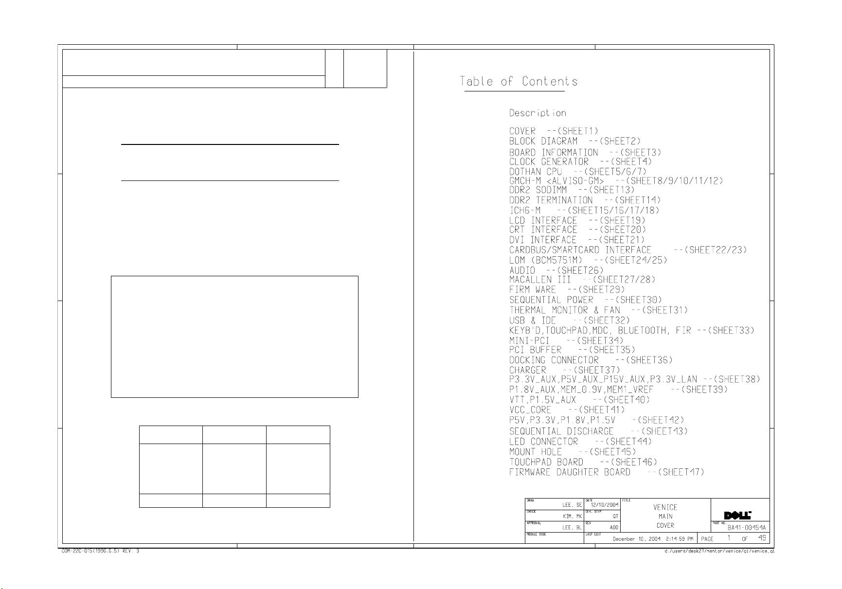
1.
2.
3.
4.
5.
6.
8.
9.
10.
11.
12.
13.
13.
14.
15.
16.
17.
18.
19.
20.
21.
22.
23.
24.
25.
26.
27.
28.
29.
30.
31.
27.
28.
29.
30.
D
C
B
A
SAMSUNG
4
3
2
1
Page 2
This Sheet of Engineering drawings and specifications contains Confidential,
Trade Secret and other Proprietary information of Dell Computer Corporation ( "Dell" ).
This document may not be transferred or copied without the express written authorization of Dell.
In addition, neither this sheet nor the information it contains may be used by or
disclosed to any third party without Dell’s express written consent.
This drawing is property of SEC, Use or copy of this drawing without proper permission
of the appropriate technical-document managing department is prohibited
4
3
Rev.
No
2
1
Option
D
Thermistor
EMC6N300
Clock Generator
CY28411ZCT
Dothan
(478 Micro-FCBGA)
LCD Conn.
LVDS 1ch
SWITCH
CRT
D
4*100Mhz or 4*133Mhz
DDR2-Sodimm
sDVO
SIL1362
DVI
TV out
DDR2-Sodimm
DDR2 1ch
533 & 400Mhz
ALVISO
915GM
(1257 PCBGA)
C
Bluetooth
Powered USB
USB2
USB0
DMI*2
Switch
USB5
PCMCIA
Socket
CardBus
PCI6515
PCI
2x USB
HDD
USB3,4
PATA
AC97
B
Audio
STAC9751T
SPDIF
MDC
ICH6-M
(609 BGA)
LPC
SIO(Macallan III)
(256 LBGA)
PCIE
LOM
BCM5751
X-Bus
Jacks
Docking Connector
RJ11
Smartcard
Socket
MiniPCI
PI3L500
USB1
Buffered LPC
2x PS2
C
Docking
Connector
Q-Switch
RJ45
B
Connector
TAA Option
IRDA
A
Keybd
TP
LED
Firm Ware
Firm Ware
Daughter Board
A
Pointing
Stick
3
24
1
SAMSUNG
Page 3
This Sheet of Engineering drawings and specifications contains Confidential,
Trade Secret and other Proprietary information of Dell Computer Corporation ( "Dell" ).
This document may not be transferred or copied without the express written authorization of Dell.
In addition, neither this sheet nor the information it contains may be used by or
disclosed to any third party without Dell’s express written consent.
This drawing is property of SEC, Use or copy of this drawing without proper permission
of the appropriate technical-document managing department is prohibited
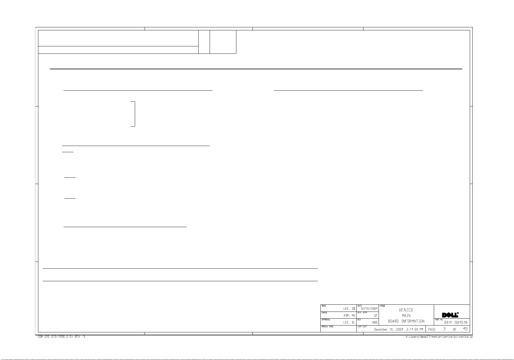
SCHEMATIC ANNOTATIONS AND BOARD INFORMATION
D
4
3
Rev.
No
2
1
D
PCI Devices
Devices
Docking
Cardbus
MiniPCI SLOT
USB
Hub to PCI
LPC bridge/IDE/AC97/SMBUS
AGP
Internal MAC
AC Link
C
B
I2 C / SMB Address
Devices
ICH6
CK-410M (Clock Generator)
SODIMM0
SODIMM1
SSCG
BCM
PWR USB
MAC III
On b’d Diagnostic
Inverter
Battery
Smart Charger
THERMISTER
GMCH
EDID
DVI
USB PORT Assign
PORT NUMBER
0
1
2
3
4
5
6
7
IDSEL#
AD24
AD17
AD19
AD29(internal)
AD30(internal)
AD31(internal)
AD17(internal)
AD24(internal)
-
Address
Master
1101 001x
1010 000x
1010 001X
1101-010x
1100-100x
-
Master
1010 001x
0101 100x
0001 011h
0001 001x
0101 111x
Master
1010 000x
0111 000x
ASSIGNED TO
SYSTEM PORT (Left, Powered USB)
Docking
BLUETOOTH
SYSTEM PORT #1 (Rear)
SYSTEM PORT #2 (Rear)
Expresscard
RFU
RFU
REQ/GNT#
0
1
3
Programable
Hex
-
D2h
A0h
A2h
D4h
C8h
-
-
A2h
58h
16h
12h
5Eh
-
70h
Interrupts
A
D,C
B,D
Bus
SMBUS Master
Clock, Unused Clock Output Disable
-
Spread spectrum Clock Generator
-
-
-
-
-
-
-
I2C Bus
LCD informationA0h
Voltage Rails
VDC
P5V_ALW
P5V_AUX
P3.3V_AUX
P3.3V_LAN
P2.5V_LAN
P1.2V_LAN
P3.3V_ALW
P1.8V_AUX
VCC_CORE
VTT
P5V
P1.5V
P2.5V
P3.3V
MEM_0.9V
Primary DC system power supply (9 to 21V)
5.0V LDO power rail for MAC III(off in S4-S5 without AC Adapter)
5.0V power rail (off in S4-S5)
3.3V power rail (off in S4-S5)
3.3V power rail (off in S4-S5 without AC ADAPTER)
2.5V power rail (off in S4-S5 without AC adapter)
1.25V power rail (off in S4-S5 without AC adapter)
3.3V LDO power rail for MAC III(off in S4-S5 without AC Adapter
GMCH/DDR II Power Source(off in S4-S5)
Core voltage for DOTHAN CPU (0.74~1.30V)
GMCH core, CPU/GMCH FSB Termination.
5.0V switched power rail (off in S3-S5)
1.5V switched power rail (off in S3-S5)
1.8V switched power rail (off in S3-S5)
2.5V switched power rail (off in S3-S5)
3.3V switched power rail (off in S3-S5)
DDR2 Termination (off in S3-S5)
SIL1362(DVI)P1.8V
C
B
A
POWER
P3.3V_LAN
P5V_ALW
P3.3V_ALW MEM_VREF
MAC III
ICH6-M
Flash Memory
Thermistor
P2.5V_LAN
P1.2V_LAN
BCM5751M
LED
4
P5V_AUX
ICH6
USB
STAC9751
P3.3V_AUX
ICH6
MINI-PCI
THERMISTOR
P1.8V_AUX
G MCH
SODIMM
P1.5V_AUX
ICH6
Memory
P5V
ICH4
PCI6515
MINI-PCI
STAC9751
MDC
MAC III
HDD
TOUCHPAD
PCI BUFFER
3
P3.3V
ICH6
PCI6515
MINI-PCI
STAC9751
SODIMM
MAC III
LED
MDC
HDD
FIR
CLOCK
BLUETOOTH
P2.5V
GMCH
ICH
DVI
P1.8V
DVI
P1.5V
MGM
ICH6
MEM_0.9
Memory
VTT
CPU
GMCH
VCC_CORE
CPU
2
A
SAMSUNG
1
Page 4
This Sheet of Engineering drawings and specifications contains Confidential,
Trade Secret and other Proprietary information of Dell Computer Corporation ( "Dell" ).
This document may not be transferred or copied without the express written authorization of Dell.
In addition, neither this sheet nor the information it contains may be used by or
disclosed to any third party without Dell’s express written consent.
This drawing is property of SEC, Use or copy of this drawing without proper permission
of the appropriate technical-document managing department is prohibited
3
Rev.
No
24
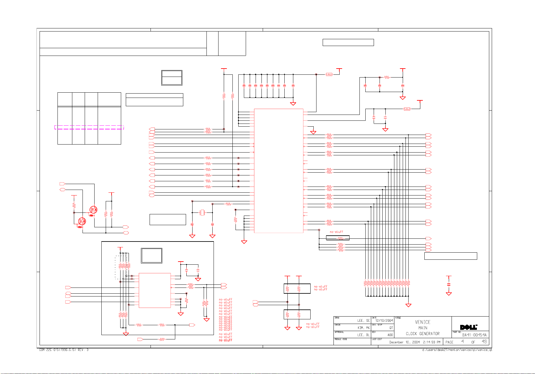
2 Chips solution are propsed by ICS.
CY28411ZXCT : Lead free version
1
D
FSA
BSEL0
CPU
C
SMB3_CLK
SMB3_DATA
Q27
RHU002N06
Q25
RHU002N06
B
CLK3_SSCIN
CLK3_SMBDATA
CLK3_SMBCLK
CLK3_PWRGD*
A
Place SSCG close to ALVISO.
in order to minize the stub.
FSB
00
0
0
0
1
0
1
1
0
0
1
1
1
1
18-B316-D2
48-B424-B4
16-D218-B3 24-B448-B3
P5V
R823
10K
D
3
G
1
S
2
48-C34-B1
4-B3 13-B413-B24-B4
FSC
BSEL2BSEL1
G
1
4
0
1
0
1
0
1
0
1
D
3
S
2
48-C2 4-A44-B313-B213-B4
49-C3 4-A44-B313-B213-B4
49-C34-B4 13-B2 13-B44-B3
48-C2
41-B431-A427-C3
HOST CLK
266 MHz
333 MHz
200 MHz
400 MHz
133 MHz
100 MHz
166 MHz
RSVD1
P3.3V
10K
10K
R223
R219
No Stuff
48-C24-C3
Bus Selection for CK-410M (133MHz)
FSB/FSC : by CPU/ MCH BSEL(Page 6)
FSA : P3.3V PU
CLK3_CB48
CLK3_USB48
CLK3_BSEL1
CLK3_BSEL2
CHP3_PCISTP*
CHP3_CPUSTP*
CLK3_PWRGD*
CLK3_PCLKCB
CLK3_PCLKSIO
CLK3_PCLKDOCK
CLK3_PCLKMIN
CLK3_PCLKICH6M
CLK3_PCLKBCM
CLK3_SMBCLK
CLK3_SMBDATA
CLK3_SMBCLK
CLK3_SMBDATA
P3.3V
SSCD
MK1493-05
10K
R607
R608
CY25823ZC
U9
CY25823ZC
2
S3
3
S2
4
S1
1
CLK_IN
8
SDATA
7
SCLK
5
PWRDWN
6
REFOUT_SEL
33
1%
10K
R603
10K
R602
10K
R604
10K
R605
10K
R65
10K
R66
CLK3_AUD14_1
CK-410M
ICS954201
CY28411ZC
48-C422-B2
48-C3
16-A3
16-B2
4-A3 9-A46-C4
4-A3 9-A46-C4
49-A416-C2
16-C2 41-C449-A46-C4
22-B4 48-C2
28-C3 49-D3
36-B4 49-B3
34-C4
49-C216-C3
24-B4 49-D3
Place 14.318MHz within
500mils of CK-410M
VDDA
VDD
CLK_OUT
CLK_OUT*
IREF
VSSIREF
VSS
VSSA
0
R647
0
R648
49-D34-B1
1%
49.9
R817
R221
C823
4700nF
6.3V
4700nF
1%
1%
49.9
49.9
R229
R818
2.2
C265
6.3V
1%
49.9
R228
1%
49.9
R809
1%
49.9
R808
P3.3V
1%
49.9
R811
C796
1000nF
6.3V
P3.3V
MMZ1608S121AT
B524
49-D3 4-A4
16-B248-C3 16-A3
1%
1%
1%
49.9
49.9
49.9
R810
R224
R225
CLK0_HCLK0
6-C3
CLK0_HCLK0*
6-C3
CLK0_HCLK1
8-B2
CLK0_HCLK1*
8-B2
CLK0_ITP
7-B4
CLK0_ITP*
7-B4
CLK1_MCH3GPLL
9-D4
CLK1_MCH3GPLL*
9-D4
CLK1_PCIEICH
16-B1
CLK1_PCIEICH*
16-B1
CLK1_PCIELAN
24-C4
CLK1_PCIELAN*
24-C4
CLK1_DOTCLK
9-A1
CLK1_DOTCLK*
9-A1
CLK1_DREFCLK
9-A2
CLK1_DREFCLK*
9-A2
CLK3_SSCIN
4-A448-C3
CLK3_AUD14_1
CLK3_ICH14
CLK3_SIO14
28-B348-C3
Place Termination close to CK-410M
P3.3V
C598
47nF
25V
1
D
C
B
A
SAMSUNG
R806
R805
R803
R802
R804
R807
R822
R821
R820
R819
R801
R800
R794
R795
R799
R796
P3.3V
MMZ1608S121AT
B525
33
33
33
33
33
33
33
33
33
33
33
33
33
33
33
33
5.1
R748
5.1
R747
5.1
R746
5.1
R745
100nF
16V
C260
100nF
16V
C825
1%
1%
1%
1%
1%
1%
1%
1%
1%
1%
1%
1%
1%
1%
1%
1%
1%
1%
1%
1%
P3.3V
10K
10K
R737
R791
10
R790
10
R797
5%
48-C24-A4 41-B431-A427-C3
R740
R739
R741
R744
R798
R738
48-C24-A4 13-B413-B24-B4
49-C34-B4 13-B213-B44-A4
1
0.033nF
Y503
C800
14.31818MHz
1%
33
1%
33
1%
33
1%
33
1%
33
1%
33
0
R743
2
0.033nF
C799
475
R222
1%
25V47nF
C824
25V
47nF
C264
6.3V1000nF
16V10nF
C798
C832
U523
CY28411ZXCT
21
VDD_SRC0
28
VDD_SRC1
34
VDD_SRC2
1
VDD_PCI0
7
VDD_PCI1
42
VDD_CPU
12
FSA_USB48
16
FSB_TESTMODE
53
FSC_TESTSEL
55
PCI_STOP*
54
CPU_STOP*
10
VTT_PWRGD*_PD
5
PCI5
PCI4
3
PCI3
56
PCI2
9
PCIF1
8
PCIF0_ITPEN
46
SCLK
47
SDATA
50
XTAL_IN
49
XTAL_OUT
39
IREF
13
VSS_48
29
VSS_SRC
45
VSS_CPU
2
VSS_PCI0
6
VSS_PCI1
51
VSS_REF
25V
47nF
C261
25V47nF
25V47nF
C834
C262
CPU2_ITP_SRC7
CPU2*_ITP_SRC7*
47nF 25V
C263
10000nF
VDD_REF
VDD_48
VDD_A
VSS_A
CPU1
CPU1*
CPU0
CPU0*
SRC6
SRC6*
SRC5
SRC5*
SRC4
SRC4*
SRC3
SRC3*
SRC2
SRC2*
SRC1
SRC1*
SRC0
SRC0*
DOT96
DOT96*
REF
C833
6.3V
48
11
37
38
41
40
44
43
36
35
33
324
31
30
26
27
24
25
22
23
19
20
17
18
14
15
52
Trace Width *2
SMBUS Address "D2h"
P3.3V
1%
1%
1%
1%
1%
49.9
R789
49.9
R788
49.9
R787
49.9
R786
1%
49.9
R793
49.9
R792
C600
C599
10000nF
100nF
16
9
12
R637
11
R636
14
13
10
15
6.3V
1%33
33 1%
1%
1%
1%
475
49.9
49.9
R609
R635
R638
CLK3_AUD14
26-B448-C3
9-A2 9-A1
9-A19-A2
CLK1_DREFSSCLK
CLK1_DREFSSCLK*
CLK3_BSEL1
CLK3_BSEL2
3
VTT
VTT
R49
R50
10K
10K
9-A46-C44-C3
9-A46-C44-C3
R47
R52
0
0
2
Page 5
This Sheet of Engineering drawings and specifications contains Confidential,
Trade Secret and other Proprietary information of Dell Computer Corporation ( "Dell" ).
This document may not be transferred or copied without the express written authorization of Dell.
In addition, neither this sheet nor the information it contains may be used by or
disclosed to any third party without Dell’s express written consent.
This drawing is property of SEC, Use or copy of this drawing without proper permission
of the appropriate technical-document managing department is prohibited
4
3
2
1
Rev.
No
D
VTT
47
C25
E23
B23
C26
E24
D24
B24
C20
B20
A21
B26
A24
B21
A22
A25
A19
D25
C23
C22
K25
N25
H26
M25
N24
L26
M23
G24
F25
H24
M26
L23
G25
H23
K24
L24
J25
J23
J26
CPU500-2
D15*
D14*
D13*
D12*
D11*
D10*
D9*
D8*
D7*
D6*
D5*
D4*
D3*
D2*
D1*
D0*
DINV0*
DSTBN0*
DSTBP0*
D31*
D30*
D29*
D28*
D27*
D26*
D25*
D24*
D23*
D22*
D21*
D20*
D19*
D18*
D17*
D16*
DINV1*
DSTBN1*
DSTBP1*
D47*
D46*
D45*
D44*
D43*
D42*
D41*
D40*
D39*
D38*
DATA GRP 2
D37*
DATA GRP 0DATA GRP 1
D36*
D35*
D34*
D33*
D32*
DINV2*
DSTBN2*
DSTBP2*
D63*
D62*
D61*
D60*
D59*
D58*
D57*
D56*
D55*
D54*
DATA GRP 3
D53*
D52*
D51*
D50*
D49*
D48*
DINV3*
DSTBN3*
DSTBP3*
Y25
AA26
Y23
V26
U25
V24
U26
AA23
R23
R26
R24
V23
U23
T25
AA24
Y26
T24
W25
W24
AF26
AF22
AF25
AD21
AE21
AF20
AD24
AF23
AE22
AD23
AC25
AC22
AC20
AB24
AC23
AB25
AD20
AE24
AE25
CPU1_D*(47:32)CPU1_D*(15:0)
48-B3
48-B3 8-B2
8-D3
8-B2
8-B2
8-B2
8-D3
8-B2
8-B2
CPU1_DBI2*
CPU1_DSTBN2*
CPU1_DSTBP2*
CPU1_D*(63:48)
CPU1_DBI3*
CPU1_DSTBN3*
CPU1_DSTBP3*CPU1_DSTBP1*
47
46
45
44
43
42
419
40
39
38
37
36
35
34
33
32
63
62
61
60
59
58
57
56
55
54
53
52
51
50
49
48
CPU500-1
CPU1_A*(16:3)
CPU1_ADSTB0*
C C
CPU1_REQ*(4:0)
CPU1_A*(31:17)
CPU1_ADSTB1*
8-D2
8-C2
8-B2
8-D2
8-C2
16
15
14
13
12
11
10
9
8
7
6
5
4
3
4
3
2
1
0
31
30
29
28
27
26
25
24
23
22
21
20
19
18
17
1 / 4 2 / 4
AA2
AA3
AF1
AE1
AF3
AD6
AE2
AD5
AC6
AB4
AD2
AE4
AD3
AC3
AC7
AC4
AF4
AE5
A16*
Y3
A15*
A14*
U1
A13*
Y1
A12*
Y4
A11*
W2
A10*
T4
A9*
W1
A8*
V2
A7*
R3
A6*
V3
A5*
U4
A4*
P4
A3*
U3
ADSTB0*
T1
REQ4*
P1
REQ3*
T2
REQ2*
P3
REQ1*
R2
REQ0*
A31*
A30*
A29*
A28*
A27*
A26*
A25*
A24*
A23*
A22*
A21*
A20*
A19*
A18*
A17*
ADSTB1*
BPRI*
DBSY*
DEFER*
DRDY*
ADDR GROUP 0
HITM*
IERR*
LOCK*
TRDY*
RESET*
A20M*
FERR*
IGNNE*
LINT0
ADDR GROUP 1
LINT1
LEGENCY CPU
STPCLK*
ADS*
BNR*
BR0*
DBR*
HIT*
INIT*
RS2*
RS1*
RS0*
SMI*
R48
N2
L1
J3
N4
A7
M2
L4
H2
K3
K4
A4
B5
J2
M3
B11
L2
K1
H1
C2
D3
A3
D1
D4
B4
C6
48-C4 8-A2
48-C4 8-A2
48-C4 8-A2
48-C3 15-C2
48-B3 15-C1
49-D3 15-C2
48-C4 15-C2
48-B4 15-B2
48-C4 15-B2
49-C3 15-B2
48-C4 8-C2
48-C4 8-C2
48-C3 8-C2
48-B3
49-D3 8-B2
48-B3 8-B2
48-C4 8-B2
48-B3 8-B2
48-B315-C2
48-B3 8-B2
48-B3 8-A2
8-C248-B3
7-A330-B2
8-B2
7-A38-C2
CPU1_ADS*
CPU1_BNR*
CPU1_BPRI*
CPU1_BREQ*
ITP3_DBRESET*
CPU1_DBSY*
CPU1_DEFER*
CPU1_DRDY*
CPU1_HIT*
CPU1_HITM*
CPU1_INIT*
CPU1_LOCK*
CPU1_TRDY*
CPU1_CPURST*
CPU1_RS2*
CPU1_RS1*
CPU1_RS0*
CPU1_A20M*
CPU1_FERR*
CPU1_IGNNE*
CPU1_INTR
CPU1_NMI
CPU1_SMI*
CPU1_STPCLK*
CPU1_DBI0*
CPU1_DSTBN0*
CPU1_DSTBP0*
CPU1_D*(31:16)
CPU1_DBI1*
CPU1_DSTBN1*
8-D3
8-B2
8-B2
8-D3
8-B2
8-B2
15
14
13
12
11
10
8
7
6
5
4
3
2
1
0
48-B38-B2
31
30
29
28
27
26
25
24
23
22
21
20
19
18
17
16
48-B38-B2
B B
D
A
A
SAMSUNG
34 2
1
Page 6
This Sheet of Engineering drawings and specifications contains Confidential,
Trade Secret and other Proprietary information of Dell Computer Corporation ( "Dell" ).
This document may not be transferred or copied without the express written authorization of Dell.
In addition, neither this sheet nor the information it contains may be used by or
disclosed to any third party without Dell’s express written consent.
This drawing is property of SEC, Use or copy of this drawing without proper permission
of the appropriate technical-document managing department is prohibited
4
3
2
1
Rev.
No
D
D
P3.3V_ALW
VTT
CPU500-3
3 / 4
48-C415-C28-A2
27.4
54.9 1%
1%54.9
R186
B15
BCLK0
B14
BCLK1
A16
ITP_CLK0
A15
ITP_CLK1
A6
SLP*
B7
DPSLP*
G1
DPRSTP*
C19
DPWR*
E4
PWRGOOD
5
H4
VID5
4
G4
VID4
3
G3
VID3
2
F3
VID2
1
F2
VID1
0
E2
VID0
B17
PROCHOT*
B18
THERMDA
A18
THERMDC
C17
THERMTRIP*
C14
BSEL1
C16
BSEL0
E1
0
PSI*
AD26
GTLREF0
AB1
1%54.9
COMP3
AB2
1%
COMP2
P26
COMP1
P25
1%27.4
COMP0
AE7
VCCSENSE
AF6
VSSSENSE
B2
NC1_RSVD1
C3
RSVD2
AF7
RSVD3
AC1
RSVD4
E26
RSVD5
C5
TEST1
F23
TEST2
HCLKPWR MGMTVIDTHERMMISC
CLK0_HCLK0
CLK0_HCLK0*
VTT
CPU1_SLP*
R81
CPU1_DPSLP*
200
CPU1_DPRSTP*
1%
CPU1_PWRGDCPU
15-C2
CPU1_DPWR*
CPU1_VID(5:0)
C
CPU1_PROCHOT*
CPU2_THERMDA
CPU2_THERMDC
0.5" max length
C224
100nF
CPU1_THRMTRIP*
CLK3_BSEL1
CLK3_BSEL2
CHP3_CPUSTP*
VTT
R164
1K
1%
R187
2K
1%
GTLREF : Keep the Voltage divider within 0.5"
of the first GTLREF0 pin with Zo=55ohm trace.
B
A
Minimize coupling of any switching signals to this net.
COMP0,2(COMP1,3) should be connected with Zo=27.4ohm(55ohm)
trace shorter than 1/2" to their respective Banias socket pins.
GND test points within 100mil of the VCC/VSSsense at the end of the line.
Route the VCC/VSSsense as a Zo=55ohm traces with equal length.
Observe 3:1 spacing b/w VCC/VSSsense lines and 25mil away
(preferred 50mil) from any other signal. And GND via 100mil away
from each of the VCC/VSS test point vias.
Std Voltage Dothan with 533 Mhz FSB updates
VCC (High Frequency Mode) = 1.26 V - 1.356 V (VID values)
TDP (Highest Frequency Mode) =27W (no change)
VCC (Lowest Frequency Mode) = 0.988 V (VID value)
TDP (Lowest Frequency Mode ) = 13.8 W
6-C2 49-B3
49-C331-C2
49-C331-D2
49-C231-C4
4-A3 4-C3 9-A4
49-A4
9-A44-C34-A3
41-C416-C24-C3
4-C1
4-C1
49-D315-C2
15-C2 49-C3
48-B38-B2
41-C4
49-D3
R689
R688
R660
R661
R80
1%
54.9
R185
VCCA3
VCCA2
VCCA1
VCCAVCCPXDP/ITP
VCCA0
VCCP1
VCCP2
VCCP3
VCCP4
VCCP5
VCCP6
VCCP7
VCCP8
VCCP9
VCCP10
VCCP11
VCCP12
VCCP13
VCCP14
VCCP15
VCCP16
VCCP17
VCCP18
VCCP19
VCCP20
VCCP21
VCCP22
VCCP23
VCCP24
VCCP25
VCCQ1
VCCQ0
PREQ*
PRDY*
BPM3*
BPM2*
BPM1*
BPM0*
TRST*
TDO
TMS
TCK
AC26
N1
B1
F26
D10
D12
D14
D16
E11
E13
E15
F10
F12
F14
F16
K6
L5
L21
M6
M22
N5
N21
P6
P22
R5
R21
T6
T22
U21
W4
P23
B10
A10
C9
A9
B8
C8
A13
7-B4 7-B3
C12
TDI
A12
C11
B13
VTT
7-B4
7-B4
7-B4
7-B4
7-B4
7-B4
7-B3
7-B3
7-B3
7-B3
ITP I/F Signal
P1.5V
C644
C643
10000nF
100nF
6.3V
One 0.1uF & 10uF cap for each VCCA pin.
CPU1_PREQ*
CPU1_PRDY*
CPU1_BPM3*
CPU1_BPM2*
CPU1_BPM1*
CPU1_BPM0*
CPU1_TCK
CPU1_TDI
CPU1_TDO
CPU1_TMS
CPU1_TRST*
R51
54.9
1%
CPU1_PROCHOT*
R53
49-B36-C4
1%
CPU Core Voltage Table
VID(5:0)
0
0
0
0
0
0
0
0
0
0
0
0
0
0
0
0
0
1
0
0
0
1
0
1
0
0
0
-
0
0
0
1
0
1
0
0
0
0
0
0
0
0
1
0
1
0
0
0
1
0
1
1
1
0
0
1
0
0
1
0
0
1
1
0
0
1
0
0
00
1
0
0
01
1
0
1
0
0
1
0
1
0
1
1
0
0
0
0
1
0
1
0
1
1
1
0
1
0
1
1
0
0
1
1
0
0
0
1
0
1
0
1
1
1
1
1
1
0
1
1
0
1
11
0
1
1
HFM Voltage
770 : 1.26V ~ 1.372V
730,740,750,760 : 1.26 ~ 1.356
In case of Deeper sheep, core voltage is 0.726V.
Voltage
0
0
1.708 V
0
1.692 V
1
1.676 V
0
1
1.660 V
1
1
0
1.644 V
0
1
1.628 V
1
1.612 V
0
1
1.596 V
1
1
0
0
1.580 V
0
1.564 V
1
0
1
1.548 V
1
1.532 V
1
1.516 V
00
0
1.500 V
0
1
1
0
1.484 V
1
1.468 V
1
0
1.452 V
0
0
1
1.436 V
1
1.420 V
0
1
1.404 V
1
1.388 V
0
0
1
1.372 V
111
1.356 V
0
1
1
1
1
1.340 V
0
1.324 V
0
1.308 V
0
1
1.292 V
0
1
1.276 V
1
1
0
0
1.260 V
0
1.244 V
1
0
1.228 V
1
1
1.212 V
1
P3.3V
R552
1.5K
1%
3
1
475
2
1
Q508
MMBT3904LT1G
3
2
VID(5:0)
0
1
0
0
0
0
0
1
0
1
0
0
1
0
1
0
1
0
0
0
1
0
-
1
01
1
0
1
1
0
1
01
1
0
1
101
0
1
1
1
1
1
0
1
1
0
1
1
1
1
1
000
1
0
1
1
0
1
1
0
1
10
0
1
1
0
1
0
1
1
0
1
1
1
11
1
1
1
1
1
1
1
1
1
1
1
1
1
1
1
1
1
1
1
1
0
0
1
0
0
0
1
1
1
0
0
1
00
1
0
1
1
1
0
1
1
1
1
1
0
0
0
0
0
0
0
0
1
1
1
0
0
1
1
0
1
1
0
1
10
1
0
0
0
1
0
0
1
1
0
1
1
0
0
1
1
0
1
0
1
1
1
1
1
1
0
0
0
0
1
0
0
1
0
1
0
1
1
0
0
0
1
1
11
0
1
1
11
R551
10K
28-B349-A3
Q510
MMBT3904LT1G
Voltage
1.196 V
1.180 V0
1.164 V
1.148 V
1.132 V
1.116 V
1.100 V
1.084 V
1.068 V
1.052 V
1.036 V
1.020 V
1.004 V
0.988 V
0.972 V
0.956 V
0.940 V
0.924 V
0.908 V
0.892 V
0.876 V
0.860 V
0.844 V
0.828 V
0.812 V
0.796 V
0.780 V
0.764 V
0.748 V
0.732 V
0.716 V
0.700 V
KBC3_PROCHOT*
LFM
C
B
A
SAMSUNG
4
3
2
1
Page 7
This Sheet of Engineering drawings and specifications contains Confidential,
Trade Secret and other Proprietary information of Dell Computer Corporation ( "Dell" ).
This document may not be transferred or copied without the express written authorization of Dell.
In addition, neither this sheet nor the information it contains may be used by or
disclosed to any third party without Dell’s express written consent.
This drawing is property of SEC, Use or copy of this drawing without proper permission
of the appropriate technical-document managing department is prohibited
4
3
2
1
Rev.
No
D
AF19
AF21
AE14
AE16
AE18
AE20
AE23
AE26
AF2
AF5
VSS179
VSS147
AB19
AB21
VSS180
VSS181
VSS148
VSS149
AB26
AB23
VSS182
VSS183
VCC37
VCC38
VCC39
VCC40
VCC41
VCC42
VCC43
VCC44
VCC45
VCC46
VCC47
VCC48
VCC49
VCC50
VCC51
VCC52
VCC53
VCC54
VCC55
VCC56
VCC57
VCC58
VCC59
VCC60
VCC61
VCC62
VCC63
VCC64
VCC65
VCC66
VCC67
VCC68
VCC69
VCC70
VCC71
VCC72
VSS150
VSS151
AC2
AF9
VSS184
VSS152
AC5
AC8
VSS185
VSS153
AD15
AD17
AD19
AD22
AD25
AE3
AE6
AE8
AE10
VSS169
VSS170
VSS137
VSS138
AB3
AA25
VSS171
VSS172
VSS140
VSS139
AB5
AB7
VSS173
VSS174
VSS141
VSS142
AB9
AB11
AE12
VSS175
VSS176
VSS143
VSS144
AB13
AB15
VSS177
VSS178
VSS145
VSS146
AB17
AD1
AD4
AD7
AD9
AD11
VSS161
VSS162
VSS163
VCC_CORE
VSS129
VSS130
VSS131
AA6
AA8
AA10
AA12
AD13
VSS164
VSS165
D6
D8
D18
D20
D22
E5
E7
E9
E17
E19
E21
F6
F8
F18
F20
F22
G5
G21
H6
H22
J21
K22
U5
V6
V22
W5
W21
Y6
Y22
AA5
AA7
AA9
AA11
AA13
AA15
VSS132
VSS133
AA14
AA16
VSS166
J5
VSS134
AA18
VSS167
VSS135
VSS168
CPU500-4
4 / 4
VCC1
VCC2
VCC3
VCC4
VCC5
VCC6
VCC7
VCC8
VCC9
VCC10
VCC11
VCC12
VCC13
VCC14
VCC15
VCC16
VCC17
VCC18
VCC19
VCC20
VCC21
VCC22
VCC23
VCC24
VCC25
VCC26
VCC27
VCC28
VCC29
VCC30
VCC31
VCC32
VCC33
VCC34
VCC35
VCC36
VSS136
AA20
AA22
VCC_CORE
C174
10000nF
4V
C740
C218
10000nF
4V
C175
10000nF
4V 4V
C222
10000nF 10000nF
10000nF
4V
4V
C128
C173
10000nF
10000nF
4V
4V
C219
10000nF
4V
C127
10000nF
4V
C89
10000nF
4V
C171
10000nF
4V
C212
4V
C742
10000nF
4V
C214
10000nF
4V
C220
10000nF
4V
C84
10000nF
4V
C123
10000nF
4V
C81
10000nF
4V
C176
10000nF
4V
C217
10000nF
4V
C223
10000nF
4V
C82
10000nF
4V
C129
10000nF
4V
C216
10000nF
4V
C122
10000nF
4V
C126 C213
10000nF
4V
C221
10000nF
4V
C124
10000nF
4V
C177
10000nF
4V
C215
10000nF
4V
C88
10000nF
4V
C172
10000nF
4V
C86
10000nF
10000nF
4V
C90
10000nF
4V
C
VTT
C125
330uF
2.5V
AL
B
CPU1_PREQ*
CPU1_PRDY*
CPU1_BPM3*
CPU1_BPM2*
CPU1_BPM1*
CPU1_BPM0*
CLK0_ITP
CLK0_ITP*
CPU1_TCK
C83
100nF
C132
100nF
6-B3
6-B3
6-B3
6-B3
6-B3
6-B3
4-C1
4-C1
7-B36-B3
C120
100nF
C121
100nF
J520
CONN-28P-FPC
13
BPM5*
15
BPM4*
17
BPM3*
19
BPM2*
21
BPM1*
23
BPM0*
9
BCLK
8
BCLK*
11
FBO
10
GND1
14
GND2
16
GND3
18
GND4
20
GND5
22
GND6
C85
100nF
VTT1
VTT2
VTAP
TDO
TMS
TRST*
RESET*
DBR*
DBA*
TCK
NC1
NC2
C131
C130
100nF
100nF
C87
100nF
VTT
27
28
26
5
1
TDI
7
2
3
12
25
24
4
6
R588
R29
100nF16V
C596
C118
100nF
C119
100nF
P3.3V_AUX
1%
150
R46
22.6
1%
22.6
1%
VTT
1%
40.2
R30
1%
27.4
VTT
1%
1%
150
54.9
54.9
near the CPU
R590
R587
R589
CPU1_TCK
6-B37-B4
CPU1_TDI
6-B3
CPU1_TDO
6-B3
CPU1_TMS
6-B3
CPU1_TRST*
6-B3
CPU1_CPURST*
5-C38-C2
ITP3_DBRESET*
30-B2 5-C3
475
A2
VSS1
A5
VSS2
A8
VSS3
A11
VSS4
A14
VSS5
A17
VSS6
A20
VSS7
A23
VSS8
A26
VSS9
B3
VSS10
B6
VSS11
B9
VSS12
B12
VSS13
B16
VSS14
B19
VSS15
B22
VSS16
B25
VSS17
C1
VSS18
C4
VSS19
C7
VSS20
C10
VSS21
C13
VSS22
C15
VSS23
C18
VSS24
C21
VSS25
C24
VSS26
D2
VSS27
D5
VSS28
D7
VSS29
D9
VSS30
D11
VSS31
D13
VSS32
D15
VSS33
D17
VSS34
D19
VSS35
D21
VSS36
D23
VSS37
D26
VSS38
E3
VSS39
E6
VSS40
E8
VSS41
E10
VSS42
E12
VSS43
E14
VSS44
E16
VSS45
E18
VSS46
E20
VSS47
E22
VSS48
E25
VSS49
F1
VSS50
F4
VSS51
F5
VSS52
F7
VSS53
F9
VSS54
F11
VSS55
F13
VSS56
F15
VSS57
F17
VSS58
F19
VSS59
F21
VSS60
F24
VSS61
G2
VSS62
G6
VSS63
G22
VSS64
AF11
AF13
AF15
VSS186
VSS187
VSS188
VCC_CORE
AA17
AA19
AA21
AB6
AB8
AB10
AB12
AB14
AB16
AB18
AB20
AB22
AC9
AC11
AC13
AC15
AC17
AC19
AD8
AD10
AD12
AD14
AD16
AD18
AE9
AE11
AE13
AE15
AE17
AE19
AF8
AF10
AF12
AF14
AF16
AF18
VSS154
VSS155
VSS156
AC10
AC12
AC14
AF17
VSS189
VSS157
AC18
AC16
AF24
VSS190
VSS191
VSS158
VSS159
AC21
AC24
VSS192
VSS160
VSS65
VSS66
VSS67
VSS68
VSS69
VSS70
VSS71
VSS72
VSS73
VSS74
VSS75
VSS76
VSS77
VSS78
VSS79
VSS80
VSS81
VSS82
VSS83
VSS84
VSS85
VSS86
VSS87
VSS88
VSS89
VSS90
VSS91
VSS92
VSS93
VSS94
VSS95
VSS96
VSS97
VSS98
VSS99
VSS100
VSS101
VSS102
VSS103
VSS104
VSS105
VSS106
VSS107
VSS108
VSS109
VSS110
VSS111
VSS112
VSS113
VSS114
VSS115
VSS116
VSS117
VSS118
VSS119
VSS120
VSS121
VSS122
VSS123
VSS124
VSS125
VSS126
VSS127
VSS128
G23
G26
H3
H5
H21
H25
J1
J4
J6
J22
J24
K2
K5
K21
K23
K26
L3
L6
L22
L25
M1
M4
M5
M21
M24
N3
N6
N22
N23
N26
P2
P5
P21
P24
R1
R4
R6
R22
R25
T3
T5
T21
T23
T26
U2
U6
U22
U24
V1
V4
V5
V21
V25
W3
W6
W22
W23
W26
Y2
Y5
Y21
Y24
AA1
AA4
D
C
B
J520 connector didn’t place in the board.
R591
R592
AA
SAMSUNG
3
24
1
Page 8
This Sheet of Engineering drawings and specifications contains Confidential,
Trade Secret and other Proprietary information of Dell Computer Corporation ( "Dell" ).
This document may not be transferred or copied without the express written authorization of Dell.
In addition, neither this sheet nor the information it contains may be used by or
disclosed to any third party without Dell’s express written consent.
This drawing is property of SEC, Use or copy of this drawing without proper permission
of the appropriate technical-document managing department is prohibited
4
3
2
1
Rev.
No
R662
24.9
1%
U514-1
915GM(DELL)
1 / 5
E4
HD0*
E1
HD1*
F4
HD2*
H7
HD3*
E2
HD4*
F1
HD5*
E3
HD6*
D3
HD7*
K7
HD8*
F2
HD9*
J7
HD10*
J8
HD11*
H6
HD12*
F3
HD13*
K8
HD14*
H5
HD15*
H1
HD16*
H2
HD17*
K5
HD18*
K6
HD19*
J4
HD20*
G3
HD21*
H3
HD22*
J1
HD23*
L5
HD24*
K4
HD25*
J5
HD26*
P7
HD27*
L7
HD28*
J3
HD29*
P5
HD30*
L3
HD31*
U7
HD32*
V6
HD33*
R6
HD34*
R5
HD35*
P3
HD36*
T8
HD37*
R7
HD38*
R8
HD39*
U8
HD40*
R4
HD41*
T4
HD42*
T5
HD43*
R1
HD44*
T3
HD45*
V8
HD46*
U6
HD47*
W6
HD48*
U3
HD49*
V5
HD50*
W8
HD51*
W7
HD52*
U2
HD53*
U1
HD54*
Y5
HD55*
Y2
HD56*
V4
HD57*
Y7
HD58*
W1
HD59*
W3
HD60*
Y3
HD61*
Y6
HD62*
W2
HD63*
C1
HXRCOMP
C2
HXSCOMP
D1
HXSWING
T1
HYRCOMP
L1
HYSCOMP
P1
HYSWING
R165
24.9
1%
HOST
HA3*
HA4*
HA5*
HA6*
HA7*
HA8*
HA9*
HA10*
HA11*
HA12*
HA13*
HA14*
HA15*
HA16*
HA17*
HA18*
HA19*
HA20*
HA21*
HA22*
HA23*
HA24*
HA25*
HA26*
HA27*
HA28*
HA29*
HA30*
HA31*
HADS*
HADSTB*0
HADSTB*1
HVREF
HBNR*
HBPRI*
HBREQ0*
HCPURST*
HCLKINN
HCLKINP
HDBSY*
HDEFER*
HDINV*0
HDINV*1
HDINV*2
HDINV*3
HDPWR*
HDRDY*
HDSTBN*0
HDSTBN*1
HDSTBN*2
HDSTBN*3
HDSTBP*0
HDSTBP*1
HDSTBP*2
HDSTBP*3
HEDRDY*
HHIT*
HHITM*
HLOCK*
HPCREQ*
HREQ*0
HREQ*1
HREQ*2
HREQ*3
HREQ*4
HRS0*
HRS1*
HRS2*
HCPUSLP*
HTRDY*
CPU1_ADS*
CPU1_ADSTB0*
CPU1_ADSTB1*
CPU1_BNR*
CPU1_BPRI*
CPU1_BREQ*
CPU1_CPURST*
CLK0_HCLK1*
CLK0_HCLK1
CPU1_DBSY*
CPU1_DEFER*
CPU1_DBI0*
CPU1_DBI1*
CPU1_DBI2*
CPU1_DBI3*
CPU1_DPWR*
CPU1_DRDY*
CPU1_DSTBN0*
CPU1_DSTBN1*
CPU1_DSTBN2*
CPU1_DSTBN3*
CPU1_DSTBP0*
CPU1_DSTBP1*
CPU1_DSTBP2*
CPU1_DSTBP3*
CPU1_HIT*
CPU1_HITM*
CPU1_LOCK*
CPU1_REQ*(4:0)
5-C348-C4
5-C3
5-C45-D4
CPU1_RS0*
CPU1_RS1*
CPU1_RS2*
CPU1_SLP*
CPU1_TRDY*
G9
C9
E9
B7
A10
F9
D8
B10
E10
G10
D9
E11
F10
G11
G13
C10
C11
D11
C12
B13
A12
F12
G12
E12
C13
B11
D13
A13
F13
F8
B9
E13
J11
A5
D5
E7
H10
AB1
AB2
C6
E6
H8
K3
T7
U5
G6
F7
G4
K1
R3
V3
G5
K2
R2
W4
F6
D4
D6
B3
A11
A7
D7
B8
C7
A8
A4
C5
B4
G8
R82
B5
3
4
5
6
7
8
9
10
11
12
13
14
15
16
17
18
19
20
21
22
23
24
25
26
27
28
29
30
31
48-C4 5-D3
5-C4
5-B4
48-C4 5-C3
48-C3 5-C3
48-B3 5-C3
7-A3 5-C3
4-C1
4-C1
48-B3 5-C3
48-B3
5-C3
5-C2
49-D3
5-B248-B3
48-B3 5-C1
48-B3 5-B1
48-B3 6-C3
5-C3
48-B3
5-C2
5-B2
5-C1
5-B1
5-C2
5-B2
5-C1
5-B1
5-C3
48-C4
5-C348-B3
48-B3 5-C3
5-C4
0
1
2
3
4
48-C4 5-C3
48-C4 5-C3
0
48-C4 15-C2 6-C3
48-B3
CPUSLP
Dothan A stepping : Stuff resistor on SLP* of ICH6-M
Dothan B stepping : Stuff resistor on SLP* of GMCH.
CPU1_A*(31:3)
VTT
R112
100
1%
0.7V
R111
C133
200
100nF
1608
1%
Placed as close as possible.
D
C
B
A
D
CPU1_D*(63:0)
C
VTT
R663
221
1%
R664
100
1%
C693
100nF
Trace should be 10-mil wide
with 20mil spacing.
49-B3 8-A3
0.327V
MCH1_HXSWING
VTT
Trace should be 10-mil wide
C727
100nF
49-B3 8-A3
with 20mil spacing.
MCH1_HYSWING
0.327V
MCH1_HXSWING
MCH1_HYSWING
Trace should be 10-mil wide
with 20mil spacing.
R692
221
B
1%
R690
100
1%
5-C1 5-C2 5-D1 5-D2
VTT
R691
54.9
1%
8-C4 49-B3
8-B4 49-B3
R632
54.9
1%
0
1
2
3
4
5
6
7
8
9
10
11
12
13
14
15
16
17
18
19
20
21
22
23
24
25
26
27
28
29
30
31
32
33
34
35
36
37
38
39
40
41
42
43
44
45
46
47
48
49
50
51
52
53
54
55
56
57
58
59
60
61
62
63
A
SAMSUNG
4
3
2
1
Page 9
This Sheet of Engineering drawings and specifications contains Confidential,
Trade Secret and other Proprietary information of Dell Computer Corporation ( "Dell" ).
This document may not be transferred or copied without the express written authorization of Dell.
In addition, neither this sheet nor the information it contains may be used by or
disclosed to any third party without Dell’s express written consent.
This drawing is property of SEC, Use or copy of this drawing without proper permission
of the appropriate technical-document managing department is prohibited
A
B
TV DAC
Component
D
C
Place 75 ohm termination resistors
close to GMCH
C
VGA3_BLUE_INT
VGA3_GREEN_INT
VGA3_RED_INT
RED, GREEN, BLUE
are GND referenced
B
LCD2_BIAPWM
CFG#
CFG(5)
A
CFG(6)
CFG(7)
CFG(9)
CFG(16)
CFG(19)
SDVODTA
4
Composite
Pb
CVBS
Y
Pr
DVO2_CTRLDATA
DVO2_CTRLCLK
CLK1_MCH3GPLL*
CLK1_MCH3GPLL
TVO3_COMP
TVO3_Y_G
TVO3_C_R
VGA2_DDCCLK
VGA2_DDCDATA
20-A4
20-A2
49-D2
20-A2
20-A4
49-C2
20-A4
20-A2
49-B3
49-C427-C2
Current Setting
Low
DMIx2
DDR-2
DT/Transportable
PEG Reversal
Dynamic ODT
Disabled
VCC 1.05V (def.)
VTT 1.05V (def.)
No (def.)
21-B3 49-C3
4-C1
4-C1
36-B1
20-B4 49-A4
VGA3_VSYNC
1%
VGA3_HSYNC
150 1%
150 1%
255 1%
150
LCD2_BIAPWM
R122
R123
R121
R120
LCD2_BKLTON
LCD2_DDCCLK
LCD2_DDCDATA
LCD2_VDDEN
R127
1.5K
1%
LCD1_CLK*
LCD1_CLK
LCD1_DATA0*
LCD1_DATA1*
LCD1_DATA2*
LCD1_DATA0
LCD1_DATA1
LCD1_DATA2
R126
100K
(def. : default Option)
High
DMIx4 (def.)
DDR-1
Mobile CPU (def.)
Normal
Enabled (def.)
VCC 1.5VCFG(18)
VTT 1.2V
SDVO Present
49-A321-B3
48-B3
48-B436-C2
49-B320-B4
MCH_P1.5V
1%
24.9
R128
H24
H25
AB29
AC29
A15
C16
A17
J18
751%
R117
R116
1% 75
B15
B16
4.99K
B17
R119
R113
1%
1% 75
E24
E23
E21
D21
C20
B20
A19
B19
H21
20-C4 48-B2
G21
48-B220-D4
J20
E25
27-C2
49-C4
F25
19-A349-C4
C23
C22
F23
49-C419-B4
F22
49-B3
19-A4
F26
19-C4
28-B3 13-B214-C3
C33
48-B3
C31
F28
F27
B30
19-B2
B29
19-B2
C25
C24
B34
19-C2
B33
19-C2
B32
19-B2
A34
19-C2
A33
19-C2
B31
19-B2
C29
D28
C27
C28
D27
C26
VTT
CLK3_BSEL1
CLK3_BSEL2
21-C3
D36
D34
E30
F34
EXP_RXN0
EXP_COMPI
EXP_ICOMPO
SDVOCTRL_DATA
SDVOCTRL_CLK
GCLKN
GCLKP
TVDAC_A
Pb
TVDAC_B
Y
TVDAC_C
Pr
TV_REFSET
TV_IRTNA
TV_IRTNB
TV_IRTNC
DDCCLK
DDCDATA
BLUE
BLUE*
GREEN
GREEN*
RED
RED*
VSYNC
HSYNC
REFSET
LBKLT_CRTL
LBKLT_EN
LCTLA_CLK
LCTLB_DATA
LDDC_CLK
LDDC_DATA
LVDD_EN
LIBG
LVBG
LVREFH
LVREFL
LACLKN
LACLKP
LBCLKN
LBCLKP
LADATAN0
LADATAN1
LADATAN2
LADATAP0
LADATAP1
LADATAP2
LBDATAN0
LBDATAN1
LBDATAN2
LBDATAP0
LBDATAP1
LBDATAP2
R115
4-A3
4-C3 6-C4
4-A3 6-C44-C3
G30
H34
J30
K34
EXP_RXN2
EXP_RXN3
EXP_RXN4
EXP_RXN1
MISCTVVGALVDS
G16
10K
CFG(17:3)
CFG(20:18)
DVO3_INT*
P34
L30
M34
N30
EXP_RXN9
EXP_RXN5
EXP_RXN6
EXP_RXN7
EXP_RXN8
CFG2
CFG3
CFG4
CFG0
CFG1
F16
F15
H13
G14
R114
2.21k
1%
Internal Pull-up
Internal Pull-down
U30
R30
T34
EXP_RXN10
EXP_RXN11
EXP_RXN12
CFG5
CFG6
CFG7
E16
D17
G15
R118
2.21k
1%
V34
W30
EXP_RXN13
CFG8
J16
D15
4
3
Rev.
No
21-C3
DVO3_INT
P36
U32
V36
W32
D30
Y34
EXP_RXP0
EXP_RXN14
EXP_RXN15
E34
F30
G34
EXP_RXP1
EXP_RXP2
H30
J34
K30
EXP_RXP4
EXP_RXP5
EXP_RXP3
L34
M30
N34
EXP_RXP6
EXP_RXP7
EXP_RXP8
P30
R34
T30
EXP_RXP9
EXP_RXP10
EXP_RXP11
U34
V30
W34
EXP_RXP12
EXP_RXP13
EXP_RXP14
EXP_RXP15
G32
E32
F36
EXP_TXN0
EXP_TXN1
H36
J32
K36
EXP_TXN2
EXP_TXN3
EXP_TXN4
L32
M36
N32
EXP_TXN5
EXP_TXN6
EXP_TXN7
R32
T36
EXP_TXN9
EXP_TXN8
EXP_TXN10
EXP_TXN13
EXP_TXN14
EXP_TXN11
EXP_TXN12
Y36
PCI-EXPRESS GRAPHICS
U514-2
915GM(DELL)
2 / 5
CFG/RSVD PM CLK NC
EXT_TS0*
EXT_TS1*
DREF_CLKN
DREF_CLKP
DREF_SSCLKN
CFG9
E15
CFG10
CFG11
D14
3
CFG12
E14
CFG13
H12
C14
CFG15
CFG16
CFG17
CFG18
CFG14
J15
H15
H14
G22
G23
MCH2_BMBUSY*
P2.5V
CFG19
CFG20
D23
RSVD21
G25
G24
10K
10K
RSVD22
RSVD23
J17
A31
16-C2 49-B3
RSVD24
RSVD25
A30
D26
R125
R124
RSVD26
RSVD27
D25
BM_BUSY*
J21
J23
THRMTRIP*
F5
H22
AD30
48-B3 16-B227-C330-B3
RSTIN*
PWROK
AE29
48-C3
A24
A23
C37
1%
R192
21-B3 16-B4 16-A2
24-B4
31-A4
DREF_SSCLKP
NC1
NC2
NC3
D37
AP37
AP36
AN37
4-A39-A1
9-A1 4-A3
4-B1
4-B1
100
24-C4
27-D2
49-B2
31-B4
AP2
2
J36
K32
L36
EXP_TXP4
EXP_TXP5
EXP_TXP6
NC10
NC11
A37
100nFC104
100nFC141
100nFC106
100nFC142
M32
N36
P32
EXP_TXP7
EXP_TXP8
EXP_TXP9
EXP_TXP10
DMIDDR MUXING
SM_OCDCOMP0
SM_OCDCOMP1
10V
10V
10V
10V
10V
10V
10V
10V
R36
T32
U36
V32
W36
EXP_TXP11
EXP_TXP12
EXP_TXP13
EXP_TXP14
EXP_TXP15
DMI0RXN
DMI0RXP
DMI0TXN
DMI0TXP
DMI1RXN
DMI1RXP
DMI1TXN
DMI1TXP
DMI2RXN
DMI2RXP
DMI2TXN
DMI2TXP
DMI3RXN
DMI3RXP
DMI3TXN
DMI3TXP
SM_CK0
SM_CK1
SM_CK2
SM_CK3
SM_CK4
SM_CK5
SM_CK0*
SM_CK1*
SM_CK2*
SM_CK3*
SM_CK4*
SM_CK5*
SM_CKE0
SM_CKE1
SM_CKE2
SM_CKE3
SM_CS0*
SM_CS1*
SM_CS2*
SM_CS3*
SM_ODT0
SM_ODT1
SM_ODT2
SM_ODT3
SMRCOMPN
SMRCOMPP
SMVREF0
SMVREF1
SMXSLEWIN
SMXSLEWOUT
SMYSLEWIN
SMYSLEWOUT
AA31
Y31
AA33
Y33
AB35
AA35
AB37
AA37
AC31
AB31
AC33
AB33
AD35
AC35
AD37
AC37
AM33
AL1
AE11
AJ34
AF6
AC10
AN33
AK1
AE10
AJ33
AF5
AD10
AP21
AM21
AH21
AK21
AN16
AM14
AH15
AG16
AF22
AF16
AP14
AL15
AM11
AN10
AK10
AK11
AF37
AD1
AE27
AE28
AF9
AF10
21-B3
21-B3
21-B3
21-C3
21-C3
21-B3
21-B3
21-C3
16-C1
16-C1
16-C1
16-C136-B1 48-B4
16-C1
16-C1
16-C1
16-C1
13-C4
13-B4
13-C2
13-C2
13-C4
13-B4
13-C2
13-B2
13-B414-C3
13-B414-C3
14-C3 13-B2
13-C414-D3
13-C414-D3
14-C3 13-C2
14-C3 13-C2
14-C3 13-B4
14-C3 13-B4
13-B214-C3
13-B214-C3
MEM1_VREF
CLK1_DREFSSCLK
D32
E36
F32
EXP_TXP0
EXP_TXP1
EXP_TXP2
EXP_TXN15
NC4
NC5
NC6
NC7B1NC8A2NC9
AP1
AN1
CLK1_DREFSSCLK
CLK1_DREFSSCLK*
CLK1_DREFCLK
CLK1_DREFCLK*
PLT3_RST*
IMVP_PWRGD
GMCH1_THRMTRIP*
C103 100nF
C139 100nF
C105 100nF
C140 100nF
H32
G36
EXP_TXP3
A36
B37
2 1
DVO3_RED*
DVO3_GREEN*
DVO3_BLUE*
DVO3_CLK*
DVO3_RED
DVO3_GREEN
DVO3_BLUE
DVO3_CLK
DMI1_TXN0
DMI1_TXP0
DMI1_RXN0
DMI1_RXP0
DMI1_TXN1
DMI1_TXP1
DMI1_RXN1
DMI1_RXP1
CLK1_MCLK0
CLK1_MCLK1
CLK1_MCLK3
CLK1_MCLK4
CLK1_MCLK0*
CLK1_MCLK1*
CLK1_MCLK3*
CLK1_MCLK4*
MEM1_CKE0
MEM1_CKE1
MEM1_CKE2
MEM1_CKE3
MEM1_CS0*
MEM1_CS1*
MEM1_CS2*
MEM1_CS3*
P1.8V_AUX
MEM1_ODT0
MEM1_ODT1
MEM1_ODT2
MEM1_ODT3
4-A3 9-A2
1
Route as short as possible
1608
R190
R191
40.2
40.2
1%
1%
R189
80.6
1%
R218
80.6
1%
Place these close to SSCD.
9-A24-A3
R130
R129
0
0
CLK1_DOTCLK
4-B1
CLK1_DOTCLK*CLK1_DREFSSCLK*
4-B1
SAMSUNG
D
C
B
A
Page 10
This Sheet of Engineering drawings and specifications contains Confidential,
Trade Secret and other Proprietary information of Dell Computer Corporation ( "Dell" ).
This document may not be transferred or copied without the express written authorization of Dell.
In addition, neither this sheet nor the information it contains may be used by or
disclosed to any third party without Dell’s express written consent.
This drawing is property of SEC, Use or copy of this drawing without proper permission
of the appropriate technical-document managing department is prohibited
4
Rev.
No
23
1
D
C
B
MEM1_ADQ(63:0)
13-D2 13-D4
MEM1_ABS0*
MEM1_ABS1*
MEM1_ABS2*
MEM1_ADM(7:0)
MEM1_ADQS(7:0)
MEM1_ADQS*(7:0)
MEM1_AMA(13:0)
MEM1_ACAS*
MEM1_ARAS*
MEM1_AWE*
14-C313-C4
14-C313-C4
13-C414-C3
13-B413-B2
13-B2 13-B4
13-A413-A2
14-D413-C4
13-B4 14-C3
14-C313-B4
14-C313-B4
0
1
2
3
4
5
6
7
0
1
2
3
4
5
6
7
0
1
2
3
4
5
6
7
0
1
2
3
4
5
6
7
8
9
10
11
12
13
AK15
AK16
AL21
AJ37
AP35
AL29
AP24
AK36
AP33
AN29
AP23
AK35
AP34
AN30
AN23
AL17
AP17
AP18
AM17
AN18
AM18
AL19
AP20
AM19
AL20
AM16
AN20
AM20
AM15
AN15
AP16
AF29
AF28
AP15
AP9
AP4
AD3
AM8
AM4
AE5
AN8
AM5
AH1
AE4
AJ2
AJ1
2
1
0
3
AG35
AH35
AL37
AL35
SADQ0
SADQ1
SADQ3
SADQ2
SA_BS0*
SA_BS1*
SA_BS2*
SA_DM0
SA_DM1
SA_DM2
SA_DM3
SA_DM4
SA_DM5
SA_DM6
SA_DM7
SA_DQS0
SA_DQS1
SA_DQS2
SA_DQS3
SA_DQS4
SA_DQS5
SA_DQS6
SA_DQS7
SA_DQS0*
SA_DQS1*
SA_DQS2*
SA_DQS3*
SA_DQS4*
SA_DQS5*
SA_DQS6*
SA_DQS7*
SA_MA0
SA_MA1
SA_MA2
SA_MA3
SA_MA4
SA_MA5
SA_MA6
SA_MA7
SA_MA8
SA_MA9
SA_MA10
SA_MA11
SA_MA12
SA_MA13
SA_CAS*
SA_RAS*
SA_RCVENIN*
SA_RCVENOUT*
SA_WE*
8
5
976
4
10
AL34
AM36
AN35
AP32
AK37
AJ35
AH36
SADQ7
SADQ8
SADQ9
SADQ6
SADQ5
SADQ4
DDR SYSTEM MEMORY A
12
11
AM31
AM34
SADQ10
SADQ11
14
13
AM35
AL32
SADQ12
SADQ13
16
15
AM32
AN31
SADQ14
SADQ15
SADQ16
17
18
AP31
AN28
SADQ17
20
19
AP28
AL30
SADQ18
SADQ19
21
22
AM28
AM30
SADQ20
SADQ21
23
AL28
SADQ22
25
24
AP27
AM27
SADQ23
SADQ24
SADQ25
26
AM23
AM22
SADQ26
29
28
AL23
AM24
SADQ27
SADQ28
SADQ29
31
30
AP22
AN22
SADQ30
32
AM9
AL9
SADQ32
SADQ31
33
27
U514-3
915GM(DELL)
3 / 5
35
34
AL6
AP7
SADQ33
SADQ34
36
37
AP11
AP10
SADQ35
SADQ36
39
38
AL7
AM7
SADQ37
SADQ38
40
41
AN6
AN5
SADQ39
SADQ40
42
AN3
SADQ41
51
46
47
AL4
AM3
SADQ46
49
48
AK2
AK3
SADQ47
SADQ48
50
AG1
AG2
SADQ49
SADQ50
52
AL3
SADQ51
43
44
AP3
AP6
SADQ42
SADQ43
45
AM6
SADQ44
SADQ45
DDR SYSTEM MEMORY B
54
53
AM2
AH3
SADQ52
SADQ53
55
56
AG3
AF3
SADQ54
SADQ55
57
58
60
59
AF2
AE3
AD6
AC4
SADQ56
SADQ57
SADQ58
SADQ59
SB_RCVENIN*
SB_RCVENOUT*
61
63
62
AF1
AD4
AD5
SADQ61
SADQ62
SADQ60
SB_BS0*
SB_BS1*
SB_BS2*
SB_DM0
SB_DM1
SB_DM2
SB_DM3
SB_DM4
SB_DM5
SB_DM6
SB_DM7
SB_DQS0
SB_DQS1
SB_DQS2
SB_DQS3
SB_DQS4
SB_DQS5
SB_DQS6
SB_DQS7
SB_DQS0*
SB_DQS1*
SB_DQS2*
SB_DQS3*
SB_DQS4*
SB_DQS5*
SB_DQS6*
SB_DQS7*
SB_MA0
SB_MA1
SB_MA2
SB_MA3
SB_MA4
SB_MA5
SB_MA6
SB_MA7
SB_MA8
SB_MA9
SB_MA10
SB_MA11
SB_MA12
SB_MA13
SB_CAS*
SB_RAS*
SB_WE*
SADQ63
AJ15
AG17
AG21
AF32
AK34
AK27
AK24
AJ10
AK5
AE7
AB7
AF34
AK32
AJ28
AK23
AM10
AH6
AF8
AB4
AF35
AK33
AK28
AJ23
AL10
AH7
AF7
AB5
AH17
AK17
AH18
AJ18
AK18
AJ19
AK19
AH19
AJ20
AH20
AJ16
AG18
AG20
AG15
AH14
AK14
AF15
AF14
AH16
10
11
12
13
0
1
2
3
4
5
6
7
8
9
14-C3 13-C2
13-C214-C3
14-C3 13-C2
14-B3 13-B2
14-B3 13-B2
13-C2
14-B4
13-B214-B3
MEM1_BBS0*
MEM1_BBS1*
MEM1_BBS2*
MEM1_BMA(13:0)
MEM1_BCAS*
MEM1_BRAS*
MEM1_BWE*
DDR/DDR2 Common Signal Mappping
Single Channel Mode Signal Mapping
Single Channel Signal Mapping.
SO-DIMM 0
SM_CK [1:0]
SM_CK* [1:0]
(DDR2 support)
SM_CS* [1:0]
SM_CKE [1:0]
SM_ODT [1:0]
SA_BS [2:0]
SA_DQ [63:0]
SA_DQS [7:0]
SA_DQS* [7:0]
SA_DM [7:0]
SO-DIMM 1
SM_CK [4:3]
SM_CK* [4:3]
(DDR2 support)
SM_CS* [3:2]
SM_CK [3:2]
SM_ODT [3:2]
(DDR2 support)(DDR2 support)
SB_BS [2:0]
SB_MA [13:0]SA_MA [13:0]
SB_RAS*SA_RAS*
SB_CAS*SA_CAS*
SB_WE*SA_WE*
D
C
B
SBDQ0
SBDQ6
SBDQ7
SBDQ8
AE31
SBDQ1
AE32
SBDQ2
AG32
SBDQ3
AG36
SBDQ4
AE33
AE34
SBDQ5
AF31
AF30
AH33
SBDQ9
AH32
SBDQ10
AK31
AG30
SBDQ11
SBDQ12
AG34
AG33
SBDQ13
SBDQ14
AJ31
AH31
SBDQ15
SBDQ16
AJ30
AK30
SBDQ17
SBDQ18
AH28
AH29
SBDQ20
SBDQ19
AK29
AH30
SBDQ21
SBDQ22
AH27
AG28
SBDQ23
SBDQ24
AF24
AG23
SBDQ25
SBDQ26
AJ22
AK22
SBDQ29
SBDQ27
SBDQ28
AH23
AH24
SBDQ30
AJ21
AG22
SBDQ31
SBDQ32
AG9
AG10
SBDQ33
SBDQ34
AH8
AG8
SBDQ35
SBDQ36
AH11
AH10
SBDQ37
SBDQ38
AJ9
AK9
SBDQ39
SBDQ40
AJ7
AK6
SBDQ41
SBDQ42
AJ4
AH5
SBDQ43
SBDQ44
AJ8
AK8
SBDQ45
SBDQ46
AJ5
AK4
SBDQ47
SBDQ48
AG5
AG4
SBDQ49
SBDQ50
AD8
AD9
SBDQ51
AH4
A
SBDQ52
SBDQ53
AE8
AG6
SBDQ54
SBDQ55
AD7
AC5
SBDQ56
SBDQ57
AB6
AB8
SBDQ58
SBDQ59
AA8
AC8
SBDQ60
SBDQ61
SBDQ62
AA4
AC7
SBDQ63
AA5
A
SAMSUNG
4
2
13
Page 11
B523
BLM18PG181SN1
C229
100nF
VCCA_TVBG
VSSA_TVBG
VCCD_TVDAC
VCCDQ_TVDAC
VSSA_CRTDAC
VCC_SYNC
VTT0
VTT1
VTT2
VTT3
VTT4
VTT5
VTT6
VTT7
VTT8
VTT9
VTT10
VTT11
VTT12
VTT13
VTT14
VTT15
VTT16
VTT17
VTT18
VTT19
VTT20
VTT21
VTT22
VTT23
VTT24
VTT25
VTT26
VTT27
VTT28
VTT29
VTT30
VTT31
VTT32
VTT33
VTT34
VTT35
VTT36
VTT37
VTT38
VTT39
VTT40
VTT41
VTT42
VTT43
VTT44
VTT45
VTT46
VTT47
VTT48
VTT49
VTT50
VTT51
VCC3G0
VCC3G1
VCC3G2
VCC3G3
VCC3G4
VCC3G5
VCC3G6
VCCA_3GBG
VSSA_3GBG
2
C746
330uF
2.5V
AL
F17
E17
D18
C18
F18
E18
H18
G18
D19
H17
F19
E19
G19
H20
K13
J13
K12
W11
V11
U11
T11
R11
P11
N11
M11
L11
K11
W10
V10
U10
T10
R10
P10
N10
M10
K10
J10
Y9
W9
U9
R9
P9
N9
M9
L9
J9
N8
M8
N7
M7
N6
M6
A6
N5
M5
N4
M4
N3
M3
N2
M2
B2
V1
N1
M1
G1
AE37
W37
U37
R37
N37
L37
J37
F37
G37
Route VSSA_CRTDAC gnd from GMCH
P1.5V
to decoupling cap gnd lead and then
connect to the gnd plane.
B17
C96
100nF
From CRTDAC pin
max. 0.25"
VSSA_CRTDAC : Route caps within 250 mil of GMCH.
Route VSSA_CRTDAC gnd from GMCH to decoupling cap gnd
lead and then connect to the gnd plane
470nF
16V
C91
470nF
C645
16V
220nF
C180
16V
16V
220nF
C692
P2.5V
C138
100nF
P3.3V
BLM18PG181SN1
C92
2200nF
10V
max. 3"
Route FB within 3" of GMCH.
VTT
C182
C181
10000nF
2200nF
6.3V
10V
MCH_P1.5V
C193
10000nF
B14
BLM18PG181SN1
C93
100nF
B515
BLM18PG181SN1
C646
100nF
B18
BLM18PG181SN1
C99
100nF
P1.5V
C192
10000nF
1
P3.3V
B15
R597
C94
BLM18PG181SN1
100nF
P3.3V
P1.5V
C98
100nF
Place C17 closest to GMCH
P2.5V
R83
C100
100nF
BLM18PG181SN1
C728
330uF
2.5V
AL
B22
10
D505
MMBD301LT1
P3.3V
B16
BLM18PG181SN1
C95
100nF
P1.5V
VTT
10
MMBD301LT1
D11
SAMSUNG
P1.5V
13
13
This Sheet of Engineering drawings and specifications contains Confidential,
Trade Secret and other Proprietary information of Dell Computer Corporation ( "Dell" ).
This document may not be transferred or copied without the express written authorization of Dell.
In addition, neither this sheet nor the information it contains may be used by or
disclosed to any third party without Dell’s express written consent.
This drawing is property of SEC, Use or copy of this drawing without proper permission
of the appropriate technical-document managing department is prohibited
4
3
Rev.
No
100nF
100nF
100nF
P1.8V_AUX
C227
C254
AE12
AD11
AC11
VCCSM56
VCCSM57
VCCSM21
VCCSM22
AJ25
AH25
AG25
AB11
AB10
AB9
VCCSM58
VCCSM59
VCCSM60
VCCSM23
VCCSM24
VCCSM25
AF25
AE25
AE24
C255
AP8
AM1
VCCSM61
VCCSM62
VCCSM63
VCCSM27
VCCSM28
VCCSM26
AE23
AE22
AE1
AF20
VCCSM64
VCCSM29
VCCSM30
AE21
AE20
AE19
AP19
AF19
AF18
VCCA_SM0
VCCA_SM1
VCCA_SM2
VCCA_SM3
VCCSM31
VCCSM32
VCCSM33
VCCSM34
AE18
AE17
AE16
VCCA_TVDACA0
VCCA_TVDACA1
VCCA_TVDACB0
VCCA_TVDACB1
VCCA_TVDACC0
VCCA_TVDACC1
VCCA_CRTDAC0
VCCA_CRTDAC1
VCCSM35
AE15
D
P1.8V_AUX
VTT
C230
C228
10000nF
10000nF
6.3V
6.3V
VTT
C187
C189
10000nF
6.3V
10000nF
6.3V
C184
10000nF
6.3V
C188
100nF
C183
100nF
C185
100nF
C186
100nF
C C
P1.5V
1
R166
P2.5V
C137
100nF
C190
4V
10000nF
C107
10nF
16V
P1.5V
B19
10uH
C649
470uF
4V
AL
B21
BLM18PG181SN1
C191
100nF
P2.5V
16V
P2.5V
C108
100nF
C134
100nF
C648
10000nF
C647
4700nF
6.3V
P1.5V
P1.5V
B20
10uH
C650
470uF
4V
AL
P1.5V
P1.5V
B
B24
C178
150uF
6V
AL
MMZ1608S121AT
B25
C179
100nF
150uF
C225
6V
AL
MMZ1608S121AT
C226
100nF
P1.5V
C101
C102
100nF
10000nF
A
C97
100nF
C135
100nF
M29
M28
G28
M27
W20
W18
AC2
AC1
AA1
AA2
T29
R29
N29
K29
V28
U28
T28
R28
P28
N28
K28
H28
V27
U27
T27
R27
P27
N27
K27
H27
K26
H26
K25
K24
K23
K22
K21
U20
T20
K20
V19
U19
K19
V18
T18
K18
K17
B23
C35
Y29
Y28
Y27
A35
J29
L28
J28
L27
J27
J25
B22
B21
A21
B26
B25
A25
B28
A28
A27
C257
C231
C256
VCC0
VCC1
VCC2
VCC3
VCC4
VCC5
VCC6
VCC7
VCC8
VCC9
VCC10
VCC11
VCC12
VCC13
VCC14
VCC15
VCC16
VCC17
VCC18
VCC19
VCC20
VCC21
VCC22
VCC23
VCC24
VCC25
VCC26
VCC27
VCC28
VCC29
VCC30
VCC31
VCC32
VCC33
VCC34
VCC35
VCC36
VCC37
VCC38
VCC39
VCC40
VCC41
VCC42
VCC43
VCC44
VCC45
VCC46
VCC47
VCC48
VCCH_MPLL1
VCCH_MPLL0
VCCA_DPLLA
VCCA_DPLLB
VCCA_HPLL
VCCA_MPLL
VCCA_3GPLL0
VCCA_3GPLL1
VCCA_3GPLL2
VCCHV0
VCCHV1
VCCHV2
VCCD_LVDS0
VCCD_LVDS1
VCCD_LVDS2
VCCA_LVDS
VCCTX_LVDS0
VCCTX_LVDS1
VCCTX_LVDS2
100nF
100nF
100nF
AP13
AN13
AM13
AL13
AE14
VCCSM37
VCCSM38
VCCSM39
VCCSM40
VCCSM36
VCCSM5
VCCSM4
VCCSM3
VCCSM2
VCCSM0
VCCSM1
AP29
AC27
AD27
AD28
AH37
AM37
16V
16V
P1.8V_AUX
16V
AP12
AJ13
AH13
AG13
VCCSM42
VCCSM43
AF13
AE13
VCCSM46
VCCSM44
VCCSM45
AN12
VCCSM47
AK13
VCCSM41
U514-4
915GM(DELL)
VCCSM6
VCCSM7
VCCSM8
VCCSM9
VCCSM10
VCCSM11
VCCSM12
AJ26
AL26
AP26
AK26
AN26
AH26
AG26
AM26
AM12
AL12
VCCSM48
VCCSM49
VCCSM50
4 / 5
POWER
VCCSM13
VCCSM14
VCCSM15
AF26
AE26
AK12
AJ12
AH12
VCCSM51
VCCSM52
VCCSM17
VCCSM16
AP25
AN25
AM25
AG12
AF12
VCCSM53
VCCSM54
VCCSM55
VCCSM18
VCCSM19
VCCSM20
AL25
AK25
D
B
A
4
3
2
1
Page 12
This Sheet of Engineering drawings and specifications contains Confidential,
Trade Secret and other Proprietary information of Dell Computer Corporation ( "Dell" ).
This document may not be transferred or copied without the express written authorization of Dell.
In addition, neither this sheet nor the information it contains may be used by or
disclosed to any third party without Dell’s express written consent.
This drawing is property of SEC, Use or copy of this drawing without proper permission
of the appropriate technical-document managing department is prohibited
4
Rev.
No
2
13
D
AG37
VSS0
Y37
VSS1
V37
VSS2
T37
VSS3
P37
VSS4
M37
VSS5
K37
VSS6
H37
VSS7
E37
VSS8
AN36
VSS9
AL36
VSS10
AJ36
VSS11
AF36
VSS12
AE36
VSS13
AD36
VSS14
AC36
VSS15
AB36
VSS16
AA36
VSS17
C36
VSS18
AE35
VSS19
Y35
VSS20
W35
VSS21
V35
VSS22
U35
C
B
R35
N35
M35
H35
G35
D35
AN34
AH34
AD34
AC34
AB34
AA34
C34
AL33
AF33
AD33
W33
U33
R33
N33
M33
H33
G33
D33
AN32
AJ32
AD32
AC32
VSS23
T35
VSS24
VSS25
P35
VSS26
VSS27
VSS28
L35
VSS29
K35
VSS30
J35
VSS31
VSS32
VSS33
F35
VSS34
E35
VSS35
VSS36
B35
VSS37
VSS38
VSS39
VSS40
VSS41
VSS42
VSS43
VSS44
VSS45
VSS46
VSS47
VSS48
V33
VSS49
VSS50
T33
VSS51
VSS52
P33
VSS53
VSS54
VSS55
L33
VSS56
K33
VSS57
J33
VSS58
VSS59
VSS60
F33
VSS61
E33
VSS62
VSS63
VSS64
VSS65
VSS66
VSS67
B36
VSSALVDS
VSS68
VSS69
Y32
AB32
AA32
D2
VSS270Y1VSS271
VSS70
VSS71
C32
A32
VSS72
VSS73
AL31
AL24
VSS267J2VSS268G2VSS269
VSS74
AG31
A26
AN24
VSS266
VTT
VSS75
W31
AD31
G26
E26
VSS264
VSS265
W13
V13
U13
T13
R13
P13
N13
M13
L13
W12
V12
U12
T12
R12
P12
N12
M12
L12
Y12
AA12
Y13
AA13
L14
M14
N14
P14
R14
T14
U14
V14
W14
Y14
AA14
AB14
L15
M15
N15
P15
R15
T15
VSS76
VSS77
V31
U31
J26
VSS263
VSS78
T31
L2
B27
VSS261
VSS262
VSS260
T2
V2
VSS258P2VSS259
AE2
AD2
VSS256
VSS257
AH2
VSS254
VSS255
AN2
AL2
VSS253
VSS252
U514-5
915GM(DELL)
5 / 5
VSS81
P31
VSS82
N31
VSS83
M31
L31
VSS84
VSS85
K31
VSS_NCTF0
VSS_NCTF1
VSS_NCTF2
VSS_NCTF3
VSS_NCTF4
VSS_NCTF5
VSS_NCTF6
VSS_NCTF7
VSS_NCTF8
VSS_NCTF9
VSS_NCTF10
VSS_NCTF11
VSS_NCTF12
VSS_NCTF13
VSS_NCTF14
VSS_NCTF15
VSS_NCTF16
VSS_NCTF17
VSS_NCTF18
VSS_NCTF19
VSS_NCTF20
VSS_NCTF21
VSS_NCTF22
VSS_NCTF23
VSS_NCTF24
VSS_NCTF25
VSS_NCTF26
VSS_NCTF27
VSS_NCTF28
VSS_NCTF29
VSS_NCTF30
VSS_NCTF31
VSS_NCTF32
VSS_NCTF33
VSS_NCTF34
VSS_NCTF35
VSS_NCTF36
VSS_NCTF38
VSS_NCTF39
VSS_NCTF40
VSS_NCTF41
VSS_NCTF42
VSS_NCTF43
VSS_NCTF44
VSS_NCTF45
VSS_NCTF46
VSS86
VSS87
VSS88
VSS89
J31
F31
H31
G31
E31
VTT_NCTF0
VTT_NCTF1
VTT_NCTF2
VTT_NCTF3
VTT_NCTF4
VTT_NCTF5
VTT_NCTF6
VTT_NCTF7
VTT_NCTF8
VTT_NCTF9
VTT_NCTF10
VTT_NCTF11
VTT_NCTF12
VTT_NCTF13
VTT_NCTF14
VTT_NCTF15
VTT_NCTF16
VTT_NCTF17
VSS_NCTF68
VSS_NCTF67
VSS_NCTF66
VSS_NCTF65
VSS_NCTF64
VSS_NCTF63
VSS_NCTF62
VSS_NCTF61
VSS_NCTF60
VSS_NCTF59
VSS_NCTF58
VSS_NCTF57
VSS_NCTF56 VSS_NCTF37
VSS_NCTF55
VSS_NCTF54
VSS_NCTF53
VSS_NCTF52
VSS_NCTF51
VSS_NCTF50
VSS_NCTF49
VSS_NCTF48
VSS_NCTF47
VSS80
VSS79
R31
C3
VSS250A3VSS251
VSS90
VSS91
D31
AB3
AA3
VSS249
VSS92
AP30
AE30
AC3
VSS248
VSS247
AB26
AA26
Y26
AB25
AA25
Y25
AB24
AA24
Y24
AB23
AA23
Y23
AB22
AA22
Y22
AB21
AA21
Y21
R21
AB20
AA20
AB19
AA19
AB18
AA18
AB17
AA17
Y17
R17
AB16
AA16
Y16
W16
V16
U16
T16
R16
P16
N16
M16
L16
AB15
AA15
Y15
W15
V15
U15
VSS93
VSS94
AC30
AJ3
VSS246
VSS95
AB30
AA30
H4
VSS244C4VSS245
VSS96
VSS97
Y30
Y4
U4
VSS241P4VSS242L4VSS243
P1.8V_AUX
VTT
VSS98
VSS99
VSS100
C30
AJ29
AG29
AM29
AN4
AF4
VSS239
VSS240
VSS101
VSS102
AA29
AD29
VSS238
VSS103
VSS104
W29
W5
VSS236E5VSS237
VSS105
V29
T6
P6
J6
B6
AP5
AL5
VSS235
VSS106
U29
AA6
VSS229
VSS230L6VSS231
VSS232
VSS233
VSS234
AD26
VCCSM_NCTF0
AC26
VCCSM_NCTF1
AD25
VCCSM_NCTF2
AC25
VCCSM_NCTF3
AD24
VCCSM_NCTF4
AC24
VCCSM_NCTF5
AD23
VCCSM_NCTF6
AC23
VCCSM_NCTF7
AD22
VCCSM_NCTF8
AC22
VCCSM_NCTF9
AD21
VCCSM_NCTF10
AC21
VCCSM_NCTF11
AD20
VCCSM_NCTF12
AC20
VCCSM_NCTF13
AD19
VCCSM_NCTF14
AC19
VCCSM_NCTF15
AD18
VCCSM_NCTF16
AC18
VCCSM_NCTF17
AD17
VCCSM_NCTF18
AC17
VCCSM_NCTF19
AD16
VCCSM_NCTF20
AC16
VCCSM_NCTF21
AD15
VCCSM_NCTF22
AC15
VCCSM_NCTF23
AD14
VCCSM_NCTF24
AC14
VCCSM_NCTF25
AD13
VCCSM_NCTF26
AC13
VCCSM_NCTF27
AB13
VCCSM_NCTF28
AD12
VCCSM_NCTF29
AC12
VCCSM_NCTF30
AB12
VCCSM_NCTF31
L17
VCC_NCTF78
M17
VCC_NCTF77
N17
VCC_NCTF76
P17
VCC_NCTF75
T17
VCC_NCTF74
U17
VCC_NCTF73
V17
VCC_NCTF72
W17
VCC_NCTF71
L18
VCC_NCTF70
M18
VCC_NCTF69
N18
VCC_NCTF68
P18
VCC_NCTF67
R18 U21
VCC_NCTF66
Y18
VCC_NCTF65
L19
VCC_NCTF64
M19
VCC_NCTF63
N19
VCC_NCTF62
P19
VCC_NCTF61
R19
VCC_NCTF60
Y19
VCC_NCTF59
L20
VCC_NCTF58
M20
VCC_NCTF57
VSS110
VSS111
VSS112
VSS107
VSS108
VSS109
L29
F29
E29
P29
D29
H29
G29
AE6
AC6
VSS228
VSS227
VSS113
VSS114
A29
AC28
AJ6
VSS225
VSS226
VSS115
VSS116
AB28
AA28
AG7
AA7
V7
VSS221
VSS222
VSS223G7VSS224
VCC_NCTF0
VCC_NCTF1
VCC_NCTF2
VCC_NCTF3
VCC_NCTF4
VCC_NCTF5
VCC_NCTF6
VCC_NCTF7
VCC_NCTF8
VCC_NCTF9
VCC_NCTF10
VCC_NCTF11
VCC_NCTF12
VCC_NCTF13
VCC_NCTF14
VCC_NCTF15
VCC_NCTF16
VCC_NCTF17
VCC_NCTF18
VCC_NCTF19
VCC_NCTF20
VCC_NCTF21
VCC_NCTF22
VCC_NCTF23
VCC_NCTF24
VCC_NCTF25
VCC_NCTF26
VCC_NCTF27
VCC_NCTF28
VCC_NCTF29
VCC_NCTF30
VCC_NCTF31
VCC_NCTF32
VCC_NCTF33
VCC_NCTF34
VCC_NCTF35
VCC_NCTF36
VCC_NCTF37
VCC_NCTF38
VCC_NCTF39
VCC_NCTF40
VCC_NCTF41
VCC_NCTF42
VCC_NCTF43
VCC_NCTF44
VCC_NCTF45
VCC_NCTF46
VCC_NCTF47
VCC_NCTF48
VCC_NCTF49
VCC_NCTF50
VCC_NCTF51
VCC_NCTF52
VCC_NCTF53
VCC_NCTF54
VCC_NCTF55
VCC_NCTF56
VSS117
VSS118
VSS119
VSS120
E28
W28
AN27
AN7
AK7
VSS220
VSS121
AJ27
AL27
VSS219
VSS122
VSS123
AF27
AG27
L8
VSS216E8VSS217C8VSS218
W26
V26
U26
T26
R26
P26
N26
M26
L26
W25
V25
U25
T25
R25
P25
N25
M25
L25
W24
V24
U24
T24
R24
P24
N24
M24
L24
W23
V23
U23
T23
R23
P23
N23
M23
L23
W22
V22
U22
T22
R22
P22
N22
M22
L22
W21
V21
T21
P21
N21
M21
L21
Y20
R20
P20
N20
VSS124
VSS125
AB27
AA27
AL8
VSS126
VSS127
G27
W27
VSS213Y8VSS214P8VSS215
VSS128
VSS129
E27
K9
H9
VSS211A9VSS212
VSS130
AJ24
AG24
T9
VSS209
VSS210
VTT
VSS132
VSS131
J24
AA9
VSS133
F24
D24
AE9
AC9
VSS206
VSS207V9VSS208
VSS134
VSS135
B24
AH9
VSS204
VSS205
VSS203
VSS202
VSS201
VSS200
VSS199
VSS198
VSS197
VSS196
VSS195
VSS194
VSS193
VSS192
VSS191
VSS190
VSS189
VSS188
VSS187
VSS186
VSS185
VSS184
VSS183
VSS182
VSS181
VSS180
VSS179
VSS178
VSS177
VSS176
VSS175
VSS174
VSS173
VSS172
VSS171
VSS170
VSS169
VSS168
VSS167
VSS166
VSS165
VSS164
VSS163
VSS162
VSS161
VSS160
VSS159
VSS158
VSS157
VSS156
VSS155
VSS154
VSS153
VSS152
VSS151
VSS150
VSS149
VSS148
VSS147
VSS146
VSS145
VSS144
VSS143
VSS142
VSS141
VSS140
VSS139
VSS138
VSS137
VSS136
AN9
D10
L10
Y10
AA10
F11
H11
Y11
AA11
AF11
AG11
AJ11
AL11
AN11
B12
D12
J12
A14
B14
F14
J14
K14
AG14
AJ14
AL14
AN14
C15
K15
A16
D16
H16
K16
AL16
C17
G17
AF17
AJ17
AN17
A18
B18
U18
AL18
C19
H19
J19
T19
W19
AG19
AN19
A20
D20
E20
F20
G20
V20
AK20
C21
F21
AF21
AN21
A22
D22
E22
J22
AH22
AL22
H23
AF23
D
C
B
A
A
SAMSUNG
4
3
2
1
Page 13
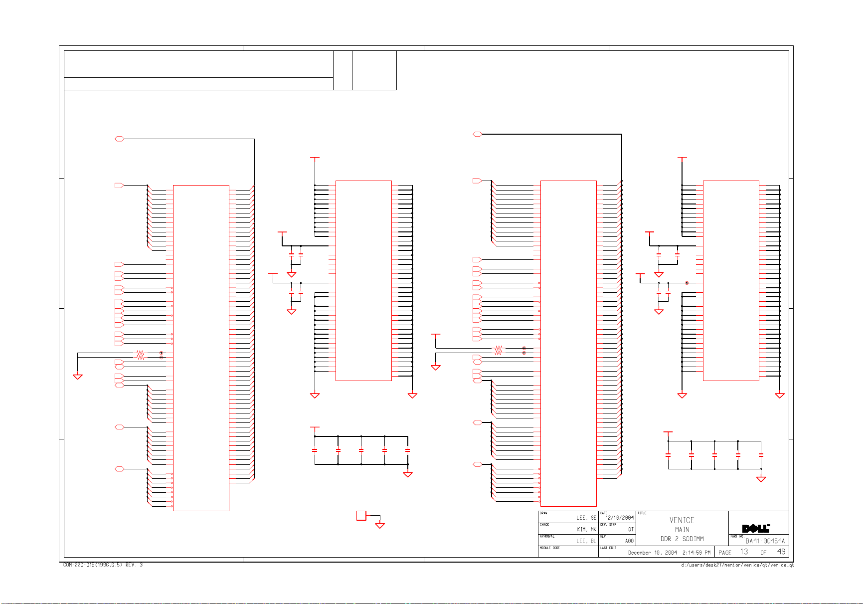
This Sheet of Engineering drawings and specifications contains Confidential,
Trade Secret and other Proprietary information of Dell Computer Corporation ( "Dell" ).
This document may not be transferred or copied without the express written authorization of Dell.
In addition, neither this sheet nor the information it contains may be used by or
disclosed to any third party without Dell’s express written consent.
This drawing is property of SEC, Use or copy of this drawing without proper permission
of the appropriate technical-document managing department is prohibited
4
3
2
1
Rev.
No
D
C
B
A
MEM1_ADQ(63:0)
MEM1_AMA(13:0)
MEM1_ABS2*
MEM1_ABS0*
MEM1_ABS1*
MEM1_CS0*
MEM1_CS1*
CLK1_MCLK0
CLK1_MCLK0*
CLK1_MCLK1
CLK1_MCLK1*
MEM1_CKE0
MEM1_CKE1
MEM1_ACAS*
MEM1_ARAS*
MEM1_AWE*
CLK3_SMBCLK
CLK3_SMBDATA
MEM1_ODT0
MEM1_ODT1
MEM1_ADM(7:0)
MEM1_ADQS(7:0)
MEM1_ADQS*(7:0)
10-B4 14-D4
10-C4 14-C3
10-C4 14-C3
9-B1 14-D3
9-B1 14-D3
9-C1
9-C1
9-C1
9-C1
9-B1
9-B1 14-C3
10-B4 14-C3
10-B4 14-C3
R231
R230
48-C2
4-A4 13-B24-B4
4-A4 13-B24-B4
4-B3
49-C3
9-B1
9-B1 14-C3
13-D210-D4
0
1
2
3
4
5
6
7
8
9
10
11
12
13
14-C310-C4
14-C3
14-C310-B4
10K
10K
4-B3
14-C3
13-B210-C4
0
1
2
3
4
5
6
7
13-B210-C4
0
1
2
3
4
5
6
7
13-A210-C4
0
1
2
3
4
5
6
7
SMBUS ADDR " A0h"
DDR1-1
DDR2-SODIMM-200P-STD
1/2
102
A0
101
A1
100
A2
99
A3
98
A4
97
A5
94
A6
92
A7
93
A8
91
A9
105
A10_AP
90
A11
89
A12
116
A13
86
A14
84
A15
85
A16_BA2
107
BA0
106
BA1
110
S0*
115
S1*
30
CK0
32
CK0*
164
CK1
166
CK1*
79
CKE0
80
CKE1
113
CAS*
108
RAS*
109
WE*
198
SA0
200
SA1
197
SCL
195
SDA
114
ODT0
119
ODT1
10
DM0
26
DM1
52
DM2
67
DM3
130
DM4
147
DM5
170
DM6
185
DM7
13
DQS0
31
DQS1
51
DQS2
70
DQS3
131
DQS4
148
DQS5
169
DQS6
188
DQS7
11
DQS*0
29
DQS*1
49
DQS*2
68
DQS*3
129
DQS*4
146
DQS*5
167
DQS*6
186
DQS*7
DDR2 SO-DIMM #0
Bottom
P1.8V_AUX
DDR1-2
DDR2-SODIMM-200P-STD
112
C885
2200nF
10V
VDD1
111
VDD2
117
VDD3
96
VDD4
95
VDD5
118
VDD6
81
VDD7
82
VDD8
87
VDD9
103
VDD10
88
VDD11
104
VDD12
199
VDDSPD
83
NC1
120
NC2
50
NC3
69
NC4
163
NCTEST
1
VREF
201
GND0
202
GND1
47
VSS1
133
VSS2
183
VSS3
77
VSS4
12
VSS5
48
VSS6
184
VSS7
78
VSS8
71
VSS9
72
VSS10
121
VSS11
122
VSS12
196
VSS13
193
VSS14
8
VSS15
C869
2200nF
10V
CONTACT-PLATE-EMI
EMI4
EMI
0
5
DQ0
1
7
DQ1
2
17
DQ2
3
19
DQ3
4
4
DQ4
5
6
DQ5
6
14
DQ6
7
16
DQ7
8
23
DQ8
25
DQ9
10
35
DQ10
11
37
DQ11
12 13
20
DQ12
13
22
DQ13
14
36
DQ14
15
38
DQ15
16
43
DQ16
17
45
DQ17
18
55
DQ18
19
57
DQ19
20
44
DQ20
21
46
DQ21
22
56
DQ22
23
58
DQ23
24
61
DQ24
25
63
DQ25
26
73
DQ26
27
75
DQ27
28
62
DQ28
29
64
DQ29
30
74
DQ30
31
76
DQ31
32
123
DQ32
33
125
DQ33
34
135
DQ34
35
137
DQ35
36
124
DQ36
37
126
DQ37
38
134
DQ38
39
136
DQ39
40
141
DQ40
41
143
DQ41
42
151
DQ42
43
153
DQ43
44
140
DQ44
45
142
DQ45
46
152
DQ46
47 5
154
DQ47
48
157
DQ48
49
159
DQ49
50
173
DQ50
51
175
DQ51
52
158
DQ52
53
160
DQ53
54
174
DQ54
55
176
DQ55
56
179
DQ56
57
181
DQ57
58
189
DQ58
59
191
DQ59
60
180
DQ60
61
182
DQ61
62
192
DQ62
63
194
DQ63
9
P3.3V
C862
100nF
16V
MEM1_VREF
C890
100nF
16V
C861
2200nF
10V
C294
2200nF
10V
P1.8V_AUX
C282
2200nF
10V
VSS16
VSS17
VSS18
VSS19
VSS20
VSS21
VSS22
VSS23
VSS24
VSS25
VSS26
VSS27
VSS28
VSS29
VSS30
VSS31
VSS32
VSS33
VSS34
VSS35
VSS36
VSS37
VSS38
VSS39
VSS40
VSS41
VSS42
VSS43
VSS44
VSS45
VSS46
VSS47
VSS48
VSS49
VSS50
VSS51
VSS52
VSS53
VSS54
VSS55
VSS56
VSS57
18
24
41
53
42
54
59
65
60
66
127
139
128
145
165
171
172
177
187
178
190
9
21
33
155
34
132
144
156
168
2
3
15
27
39
149
161
28
40
138
150
162
C292
2200nF
10V
C280
2200nF
10V
P3.3V
MEM1_ADQ(63:0)
MEM1_BMA(13:0)
MEM1_BBS2*
MEM1_BBS0*
MEM1_BBS1*
MEM1_CS2*
MEM1_CS3*
CLK1_MCLK3
CLK1_MCLK3*
CLK1_MCLK4
CLK1_MCLK4*
MEM1_CKE2
MEM1_CKE3
MEM1_BCAS*
MEM1_BRAS*
MEM1_BWE*
CLK3_SMBCLK
CLK3_SMBDATA
MEM1_ODT2
MEM1_ODT3
MEM1_ADM(7:0)
MEM1_ADQS(7:0)
MEM1_ADQS*(7:0)
10-C4
13-B4
10-C4
13-B4
10-C4
13-A4
10-B2 14-B4
10-C2 14-C3
10-C2
9-C1
9-B1
9-C1
9-B1
10-B2 14-B3
R825
R824
9-B1 14-C3
9-B1 14-C3
13-D410-D4
0
1
2
3
4
5
6
7
8
9
10
11
12
14-C310-C2
14-C3
14-C39-B1
14-C39-B1
14-C39-B1
14-C39-B1
14-B310-B2
14-B310-B2
10K
10K
4-B3 4-B4 13-B44-A4 48-C2
49-C34-B3 4-B4 13-B44-A4
0
1
2
3
4
6
7
0
1
2
3
4
5
6
7
0
1
2
3
4
5
6
7
SMBUS ADDR " A2h"
DDR2 SO-DIMM #1
Top
DDR500-1
DDR2-SODIMM-200P-RVS
1/2 2/22/2
102
A0
101
A1
100
A2
99
A3
98
A4
97
A5
94
A6
92
A7
93
A8
91
A9
105
A10_AP
90
A11
89
A12
116
A13
86
A14
84
A15
85
A16_BA2
107
BA0
106
BA1
110
S0*
115
S1*
30
CK0
32
CK0*
164
CK1
166
CK1*
79
CKE0
80
CKE1
113
CAS*
108
RAS*
109
WE*
198
SA0
200
SA1
197
SCL
195
SDA
114
ODT0
119
ODT1
10
DM0
26
DM1
52
DM2
67
DM3
130
DM4
147
DM5
170
DM6
185
DM7
13
DQS0
31
DQS1
51
DQS2
70
DQS3
131
DQS4
148
DQS5
169
DQS6
188
DQS7
11
DQS*0
29
DQS*1
49
DQS*2
68
DQS*3
129
DQS*4
146
DQS*5
167
DQS*6
186
DQS*7
DQ0
DQ1
DQ2
DQ3
DQ4
DQ5
DQ6
DQ7
DQ8
DQ9
DQ10
DQ11
DQ12
DQ13
DQ14
DQ15
DQ16
DQ17
DQ18
DQ19
DQ20
DQ21
DQ22
DQ23
DQ24
DQ25
DQ26
DQ27
DQ28
DQ29
DQ30
DQ31
DQ32
DQ33
DQ34
DQ35
DQ36
DQ37
DQ38
DQ39
DQ40
DQ41
DQ42
DQ43
DQ44
DQ45
DQ46
DQ47
DQ48
DQ49
DQ50
DQ51
DQ52
DQ53
DQ54
DQ55
DQ56
DQ57
DQ58
DQ59
DQ60
DQ61
DQ62
DQ63
D
P1.8V_AUX
DDR500-2
DDR2-SODIMM-200P-RVS
0
5
1
7
2
17
3
19
4
4
5
6
6
14
7
16
8
23
9
25
10
35
11
37
12
20
13
22
14
36
15
38
16
43
17
45
18
55
19
57
20
44
21
46
22
56
23
58
24
61
25
63
26
73
27
75
28
62
29
64
30
74
31
76
32
123
33
125
34
135
35
137
36
124
37
126
38
134
39
136
40
141
41
143
42
151
43
153
44
140
45
142
46
152
47
154
48
157
49
159
50
173
51
175
52
158
53
160
54
174
55
176
56
179
57
181
58
189
59
191
60
180
61
182
62
192
63
194
P3.3V
MEM1_VREF
C854
100nF
16V
C271
100nF
P1.8V_AUX
C855
2200nF
10V
C871
2200nF
C272
2200nF
10V
112
111
117
96
95
118
81
82
87
103
88
104
199
83
120
50
69
163
1
201
202
47
133
183
77
12
48
184
78
71
72
121
122
196
193
8
C879
2200nF
10V
VDD1
VDD2
VDD3
VDD4
VDD5
VDD6
VDD7
VDD8
VDD9
VDD10
VDD11
VDD12
VDDSPD
NC1
NC2
NC3
NC4
NCTEST
VREF
GND0
GND1
VSS1
VSS2
VSS3
VSS4
VSS5
VSS6
VSS7
VSS8
VSS9
VSS10
VSS11
VSS12
VSS13
VSS14
VSS15
C881
2200nF
10V
VSS16
VSS17
VSS18
VSS19
VSS20
VSS21
VSS22
VSS23
VSS24
VSS25
VSS26
VSS27
VSS28
VSS29
VSS30
VSS31
VSS32
VSS33
VSS34
VSS35
VSS36
VSS37
VSS38
VSS39
VSS40
VSS41
VSS42
VSS43
VSS44
VSS45
VSS46
VSS47
VSS48
VSS49
VSS50
VSS51
VSS52
VSS53
VSS54
VSS55
VSS56
VSS57
C876
2200nF
10V10V
18
24
41
53
42
54
59
65
60
66
127
139
128
145
165
171
172
177
187
178
190
9
21
33
155
34
132
144
156
168
2
3
15
27
39
149
161
28
40
138
150
162
C873
2200nF
10V
C
B
A
SAMSUNG
4
3
2
1
Page 14
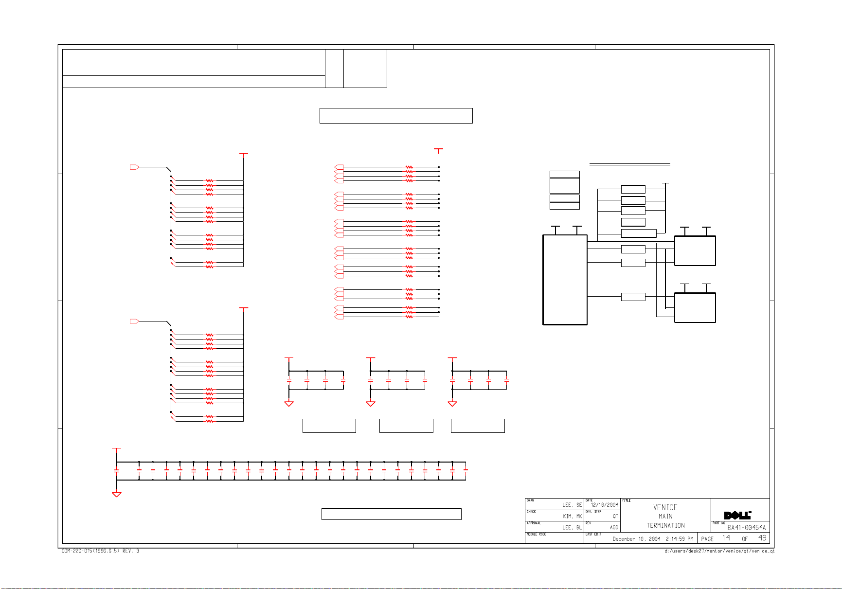
This Sheet of Engineering drawings and specifications contains Confidential,
Trade Secret and other Proprietary information of Dell Computer Corporation ( "Dell" ).
This document may not be transferred or copied without the express written authorization of Dell.
In addition, neither this sheet nor the information it contains may be used by or
disclosed to any third party without Dell’s express written consent.
This drawing is property of SEC, Use or copy of this drawing without proper permission
of the appropriate technical-document managing department is prohibited
4
3
2
1
Rev.
No
D
MEM_0.9V
MEM1_AMA(13:0) MEM1_CS0*
C
MEM1_BMA(13:0)
B
10-B4
13-C4
10-B2
13-C2
0
1
2
3
4
5
6
7
8
9
10
11
12
13
0
1
2
3
4
5
6
7
8
9
10
11
12
13
RA503-2
RA5-2
RA506-1
RA5-1
RA506-2
RA6-2
RA509-1
RA509-2
RA6-1
RA7-2
RA4-1
RA511-1
RA7-1
RA500-2
RA515-2
RA507-2
RA516-1
RA507-1
RA516-2
RA508-2
RA517-1
RA517-2
RA508-1
RA510-2
RA505-1
RA518-1
RA510-1
RA513-1
34
34
12
12
34
34
12
34
12
34
2
1
12
12
34
34
34
12
12
34
34
12
34
12
34
12
12
12
12
56
56
56
56
56
56
56
56
56
56
56
56
56
56
56
56
56
56
56
56
56
56
56
56
56
56
56
56
MEM_0.9V
P1.8V_AUX
100nF 100nF
Array resistors & Single resistors used to improve layout & routing.
MEM_0.9V
12
MEM1_CS1*
MEM1_CS2*
MEM1_CS3*
MEM1_CKE0
MEM1_CKE1
MEM1_CKE2
MEM1_CKE3
MEM1_ODT0
MEM1_ODT1
MEM1_ODT2
MEM1_ODT3
MEM1_ABS0*
MEM1_ABS1*
MEM1_ABS2*
MEM1_ACAS*
MEM1_ARAS*
MEM1_AWE*
MEM1_BBS0*
MEM1_BBS1*
MEM1_BBS2*
MEM1_BCAS*
MEM1_BRAS*
MEM1_BWE*
13-C49-B1
13-C49-B1
13-C29-B1
13-C29-B1
13-B49-B1
13-B49-B1
13-B29-B1
9-B1 13-B2
13-B4
9-B1
9-B1 13-B4
9-B1 13-B2
13-B29-B1
10-C4 13-C4
13-C4
10-C4
13-C410-C4
13-B410-B4
10-B4 13-B4
10-B4 13-B4
13-C210-C2
13-C210-C2
10-C2 13-C2
10-B2 13-B2
13-B210-B2
13-B210-B2
RA501-1
RA2-1
RA514-1
RA502-1
RA8-1
RA511-2
RA512-1
RA518-2
RA500-1
RA2-2
RA513-2
RA502-2
RA4-2
RA503-1
RA8-2
RA3-2
RA501-2
RA3-1
RA505-2
RA515-1
RA512-2
RA504-2
RA514-2
RA504-1
12
12
12
12
34
12
34
12
34
34
34
4
3
12
34
34
34
12
4
3
2
1
4
3
34
34
12
56
56
56
56
56
56
56
56
56
56
56
56
56
56
56
56
56
56
56
56
56
56
56
56
P1.8V_AUX P1.8V_AUX
C874
C884C273
100nF
100nF 100nF
C287
C883C878
Place near GMCH
C847C850
100nF100nF
Place near SO-DIMM0
100nF100nF
C844
100nF
Place near SO-DIMM1
C835 C840
100nF
100nF
C842
VCCSM
DDR-II ::
P1.8V_AUX
VCCA_SM
P1.5V
VCCA_SM
VCCSM
Channel A
Alviso-GM
Memory Topology
( Single channel for DDR-II )
(TBD) "
(TBD) "
(TBD) "
(TBD) "
(TBD) "
(TBD) "
(TBD) "
(TBD) "
Address
CS
CKE
BS
CAS/RAS/WE
DQ(63:0)
CLK
CLK
P0.9V
P3.3V
P1.8V_AUX
DDR-II
Standard
Connector
Memory Channel A-1
P1.8V_AUX
P3.3V
DDR-II
Reverse
Connector
Memory Channel A-2
Bottom
Top
D
C
B
MEM_0.9V
C288
C872
C839
A
C843
100nF
16V
C852
100nF
16V
100nF
16V
C841
100nF 100nF
16V
C283
16V
C837
100nF
16V
C880
100nF
16V
C849
100nF
16V
C882
100nF
16V
C875
100nF
16V
C286
100nF
16V
C845
100nF
16V
C853
16V
C877
C836
100nF
100nF
16V16V
C846
100nF
16V
100nF
100nF100nF
16V16V
C848
100nF
16V
C870
100nF
16V
C285
100nF
16V
C281
100nF
16V
Place one cap close to every 2 pull-up resistors terminated to P0.9V
4
3
C291
100nF
16V 16V
C838
100nF
C851
100nF
16V
C290
100nF
16V
A
SAMSUNG
2
1
Page 15
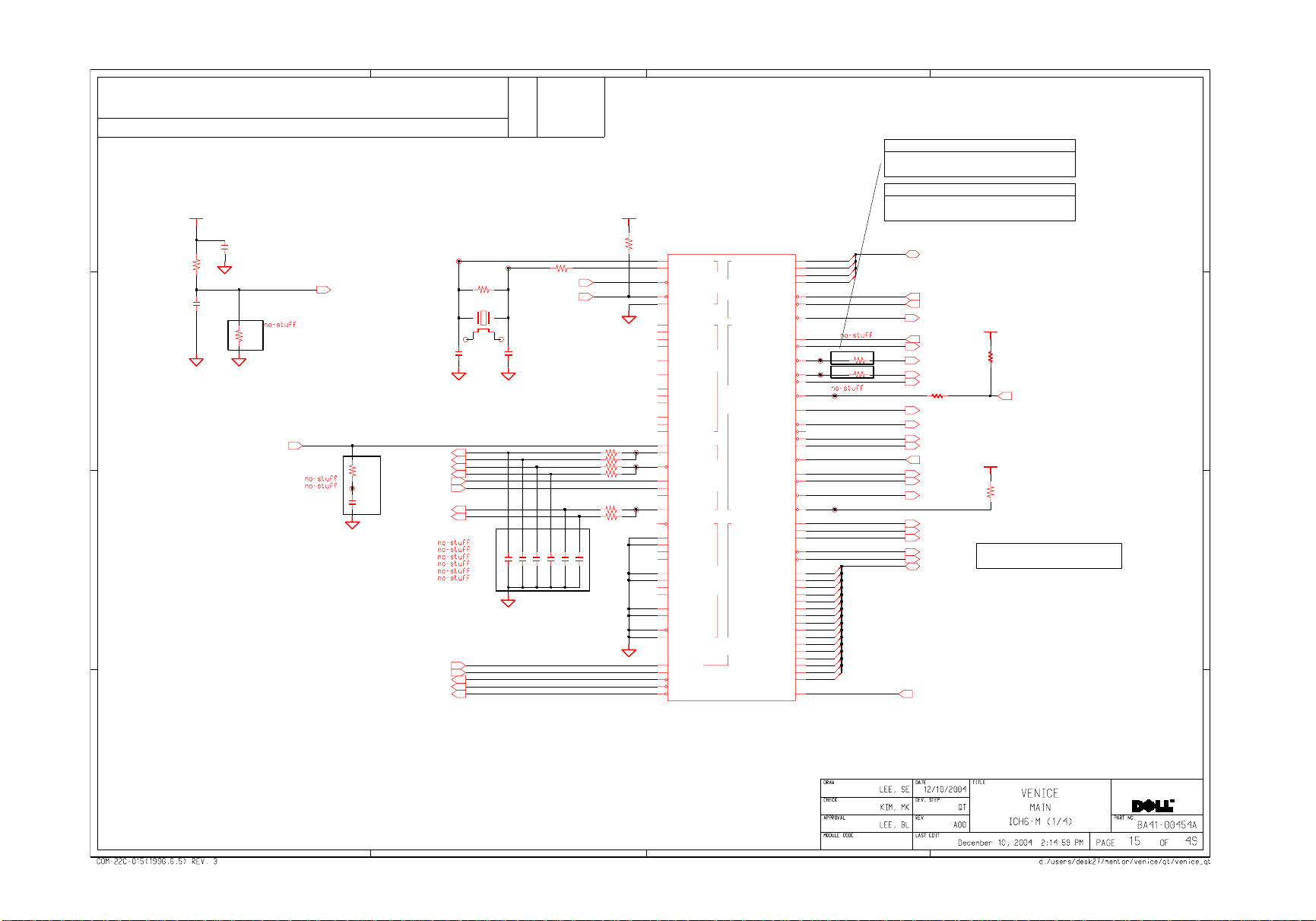
This Sheet of Engineering drawings and specifications contains Confidential,
Trade Secret and other Proprietary information of Dell Computer Corporation ( "Dell" ).
This document may not be transferred or copied without the express written authorization of Dell.
In addition, neither this sheet nor the information it contains may be used by or
disclosed to any third party without Dell’s express written consent.
This drawing is property of SEC, Use or copy of this drawing without proper permission
of the appropriate technical-document managing department is prohibited
D
VCC_RTC
C113
1000nF
R86
20K
1%
C114
1000nF
6.3V
R167
100K
CHP3_RTCRST*
15-C349-A4
For RTC reset
R640
32.768KHz
14
23
C603
0.01nF
Y500
C
AUD3_AC97_BCLK
26-C4 49-D2
R181
47
C208
0.027nF
AUD3_AC97_SYNC
MDC3_AC97_SYNC
AUD3_AC97_RST*
MDC3_AC97_RST*
AUD3_AC97_SDI0
MDC3_AC97_SDI1
AUD3_AC97_SDO
MDC3_AC97_SDO
49-D226-C4
33-C2
26-C4 49-D2
33-C2
26-C4 49-D2
33-C2
49-B326-C4
33-C2 49-A3
B
IDE3_IORDY
IDE3_IDEIRQ
IDE3_DACK*
IDE3_IOW*
IDE3_IOR*
48-B332-C1
18-C3 49-D432-C1
48-B332-C1
48-C332-C1
48-C3
32-C1
34
Rev.
No
10M
CHP3_INTRUDER*
C651
0.01nF
0.01nF
0.5pF
0.01nF
C163
C162
R641
CHP3_RTCRST*
0.01nF
0.01nF
0.5pF
0.5pF
C207
C206
0.5pF
0.01nF
C166
0
0.5pF
R156
R155
R180
R182
R158
R157
0.01nF
C165
0.5pF
VCC_RTC
49-A415-C4
49-D231-C2
33 1%
33 1%
33 1%
33
33 1%
33 1%
U515-1
82801FBM(DELL)
R84
680K
1 / 5
1%
Y1
RTCX1
Y2
RTCX2
AA2
RTCRST*
AA3
INTRUDER*
AA5
INTVRMEN
D12
EE_CS
B12
EE_SHCLK
D11
EE_DOUT
F13
EE_DIN
F12
LAN_CLK
B11
LAN_RSTSYNC
E12
LANRXD0
E11
LANRXD1
C13
LANRXD2
C12
LANTXD0
C11
LANTXD1
E13
LANTXD2
C10
ACZ_BIT_CLK
B9
ACZ_SYNC
A10
ACZ_RST*
1%
F11
ACZ_SDIN0
F10
ACZ_SDIN1
B10
ACZ_SDIN2
C9
ACZ_SDO
AC19
SATALED*
AE3
SATA0RXN
AD3
SATA0RXP
AG2
SATA0TXN
AF2
SATA0TXP
AD7
SATA2RXN
AC7
SATA2RXP
AF6
SATA2TXN
AG6
SATA2TXP
AC2
SATA_CLKN
AC1
SATA_CLKP
AG11
SATARBIAS*
AF11
SATARBIAS
AF16
IORDY
AB16
IDEIRQ
AB15
DDACK*
AC14
DIOW*
AE16
DIOR*
LAD0_FWH0
LAD1_FWH1
LAD2_FWH2
LAD3_FWH3
RTC
LPCCPUIDE
LDRQ1*_GPI41
LFRAME*_FWH4
LANAZALIA
DPRSLP*_TP4
DPSLP*_TP2
CPUPWRGD_GPO49
THRMTRIP*
SATA
LDRQ0*
A20GATE
A20M*
CPUSLP*
FERR*
IGNNE*
INIT3_3V*
INIT*
INTR
RCIN*
NMI
SMI*
STPCLK*
DA0
DA1
DA2
DCS1*
DCS3*
DD0
DD1
DD2
DD3
DD4
DD5
DD6
DD7
DD8
DD9
DD10
DD11
DD12
DD13
DD14
DD15
DDREQ
2
1
CPUSLP*
Dothan A stepping : Stuff resistor on SLP* of ICH6-M
Dothan B stepping ~ : Stuff resistor on SLP of GMCH.
D
DPRSTP*
Dothan : No stuff
Yonah : Stuff
P2
N3
N5
N4
N6
P4
P3
AF22
AF23
AE27
AE24
AD27
AF24
AG25
AG26
AE22
AF27
AG24
AD23
AF25
AG27
AE26
AE23
AC16
AB17
AC17
AD16
AE17
AD14
AF15
AF14
AD12
AE14
AC11
AD11
AB11
AE13
AF13
AB12
AB13
AC13
AE15
AG15
AD13
AB14
10
11
12
13
14
15
R195
R193
0
1
2
3
4
5
6
7
8
9
27-C2
0
1
2
3
48-C2 28-A2
48-C2 27-C2
27-C249-B3 24-B4
48-C3 28-B2
0
0
49-D3 6-C3
48-B4
48-C4 32-C1
48-C4 32-C1
48-C4 32-C2
48-D3 32-C1
48-D3 32-C2
48-C3
48-D3
48-C3 32-C1
LPC3_LAD(3:0)
24-C4
49-B4
CHP3_LDRQ0*
CHP3_LDRQ1*
LPC3_LFRAME*
KBC3_A20G
CPU1_A20M*
5-C348-C3
CPU1_SLP*
6-C3
8-A2
48-C4
CPU1_DPRSTP*
6-C349-C3
CPU1_DPSLP*
12
RA1-1
CPU1_PWRGDCPU
6-C4
CPU1_IGNNE*
5-B349-D3
CPU1_INIT*
5-C348-B3
CPU1_INTR
5-B348-C4
KBC3_ICH6RCIN*
27-B349-C2
CPU1_NMI
5-B3
CPU1_SMI*
5-B348-C4
CPU1_STPCLK*
5-B349-C3
IDE3_A0
IDE3_A1
IDE3_A2
IDE3_CS1*
IDE3_CS3*
IDE3_D(15:0)
32-D2
48-B3
IDE3_DREQ
VTT
3
RA1-2
56
4
56
CPU1_FERR*
5-B348-B3
VTT
R194
47
Place 56 ohm resistor within 2" of ICH6-M
Place PU resistor within 2" of ICH6-M
C
B
A
A
SAMSUNG
4
3
2
1
Page 16

0
1
2
3
4
5
6
7
8
9
10
11
12
13
14
15
16
17
18
19
20
21
22
23
24
25
26
27
28
29
30
31
34-B222-B3
35-B2
35-B2 48-C2
34-C2 48-C218-C3
23-C4 48-C218-C3
23-D4 34-C3
4
U515-2
82801FBM(DELL)
2 / 5
E2
AD0
E5
AD1
C2
AD2
F5
AD3
F3
AD4
E9
AD5
F2
AD6
D6
AD7
E6
AD8
D3
AD9
A2
AD10
D2
AD11
D5
AD12
H3
AD13
B4
AD14
J5
AD15
K2
AD16
K5
AD17
D4
AD18
L6
AD19
G3
AD20
H4
AD21
H2
AD22
H5
AD23
B3
AD24
M6
AD25
B2
AD26
K6
AD27
K3
AD28
A5
AD29
L1
AD30
K4
AD31
J3
FRAME*
N2
PIRQA*
L2
PIRQB*
M1
PIRQC*
L3
PIRQD*
AC5
RSVD1_SATA1RXN
AD5
RSVD2_SATA1RXP
AF4
RSVD3_SATA1TXN
AG4
RSVD4_SATA1TXP
AC9
RSVD5_SATA3RXN
PCI
INTERRUPT I/F
RESERVED
REQ0*
GNT0*
REQ1*
GNT1*
REQ2*
GNT2*
REQ3*
GNT3*
REQ4*_GPI40
GNT4*_GPO48
REQ5*_GPI1
GNT5*_GPO17
REQ6*_GPI0
GNT6*_GPO16
C_BE0*
C_BE1*
C_BE2*
C_BE3*
IRDY*
PAR
PCIRST*
DEVSEL*
PERR*
PLOCK*
SERR*
STOP*
TRDY*
PLTRST*
PCICLK
PME*
PIRQE*_GPI2
PIRQF*_GPI3
PIRQG*_GPI4
PIRQH*_GPI5
RSVD6_SATA3RXP
RSVD7_SATA3TXN
RSVD8_SATA3TXP
RSVD9_TP3
L5
C1
B5
B6
M5
F1
B8
C8
F7
E7
E8
F6
B7
D8
J6
H6
G4
G2
A3
E1
R2
C3
E3
C5
G5
J1
J2
R5
G6
P6
D9
C7
C6
M3
AD9
AF8
AG8
U3
R147
R146
R148
R149
P3.3V
1%100
10K
0
10K
48-C2 35-B2 34-B2 22-B3
48-C2 35-B2 34-C3
48-C2
R150
R151
R153
R94
R143
33
1%
C158
0.027nF
18-C348-C2 36-C1
35-B235-C248-C2
18-B3
18-C348-C2 22-B3
22-B348-C2 18-B3
18-C3
18-B348-C2 34-C3
34-C248-C2 18-B3
18-B3
19-D2
49-A3
22-B348-C2 35-B2 34-B3
34-B3 22-B348-C2 35-B2
22-B3
22-B334-B335-B2 18-C335-C248-C2
22-B334-B235-B2 18-C348-B4
34-C235-B248-C3 22-B3
22-B334-B235-B2 18-C349-B3
22-B3
34-B335-B2 18-C348-C2
35-B249-A4 18-C3
22-B334-B335-B2 18-C348-C2
22-B334-B235-B2 18-C348-C2
22-B334-B235-B2 18-C3
16-B448-C2
27-B348-C4 18-B3
10K
10K
10K
10K
This Sheet of Engineering drawings and specifications contains Confidential,
Trade Secret and other Proprietary information of Dell Computer Corporation ( "Dell" ).
This document may not be transferred or copied without the express written authorization of Dell.
In addition, neither this sheet nor the information it contains may be used by or
disclosed to any third party without Dell’s express written consent.
This drawing is property of SEC, Use or copy of this drawing without proper permission
of the appropriate technical-document managing department is prohibited
D
PCI3_AD(31:0)
35-C4 #4
22-D3
22-B3
34-C2 34-D4
35-B4
35-B2
C
PCI3_FRAME*
PCI3_INTA*
PCI3_INTB*
PCI3_INTC*
PCI3_INTD*
18-C3
49-B4 35-C2
18-C3
18-C3
48-C2
B
P3.3V_AUX
U14
5
7SZ08
1
PLT3_RSTF*
A
ICH_PWROK
16-C3 48-C2
16-B2 30-B2
31-D4 48-D3
+
4
2
-
3
R85
PLT3_RST* ICH_PWROK
24-B4
16-A2
21-B3
27-D2
24-C4 9-A2
48-C3
100K
CLK3_ICH14
CLK3_USB48
4-B1 16-B2 48-C3
4-C3
48-C316-B2
R207
10
C244
0.01nF
0.5pF
PGND
Place near the ICH6-M
3
4-C349-C2
P3.3V
Rev.
No
PCI3_REQ0*
PCI3_GNT0*
PCI3_REQ1*
PCI3_GNT1*
PCI3_REQ2*
PCI3_REQ3*
PCI3_GNT3*
CHP3_REQ5*
LCD5_LAMPSTAT
PCI3_CBE0*
PCI3_CBE1*
PCI3_CBE2*
PCI3_CBE3*
PCI3_IRDY*
PCI3_PAR
PCI3_RST*
PCI3_DEVSEL*
PCI3_PERR*
PCI3_PLOCK*
PCI3_SERR*
PCI3_STOP*
PCI3_TRDY*
PLT3_RSTF*
CLK3_PCLKICH6M
CHP3_PME*
R144
10
C159
0.0033nF
SMB3_CLK
SMB3_DATA
SMB3_LINKALERT*
CHP3_SPKR
MCH2_BMBUSY*
KBC3_EXTSMI*
SMB3_ALERT*
KBC3_WAKESCI*
KBC3_RUNSCI*
CHP3_PCISTP*
CHP3_CPUSTP*
TPM_RST*
PCI3_CLKRUN*
KBC3_PCIE_WAKE*
CHP3_SERIRQ
KBC3_THRM*
IMVP_PWRGD
CLK3_ICH14
CLK3_USB48
CHP3_SLPS3*
CHP3_SLPS5*
CHP3_DPRSLPVR
KBC3_PWRBTN*
PLT3_RST*
SUSPWROK
4-C4 18-B3 24-B4 48-B4
18-B3
26-C1 48-C4
P3.3V
9-A3
49-B3
49-C327-C3
18-B3
49-A327-B3
27-B3 49-C3
49-A44-C3
6-C4 41-C4 49-A44-C3
24-C4
P3.3V_AUX
27-C2 34-B3
18-C3 49-B323-C4
18-B3 49-B227-B3
23-C4 24-B4 27-C218-C3 48-C2
27-B3 48-B328-C1
9-A2 31-A430-B327-C3
4-B1 48-C316-A3
4-C3 48-C316-A3
P3.3V_AUX
27-B3 48-C2
27-B3 48-C2
16-A4
30-B2 31-D4 48-D3
41-C4 49-B3
27-B3 49-C3
30-C2 48-B431-D3
18-B324-B4 48-B34-C4
P3.3V_AUX
R172
R175
R177
10K
R171
R168
100K
P3.3V
48-B3
R173
R87
R90
10K
R169
10K
10K
0
R138
0
R89
10K
R136
48-C327-D224-C416-B4 21-B3 24-B49-A2
2
P3.3V_AUX
U515-3
82801FBM(DELL)
R91
10K
10K
3 / 5
T2
RI*
AF17
R88
SATA0GP_GPI26
AE18
SATA1GP_GPI29
AF18
SATA2GP_GPI30
AG18
SATA3GP_GPI31
Y4
SMBCLK
W5
SMBDATA
Y5
LINKALERT*
W4
SMLINK0
U6
SMLINK1
AG21
MCH_SYNC*
F8
SPKR
W3
SUS_STAT*_LPCPD*
10K
U2
SYS_RESET*
AD19
BMBUSY*_GPI6
AE19
GPI7
R1
GPI8
W6
SMBALERT*_GPI11
M2
GPI12
R6
GPI13
AC21
STP_PCI*_GPO18
AB21
GPO19
AD22
STP_CPU*_GPO20
AD20
GPO21
AD21
GPO23
V3
GPIO24
P5
GPIO25
R3
GPIO27
T3
GPIO28
AF19
CLKRUN*_GPIO32
AF20
GPIO33
AC18
GPIO34
U5
WAKE*
AB20
SERIRQ
AC20
THRM*
AF21
VRMPWRGD
E10
CLK14
A27
CLK48
V6
SUSCLK
T4
SLP_S3*
T5
SLP_S4*
T6
SLP_S5*
AA1
PWROK
100
AE20
DPRSLPVR_TP1
1%
10K
V2
BATLOW*_TP0
U1
PWRBTN*
V5
LAN_RST*
100
Y3
RSMRST*
1%
R131
100K
PCI-EXPRESS
GPIO
DIRECT MEDIA INTERFACEUSB
DMI_CLKN
DMI_CLKP
DMI_ZCOMP
DMI_IRCOMP
OC4*_GPI9
OC5*_GPI10
OC6*_GPI14
OC7*_GPI15
CLOCKSPOWER MGT
USBRBIAS*
USBRBIAS
PERN1
PERP1
PETN1
PETP1
PERN2
PERP2
PETN2
PETP2
PERN3
PERP3
PETN3
PETP3
PERN4
PERP4
PETN4
PETP4
DMI0RXN
DMI0RXP
DMI0TXN
DMI0TXP
DMI1RXN
DMI1RXP
DMI1TXN
DMI1TXP
DMI2RXN
DMI2RXP
DMI2TXN
DMI2TXP
DMI3RXN
DMI3RXP
DMI3TXN
DMI3TXP
OC0*
OC1*
OC2*
OC3*
USBP0N
USBP0P
USBP1N
USBP1P
USBP2N
USBP2P
USBP3N
USBP3P
USBP4N
USBP4P
USBP5N
USBP5P
USBP6N
USBP6P
USBP7N
USBP7P
1
AC caps : PCIE need to be within 250mils of the driver
Resistor for Test : Place Stuffing Option to minimize stubs
H25
H24
G27
G26
K25
K24
J27
J26
M25
M24
L27
L26
P24
P23
N27
N26
T25
T24
R27
R26
V25
V24
U27
U26
Y25
Y24
W27
W26
AB24
AB23
AA27
AA26
AD25
AC25
F24
F23
C23
D23
C25
C24
C27
B27
B26
C26
C21
D21
A20
B20
D19
C19
A18
B18
E17
D17
B16
A16
C15
D15
A14
B14
A22
B22
R179
22.6
100nFC239
100nFC238
9-C1
9-C1
9-D1
9-C1
9-C1
9-C1
9-C1
9-C1
4-C1
4-C1
Place within 500 mils of ICH6-M
1%
10V
10V
24-C4
24-C4
24-C4
24-C4
DMI1_RXN0
DMI1_RXP0
DMI1_TXN0
DMI1_TXP0
DMI1_RXN1
DMI1_RXP1
DMI1_TXN1
DMI1_TXP1
CLK1_PCIEICH*
CLK1_PCIEICH
32-C4
32-C4
36-B2
36-B2
33-B3
33-B3
32-A4
32-A4
32-A4
32-A4
23-C3
23-C3
PEX1_RXN1
PEX1_RXP1
PEX1_TXN1
PEX1_TXP1
USB3_P0USB3_P0+
USB3_P1USB3_P1+
USB3_P2USB3_P2+
USB3_P3USB3_P3+
USB3_P4USB3_P4+
USB3_P5USB3_P5+
Place 24.9ohm wthin 500 mils of ICH6-M
P3.3V_AUX
P1.5V
10K
10K
10K
10K
10K
10K
10K
10K
R202
R199
R206
R198
R201
R200
R203
R204
24.9
R197
1%
USB3_OC4*
32-B448-B3
USB3_OC0*
48-B3 32-D4
USB3_OC3*
48-B3 32-B4
SAMSUNG
D
C
B
A
4
3
2
1
Page 17

This Sheet of Engineering drawings and specifications contains Confidential,
Trade Secret and other Proprietary information of Dell Computer Corporation ( "Dell" ).
This document may not be transferred or copied without the express written authorization of Dell.
In addition, neither this sheet nor the information it contains may be used by or
disclosed to any third party without Dell’s express written consent.
This drawing is property of SEC, Use or copy of this drawing without proper permission
of the appropriate technical-document managing department is prohibited
D
4 2
AA22
AA23
AA24
AA25
AB25
AB26
AB27
P1.5V
B23
BLM18PG181SN1
Place caps within 100mils of ICH6-M
near F27, P27, AB27
C197
C235
100nF
C237
100nF
PGND
150uF
6V
AL
C240
100nF
C
P3.3V
C234
10nF
16V
C144
100nF
P1.5V
C109
C145
100nF
100nF
Place 10nF within 100 mils
of ICH6-M
P1.5V
C194
100nF
C160
100nF
P3.3V
C143
100nF
P3.3V_AUX
C149
C203
100nF
100nF
C157
100nF
AC27
AG10
Place 100nF within 100 mils
near pin AG9
Place 100nF within 100 mils
near pin AG5
P1.5V
B
Place 100nF within 100mils pin E26,E27
Place 100nF within 100mils pin AE1
Place 100nF within 100 mils
near pin AG10
Place 100nF within 100 mils
near pin A13
A
Place 100nF within 100 mils
of ICH6-M pin V7
Place both within 100 mils
near pin A17
R196
C236
10000nF
6.3V
B26
MMZ1608S121AT
1
3
Rev.
No
4 / 5
VCC1_5_1
VCC1_5_2
VCC1_5_3
VCC1_5_4
VCC1_5_5
VCC1_5_6
VCC1_5_7
F25
VCC1_5_8
F26
VCC1_5_9
F27
VCC1_5_10
G22
VCC1_5_11
G23
VCC1_5_12
G24
VCC1_5_13
G25
VCC1_5_14
H21
VCC1_5_15
H22
VCC1_5_16
J21
VCC1_5_17
J22
VCC1_5_18
K21
VCC1_5_19
K22
VCC1_5_20
L21
VCC1_5_21
L22
VCC1_5_22
M21
VCC1_5_23
M22
VCC1_5_24
N21
VCC1_5_25
N22
VCC1_5_26
N23
VCC1_5_27
N24
VCC1_5_28
N25
VCC1_5_29
P21
VCC1_5_30
P25
VCC1_5_31
P26
VCC1_5_32
P27
VCC1_5_33
R21
VCC1_5_34
R22
VCC1_5_35
T21
VCC1_5_36
T22
VCC1_5_37
U21
VCC1_5_38
U22
VCC1_5_39
V21
VCC1_5_40
V22
VCC1_5_41
W21
VCC1_5_42
W22
VCC1_5_43
Y21
VCC1_5_44
Y22
VCC1_5_45
AA6
VCC1_5_46
AB4
VCC1_5_47
AB5
VCC1_5_48
AB6
VCC1_5_49
AC4
VCC1_5_50
AD4
VCC1_5_51
AE4
VCC1_5_52
AE5
VCC1_5_53
AF5
VCC1_5_54
AG5
VCC1_5_55
AA7
VCC1_5_56
AA8
VCC1_5_57
AA9
VCC1_5_58
AB8
VCC1_5_59
AC8
VCC1_5_60
AD8
VCC1_5_61
AE8
VCC1_5_62
AE9
VCC1_5_63
AF9
VCC1_5_64
AG9
VCC1_5_65
VCCDMIPLL
E26
VCC3_3_1
AE1
VCCSATAPLL
VCC3_3_22
A13
VCCLAN3_3_VCCSUS3_3_1
F14
VCCLAN3_3_VCCSUS3_3_2
G13
VCCLAN3_3_VCCSUS3_3_3
G14
VCCLAN3_3_VCCSUS3_3_4
A11
VCCSUS3_3_1
U4
VCCSUS3_3_2
V1
VCCSUS3_3_3
V7
VCCSUS3_3_4
W2
VCCSUS3_3_5
Y7
VCCSUS3_3_6
A17
VCCSUS3_3_7
B17
VCCSUS3_3_8
C17
VCCSUS3_3_9
F18
VCCSUS3_3_10
G17
VCCSUS3_3_11
G18
VCCSUS3_3_12
U515-4
82801FBM(DELL)
VCC1_5_98
VCC1_5_97
VCC1_5_96
VCC1_5_95
VCC1_5_94
VCC1_5_93
VCC1_5_92
VCC1_5_91
VCC1_5_90
VCC1_5_89
COREIDEPCIUSB COREPCI/IDE REF USB
VCC1_5_88
VCC1_5_87
VCC1_5_86
VCC1_5_85
VCC1_5_84
VCC1_5_83
VCC1_5_82
VCC1_5_81
PCIESATA
VCCLAN1_5_VCCSUS1_5_2
VCCLAN1_5_VCCSUS1_5_1
VCC1_5_80
VCC1_5_79
VCC3_3_21
VCC3_3_20
VCC3_3_19
VCC3_3_18
VCC3_3_17
VCC3_3_16
VCC3_3_15
VCC3_3_14
VCC3_3_13
VCC3_3_12
VCC3_3_11
VCC3_3_10
VCC3_3_9
VCC3_3_8
VCC3_3_7
VCC3_3_6
VCC3_3_5
VCC3_3_4
VCC3_3_3
VCC3_3_2
VCCSUS1_5_3
VCCSUS1_5_2
VCCSUS1_5_1
VCC1_5_78
VCC1_5_77
VCC1_5_76
VCC1_5_75
VCC1_5_74
VCC1_5_73
VCC1_5_72
VCC1_5_71
VCC1_5_70
VCC1_5_69
VCC1_5_68
VCC1_5_67
VCC2_5_4
VCC2_5_2
V5REF_2
V5REF_1
V5REF_SUS
VCCUSBPLL
VCCSUS3_3_20
V_CPU_IO_3
V_CPU_IO_2
V_CPU_IO_1
VCCSUS3_3_19
VCCSUS3_3_18
VCCSUS3_3_17
VCCSUS3_3_16
VCCSUS3_3_15
VCCSUS3_3_14
VCCSUS3_3_13
VCCRTC
F9
U17
U16
U14
U12
U11
T17
T11
P17
P11
M17
M11
L17
L16
L14
L12
L11
AA21
AA20
AA19
AA10
AG19
AG16
AG13
AD17
AC15
AA17
AA15
AA14
AA12
P1
M7
L7
L4
J7
H7
H1
E4
B1
A6
U7
R7
G19
G20
F20
E24
E23
E22
E21
E20
D27
D26
D25
D24
G8
AB18
P7
AA18
A8
F21
A25
A24
AB3
G11
G10
AG23
AD26
AB22
G16
G15
F16
F15
E16
D16
C16
P1.5V
P3.3V
C153
100nF
C155
100nF
P1.5V
C198
C241
100nF
100nF
Place near pin AB18
P1.5V
VTT
C233
100nF
Place both within 100 mils
near pin AG23
Place near pin AA19 of the ICH6-M
C110
C151
100nF
C148
100nF
C156
100nF
C196
100nF
100nF
Place 100nF within 100 mils
near pin AG13, AG16
C147
100nF
P1.5V_AUX
Place both within 100 mils
near pin D27
P2.5V
C195
100nF
C154
100nF
Place near pin AB3
Place both within 100 mils
near pin G10
C146
C199
10nF
100nF
16V
Distribute in PCI section near pin A2-A6, near D1-H1
Place near pin U7,R7
C150
C152
C259
100nF
100nF
100nF
Place near pin G19
Place 100nF near pin A8
P5V_AUX
VCC_RTC
R161
10
C161
1000nF
6.3V
C164
100nF
C112
100nF
Place within 100 mils
of ICH6-M (Pin A24)
C111
100nF
P5V_ALW
P3.3V_AUX
C242
100nF
R178
10
C202
1000nF
6.3V
C201
100nF
P1.5V
PGND
C243
10nF
16V
1
Place 100nF near pin F21
Place 10nF within 100 mils
of ICH6-M
SAMSUNG
D
C
B
A
4
3
2
1
Page 18

This Sheet of Engineering drawings and specifications contains Confidential,
Trade Secret and other Proprietary information of Dell Computer Corporation ( "Dell" ).
This document may not be transferred or copied without the express written authorization of Dell.
In addition, neither this sheet nor the information it contains may be used by or
disclosed to any third party without Dell’s express written consent.
This drawing is property of SEC, Use or copy of this drawing without proper permission
of the appropriate technical-document managing department is prohibited
4
D
P3.3V
10K
R101
10K
R170
10K
R102
10K
R99
10K
R103
10K
R105
10K
R98
10K
R100
10K
R106
10K
P3.3V_AUX
R174
R176
R141
R160
R142
R154
R145
R104
R159
R152
R137
R139
R135
R133
R132
R134
R97
R92
R95
R93
R96
10K
10K
10K
10K
10K
10K
10K
10K
10K
10K
10K
10K
10K
10K
1K
10K
2.21k
2.21k
10K
10K
1%
1%
1%
48-C2 16-B227-C2 24-B4
C
B
22-B334-B235-B2 16-C348-B4
23-C427-C234-B3 16-B249-B3
22-B334-B335-B2 16-C348-C2
35-B249-A4
22-B334-B235-B2 16-C349-B3
22-B334-B235-B2 16-C435-C249-B4
22-B334-B235-B2 16-C348-C2
22-B334-B335-B2 16-C348-C2
22-B334-B335-B2 16-C335-C248-C2
22-B334-B235-B2 16-C348-C2
35-B248-C2 16-B4
34-C248-C2 16-B4
23-C448-C2 16-B4
23-D434-C348-C2 16-B4
23-C4
36-C148-C2 16-D3
22-B348-C2 16-D3
34-C348-C2 16-D3
35-B235-C248-C2 16-D3
22-B348-C2 16-D3
48-C2 16-D3
34-C2
49-B2 27-B3 16-B2
48-B3
24-B4 16-D2 4-C4
16-C3
15-A332-C149-D4
16-D3
16-C3
16-C348-C4 27-B3
16-D2
16-C2
4-C416-D224-B448-B4
3
Rev.
No
PCI3_PAR
PCI3_CLKRUN*
PCI3_PERR*
PCI3_PLOCK*
PCI3_DEVSEL*
PCI3_FRAME*
PCI3_STOP*
PCI3_SERR*
PCI3_IRDY*
PCI3_TRDY*
PCI3_INTA*
PCI3_INTB*
PCI3_INTC*
PCI3_INTD*
CHP3_SERIRQ
IDE3_IDEIRQ
PCI3_REQ0*
PCI3_REQ1*
PCI3_REQ2*
PCI3_REQ3*
CHP3_REQ5*
PCI3_GNT0*
PCI3_GNT1*
PCI3_GNT3*
KBC3_PCIE_WAKE*
CHP3_PME*
SMB3_DATA
SMB3_CLK
SMB3_LINKALERT*
SMB3_ALERT*
2
1
U515-5
82801FBM(DELL)
AG22
AG20
AG17
AG14
AG12
AG7
AG3
AG1
AF26
AF12
AF10
AE25
AE21
AE12
AE11
AE10
AD24
AD18
AD15
AD10
AD6
AD2
AD1
AC26
AC24
AC23
AC22
AC12
AC10
AC6
AC3
AB19
AB10
AA16
AA13
AA11
W25
W24
W23
AF7
AF3
AF1
AE7
AE6
AE2
AB9
AB7
AB2
AB1
AA4
Y27
Y26
Y23
V27
V26
V23
U25
U24
U23
U15
U13
T27
T26
T23
T16
T15
T14
T13
T12
R25
R24
R23
R17
R16
R15
R14
R13
R12
R11
W7
W1
Y6
V4
T7
T1
R4
5 / 5
VSS_172
VSS_171
VSS_170
VSS_169
VSS_168
VSS_167
VSS_166
VSS_165
VSS_164
VSS_163
VSS_162
VSS_161
VSS_160
VSS_159
VSS_158
VSS_157
VSS_156
VSS_155
VSS_154
VSS_153
VSS_152
VSS_151
VSS_150
VSS_149
VSS_148
VSS_147
VSS_146
VSS_145
VSS_144
VSS_143
VSS_142
VSS_141
VSS_140
VSS_139
VSS_138
VSS_137
VSS_136
VSS_135
VSS_134
VSS_133
VSS_132
VSS_131
VSS_130
VSS_129
VSS_128
VSS_127
VSS_126
VSS_125
VSS_124
VSS_123
VSS_122
VSS_121
VSS_120
VSS_119
VSS_118
VSS_117
VSS_116
VSS_115
VSS_114
VSS_113
VSS_112
VSS_111
VSS_110
VSS_109
VSS_108
VSS_107
VSS_106
VSS_105
VSS_104
VSS_103
VSS_102
VSS_101
VSS_100
VSS_99
VSS_98
VSS_97
VSS_96
VSS_95
VSS_94
VSS_93
VSS_92
VSS_91
VSS_90
VSS_89
VSS_88
VSS_87
VSS_86
VSS_85
VSS_84
VSS_83
VSS_82
VSS_81
VSS_80
VSS_79
VSS_78
VSS_77
VSS_76
VSS_75
VSS_74
VSS_73
VSS_72
VSS_71
VSS_70
VSS_69
VSS_68
VSS_67
VSS_66
VSS_65
VSS_64
VSS_63
VSS_62
VSS_61
VSS_60
VSS_59
VSS_58
VSS_57
VSS_56
VSS_55
VSS_54
VSS_53
VSS_52
VSS_51
VSS_50
VSS_49
VSS_48
VSS_47
VSS_46
VSS_45
VSS_44
VSS_43
VSS_42
VSS_41
VSS_40
VSS_39
VSS_38
VSS_37
VSS_36
VSS_35
VSS_34
VSS_33
VSS_32
VSS_31
VSS_30
VSS_29
VSS_28
VSS_27
VSS_26
VSS_25
VSS_24
VSS_23
VSS_22
VSS_21
VSS_20
VSS_19
VSS_18
VSS_17
VSS_16
VSS_15
VSS_14
VSS_13
VSS_12
VSS_11
VSS_10
VSS_9
VSS_8
VSS_7
VSS_6
VSS_5
VSS_4
VSS_3
VSS_2
VSS_1
P22
P16
P15
P14
P13
P12
N17
N16
N15
N14
N13
N12
N11
N7
N1
M27
M26
M23
M16
M15
M14
M13
M12
M4
L25
L24
L23
L15
L13
K27
K26
K23
K7
K1
J25
J24
J23
J4
H27
H26
H23
G21
G12
G9
G7
G1
F22
F19
F17
F4
E27
E25
E19
E18
E15
E14
D22
D20
D18
D14
D13
D10
D7
D1
C22
C20
C18
C14
C4
B25
B24
B23
B21
B19
B15
B13
A26
A23
A21
A19
A15
A12
A9
A7
A4
A1
D
C
B
A
PGND
A
SAMSUNG
4
3
2
1
Page 19

This Sheet of Engineering drawings and specifications contains Confidential,
Trade Secret and other Proprietary information of Dell Computer Corporation ( "Dell" ).
This document may not be transferred or copied without the express written authorization of Dell.
In addition, neither this sheet nor the information it contains may be used by or
disclosed to any third party without Dell’s express written consent.
This drawing is property of SEC, Use or copy of this drawing without proper permission
of the appropriate technical-document managing department is prohibited
4
D
R35
200K
1%
3
Q7
RHU002N06
R36
51.1K
1%
P3.3V
C70
100nF
Q13
SI2315DS-T1-E3
3
2
D
S
1
G
C69
10000nF
6.3V
LCD2_VDDEN
9-B4
28-B3
48-B3
R32
P5V
D
10K
G
1
S
R31
2
100K
C
P3.3V
R594
4.7K
VDC
R596
150K
1%
R595
47K
D
3
Q520
RHU002N06
G
1
S
2
C73
100nF
25V
SI2307DS-T1-E3
Q14
3
2
D
S
1
G
C67
4700nF
25V
3
Rev.
No
LCD_VDD3V
INV_VDC
C71
100nF
25V
C65
100nF
INV_VDC
LCD_VDD3V
C66
100nF
2
P5V_ALW
C68
100nF
LCD_TEST
LCD3_CLK_EDID
LCD3_DATA_EDID
LCD5_LAMPSTAT
SYSBATT_SMB_CLK
SYSBATT_SMB_DATA
P3.3V
27-B3 48-B4
19-B3 49-A3
49-C219-A3
9-B4
9-B4
9-B4
9-B4
9-B4
9-B4
9-B4
9-B4
R895
10K
100K
R286
P3.3V
16-C3 49-A3
19-A2 49-B4
49-B237-A228-B2
49-B237-B228-B2
1
LCD CONNECTOR
J509
SOCK-44P-1R-SMD
1
2
3
4
5
6
7
8
9
10
11
12
13
14
15
16
17
18
19
20
21
22
23
24
25
26
27
28
29
30
31
32
33
45
MNT1
34
46
35
MNT2
47
36
MNT3
48
37
MNT4
49
MNT5
38
50
MNT6
39
51
MNT7
40
52
41
MNT8
53
42
MNT9
54
MNT10
43
55
44
MNT11
D
C
B
P2.5V
P2.5V
P3.3V
R54 R55
2.21k
LCD2_DDCCLK LCD3_CLK_EDID
R633
2.21k
LCD2_DDCDATA
A
9-B4
49-C4
9-B4
BSS138_NL
P2.5V
49-B3
BSS138_NL
1
S
2
Q12
P2.5V
1
S
2
Q519
2.21k
G
D
3
19-C2
49-A3
P3.3V
R634
2.21k
G
D
3
19-C249-C2
LCD3_DATA_EDID
LCD2_BKLTON
KBC3_BKLTON
49-C49-B4
27-A3 49-D4
U6
7SZ08
R56
100K
P3.3V
C72
100nF
16V
5
1
+
4
2
-
3
19-D249-B4
LCD3_BKLTON
P1.5V
C136
VTT
100nF
B
A
SAMSUNG
4
3
2
1
Page 20

This Sheet of Engineering drawings and specifications contains Confidential,
Trade Secret and other Proprietary information of Dell Computer Corporation ( "Dell" ).
This document may not be transferred or copied without the express written authorization of Dell.
In addition, neither this sheet nor the information it contains may be used by or
disclosed to any third party without Dell’s express written consent.
This drawing is property of SEC, Use or copy of this drawing without proper permission
of the appropriate technical-document managing department is prohibited
D
VGA3_HSYNC
4
U7
SN74AHCT1G125DCKR
R62
9-C4
48-B2
40.2
1%
VCC_CRT
5
+
24
-
OE*
3
1
D506
MMBD4148_NL
C74
100nF
R61
P5V
13
1%75
VGA5_HSYNC
20-C336-D1
VCC_CRT
U8
SN74AHCT1G125DCKR
40.2
C
VGA3_VSYNC
48-B2
R63
9-C4
R57
2.21k
VGA2_DDCDATA
B
VGA2_DDCCLK
R60
2.21k
9-C4
1%
P2.5V
49-B39-C4
BSS138_NL
P2.5V
49-A4
BSS138_NL
24
P2.5V
1
S
2
Q15
P2.5V
1
S
2
Q16
G
G
OE*
1
5
+
3
VCC_CRT
D
36-D1 20-C3
3
VCC_CRT
D
3
36-D1
C75
100nF
2.21k
2.21k
20-C3
R58
R59
R64
75
36-D1 20-B3
VGA5_DDCD
VGA5_DDCC
1%
VGA5_VSYNC
3
2 1
Rev.
No
P5V
D
C
B
20-A320-A1
20-A1 20-A3
20-A320-A1
VGA5_DDCD
150
R13
D4
1
3
MMZ1608S121AT
B4
C15
100nF
16V
J501
DSUB-15-2R-FEMALE
6
11
1
7
12
2
8
13
3
9
14
4
10
15 16
5
17
MMBD4148_NL
CRT CONNECTOR
CIM10J750NCB1
CIM10J750NCB2
B3 CIM10J750NC
150
1%
150
1%
1%
R11
R12
20-B4 36-D1
36-D1
20-B4
36-D120-D3
20-C3 36-D1
C6
0.0033nF
C9
0.0033nF
C13
0.0033nF
0.0033nF
C7
330pF
C8
0.0033nF
C10
330pF
C16
0.0033nF
C12
0.0033nF
C11
21
PGB1010603NR
0.0033nF
C14
D6
21
PGB1010603NR
D7
21
PGB1010603NR
D8
P3.3V
0
U501
PI5V330QX
VCC
4
VGA3_BLUE_INT
VGA3_GREEN_INT
VGA3_RED_INT
9-C4 20-A2 49-D2
9-C4 20-A2 49-B3
P3.3V
A
R9
10K
13
DOCK_DET1*
48-C336-B4
D5
MMBD4148_NL
DA
7
DB
49-C220-A29-C4
S1A
9
S1B
DC
12
S1C
DD
S1D
1
IN
S2A
15
S2B
EN*
8
S2C
GND
S2D
4
C534
100nF
16
2
5
11
14
3
36-D2 20-A1
6
36-D2 20-A1
10
36-C2
13
20-A120-C3
20-A120-C3
20-A120-C3
20-A1
VGA3_BLUE
VGA3_GREEN
VGA3_RED
DCK_VGA3_BLUE
DCK_VGA3_GREEN
DCK_VGA3_RED
3
VGA3_BLUE_INT
VGA3_GREEN_INT
VGA3_RED_INT
2
49-D220-A49-C4
9-C4 20-A4 49-C2
49-B320-A49-C4
R512
R22
R10
R21
0
R20
0
R513
36-D2
0
36-C2 20-A3
0
20-A320-C3
20-A3
20-A320-C3
20-A320-C3
VGA3_BLUE
DCK_VGA3_GREEN
VGA3_GREEN
DCK_VGA3_RED
VGA3_RED
DCK_VGA3_BLUE
20-A3
36-D2
0
A
SAMSUNG
1
Page 21

This Sheet of Engineering drawings and specifications contains Confidential,
Trade Secret and other Proprietary information of Dell Computer Corporation ( "Dell" ).
This document may not be transferred or copied without the express written authorization of Dell.
In addition, neither this sheet nor the information it contains may be used by or
disclosed to any third party without Dell’s express written consent.
This drawing is property of SEC, Use or copy of this drawing without proper permission
of the appropriate technical-document managing department is prohibited
3
24
1
Rev.
No
D
P3.3V
MMZ1608S121AT
C570
C571
100nF
B511
C569
1000nF
1nF
6.3V
MMZ1608S121AT
C521
C520
100nF
C
DVO2_CTRLDATA
DVO2_CTRLCLK
B
P3.3V
B6
C519
1000nF
1nF
6.3V
MMZ1608S121AT
C565
C568
100nF
P2.5V
R34
R33
2.21k
2.21k
1%
1%
49-A39-D4
9-D4 49-C3
B510
C566
1000nF
1nF
6.3V
DVO3_INT
DVO3_INT*
DVO3_CLK
DVO3_CLK*
DVO3_RED
DVO3_RED*
DVO3_GREEN
DVO3_GREEN*
DVO3_BLUE
DVO3_BLUE*
PLT3_RST*
P3.3V
P1.8V
C529
10000nF
6.3V
9-D3
10V100nF C525
9-D3
9-D1
9-D1
9-D1
9-D1
9-D1
9-D1
9-D1
9-D1
9-A2 16-A2 16-B4 24-B4
48-C327-D224-C4
C531
5%
5%
5%
5%
C528
1nF
120
120
120
120
C58
100nF
16V
120
5%
100nFC567
C523 100nF
100nFC517
C526 100nF
10000nF
6.3V
R526
1K
1%
C574
C573
1nF
10
28
34
11
26
48
32
33
46
47
37
38
40
41
43
44
12
27
31
U1
SIL1362
2
4
5
3
7
C532
0.1nF
VCC_1
VCC_2
VCC_3
PVCC1
PVCC2
SPVCC
SDVOB_INT+
SDVOB_INTSDVOB_CLK+
SDVOB_CLKSDVOB_R+
SDVOB_RSDVOB_G+
SDVOB_GSDVOB_B+
SDVOB_BRESET*
SPD
SPC
SPGND
PGND1
PGND2
DGND_1
DGND_2
100nF
C524100nF10V
C57
100nF
EXT_SWING
SDA_DDC
SCL_DDC
EXT_RES
SGND_1
SGND_2
AGND_1
AGND_2
C530
SVCC_1
SVCC_2
OVCC
AVCC_1
AVCC_2
TX0+
TX0-
TX1+
TX1-
TX2+
TX2-
TXC+
TXC-
HTPLG
TEST
C527
C522
1nF
0.1nF
36
42
1
15
21
25
R523
9
8
R524
17
16
R525
20
19
R521
23
22
R527
14
13
29
6
A1
35
39
45
18
24
30
P1.8V
P3.3V
C572
10000nF
6.3V
C59
1000nF
6.3V
P3.3V
B9
MMZ1608S121AT
C55
0.1nF
C518
1nF0.1nF
C564
100nF
C56
10000nF
6.3V
VCC_CRT
4.7K
R8
4.7K
R7
36-C2
36-C2
36-B3
36-B3
36-B3
36-B3
36-C3
36-B3
36-C3
36-C3
36-C249-D4
R553
100K
DVI3_SDAT
DVI3_SCLK
VGA2_TX0P
VGA2_TX0N
VGA2_TX1P
VGA2_TX1N
VGA2_TX2P
VGA2_TX2N
VGA2_TXCP
VGA2_TXCN
DVI3_DETECT
48-B4
48-B4
10V
10V
10V
10V
D
C
B
A A
SAMSUNG
4
3
2
1
Page 22

This Sheet of Engineering drawings and specifications contains Confidential,
Trade Secret and other Proprietary information of Dell Computer Corporation ( "Dell" ).
This document may not be transferred or copied without the express written authorization of Dell.
In addition, neither this sheet nor the information it contains may be used by or
disclosed to any third party without Dell’s express written consent.
This drawing is property of SEC, Use or copy of this drawing without proper permission
of the appropriate technical-document managing department is prohibited
4
3
2
1
Rev.
No
DD
SDA
TEST0
TEST1
TEST2
TEST3
TEST4
RSVD
NC_1
NC_2
NC_3
NC_4
NC_5
NC_6
NC_7
NC_8
NC_9
NC_10
NC_11
NC_12
NC_13
NC_14
NC_15
NC_16
NC_17
NC_18
NC_19
NC_20
NC_21
NC_22
NC_23
NC_24
SCL
F6
F9
F12
F14
J6
J14
L6
L14
P6
P8
P10
P13
P14
U15
U19
P1
W8
K2
K1
K19
P15
G2
G3
H3
J5
P12
U12
V12
W12
P17
F1
R12
A2
A3
A6
A7
A8
A17
A18
B1
B2
B3
B6
B7
B8
B17
B18
B19
C1
C2
C3
C4
C7
C8
C16
C17
R14
R17
U13
U14
U18
P3.3V
26-C148-B4
C802
10000nF
6.3V
CB3_SPKR
R721
R693
R722
10
C779
0.01nF
0.5pF
C734
100nF
C732
100nF
C733
100nF
C804
1nF
C805
100nF
C806
100nF
C778
100nF
C731
100nF
PGND
C730
1nF
C
C777
C729
100nF
100nF
R723
0
P3.3V
10K
P3.3V
10K
CLK3_CB48
4-C348-C4
B
P5V
P3.3V
C811
100nF
C829
100nF
C830
100nF
C828
100nF
U516-1
R697
100
1%
0
W11
W10
M14
M1
M2
M3
M6
M5
N1
N2
N3
P3
R1
R2
P5
R3
T1
T2
W4
W7
R8
U8
V8
W9
V9
U9
R9
V10
U10
R10
V11
U11
P11
R11
P2
U5
V7
U7
R6
W5
V5
V6
U6
N5
R7
W6
L3
L2
L1
K3
K5
L5
F7
F10
F13
G14
H6
K6
K14
N6
P7
P9
PCI6515GHK
1 / 2
AD31
AD30
AD29
AD28
AD27
AD26
AD25
AD24
AD23
AD22
AD21
AD20
AD19
AD18
AD17
AD16
AD15
AD14
AD13
AD12
AD11
AD10
AD9
AD8
AD7
AD6
AD5
AD4
AD3
AD2
AD1
AD0
C_BE3*
C_BE2*
C_BE1*
PAR
FRAME*
TRDY*
IRDY*
STOP*
DEVSEL*
IDSEL
PERR*
SERR*
REQ*
GNT*
PCLK
PRST*
GRST*
RI_OUT_PME*
GND_1
GND_2
GND_3
GND_4
GND_5
GND_6
GND_7
GND_8
GND_9
GND_10
GND_11
VCC_1
VCC_2
VCC_3
VCC_4
VCC_5
VCC_6
VCC_7
VCC_8
VCC_9
VCC_10
VCC_11
VCC_12
VCC_13
VCC_14
VCC_15
VCCP_1
VCCP_2
VR_EN*
VR_PORT_1
VR_PORT_2
VR_PORT_3
SPKROUT
SUSPEND*
CLK_48C_BE0*
GND_12
GND_13
GND_14
GND_15
GND_16
PCI3_AD(31:0)
C
PCI3_FRAME*
PCI3_DEVSEL*
B
CLK3_PCLKCB
48-C24-C3
R696
33
1%
C781
0.01nF
0.5pF
PCI3_CB_GRST*
PCI3_CBE3*
PCI3_CBE2*
PCI3_CBE1*
PCI3_CBE0*
PCI3_PAR
PCI3_TRDY*
PCI3_IRDY*
PCI3_STOP*
PCI3_AD(17)
PCI3_PERR*
PCI3_SERR*
PCI3_REQ1*
PCI3_GNT1*
PCI3_RST*
PCI3_PME*
16-D4
22-B3
34-D4
34-C2
35-B435-B2
#435-C4
16-C3 34-C3 35-B2 48-C2
16-C3 34-B3 35-B2 48-C2
16-C3 34-B2 35-B2 48-C2
16-D4 49-B435-B434-D422-D3
18-C3 48-C2
16-D3
16-D3 18-B3 48-C2
27-C3 49-D2
27-B3 48-C335-A234-C228-D1
31
30
29
28
27
26
25
24
23
22
21
20
19
18
17
16
15
14
13
12
11
10
9
8
7
6
5
4
3
2
1
0
48-C235-B234-B316-C3
48-B435-B234-B218-C316-C3
49-B435-C235-B234-B218-C316-C4
48-C216-C3 18-C3 34-B2 35-B2
48-C235-C235-B234-B318-C316-C3
48-C235-B234-B218-C316-C3
49-B316-C3 18-C3 34-B2 35-B2
48-C235-B234-B318-C316-C3
48-C235-B234-B318-C316-C3
48-C335-B234-C216-C3
R695
A
A
SAMSUNG
4
3
2
1
Page 23

This Sheet of Engineering drawings and specifications contains Confidential,
Trade Secret and other Proprietary information of Dell Computer Corporation ( "Dell" ).
This document may not be transferred or copied without the express written authorization of Dell.
In addition, neither this sheet nor the information it contains may be used by or
disclosed to any third party without Dell’s express written consent.
This drawing is property of SEC, Use or copy of this drawing without proper permission
of the appropriate technical-document managing department is prohibited
4
D
VCCA_1
VCCA_2
A_CAD31
A_CAD30
A_CAD29
A_CAD28
A_CAD27
A_CAD26
A_CAD25
A_CAD24
A_CAD23
A_CAD22
A_CAD21
A_CAD20
A_CAD19
A_CAD18
A_CAD17
A_CAD16
A_CAD15
A_CAD14
A_CAD13
A_CAD12
A_CAD11
A_CAD10
A_CAD9
A_CAD8
A_CAD7
A_CAD6
A_CAD5
A_CAD4
A_CAD3
A_CAD2
A_CAD1
A_CAD0
A_CPAR
A_CTRDY*
A_CIRDY*
A_CSTOP*
A_CREQ*
A_CGNT*
A_CCLK
A_CINT*
A_CRST*
A_CCD1*
A_CCD2*
A_CVS1
A_CVS2
CB3_VCC
A15
J19
C10
A10
F11
E11
C11
B13
C13
A14
B14
B15
E14
A16
D19
E17
F15
H19
J17
J15
J18
K15
K17
K18
L15
L18
L19
M17
M18
N19
M15
N17
N18
P19
E13
E18
H18
L17
H14
E19
G15
F17
G18
F19
H15
G19
C12
C14
G17
A12
A11
F18
E12
C15
B12
N15
B11
A13
B16
M19
B10
H17
E10
33
1%
31
30
29
28
27
26
25
24
23
22
21
20
19
18
17
16
15
14
13
12
11
10
9
8
7
6
5
4
3
2
1
0
48-C3 23-B1
48-C3 23-C1
48-C4 23-C1
48-C2 23-B1
48-C3 23-B1
48-C3 23-B1
48-C3 23-C1
49-A4
48-C4 23-C1
48-C3
48-C3 23-C1
48-C4
48-C4 23-B1
R183
48-C4 23-C1
48-C3
48-C4 23-D1 23-A2
48-C4 23-A1
23-A2
48-B4 23-B1
48-D4 23-A1
48-C4 23-C1
23-D2
48-B2 48-A2
48-C3
C
B
CONN-10P-FPC
11
12
13
14
15
16
17
18
19
20
A
SC3_DETECT
SC3_CLK
SC3_DATA
SC3_FCB
SC3_VCC
J517
1
NC1
NC2
2
NC3
3
4
NC4
5
NC5
6
NC6
7
NC7
8
NC8
9
NC9
NC10
10
CB3_CLOCK
CB3_DATA
CB3_LATCH
PCI3_INTD*
PCI3_INTC*
CHP3_SERIRQ
PCI3_CLKRUN*
SC3_RFU
SC3_RST
C782
100nF
SC3_VCC
C892
470pF
23-A4
23-A4 48-C4
48-C423-B4
48-C423-A4
C863
100nF
48-C4 23-C4
48-C4 23-C4
48-C4
48-C4 23-C4
D525
PGB1010603NR
23-B3 48-C4
48-B423-B3
23-B3 48-C4
16-B4 18-C3 34-C3 48-C2
48-C218-C316-B4
18-C324-B4 27-C2
1%
0.1nF
C780
R749
22.1K
1%
34-B327-C218-C3
R751
1%
22.1K
0.033nF
C808
R750
C807
470pF
SC3_RFU
SC3_DATA
SC3_DETECT
SC3_RST
SC3_CLK
SC3_FCB
16-B2 49-B3
48-C328-B3
22.1K
R720
23-B4 48-C4
23-A4 48-C4
23-C428-B348-C3
23-C4
23-C448-C4
21
U516-2
PCI6515GHK
2 / 2
A9
CLOCK
B9
DATA
C9
LATCH
G1
MFUNC0
H5
MFUNC1
H2
MFUNC2
H1
MFUNC3
48-C216-B2
J1
MFUNC4
J2
MFUNC5
J3
MFUNC6
F3
SC_CD*
0
E2
SC_CLK
E1
SC_DATA
E3
SC_FCB
B4
SC_GPIO0
A4
SC_GPIO1
C5
SC_GPIO2
E6
SC_GPIO3
B5
SC_GPIO4
A5
SC_GPIO5
C6
SC_GPIO6
F2
SC_OC*
G5
SC_PWR_CTRL
D1
SC_RFU
F5
SC_RST
G6
SC_VCC_5V
C18
NC_25
C19
NC_26
D2
NC_27
D3
NC_28
D17
NC_29
D18
NC_30
W13
W14
W15
W16
W17
W18
E5
NC_31
E7
NC_32
E8
NC_33
E9
NC_34
F8
NC_35
N14
NC_36
P18
NC_37
R13
NC_38
R18
NC_39
R19
NC_40
T3
NC_41
T17
NC_42
T18
NC_43
T19
NC_44
U1
NC_45
U2
NC_46
U3
NC_47
U4
NC_48
U16
NC_49
U17
NC_50
V1
NC_51
V2
NC_52
V3
NC_53
V4
NC_54
V13
NC_55
V14
NC_56
V15
NC_57
V16
NC_58
V17
NC_59
V18
NC_60
V19
NC_61
W2
NC_62
W3
NC_63
NC_64
NC_65
NC_66
NC_67
NC_68
NC_69
A_CC_BE3*
A_CC_BE2*
A_CC_BE1*
A_CC_BE0*
A_CFRAME*
A_CDEVSEL*
A_CBLOCK*
A_CPERR*
A_CSERR*
A_CSTSCHG
A_CCLKRUN*
A_CAUDIO
A_RSVD_1
A_RSVD_2
A_RSVD_3
A_USB_EN*
3
Rev.
No
CB3_CAD(31:0)
23-C2
48-C2
48-D248-D3
23-B148-C3
23-C148-C3
23-C1
23-B1
23-B1
23-C148-C4
23-B148-C2
23-A149-A4
23-B148-C4
23-B1
23-C148-C4
23-C148-C4
23-C348-C4
CB3_CCBE3*
CB3_CCBE2*
CB3_CCBE1*
CB3_CCBE0*
CB3_CPAR
CB3_CFRAME*
CB3_CTRDY*
CB3_CIRDY*
CB3_CSTOP*
CB3_CDEVSEL*
CB3_A19
CB3_CPERR*
CB3_CSERR*
CB3_CREQ*
CB3_CGNT*
CB3_CSTSCHG
CB3_CCLKRUN*
CB3_CCLK
CB3_CINT*
CB3_CRST*
CB3_CAUDIO
CB3_CCD1*
CB3_CCD2*
CB3_CVS1
CB3_CVS2
CB3_D14
CB3_D2
CB3_A18
USB_EN*
USB_EN*
CB3_DATA
CB3_CLOCK
CB3_LATCH
RUN_PWROK
P3.3V
C801
100nF
16-A1
16-B1
23-A3
48-C4
P5V
48-B423-D4
23-D448-C4
48-C423-D4
28-B2
30-C2
41-C4
48-C3
PGND
CB3_CCD1*
CB3_CCD2*
U520
SN74CB3Q3306APW
8
VCC
2
1A31B
5
2A62B
1
1OE*
7
2OE*4GND
P3.3V
U527
TPS2224ADB
13
3_3V_1
14
3_3V_2
1
5V_1
2
5V_2
24
5V_3
7
12V_1
20
12V_2
3
DATA
4
CLOCK
5
LATCH
21
SHDN*
12
RESET*
J2
PCMCIA-68P-MNT
71
MNT1
1
2
3
4
5
6
7
8
72
MNT2
48-B2 23-D3 23-D2
AVCC_1
AVCC_2
BVCC_1
BVCC_2
AVPP
BVPP
OC*
NC_1
NC_2
NC_3
NC_4
GND
MNT3
9
10
11
12
13
14
15
16
MNT4
23-A3 23-D1 48-C4
48-C423-A323-A1
C803
0.01nF
0.5pF
73
74
2
Place this near PCI6515 J18,J17
in order to minimize the stub.
These signals impedance should be differential 110ohm,
and are treated like USB2.0 signal.
23-D3
23-D223-D348-A2
CB3_VCC
9
10
17
18
8
19
15
6
16
22
23
11
C776
0.01nF
0.5pF
CB3_VPP
16V
100nF
C267
PGND
CB3_CAD(13)USB3_P5+
CB3_CAD(15)USB3_P5-
100K
R226
6.3V
4700nF
C268
100K
100nF
16V
C269
R227
SC3_VCC
100nF
C270
CB3_VPP
16V
23-C2
48-A2
48-C2 48-C3
48-D2
48-B2
48-D3
CB3_VCC
0
CB3_CCD1*
1
2
3
4
5
6
7
CB3_D14
CB3_CCBE0*
8
9
10
11
CB3_CVS1
12
13
14
15
CB3_CCBE1*
16
CB3_CPAR
CB3_A18
CB3_CPERR*
CB3_A19
CB3_CGNT*
CB3_CSTOP*
CB3_CINT*
CB3_CDEVSEL*
CB3_CCLK
CB3_CTRDY*
CB3_CIRDY*
CB3_CFRAME*
CB3_CCBE2*
17
18
19
20
CB3_CVS2
21
CB3_CRST*
22
CB3_CSERR*
23
CB3_CREQ*
24
CB3_CCBE3*
25
CB3_CAUDIO
26
CB3_CSTSCHG
27
28
29
30
CB3_D2
31
CB3_CCLKRUN*
CB3_CCD2*
23-A2
23-A348-C4
48-C423-A3
48-C323-B3
48-C423-A3
23-B3 48-C3
48-C423-B3
48-C423-A3
23-B3
48-C3
23-B3 48-C4
23-B3
48-C3
48-C4
23-B3
23-B3
48-C4
49-A423-B3
23-B3
48-C4
23-B3
48-C3
23-B3 48-C3
48-C223-B3
23-B3 48-C3
48-B423-A3
23-A3
48-C4
23-B3 48-C3
48-C423-B3
48-C323-B3
23-A3 48-C3
48-C223-B3
23-A3
48-D4
23-B3
49-A4
23-A3 48-C423-A2
1
J3
PCMCIA-68P-REVERSE
1
GND1
35
GND2
2
CAD0
36
CCD1*
3
CAD1
37
CAD2
4
CAD3
38
CAD4
5
CAD5
39
CAD6
6
CAD7
40
RSRVD1
7
CCBE0*
41
CAD8
8
CAD9
42
CAD10
9
CAD11
43
CVS1
10
CAD12
44
CAD13
11
CAD14
45
CAD15
12
CCBE1*
46
CAD16
13
CPAR
47
RSRVD2
14
CPERR*
48
CBLOCK*
15
CGNT*
49
CSTOP*
16
CINT*
50
CDEVSEL*
17
VCC1
51
VCC2
18
VPP1
52
VPP2
19
CCLK
53
CTRDY*
20
CIRDY*
54
CFRAME*
21
CCBE2*
55
CAD17
22
CAD18
56
CAD19
23
CAD20
57
CVS2
24
CAD21
58
CRST*
25
CAD22
59
CSERR*
26
CAD23
60
CREQ*
27
CAD24
61
CCBE3*
28
CAD25
62
CAUDIO
29
CAD26
63
CSTSCHG
30
CAD27
64
CAD28
31
CAD29
65
CAD30
32
RSRVD3
66
CAD31
33
CCLKRUN*
67
CCD2*
34
GND3
68
GND4
69
MNT1
70
MNT2
SAMSUNG
D
C
B
A
4
3
12
Page 24

This Sheet of Engineering drawings and specifications contains Confidential,
Trade Secret and other Proprietary information of Dell Computer Corporation ( "Dell" ).
This document may not be transferred or copied without the express written authorization of Dell.
In addition, neither this sheet nor the information it contains may be used by or
disclosed to any third party without Dell’s express written consent.
This drawing is property of SEC, Use or copy of this drawing without proper permission
of the appropriate technical-document managing department is prohibited
P1.2V_LAN
B514
C627
4700nF
6.3V
P1.2V_LAN
C666
4700nF
6.3V
P1.2V_LAN
C700
4700nF
6.3V
MMZ1608S121AT
B517
MMZ1608S121AT
B520
MMZ1608S121AT
D
C
TPM_RST*
PEX1_RXP1
PEX1_RXN1
PEX1_TXP1
PEX1_TXN1
LOM_PCIE_WAKE*
PLT3_RST*
CLK1_PCIELAN
CLK1_PCIELAN*
LPC3_LFRAME*
PLT3_RST*
CLK3_PCLKBCM
CHP3_SERIRQ
4-B1
4-B1
TPM_EN*
LAN_LOW_PWR
SMB3_CLK
SMB3_DATA
B
Place the X-tal as close as possible.
No high speed signal should be routed
near RDAC or on adjacent layer to RDAC
Place RDAC resistor as close as possible
P3.3V
A
P3.3V_LAN
4
Note : Place near to LOM chip.
C623
100nF
16V
C624
100nF
16V
C701
100nF
16V
16-C2
100nF
10V
16-D1
10V
100nF
16-D1
16-D1
16-D1
24-A4 27-B3 49-C2
9-A2 24-B4 27-D2 48-C3
15-C2 27-C2 49-B3
4-C4 16-D2
4-C4 16-D218-B348-B3
Y501
25MHz
C705
0.015nF
R669
100
1%
R674
R671
REFCLK_SEL
LPC3_LAD(3:0)
P3.3V_LAN
R896
R670
49-D34-C3
48-C428-B3
49-C428-B2
2
1
21-B316-B416-A2
21-B316-B416-A29-A2 24-C4 27-D2 48-C3
27-C2
0
200 1%
C702
0.015nF
and route shortest.
4.7K
R644
5%
R667
24-C448-B2
4.7K
49-C2 27-B3 24-C4
P1.2V_LAN
C698
C699
10K
10K
R140
R698
48-C216-B2 18-C3 23-C4
0.027nF
C703
18-B348-B4
0.047nF
C614
REFCLK_SEL
LOM_PCIE_WAKE*
24-A4 48-B2
49-B4
R673
0.047nF
C612
27-C215-D2
R563
1.18K
P3.3V
A7
B3
C5
E1
E4
K8
VDDC_18
K7
VDDC_17
K6
VDDC_16
K5
VDDC_15
K4
VDDC_14
J10
VDDC_13
J5
VDDC_12
J4
VDDC_11
G4
VDDC_10
F10
VDDC_9
F5
VDDC_8
E10
VDDC_7
E9
VDDC_6
E8
VDDC_5
E7
VDDC_4
E6
VDDC_3
E5
VDDC_2
B8
VDDC_1
F13
AVDDL_2
F12
AVDDL_1
G14
GPHY_PLLVDD
M8
PCIE_PLLVDD
M6
PCIE_SDS_VDD
N6
PCIE_TXDP
P6
PCIE_TXDN
P10
PCIE_RXDP
N10
PCIE_RXDN
A6
WAKE*
C2
PERST*
N8
REFCLK+
P8
REFCLK-
F4
REFCLK_SEL
3
L5
LAD3
2
K9
LAD2
1
L11
LAD1
0
M11
LAD0
H11
0
0
1%
LFRAME*
M9
LRESET*
K10
LCLK
L8
SERIRQ
L9
TPM_EN*
33
N13
BSAFE_GPIO1
1%
J11
BSAFE_GPIO0
L6
LOW_PWR
D10
SMB_CLK
D9
SMB_DATA
N12
XTALO
P12
XTALI
A10
RDAC
A9
WL_ACTIVITY
C10
WL_LINK2.4G
B9
WL_LINK5G
K13
NC_1
L7
NC_2
L12
NC_3
L13
NC_4
M10
NC_5
N11
NC_6
P11
NC_7
A3
NC_8
A4
NC_9
A5
NC_10
B1
NC_11
B2
NC_12
B5
NC_13
B6
NC_14
C1
NC_15
C3
NC_16
C4
NC_17
C6
NC_18
C7
NC_19
C8
NC_20
C9
NC_21
NC_22D1NC_23D2NC_24D3NC_25D4NC_26E3NC_27
F1
G1
VDDIO_PCI_1
VDDIO_PCI_2
VDDIO_PCI_3
VDDIO_PCI_4
VDDIO_PCI_5
BCM5751TA4KFB
NC_28F2NC_29
NC_30G3NC_31H1NC_32H3NC_33H4NC_34J1NC_35
F3
3
Rev.
No
K3
L4
P2
VDDIO_PCI_6
VDDIO_PCI_7
VDDIO_PCI_8
VDDIO_PCI_9
U512
VSS_2
VSS_1
J3
B7
B4
VESD1P1VESD2G2VESD3
VSS_3
VSS_4E2VSS_5F6VSS_6
B12
P3.3V_LAN
A1
VSS_7F8VSS_8F9VSS_9
F7
D11
M12
WOL_VAUX
VSS_10G6VSS_11G7VSS_12
G5
G8
G11
K12
VDDIO_1
VDDIO_2
VDDIO_3
VSS_13G9VSS_14
G10
A14
BIASVDD
GPIO0_TST_CLKOUT
VSS_15H5VSS_16H6VSS_17H7VSS_18H8VSS_19
VSS_20
J6
H9
H10
VDDP_1
VDDP_2
VDDP_3
XTALVDD
AVDD_1
AVDD_2
TRD3-
TRD3+
TRD2-
TRD2+
TRD1-
TRD1+
TRD0-
TRD0+
PCIE_TST
LINKLED*
SPD100LED*
SPD1000LED*
TRAFFICLED*
GPIO1
GPIO2
PWR_IND*
ATTN_IND*
ATTN_BTTN*
SCLK
SO
CS*
EEDATA
EECLK
REGSUP25
REGOUT25
REGSUP12
REGCTL12
REGSEN12
VAUXPRSNT
WOL_INRSH_ON*
VAUX_ON*
VMAIN_ON*
TRST*
TCK
TDI
TDO
TMS
NC_36
NC_37
NC_38
NC_39
NC_40
NC_41
NC_42
NC_43
NC_44
NC_45
NC_46
NC_47
NC_48
NC_49
NC_50
NC_51
NC_52
NC_53
NC_54
VSS_22J7VSS_23J8VSS_24J9VSS_25K2VSS_26N1VSS_27N9VSS_28
VSS_21
SI
P9
2 1
Note : Place near to LOM chip.
B513
MMZ1608S121AT
C625
470nF
A8
D5
P13
H14
A13
F14
E14
E13
D14
D13
C14
C13
B14
B13
D8
A11
B11
A12
B10
G12
H13
G13
H2
J2
A2
E11
E12
F11
C12
L10
K11
L14
M14
K14
J13
J14
J12
P14
M13
N14
D12
D7
H12
D6
C11
K1
L1
L2
L3
M1
M2
M3
M4
M5
M7
N2
N3
N4
N5
N7
P3
P4
P5
P7
16V
4.7K
R618
LAN3_LINK10*
25-B125-C449-B3
25-B2
LAN3_LINK100*
LAN3_LINK1000*
LAN3_ACTIVE*
49-A3 25-C425-B1
49-B3 25-C4
P3.3V
4.7K
R672
P3.3V_LAN
5%4.7K
R646
R620
4.7K
100nF
C661
16V
Trace width 20mils (power source)
R668
R645
0
0
R572
49.9
1%
R617
4.7K
P3.3V_LAN
6.3V
4700nF
C663
P2.5V_LAN
P2.5V_LAN
R573
49.9
1%
C626
100nF
P2.5V_LAN
16V
100nF
C662
R570
49.9
1%
AD
C544
10000nF
6.3V
47uF
C664
P3.3V
C696
4700nF
6.3V
P1.2V_LAN
C628
4700nF
6.3V
6.3V
R571
49.9
1%
C621
100nF
P3.3V_LAN
R38
1
1
C616
100nF
C695
100nF
P2.5V_LAN
C707
100nF
R568
49.9
1%
3
24
C29
100nF
16V
Note : Place near to LOM chip.
C708
100nF
R566
R569
49.9
49.9
1%
1%
C620
100nF
R39
1K
C61
4700nF
6.3V
MMJT9435T3G
Q6
P1.2V_LAN
C30
10000nF
6.3V
C609
C657
100nF
100nF
C618
100nF
C660
100nF
C622
100nF
R567
49.9
1%
C619
100nF
R40
1K
1%
B516
MMZ1608S121AT
B512
MMZ1608S121AT
LAN3_TRD3N
25-C4
LAN3_TRD3P
25-C4
LAN3_TRD2N
25-C4
LAN3_TRD2P
25-C4
LAN3_TRD1N
25-C4
LAN3_TRD1P
25-C4
LAN3_TRD0N
25-C4
LAN3_TRD0P
25-C4
Size of 49.9ohm is 1608.
Place termination resister close to LAN Chip.
P3.3V_LAN
U4
AT45DB011B-XI
1
RDY_BUSY*
2
RESET*
3
1%
WP*
6
SCK
8
SI
14
CS*
5
GND
P3.3V_LAN
C60
C704
4700nF
100nF
6.3V
C615
100nF
C665
100nF
C613
100nF
P2.5V_LAN
C659
100nF
P2.5V_LAN
C583
100nF
16V
P3.3V_LAN
4
VCC
7
SO
13
NC1
12
NC2
11
NC3
10
NC4
9
NC5
C706
C617
100nF
100nF
C697
C658
100nF
100nF
PGND
SAMSUNG
C63
100nF
D
C
B
A
PGND
4
3
2
1
Page 25

This Sheet of Engineering drawings and specifications contains Confidential,
Trade Secret and other Proprietary information of Dell Computer Corporation ( "Dell" ).
This document may not be transferred or copied without the express written authorization of Dell.
In addition, neither this sheet nor the information it contains may be used by or
disclosed to any third party without Dell’s express written consent.
This drawing is property of SEC, Use or copy of this drawing without proper permission
of the appropriate technical-document managing department is prohibited
4
3
2
1
Rev.
No
D
R26
0
25-B3
25-B3
P3.3V_LAN
J504
JACK-LAN-12P-LED
14
LED_YELLOW+
13
LED_YELLOW-
11
TRD0+
12
CT0
10
TRD0-
4
TRD1+
6
CT1
5
TRD1-
3
TRD2+
1
CT2
2
TRD2-
8
TRD3+
7
CT3
9
TRD3-
16
LED_COMM
17
LED_GREEN-
15
LED_ORANGE-
18
MNT1
19
MNT2
25-C3
10nF
16V
10nF 16V
10nF
16V
10nF 16V
SYS_LINK10*
SYS_LINK100*
P2.5V_LAN
P3.3V_LAN
C585
C584
10nF
100nF
16V
U3
LAN3_TRD0N
LAN3_TRD0P
LAN3_TRD1N
LAN3_TRD1P
LAN3_TRD2N
LAN3_TRD2P
LAN3_TRD3N
LAN3_TRD3P
LAN3_ACTIVE*
LAN3_LINK10*
C
LAN3_LINK100*
27nH L508
24-C1
27nH
24-C1
27nH
24-C1
27nH
24-C1
27nH L504
24-C1
24-C1
27nH L502
24-D1
24-D1
49-B324-C2
24-C2 25-B1 49-B3
49-A325-B124-C2
SEL 0 : System
SEL 1 : Dock
L507
L506
L505
L50327nH
L50127nH
PI3L500
2
A0
3
A1
7
A2
8
A3
11
A4
12
A5
14
A6
15
A7
19
LED0
20
LED1
54
LED2
1
GND_1
6
GND_2
9
GND_3
13
GND_4
16
GND_5
21
GND_6
24
GND_7
28
GND_8
33
GND_9
39
GND_10
44
GND_11
49
GND_12
53
GND_13
55
GND_14
17
48-C428-B3 36-A4 36-C4 43-A4
SEL
5
NC
VDD_1
VDD_2
VDD_3
VDD_4
VDD_5
VDD_6
VDD_7
0LED1
1LED1
2LED1
0LED2
1LED2
2LED2
4
10
18
27
38
50
56
48
0B1
47
1B1
43
2B1
42
3B1
37
4B1
36
5B1
32
6B1
31
7B1
46
0B2
45
1B2
41
2B2
40
3B2
35
4B2
34
5B2
30
6B2
29
7B2
22
23
52
25
26
51
R564
R565
R574
221 1%
221 1%
221 1%
49-D4 36-B1
49-C3 36-B2
36-B2
36-B2
36-B2
36-B2
36-A2
36-A2
36-A2
36-A2
25-D2
25-C2
25-C2
36-B249-D4
LAN3_DCK_TRD0N
LAN3_DCK_TRD0P
LAN3_DCK_TRD1N
LAN3_DCK_TRD1P
LAN3_DCK_TRD2N
LAN3_DCK_TRD2P
LAN3_DCK_TRD3N
LAN3_DCK_TRD3P
SYS_ACTIVE*
SYS_LINK10*
SYS_LINK100*DOCKED
DCK_ACTIVE*
DCK_LINK10*
DCK_LINK100*
SYS_ACTIVE*
C35
C34
C32
C31
D
C
P3.3V_LAN
LAN3_LINK10*
R619
B
LAN3_LINK1000*
24-C2
4.7K
3
12
D502
BAT54C
49-A3 25-C4 24-C2
24-C225-C449-B3
B
LAN3_LINK100*
A
A
SAMSUNG
4
3
2
1
Page 26

C632
2200nF
10V
33-C1
15-B3
15-C4 49-D2
15-C3
26-C1 48-B2
27-B3 48-B2
4-A3
49-B3
49-D215-B3
49-D215-C3
49-D2
48-C3
4
C721
1000nF
6.3V
R651
R652
R650
C722
0.033nF
16V
1nF
1nF
100nF
C679
C678
C673
MIC_P5V
AVDD3.3V
C631
0.033nF
33
33
33 1%
R653
10
C667
0.0033nF
MIC5252-4.75BM5
5
4
C588
1000nF
6.3V
1%
1%
U508
OUT
GND
BYPASS3EN
25
38
10
11
45
46
43
44
31
33
34
29
30
32
26
42
IN
U513
STAC9751T
AVDD1
AVDD2
5
SDATA_OUT
6
BIT_CLK
8
SDATA_IN
SYNC
RESET*
CID0
CID1
GPIO0
GPIO1
NC1
NC2
NC3
AFILT1
AFILT2
CAP2
2
XTL_IN
3
XTL_OUT
AVSS1
AVSS2
AVDD5
1
2
28-B249-B3
DVDD1
DVDD2
VREFOUT
VREF
LINE_OUT_R
LINE_OUT_L
MIC2
MIC1
CD_R
CD_GND
CD_L
VIDEO_R
VIDEO_L
AUX_R
AUX_L
PHONE
LINE_IN_L
LINE_IN_R
MONO_OUT
HP_OUT_L
HP_COMM
HP_OUT_R
PC_BEEP
SPDIF
EAPD
DVSS1
DVSS2
C591
1000nF
6.3V
AUDIO_AVDD_ON
1
9
28
27
36
35
22
21
20
19
18
17
16
15
14
13
23
24
37
39
40
41
12
48
47
4
7
This Sheet of Engineering drawings and specifications contains Confidential,
Trade Secret and other Proprietary information of Dell Computer Corporation ( "Dell" ).
This document may not be transferred or copied without the express written authorization of Dell.
In addition, neither this sheet nor the information it contains may be used by or
disclosed to any third party without Dell’s express written consent.
This drawing is property of SEC, Use or copy of this drawing without proper permission
of the appropriate technical-document managing department is prohibited
P3.3V
D D
B519
MMZ1608S121AT
MDC3_AC97_BCLK
AUD3_AC97_SDO
AUD3_AC97_BCLK
AUD3_AC97_SDI0
AUD3_AC97_SYNC
AUD3_AC97_RST*
SOUND_MUTE*
SPDIF_SHDN
C
CLK3_AUD14
B
MIC_P5V
R542
A
AUD_MIC_CODEC
1000nF
49-B326-C3
C556
1nF
C555
6.3V
C49
4700nF
6.3V
2K
1%
1%
MIC In
C48
10000nF
6.3V
R541
1K
1%
MMZ1608S121AT B504
100
R543
C47
10000nF
6.3V
MMZ1608S121AT B508
C557
1nF
C590
100nF
1
2
6
3
4
5
JACK-PHONE-6P
J506
C677
C589
4.7nF
25V
L
R
C672
C674
C725
C717
0.1nF
3
2
P5V
AVDD5
Rev.
100K
R535
0
R27
10K
C1P
C1N
OUTL
OUTR
SHDNL*
SHDNR*
NC1
NC2
NC3
NC4
NC5
NC6
100K
R537
25V47nF
0
0.047nF
R536
C37
C545
G
48-D427-C326-B126-A1
1
P3.3V_AUX
5
1
+
2
-
3
1
3
9
11
18
14
4
6
8
12
16
20
C40
10000nF
6.3V
25V
47nF
0.047nF
0.047nF
0.047nF
0.047nF
C38
C36
C42
C548
C549
D
3
Q516
RHU002N06
S
2
B10
0
U5
ELM7S86WS
4
R577
47K
C554
1000nF
6.3V
C547
100nF
17
7
2
3
5
9
10
1
16V
11
13
20
470nF
C550
RHU002N06
AVDD3.3V
R538
10K
C39
C552
0.033nF
100nF
U502
TPA6017A2PWPRG4
RINRIN+
GAIN0
GAIN1
LINLIN+
BYPASS
GND1
GND2
GND3
GND4
PVDD1
PVDD2
ROUT+
ROUTLOUT+
LOUT-
SHDN*
THERM
VDD
16
6
15
18
14
4
8
19
12
NC
21
P3.3V
R41
10K
D
3
G
1
Q8
S
2
U507
5
ELM7S86WS
1
+
4
2
-
3
0
R540
48-D4 27-C3 26-C2
HP_IN
26-B1
C553
0.033nF
R575
C64
100nF
HP_IN
26-A1
P3.3V
26-C2 27-C3
R581
47K
No
C669
100nF
0.033nF
100nF
100nF
C719
0.1nF
MMZ1608S121AT
C630
C670
10000nF
100nF
6.3V
16V
16V
10V2200nF
C676
1nF
C720
0.1nF
Note: Close to CODEC
49-A4
R654
10K
P5V
B518
48-B4 26-B2
36-B2
26-C148-D4
C551
100nF
P3.3V
26-D248-D2
48-D2 26-D2
49-B3 26-A4
C675
1nF
26-B248-B4
26-C2
48-D4
AUDIO3_SPDIF
AUD3_EAPD
HP_OUT_L
HP_OUT_R
LINE_OUT_R
LINE_OUT_L
AUD_MIC_CODEC
HP_OUT_L
HP_OUT_R
AUD3_SPKR
26-B3 48-B4
48-B426-C3
47nF
CB3_SPKR
26-C348-D2
HP_IN
C41
48-D226-C3
C546
47nF
R580
16-C2 48-C4
48-B4
22-C2
25V
25V
LINE_OUT_R
LINE_OUT_L
CHP3_SPKR
KBC3_SPKR AUD3_SPKR
AVDD3.3V
R539
0
U503
MAX4411ETP
19
PVDD
10
SVDD
13
INL
15
INR
5
PVSS
7
SVSS
2
PGND
17
SGND
21
THERMAL
C45
C44
C43
1000nF
1000nF 6.3V
1000nF 6.3V
C46
1000nF
HEADPHONE
Note : Route HP_OUT_R/L/COMM together
1
B8
BLM18PG181SN1
48-B2 26-C4
RHU002N06
1
S
C62
R576
10K
48-D4
G
R582
1K
1%
Q9
R43
10K
100nF
16V
B11MMZ1608S121AT
0
D
3
2
10K
MMZ1608S121AT B12
R579
P5V
4
5
SOUND_MUTE*
10K
48-C4 27-B3
R42
48-D4 26-B3
26-B348-D427-B3 48-C3
C33
1nF
1
2
6
3
4
5
C592
1nF
SAMSUNG
J511
HDR-3P-1R-SMD
1
2
3
MNT1
MNT2
NB_MUTE
AUD3_EAPD
L
R
JACK-PHONE-6P
J507
C
B
A
4 2
3
1
Page 27

This Sheet of Engineering drawings and specifications contains Confidential,
Trade Secret and other Proprietary information of Dell Computer Corporation ( "Dell" ).
This document may not be transferred or copied without the express written authorization of Dell.
In addition, neither this sheet nor the information it contains may be used by or
disclosed to any third party without Dell’s express written consent.
This drawing is property of SEC, Use or copy of this drawing without proper permission
of the appropriate technical-document managing department is prohibited
4
D
VDC
PWR_ALW
12
C747
C797
1000nF
25V
R719
10K
100nF
25V
C
3711-002162
2
1
HDR-2P-SMD
J4
P3.3V_ALW
C817
C783
100nF
C814
100nF
100nF
B
P3.3V
J516
MNT1
MNT2
C710
100nF
1
49-C3 28-D1 27-B3
2
3
4
5
C712
10nF
16V
C711
100nF
HDR-3P-SMD
RTC_DCK_VDC
D514
BAT54C
3
Power net 20mil
U519
MAX1615EUK+TS
13
IN
OUT
5
R718
1K
MMBD301LT1
C816
100nF
C709
10000nF
6.3V
27-B348-B4
SHDN*
2
1%
D511
5_3*GND
VCC_RTC
13
C748
100nF
C812
C716
10nF
100nF
16V
DEBUG_ENABLE
DEBUG_OUT
4
RTC_PWR3.3V
C232
1000nF
D513
MMBD301LT1
10mil
C715
10nF
16V
VCC_RTC
R665
R639
KBC3_PWRON_D
KBC3_LANPWRON
13
KBC3_USBPWR_EN*
C718
10000nF
6.3V
RTC_KBC
0
0
PCI3_CB_GRST*
HP_IN
KBC5_KSO(17)
CLK3_PWRGD*
IMVP_PWRGD
KBC3_EXTSMI*
KBC3_RUNSCI*
KBC3_WAKESCI*
KBC3_ICH6RCIN*
NB_MUTE
KBC3_SPKR
DEBUG_ENABLE
DEBUG_OUT
LOM_PCIE_WAKE*
CHP3_SLPS3*
PCI3_PME*
ATF_INT*
CHP3_SLPS5*
SPDIF_SHDN
LID_CLOSE*
DOCK_SIO_ALERT*
KBC3_PCIE_WAKE*
KBC3_PWRON
CHP3_PME*
KBC3_THRM*
KBC3_SUSPWRON
KBC3_PWRBTN*
KBC3_SYSDCHGEN*
5V_CAL_SIO*
KBC3_IDERST*
LCD_TEST
KBC3_BKLTON
KBC3_PWRUSB_EN
A
3 2
Rev.
No
P3.3V
MMZ1608S121AT
B522
49-D222-B3
26-A1 26-B1 26-C2 48-D4
40-B1
38-A2 49-A3
32-B4 32-D4 49-B2
4-A4 4-C3 31-A441-B4
9-A2
48-B3
16-B2
31-A4
16-C2 49-C3
15-C2 49-C2
26-C1
27-A4 48-B4
24-A4 24-C4 49-C2
28-D1 31-C3 48-C4
26-C4 48-B2
44-C3 48-B3
16-C3 18-B3 48-C4
16-A2 49-C3
38-D1 43-B349-B2
31-B2 48-B2
32-D1 49-C3
42-D242-A4
49-B328-D428-C4
C735
100nF
30-B3
48-C2
49-C316-C2
49-A316-C2
48-C426-C1
48-C3
48-C216-B2
48-C216-B2
18-B316-B2
48-B419-C2
49-D419-A3
49-C232-C4
P3.3V_ALW
P3.3V
49-C3
R766
R764
49-C328-D127-A4
49-B236-C128-D1
49-B2
48-B328-C116-B2
35-A234-C228-D122-B3 48-C3
42-C442-A439-B130-D3 48-B3
0
0
49-A330-C3 38-A2 39-B1 42-B3
U517-1
LPC47N354-AAQ
1 / 2
M7
VCC1_1
R13
VCC1_2
L11
VCC1_3
H12
VCC1_4
E14
VCC1_5
B11
VCC1_6
B7
VCC1_7
A1
VCC1_8
G2
VCC2_1
M2
VCC2_2
P4
VCC2_3
J2
VCC2_4
R5
VCC2_PLL
P6
VSS_PLL
E2
VCCO_BAT
F13
SGPIO30
F14
SGPIO31
E16
SGPIO32
E15
SGPIO33
E12
SGPIO34
E13
SGPIO35
D16
SGPIO36
D15
SGPIO37
C16
SGPIO40
B16
SGPIO41
C15
SGPIO42
A16
SGPIO43
D14
SGPIO44
C14
SGPIO45
C13
SGPIO46
B14
SGPIO47
T5
LGPIO50
N6
LGPIO51
L6
LGPIO52
R6
LGPIO53
T6
LGPIO54
L7
LGPIO55
P7
LGPIO56
N7
LGPIO57
A15
LGPIO60
D13
LGPIO61
A14
LGPIO62
C12
LGPIO63
B13
LGPIO64
A13
LGPIO65
D12
LGPIO66
F11
LGPIO67
B12
LGPIO70
A12
LGPIO71
C11
LGPIO72
D11
LGPIO73
E11
LGPIO74
A11
LGPIO75
F10
LGPIO76
C10
LGPIO77
LPCCOM1IRLPTGND
VCC8051 GPIO
GPIOA3_WINDMON
GPIOB0_NSTROBE
LPC GPIO
LRESET*
DLDRQ1*
DLFRAME*
DLAD_0
DLAD_1
DLAD_2
DLAD_3
DSER_IRQ
DCLKRUN*
LDRQ1*
LFRAME*
LAD_0
LAD_1
LAD_2
LAD_3
SER_IRQ
CLKRUN*
GPIOA0
GPIOA1
GPIOA2
POWER_SW_IN*
ACAV_IN
ALWON
TESTA
RXD
TXD
NRTS
NCTS
NDTR
NDSR
NDCD
GPIO10
IRRX
IRTX
OUTD3_NACK
GPIOB2_NSLCTIN
GPIOB1_NINIT
GPIOB2_NALF
OUTD2_BUSY
OUTD1_PE
OUTD0_SLCT
OUTD4_NERROR
GPIOC0_PD0
GPIOC1_PD1
GPIOC2_PD2
GPIOC3_PD3
GPIOC4_PD4
GPIOC5_PD5
GPIOC6_PD6
GPIOC7_PD7
VSS_1
VSS_2
VSS_3
VSS_4
VSS_5
VSS_6
VSS_7
VSS_8
VSS_9
VSS_10
VSS_11
VSS_12
AGND
NRI
P3.3V
R600
100K
L2
R2
T2
N2
P1
P2
N3
R4
T3
R3
N4
M3
R1
T1
P3
T4
P5
B1
D4
C1
E3
F5
F4
F6
F2
K1
K5
K4
K3
K6
K2
L1
B10
H15
K14
M4
H7
J4
J5
J7
K7
G1
G5
F1
J6
J1
H2
H1
H3
H4
H5
H6
H8
C2
G4
J3
N1
N5
T10
R15
J11
G14
B15
G9
B6
F3
B521
MMZ1608S121AT
48-C3 24-C424-B4 9-A216-A216-B421-B3
49-B3 16-B218-C323-C434-B3
49-D4 36-C2
49-D4 36-C2
48-C3 36-D2
48-C3 36-D2
48-C3
48-C3 36-C2 28-C1
49-D4 36-D1 28-C1
49-B3 24-B4 15-C2
49-B4 24-C4 15-D2
49-C4
49-A4 33-A1
48-C3 33-B2
R758
10K
36-C148-C3
36-D2
15-C248-C2
15-D224-C449-B4
15-D224-C449-B4
15-D224-C449-B4
24-B423-C418-C316-B248-C2
49-B2
37-A437-C348-D3
38-A248-B3
33-B148-B3
9-B4
PLT3_RST*
DCK_DLDRQ1*
DCK_LFRAME*
DCK_LAD(0)
DCK_LAD(1)
DCK_LAD(2)
DCK_LAD(3)
DCK_SERIRQ
DCK_CLKRUN*
CHP3_LDRQ1*
LPC3_LFRAME*
LPC3_LAD(0)
LPC3_LAD(1)
LPC3_LAD(2)
LPC3_LAD(3)
CHP3_SERIRQ
PCI3_CLKRUN*
KBC3_BATSEL4_3*
LCD2_BIAPWM
ADAPTER_IN
KBC3_ALWON
SIO3_IRMODE
SIO3_IRRX
SIO3_IRTX
RTC_KBC
13
D501
MMBD4148_NL
R559
100K
R558
C580
1000nF
6.3V
1
D
0
36-A3
31-D3
44-A348-C3
POWER_SW*
C
B
A
SAMSUNG
4
3
2
1
Page 28

This Sheet of Engineering drawings and specifications contains Confidential,
Trade Secret and other Proprietary information of Dell Computer Corporation ( "Dell" ).
This document may not be transferred or copied without the express written authorization of Dell.
In addition, neither this sheet nor the information it contains may be used by or
disclosed to any third party without Dell’s express written consent.
This drawing is property of SEC, Use or copy of this drawing without proper permission
of the appropriate technical-document managing department is prohibited
4
P3.3V_ALW
D
C826
100nF
AUDIO_MUTE*
KBC5_KSO(17)
VOL_DOWN
KBC5_KSO(17)
C
VOL_UP
KBC5_KSO(17)
28-D1 44-B3 48-B2
27-C3
28-C4 49-B3
C827
100nF
C831
100nF
28-D1 44-B3 48-C4
27-C3 28-D4 49-B3
Board ID table
0
000
00
10K
R727
10K
R725
1
0
0
1
1
1
0
1
0
021
1
10K
10K
R705
R700
10K
10K
R704
R701
0
B
0
00
0
0-
P3.3V
10K
R699
A
10K
R703
5
+
2
-
OE*
3
1
P3.3V_ALW
5
+
24
-
OE*
3
1
48-D444-B328-D1
49-B328-D427-C3
P3.3V_ALW
5
+
24
-
OE*
3
1
X00
X01
X02
A00
-
48-D4 28-B3
28-B348-D4
48-C4 28-B3
28-B348-C4
U524
SN74AHCT1G125DCKR
4
U526
SN74AHCT1G125DCKR
U525
SN74AHCT1G125DCKR
13
D515
MMBD4148_NL
3
1
D517
MMBD4148_NL
13
D516
MMBD4148_NL
BOARD_ID0
BOARD_ID1
BOARD_ID2
BOARD_ID3
28-C3
33-C4
33-C3
49-C4
28-C3
33-C3
33-C4
49-C4
28-C3
33-C4
33-C3
49-C4
KBC5_KSI(6)
KBC5_KSI(5)
KBC5_KSI(4)
CLK3_PCLKSIO
CLK3_SIO14
P3.3V_ALW
R729
KBC5_KSO(15:0)
SYSBATT_ALERT*
KBC5_KSI(7:0)
49-D34-C3
4-B1 48-C3
DOCKED
DOCK_SMB_INT*
LCD2_VDDEN
10K
DCKBATT_PRES*
SYSBATT_PRES*
THERMTRIP_SIO
KBC3_PROCHOT*
SC3_DETECT
KBC3_SYSDCHGOUT
KBC5_KSO(16)
KBC3_CAPLED*
KBC3_NUMLED*
KBC3_SCRLED*
KBC3_PSID
BOARD_ID0
BOARD_ID1
BOARD_ID2
BOARD_ID3
KBC5_PSID_DISABLE*
TPM_EN*
KBC3_DCHGFB
KBC3_DCKDCHGEN
KBC3_DCK_PWRON
C809
C810
3
Rev.
No
KBC5_MCLK
KBC5_MDATA
KBC5_TCLK
KBC5_TDATA
KBC5_KCLK
KBC5_KDATA
33-D3 33-D4
49-B3
49-C3
49-C4
28-D428-C4
33-C433-C3
49-C4
0.027nF
0.027nF
9-B4 19-C4 48-B3
36-B3 43-B4 49-A3
31-C2 49-D2
6-D1 49-A3
43-C149-B2
44-B3
44-A3
44-B3
28-A4 48-D4
28-A4 48-C4
37-D3
24-B4 48-C4
36-B3 49-C2
C714
0.01nF
50V 0.5pF
28-C1 36-B3 48-B3
28-C1 33-A4 48-C3
28-C1
28-C1
15
13
12
11
10
9
8
7
6
5
4
3
2
1
0
7
6
5
4
3
2
1
0
R752
R753
49-B332-C3
49-A336-B228-C1
49-D237-B1
48-C323-C423-A4
49-C3
49-C3
49-C3
48-C337-D2
48-D428-A4
49-B2
48-C428-A4
49-C443-B1
49-C236-A3
32.768KHz
1
23
Y502
36-B2 48-B3
49-C237-B1
43-A436-C436-A425-B4 48-C4
49-B333-D433-D328-D1
R684
4
48-C336-B328-C1
48-B333-A428-C1
48-C336-B2
33 1%
33
C713
0.01nF
0.5pF
1%
U517-2
LPC47N354-AAQ
2 / 2
G6
EMCLK
G3
EMDAT
B3
GPIO94
C4
GPIO95
M1
KCLK
M5
KDAT
G15
GPIO6
G12
GPIO5
G16
GPIO4
R7
KSO13
T7
KSO12
K8
KSO11
J8
KSO10
L8
KSO9
M8
KSO8
N8
KSO7
P8
KSO6
T8
KSO5
R8
KSO4
R9
KSO3
T9
KSO2
P9
KSO1
N9
KSO0
M9
KSI7
L9
KSI6
K9
KSI5
K10
KSI4
M10
KSI3
R10
KSI2
N10
KSI1
P10
KSI0
L3
PCI_CLK
B2
GPIO83_32KHZ_OUT
L4
CLOCKI
A9
IN0
B9
IN1
B8
IN2
A8
IN3
C8
IN5
D8
IN6
E8
IN7
H13
GPIO0
H11
GPIO1
H10
GPIO2
G10
GPIO3
G13
GPIO7
J14
GPIO8
J16
GPIO9
G11
GPIO17
F15
GPIO20
F12
GPIO21
A5
GPIO82_FAN_TACH3
B5
GPIO84
E5
GPIO85
D5
GPIO86
A4
GPIO87
B4
GPIO90
C5
GPIO91
A3
GPIO92
A2
GPIO93
C3
GPIO96
D3
GPIO97
D10
MSCLK
E10
MSDATA
E1
XTAL1
D1
0
XTAL2
FLASH
K/BCLOCK
MISC
NRESET_OUT
GPIO
FA10
FA11
FA12
FA13
FA14
FA15
FA16
FA17
FA18
FA19
FA20
FA21
FA22
NFRD
NFWR
NFCS
OUT0
OUT1
OUT2
OUT3
OUT4
OUT5
OUT6
OUT7
OUT8
OUT9
OUT10
OUT11
PWRGD
VCC1RST*
AB1A_DATA
AB1A_CLK
AB1B_DATA
AB1B_CLK
GPIO11
GPIO12
GPIO13
GPIO14
GPIO15
GPIO16
GPIO19
FPGM
TEST_PIN
XOSEL
NEC_SCI
SYSOPT0
SYSOPT1
NBAT_LED
LDRQ0*
NPWR_LED
2
T11
FD0
R11
FD1
M11
FD2
N11
FD3
P11
FD4
T12
FD5
R12
FD6
M12
FD7
N12
FA0
T13
FA1
P12
FA2
T14
FA3
T15
FA4
R16
FA5
N13
FA6
P16
FA7
M14
FA8
N15
FA9
N16
M13
L12
M15
M16
L14
L13
L15
L16
K11
R14
T16
P13
P14
N14
P15
D7
C7
F7
A6
E6
D6
C6
E7
A7
G7
G8
F8
K13
D2
L5
D9
C9
F9
E9
H16
H14
J15
J13
A10
H9
F16
L10
K12
E4
J12
K15
K16
J9
M6
J10
29-B3
29-C1
0
48-B3
1
2
3
4
5
6
7
29-B4
29-C2
0
48-B2
1
48-B3
214
3
4
5
6
7
8
9
10
11
12
13
14
15
16
17
18
19
29-B129-B448-C3
29-B129-B448-C3
48-C3 29-B4 29-B1
29-C3
49-C3 36-C4
33-B334-C349-A3
24-B449-C4
49-A3 37-B2 37-A3
49-A3 37-B4
49-B3 26-D3
35-D248-C4
44-C348-D3
49-C4 31-A2
48-C3 41-C4 30-C2 23-B3
48-C3 29-B3 29-B1
30-B348-B2
32-C331-D2 29-C328-D149-B2
49-B2 28-D129-C331-D232-C3
28-C136-B349-C3
49-C3 36-B3 28-C1
49-B2 37-B2 19-C2
19-D237-A249-B2
31-A148-B4
48-C3 15-C2
R757
R682
10K
R759
44-D348-D4
15-C2
48-C2
44-D348-D4
SIO_FD(7:0)
SIO_FA(19:0)
KBC3_FRD*
KBC3_FWR*
KBC3_FCS*
KBC3_DIAGWP
KBC3_DCKDCEN
HW_RADIO_DIS*
LAN_LOW_PWR
KBC3_SYSCHGEN
KBC3_SYSCHG24
AUDIO_AVDD_ONDBAY_MODPRES*
QBUFEN*
BREATH_LED
KBC3_FANPWM
RUN_PWROK
SFI_RESET*
RESET_OUT*
KBC3_THERM_SMDATA
KBC3_THERM_SMCLK
DOCK_SMB_DAT
DOCK_SMB_CLK
SYSBATT_SMB_DATA
SYSBATT_SMB_CLK
FAN3_TACH
KBC3_A20G
10K
10K
BAT1_LED*
CHP3_LDRQ0*
BAT2_LED*
VOL_UP
VOL_DOWN
AUDIO_MUTE*
DOCK_SIO_ALERT*
DEBUG_ENABLE
KBC5_KSO(16)
KBC3_THERM_SMCLK
KBC3_THERM_SMDATA
PCI3_PME*
ATF_INT*
DOCK_SMB_INT*
DOCK_SMB_DAT
DOCK_SMB_CLK
KBC5_MCLK
KBC5_MDATA
KBC5_TCLK
KBC5_TDATA
KBC5_KCLK
KBC5_KDATA
DCK_SERIRQ
DCK_CLKRUN*
KBC3_THRM*
48-C444-B328-C4
48-D444-B328-C4
28-D4 44-B3 48-B2
27-B3 36-C1 49-B2
27-A4 27-B3 49-C3
28-B3
27-B3 31-C3 48-C4
28-B3 36-B2 49-A3
49-C336-B328-B2
28-B2 36-B3 49-C3
28-D3 36-B3 48-C3
48-B336-B328-D3
48-C333-A428-D3
33-A4 48-B3
28-D3
28-D3 36-B2 48-C3
48-B336-B228-D3
27-D2 36-C2 48-C3
49-D436-D127-D2
48-B327-B316-B2
1
49-B333-D433-D3
49-B228-B2 29-C3 31-D2 32-C3
32-C331-D229-C328-B2 49-B2
48-C322-B3 27-B3 34-C2 35-A2
10K
R812
10K
R560
10K
R613
10K
R694
10K
R813
10K
R760
4.7K
R726
4.7K
R724
10K
R678
10K
R754
100K
R728
10K
R679
10K
R685
4.7K
R683
4.7K
R681
4.7K
R707
4.7K
R706
4.7K
R680
4.7K
R677
100K
R675
100K
R676
10K
R730
SAMSUNG
P3.3V_ALW
P5V_ALW
P5V
P3.3V
D
C
B
A
4
3
1
Page 29

This Sheet of Engineering drawings and specifications contains Confidential,
Trade Secret and other Proprietary information of Dell Computer Corporation ( "Dell" ).
This document may not be transferred or copied without the express written authorization of Dell.
In addition, neither this sheet nor the information it contains may be used by or
disclosed to any third party without Dell’s express written consent.
This drawing is property of SEC, Use or copy of this drawing without proper permission
of the appropriate technical-document managing department is prohibited
4
3
2
1
Rev.
No
D
P3.3V_ALW
C
SIO_FA(19:0)
On Board Diagnostic
29-C228-D2
48-B348-B2
B
KBC3_FCS*
KBC3_FRD*
KBC3_FWR*
48-C329-B128-C2
28-C2 29-B1 48-C3
48-C329-B128-C2
P3.3V_ALW
U506
AT24C04N-10SU-2.7
1
A0
VCC
2
A1
WP
3
A2
SCL
4
GND
SDA
U22
0
1
2
3
4
5
6
7
8
9
10
11
12
13
14
15
16
17
18
19
SST39VF080-70-4C-EIE
21
20
19
18
17
16
15
14
8
7
36
6
5
4
3
2
1
40
13
37
22
24
9
A0
A1
A2
A3
A4
A5
A6
A7
A8
A9
A10
A11
A12
A13
A14
A15
A16
A17
A18
A19
CE*
OE*
WE*
8
7
6
5
C629
100nF
49-B2 28-B228-D131-D232-C3
32-C3 31-D228-D1 28-B249-B2
RESET*_NC
RY_BY*_NC
VCC_1
VCC_2
GND_1
GND_2
NC1
NC2
NC3
KBC3_DIAGWP
28-C2
KBC3_THERM_SMCLK
KBC3_THERM_SMDATA
P3.3V_ALW
C258
C266
SIO_FA(19:0)
SIO_FD(7:0)
28-D2
29-C1
0
25
D0
26
D1
27
D2
28
D3
32
D4
33
D5
34
D6
35
D7
10
12
29
38
11
31
30
23
39
48-B3
1
2
3
4
5
6
7
48-C3 29-B1 28-B2
P3.3V_ALW
C750
100nF
C749
10nF
16V
SFI_RESET*
28-D2
48-B3
29-B4
48-B2
M1
HEAD
DIA
LENGTH
0
1
2
3
4
5
6
7
8
9
10
11
12
13
14
15
16
17
18
19
J5
SOCK-40P-2R-SMD
1
56
78
9
10
11 12
14
13
15 16
17 18
19220
21 22
24
23
25 26
27 28
29330
31 32
34
33
35 36
37 38
39440
MNT1
MNT2
MNT3
MNT4
FOR TAA
41
42
43
44
100nF
0
1
2
3
4
5
6
7
48-C3 29-B4 28-C2
48-C3 29-B3 28-B2
10nF
16V
48-B329-B3 28-D2
28-C229-B448-C3
28-C229-B448-C3
SIO_FD(7:0)
KBC3_FCS*
KBC3_FRD*
KBC3_FWR*
SFI_RESET*
D
C
B
AMD : Pin 10 is RESET* ; Pin12 is RY/BY*
SST : Pin 10, 12 are NC.
1. AMD-29LV081B require MAX 500ms Tready for it’s hardware reset.
And MAX6326_UR29 has > 100ms reset timing. So we can tie
A A
it’s reset* pin to +3VALW directly.
2. SIO has internal 20ms dela of VCC1_p\PWROK.
SAMSUNG
4
23
1
Page 30

This Sheet of Engineering drawings and specifications contains Confidential,
Trade Secret and other Proprietary information of Dell Computer Corporation ( "Dell" ).
This document may not be transferred or copied without the express written authorization of Dell.
In addition, neither this sheet nor the information it contains may be used by or
disclosed to any third party without Dell’s express written consent.
This drawing is property of SEC, Use or copy of this drawing without proper permission
of the appropriate technical-document managing department is prohibited
4 3
2 1
Rev.
No
D
39-B127-B3
42-C442-A4
48-B3
U18
7SZ08
49-A327-B3 38-A2 39-B1 42-B3
4
ITP3_DBRESET*
P3.3V_AUX
U19
7SZ08
1
2
P3.3V_AUX
1
2
C204
100nF
5
3
PGND
5
3
C246
100nF
+
4
-
P3.3V_AUX
C200
100nF
5
1
+
4
2
-
U20
3
C245
100nF
+
4
-
7SZ08
48-B4 31-D3
23-B328-B241-C448-C3
16-A2
RUN_PWROK
SUSPWROK
P3.3V_AUX
C205
U15
7SZ08
5-C3 7-A3
1
2
PGND
100nF
5
+
4
16-A4
-
16-B2
3
31-D4
48-D3
P3.3V
R209
100K
R208
100K
1%
P5V
PGND
R205
80.6K
1%
C247
100nF
U25
SN74AHC1G32DCKR
P3.3V_AUX
5
1
+
2
-
3
4
C346
100nF
KBC3_PWRON
P3.3V_AUX
R210
P3.3V_ALW
R220
100K
D
3
Q23
G
RHU002N06
1
S
2
P1.5V_AUX_PG
40-B3
P3.3V_AUX
R211
47K
C248
220nF
16V
B
10K
KBC3_SUSPWRON
D
3
Q26
RHU002N06
G
1
S
2
P3.3V_AUX
U16
IMVP_PWRGD
7SZ08
RESET_OUT* ICH_PWROK
28-B2 48-B2
5
1
+
31-A427-C316-B29-A2 48-B3
2
-
3
PGND
D
CC
B
A
A
SAMSUNG
4 23
1
Page 31

This Sheet of Engineering drawings and specifications contains Confidential,
Trade Secret and other Proprietary information of Dell Computer Corporation ( "Dell" ).
This document may not be transferred or copied without the express written authorization of Dell.
In addition, neither this sheet nor the information it contains may be used by or
disclosed to any third party without Dell’s express written consent.
This drawing is property of SEC, Use or copy of this drawing without proper permission
of the appropriate technical-document managing department is prohibited
4
D
P3.3V_AUX
R816
100K
D
3
Q535
G
1
31-D349-A4
RHU002N06
S
2
THERMTRIP1*
THERMTRIP2*
P3.3V_AUX
C822
100nF
16V
10K
ICH_PWROK
R783
16-B216-A4
48-D330-B2
P3.3V_AUX
R780
3
1
2
10K
Q533
MMBT3904LT1G
C
CPU1_THRMTRIP*
VTT
R782
2.21k
1%
R785
75
1%
49-C26-C4
P3.3V_AUX
R779
VTT
2.21k
R781
1%
R784
75
B
GMCH1_THRMTRIP*
1%
9-A2 49-B2
3
1
2
10K
49-A4 31-C3
Q532
MMBT3904LT1G
3
Rev.
No
VCC_RTC
C820
100nF
R776
SUSPWROK
POWER_SW*
THERMTRIP1*
THERMTRIP2*
ATF_INT*
16-A2 30-C2 48-B4
49-A431-C3
31-B3 49-A4
R777
48-C344-A336-A327-C1
R775
1% 1K
R736 C744
R217
28-D148-C4
27-B3
Place near to DDR2 SODIMM
5V_CAL_SIO*
1K 1%
1K 1%
10K
U21
EMC6N300
10
+RTC_PWR3V
5
+3V_PWROK*
11
VSUS_PWRGD
21
POWER_SW*
6
THERMTRIP1*
7
THERMTRIP2*
8
THERMTRIP3*
13
SMBADDRSEL
14
1K1%
HW_LOCK*12INTRUDER*
9
ATF_INT*
23
VCP
P5V_AUX
48-B227-B3
2 1
P3.3V_AUX
R778
32-C3 29-C3
15-C349-D2
28-B349-D2
38-B248-B2
49.9
1%
28-D1 28-B2
49-C3 6-C4
2.2nF
C795
6-C449-C3
CHP3_INTRUDER*
THERMTRIP_SIO
THERM_STP*
C821
100nF
KBC3_THERM_SMDATA
KBC3_THERM_SMCLK
CPU2_THERMDC
CPU2_THERMDA
R188
100K
49-B2 28-B228-D129-C332-C3
49-B2
Place this at the opposite side of CPU.
Vset = (Tp-75)/16 Where Tp=75 to 106 degree C
Set Trip point = 9-degreeC
Vset = (90-75)/16 = 0.9375V
Guardian Temp-torelance = +/- 3 degree C
TH1:
Panasonic 1% 0603 10K ohm @ 25 degree C.P/N: ERTJ1VG103FA
Mitsubishi 1% 0603 10K ohm @ 25 degree C.P/N: TH11-3H103FT
VCP voltage = 5V * TH1/(TH1+2.21K)
When TH1 is 10Kohm, VCP is 4.1V.
If TH1 is 1Kohm, VCP is 1.56V.
R78
10K
+3VSUS
THDAT_SMB
THCLK_SMB
REM_DIOD2_N
REM_DIOD2_P
REM_DIOD1_N
REM_DIOD1_P
THERMTRIP_SIO
RESERVED
THERM_STP*
P5V_AUX
R79
2.21k
1%
12
TH501
ERTJ1VG103FA
D
3
Q18
RHU002N06
G
1
S
2
P3.3V_ALW
4
22
VSET
1
2
17
18
19
20
15
16
24
3
VSS
SMBUS Address "5E"
C745
2.2nF
2.2nF
2
1
3
MMBT3904LT1G
Q20
P3.3V_AUX
C794
2.2nF
R716
30.1K
1%
R717
2.21k
1%
R715
4.7K
D
C
B
C790
10000nF
6.3V
FAN
C789
C788
1000nF
100nF
6.3V
2
P3.3V
20mil
R213
10K
48-B3
1%
R216
D
3
S
2
Q24
RHU002N06
10K
1%
G
1
R214
680K
1%
48-C24-A4 4-C3 27-C3 41-B4
R215
G
1
D
3
Q19
RHU002N06
S
2
100K
1%
RUN_PWROKIMVP_PWRGD
9-A2 16-B2
27-C3 30-B3
A
CLK3_PWRGD*
4
P3.3V_AUX
R734
51.1K
1%
C638
100nF
R733
13K
1%
R732
20K
1%
1
2
3
4
3
C792
100nF
25V
U518
LM358MXNOPB
OUTA
V+
IN1-
OUTB
IN2-
IN1+
IN2+
GND
INV_VDC
8
7
6
5
P5V
FDC653N_NL
1
D1
2
D2
5
D3
63
D4
C743
10000nF
6.3V
Q528
S
G
R712
4
C741
100nF
R711
150K
1%
Line Width = 20mil
3
82K
MMBD4148_NL
D512
1
R710
1%121K
49-C4 28-B2
KBC3_FANPWM
It will be changed to Molex 53261-0371
J514
HDR-3P-SMD
1
2
3
4
MNT1
5
MNT2
R735
10K
P3.3V
FAN3_TACH
28-B248-B4
P5V
C791
100nF
SAMSUNG
1
A
Page 32

16-B1
48-B3
27-C3
32-B4
49-B2
4
C561
R549
27-A3 49-C2
16-B1
16-B1
16V
R28
R550
P5V_AUX
100nF
0
0
0
R546
R548
R45
R44
B13
ACM2012-900-2P-T
U504
TPS2062
2
IN
8
OC1*
5
OC2*
3
EN1*
4
EN2*
C594
100nF
25V
Q507
RHU002N06
10K
100K
0
0
213
OUT1
OUT2
GND
4
C560
1nF
50V
G
1
7
6
1
R547
300K
1%
R586
R585
100K
D
3
KBC3_THERM_SMDATA
S
2
VDC
Q517
SI4435DY-T1-E3
1
S1
2
S2
3
S3
G
10K
KBC3_THERM_SMCLK
Short with areafill(B509)
0
B509
5
D1
6
D2
7
84
28-D129-C3
28-B2
31-D2
49-B2
28-B2
49-B2
31-D2
DBAY_MODPRES*
R544
100K
R545
200K
1%
D3
D4
This Sheet of Engineering drawings and specifications contains Confidential,
Trade Secret and other Proprietary information of Dell Computer Corporation ( "Dell" ).
This document may not be transferred or copied without the express written authorization of Dell.
In addition, neither this sheet nor the information it contains may be used by or
disclosed to any third party without Dell’s express written consent.
This drawing is property of SEC, Use or copy of this drawing without proper permission
of the appropriate technical-document managing department is prohibited
D
USB3_OC0*
KBC3_USBPWR_EN*
P5V_AUX
C
KBC3_PWRUSB_EN
P5V_AUX
16V
C24
100nF
B
USB3_OC3*
USB3_OC4*
KBC3_USBPWR_EN*
48-B316-B1
16-B148-B3
27-C332-D4 49-B2
R24
U2
TPS2062
2
IN
7
OUT1
8
OC1*
OUT2
OC2*
EN1*
EN2*4GND
6
1
5
3
0
Short with areafill(B7,R515)
0
B7
R25
0
EXCML16A270u
B5
3
29-C328-D1
Rev.
No
C50
C558
150uF
100nF
6V
AL
TH500
miniSDC150F/24
RHU002N06
3
D
D
3
RHU002N06
Q11
49-B328-B3
4A Current Pattern Design
R514
0
C509
47uF
6.3V
AD
4A Current Pattern Design
C559
0.033nF
C595
C593
100nF
10nF
25V
25V
Q10
2
S
1
G
G
1
S
2
1%
1K
R584
C17
C18
0.033nF
100nF
P3.3V_ALW
R583
10K
C540
100nF
J508
JACK-USB-9P
1
VCC1
5
VCC2
2
USBN
3
USBP
6
SDA
8
SCL
7
ALERT*
4
GND1
9
GND2
10
MNT1
11
MNT2
12
MNT3
13
MNT4
C541
100nF
C539
150uF
6V
AL
R827
10K
C25
100nF
2
P5V
P5V
IDE3_D(15:0)
1%
1%
IDE3_A2
IDE3_CS3*
C26
0.033nF
15-B2
48-C3 48-D3
1K
1K
48-B3
8
9
10
11
12
13
14
15 0
R842
R826
48-C415-B2
48-D315-B2
J9
SOCK-44P-1R-SMD
1
23
24
2
25
3
4
26
5
27
6
28
7
29
8
30
9
31
10
32
33
11
34
12
35
13
36
14
37
15
38
16
39
17
40
18
41
19
20
42
21
43
22
44
45
MNT1
46
MNT2
47
MNT3
48
MNT4
33 1%
R265
15-A248-C3
48-C3 15-A3
48-C3
15-A3
48-B3 15-A3
18-C349-D4 15-A3
48-C4 15-B2
48-C4 15-B2
48-D3 15-B2
44-C348-C3
C857
C856
1nF
7
6
5
4
3
2
1
100nF
1
10000nF
IDE3_DREQ
IDE3_IOW*
IDE3_IOR*
IDE3_DACK*
IDE3_IDEIRQ
IDE3_A1
IDE3_A0
IDE3_CS1*
IDE3_LED*
C858
6.3V
49-C327-B3
P3.3V
48-B3
P5V
4.7K
R841
15-B3
D
KBC3_IDERST*
IDE3_IORDY
C
B
J505
JACK-USB-8P
1
0
16-B1
16-B1
A
16-B1
16-B1
4
R517
0
R518
213
B503
ACM2012-900-2P-T
0
R515
0
R516
213
B502
ACM2012-900-2P-T
4
4
3
PWR0
2
USB0-
3
USB0+
4
GND1
5
PWR1
6
USB1-
7
USB1+
8
GND2
9
MNT1
10
MNT2
11
MNT3
12
MNT4
A
SAMSUNG
2
1
Page 33

This Sheet of Engineering drawings and specifications contains Confidential,
Trade Secret and other Proprietary information of Dell Computer Corporation ( "Dell" ).
This document may not be transferred or copied without the express written authorization of Dell.
In addition, neither this sheet nor the information it contains may be used by or
disclosed to any third party without Dell’s express written consent.
This drawing is property of SEC, Use or copy of this drawing without proper permission
of the appropriate technical-document managing department is prohibited
4
3
2
1
Rev.
No
D
MDC connector
J515
P5V
CONN-34P-FPC
1
2
3
4
5
6
7
8
9
10
11
12
13
14
15
16
17
18
19
20
21
22
23
24
25
26
27
28
29
30
31
32
33
34
35
MNT1
36
MNT2
J519
CONN-12P-FPC
1
2
3
4
5
6
7
8
9
10
11
12
49-C4 33-C4 28-D428-C428-C3
USB3_P2+
USB3_P2-
COEX1_BT_ACTIVE
HW_RADIO_DIS*
COEX2_WLAN_ACTIVE
BT_RADIO_ON
28-D128-B3
33-D428-D3
49-B3 49-C3
49-C4
0
1
2
3
4
5
6
Bluetooth
16-B1
16-B1
34-C1 49-B2
28-C2 34-C3 49-A3
49-B234-C4
44-A3 48-B2
J512
33
SOCK-12P-2R-SMD
1
34
56
78
9
11
13
MNT1
14
MNT2
15
MNT3
16
MNT4
17
MNT5
18
MNT6
J502
JACK-MODEM-2P
1
RING
2
TIP
3
MNT1
4
MNT2
0
1
2
3
4
5
6
7
8
9
10
11
12
13
14
15
16
C755
C753
C754
C752
C767
C751
C758
C757
C756
C763
C764
C765
C766
C762
C761
C760
C759
C768
C769
C771
C770
C774
C775
C772
C773
0.1nF
0.1nF
0.1nF
0.1nF
0.1nF
0.1nF
0.1nF
0.1nF
0.1nF
0.1nF
0.1nF
0.1nF
0.1nF
0.1nF
0.1nF
0.1nF
0.1nF
0.1nF
0.1nF
0.1nF
0.1nF
0.1nF
0.1nF
0.1nF
0.1nF
HDR-2P-SMD
J503
49-A315-B3
15-C3
15-B3
15-B3
36-A2
36-A2
2
1
C28
1nF91nF
3KV
C27
3KV
R666
1%
C694
0.01nF
0.5pF
MODEM_RING
MODEM_TIP
(Type A Module)
P3.3V
C912
C916
100nF
100nF
R867
10K
J518
HDR-10P-1R-SMD
1
2
3
4
5
6
7
8
9
10
11
MNT1
12
MNT2
SIO3_IRRX SIO3_IRTX
C210
100nF
P3.3V
R184
47
48-C327-B2
C739
4700nF
6.3V
FIR
LED1
PHOTO-IRDA-8P
2
IRED_C
4
RXD
6
VCC
SD_MODE
8
GND
IRED_A
28-B3 28-D1
28-D3 33-D3
49-C349-B3
49-C4
C
L_BUTTON_STICK
R_BUTTON_STICK
STICK_GND
STICK_Y
STICK_X
STICK_V+
33-A4 49-C2
28-C328-C4
28-D433-C3
49-C4
33-A4 49-C2
33-A4 48-B3
48-C433-A4
33-A4 48-C4
48-B433-A4
5
3
1
2
0
8
7
6
16
15
14
13
10
11
12
4
0
1
2
3
6
7
4 7
5
B
C925
C924
1nF
100nF
KBC5_TDATA SIO3_IRMODE
KBC5_TCLK
L_BUTTON_STICK
R_BUTTON_STICK
STICK_V+
STICK_Y
STICK_X
STICK_GND
28-D3 48-B328-C1
33-C4 49-C2
49-C233-C4
33-B4 48-B4
48-C433-C4
48-C433-B4
48-B3
33-C4
48-C328-D328-C1
P3.3V_AUX
C655
2200nF
100nF
R643
33
1%
C656
0.01nF
0.5pF
10V
26-C4
M501
HEAD
DIA
LENGTH
2
10
12
This supporter will be used for MDC cable.
P3.3V
C250
C249
4700nF
100nF
6.3V
1
3
TXD
MODE
48-B3 27-B2
5
7
R212
10K
27-B249-A4
C654
16V
M500
HEAD
DIA
LENGTH
D
C
B
A A
SAMSUNG
4
3 2
1
Page 34

This Sheet of Engineering drawings and specifications contains Confidential,
Trade Secret and other Proprietary information of Dell Computer Corporation ( "Dell" ).
This document may not be transferred or copied without the express written authorization of Dell.
In addition, neither this sheet nor the information it contains may be used by or
disclosed to any third party without Dell’s express written consent.
This drawing is property of SEC, Use or copy of this drawing without proper permission
of the appropriate technical-document managing department is prohibited
4
3
2
1
Rev.
No
D
C
B
CLK3_PCLKMIN
COEX2_WLAN_ACTIVE
Place near the mini-pci connector
PCI3_AD(0:31)
4-C3
49-B233-B3
R774
10
C819
0.01nF
31
29
27
25
23
21
19
17
14
12
10
8
7
5
3
1
HW_RADIO_DIS*
PCI3_INTD*
PCI3_REQ3*
PCI3_CBE3*
PCI3_CBE2*
PCI3_IRDY*
PCI3_CLKRUN*
PCI3_PERR*
PCI3_CBE1*
16-B4 48-C223-D418-C3
16-D3 48-C218-B3
16-C3 48-C235-B222-B3
16-C3 48-C235-B222-B3
16-B2 27-C223-C418-C3
16-C3 48-C235-B222-B3
No Wake On Wireless LAN
MINIPCI
#435-C435-B435-B216-D4 34-C222-D322-B3
R655
R621
P3.3V
1K
P3.3V
10K
P5V
1%
R772
10K
R731
R709
P3.3V
C786
100nF
U522
5
SN74AHC1G32DCKR
1
+
4
49-A4 44-A3
2
-
3
R773
10K
35-B2 22-B3
18-B3
0
100
49-B4 16-D4
22-B318-C3
48-B4 16-C335-B2
49-B4 35-C2 16-C435-B2 22-B3 18-C3
48-C2 16-C335-B2 22-B318-C3
48-C2 16-C335-B2 22-B318-C3
16-B448-C2 18-C3
16-C348-C3
16-D348-C2
48-C3
22-B335-A228-D1 27-B3
35-B434-D4 22-D3
16-C3
16-C348-C2 35-B2 22-B3
WLAN_ON_LED
PCI3_INTB*
PCI3_RST*
PCI3_GNT3*
PCI3_PME*
PCI3_AD(19)
PCI3_PAR
PCI3_FRAME*
PCI3_TRDY*
PCI3_STOP*PCI3_SERR*
PCI3_DEVSEL*
PCI3_CBE0*
P5V
C726
100nF
COEX1_BT_ACTIVE
30
28
26
24
22
20
18
16
15
13
11
9
6
4
2
0
33-B349-B2
R708
10K
Place near the mini-pci connector
P3.3V
C785
C784
100nF
C724
100nF
C681
100nF
100nF
C682
100nF
C738
100nF
C76
10000nF
6.3V
49-A333-B328-C2
P5V
P3.3V
C723
C680
100nF
48-C235-C216-C3 35-B222-B318-C3
49-B3
48-C216-C3 35-B222-B318-C3
48-C216-C3 35-B222-B318-C3
C737
10000nF
100nF
6.3V
J513
MINIPCI-124P
1
TIP
3
8PMJ3
5
8PMJ6
7
8PMJ7
9
8PMJ8
11
LED1_GP
13
LED1_GN
15
CHSGND
17
INTB*
19
3.3V_1
21
RSVD2 RSVD3
23
GND1
25
CLK
27
GND16
29
REQ*
31
3.3V_3
33
AD31
35
AD29
37
GND3
39
AD27
41
AD25
43
RSVD5
45
C_BE3*
47
AD23
49
GND4 GND5
51 52
AD21
53
AD19
55
GND6
57 58
AD17
59
C_BE2*
61
IRDY*
63
3.3V_5
65
CLKRUN*
67
SERR* STOP*
69
GND8
71
PERR*
73
C_BE1*
75 76
AD14
77
GND10
AD12
81
AD10
83
GND12
85
AD8
87
AD7
89
3.3V_8
AD5
93
RSVD6
95
AD3
97
5V_2
99
AD1
101 102
GND13
103
AC_SYNC
105 106
AC_SDIN
107
AC_BCLK AC_COID0*
109
AC_COID1* AC_RESET*
111
M_AUDMON
113
AUDGND1
115
S_AUDOUT
117
S_AUDOGND
119 120
AUDGND2
121
RSVD10
123
5VA
125 126
MNT1
P3.3V_AUX
C633
10000nF
6.3V
LED2_YP
LED2_YN
3.3VAUX1
FRAME*
DEVSEL*
AC_SDOUT
S_AUDIN
S_AUDIGND
AUDGND3
MPCIACT*
3.3VAUX2
RING
8PMJ1
8PMJ2
8PMJ4
8PMJ5
RSVD1
5V_1
INTA*
RST*
3.3V_2
GNT*
GND2
PME*
RSVD4
AD30
3.3V_4
AD28
AD26
AD24
IDSEL
AD22
AD20
AD18
AD16
GND7
TRDY*
3.3V_6
GND9
AD15
AD13
AD11
GND11
C_BE0*
3.3V_7
RSVD7
RSVD8
GND14
M66EN
RSVD9
GND15
MNT2
C634
C787
100nF
100nF
2
4
6
8
10
12
14
16
18
20
22
24
26
28
30
32
34
36
38
40
42
44
46
48
50
54
56
PAR
60
62
64
66
68
70
72
74
78
8079
82
84
AD9
86
88
90
AD6
9291
AD4
94
AD2
96
AD0
98
100
104
108
110
112
114
116
118
122
124
C736
100nF
D
C
B
A
A
SAMSUNG
4
3
2
1
Page 35

This Sheet of Engineering drawings and specifications contains Confidential,
Trade Secret and other Proprietary information of Dell Computer Corporation ( "Dell" ).
This document may not be transferred or copied without the express written authorization of Dell.
In addition, neither this sheet nor the information it contains may be used by or
disclosed to any third party without Dell’s express written consent.
This drawing is property of SEC, Use or copy of this drawing without proper permission
of the appropriate technical-document managing department is prohibited
4 3 2
VCC_QBUF
D
C602
100nF
15
14
13
12
11
10
9
8
7
6
5
4
3
2
1
0
Q_EN*
Q_EN*
PCI3_AD(15:8)
PCI3_AD(7:0)
35-B4 35-D1 48-D435-B2
16-D4
22-D3
49-B4
34-D4
48-C2
16-D4 22-D3
34-D4 48-C2
48-D2
U10
PI5C162861
47
BE1*
35
48-D435-D135-B435-B2
15
14
13
12
11
10
9
8
7
6
5
4
3
2
1
0
BE2*
2
A0
3
A1
4
A2
5
A3
6
A4
7
A5
8
A6
9
A7
10
A8
11
A9
14
A10
15
A11
16
A12
17
A13
18
A14
19
A15
20
A16
21
A17
22
A18
23
A19
NC_11NC_2
GND_112GND_2
VCC_1
VCC_2
48
36
46
B0
45
B1
44
B2
43
B3
42
B4
41
B5
40
B6
39
B7
38
B8
37
B9
34
B10
33
B11
32
B12
31
B13
30
B14
29
B15
28
B16
27
B17
26
B18
25
B19
13
24
Rev.
No
C601
10nF
16V
36-C2 36-C1
48-D348-B4
36-C136-C2
48-B4 48-C4
DCK_AD(15:8)
DCK_AD(7:0)
QBUFEN*
DCK_PCI_EN*
PCI3_GNT0*
PCI3_FRAME*
PCI3_IRDY*
48-C428-B2
36-B2 49-D4
18-C3 22-B3 34-B2
48-C235-B218-B316-D3
22-B318-C316-C3 35-B2 48-C234-B3
C607
1
P3.3V
R642
10K
1
2
C653
100nF
5
+
4
-
U511
3
SN74AHC1G32DCKR
Q_EN*
35-B235-B435-D448-D4
P3.3V
C608
100nF
P3.3V
100nF
16V
5
1
+
49-B435-B216-C4
2
4
-
U509
NC7S00P5X_NL
3
1
2
5
+
-
U510
3
NC7S02M5X
4
36-B249-C3
DCK_OWNS_PCI
D
CC
VCC_QBUF
C604
U11
PI5C162861
47
Q_EN*
Q_EN*
PCI3_AD(31:24)
B B
PCI3_AD(23:16) DCK_AD(23:16)
35-B2
22-D3
34-D4
16-D4
22-D3 34-C2
16-D4 22-B3
49-B434-D4
35-D435-D135-B2
35-B235-D1 35-D4 48-D4
31
30
29
28
27
26
25
24
23
22
21
20
19
18
17
16
48-D4
49-B4
BE1*
35
BE2*
2
A0
3
A1
4
A2
5
A3
6
A4
7
A5
8
A6
9
A7
10
A8
11
A9
14
A10
15
A11
16
A12
17
A13
18
A14
19
A15
20
A16
21
A17
22
A18
23
A19
1
NC_113NC_2
12
GND_124GND_2
VCC_1
VCC_2
48
36
46
B0
45
B1
44
B2
43
B3
42
B4
41
B5
40
B6
39
B7
38
B8
37
B9
34
B10
33
B11
32
B12
31
B13
30
B14
29
B15
28
B16
27
B17
26
B18
25
B19
100nF
31
30
29
28
27
26
25
24
23
22
21
20
19
18
17
16
C605
10nF
16V
48-C3
D507
MMBD301LT1
R610
1K
1%
36-B236-B3
36-C2
36-C1
36-B236-C1
36-C248-C3
48-D3
3
1
DCK_AD(31:24)
D508
MMBD301LT1
13
P5V
Q_EN*
Q_EN*
PCI3_RST*
PCI3_GNT0*
PCI3_INTA*
PCI3_CBE3*
PCI3_CBE2*
PCI3_FRAME*
PCI3_TRDY*
PCI3_IRDY*
PCI3_STOP*
PCI3_DEVSEL*
PCI3_PLOCK*
PCI3_PERR*
PCI3_SERR*
PCI3_PAR
PCI3_CBE1*
PCI3_CBE0*
PCI3_AD(24)
PCI3_PME*
35-B4 35-D1 35-D4 48-D4
16-C3
16-C3 18-C3 49-A4
16-C3 22-B3 34-B2
16-D4 49-B4
48-D435-D435-D135-B4
48-C316-C3 22-B3 34-C2
48-C235-C218-B316-D3
18-C3 48-C216-B4
22-B3 34-C3 48-C2
34-B322-B316-C3 48-C2
34-B222-B318-C316-C3 48-C2
34-B3
34-B222-B318-C316-C3 48-C2
48-C234-B322-B316-C3
48-C2
35-B434-D422-D3
49-B316-C3 18-C3 22-B3 34-B2
48-C216-C3 18-C3 22-B3 34-B3
48-C234-B322-B318-C316-C3
48-B416-C3 18-C3 22-B3 34-B2
48-C322-B3 27-B3 28-D1 34-C2
U12
PI5C162861
47
BE1*
35
BE2*
2
A0
3
A1
4
A2
5
A3
6
A4
7
A5
49-B435-C216-C4 18-C3 22-B3 34-B2
8
A6
9
A7
48-C235-C216-C3 18-C3 22-B3
10
A8
11
A9
14
A10
15
A11
16
A12
17
A13
18
A14
19
A15
20
A16
21
A17
22
A18
23
A19
NC_11NC_2
12 24
GND_1
VCC_1
VCC_2
B10
B11
B12
B13
B14
B15
B16
B17
B18
B19
GND_2
VCC_QBUF
C606
49-D4 36-C1
48-B4 36-B2
48-C3 36-B3
36-C1
48-B4
36-C248-B4
48-C3
36-C2
36-C148-B4
48-B4 36-B2
36-C148-B4
49-D4 36-B2
48-B4
36-C2
48-B4 36-C1
36-C248-B4
36-C248-C4
48-B4
36-C1
48-B4 36-C2
36-C248-B4
48-B4 36-C2
100nF
DCK_PCIRST*
DCK_GNT0*
DCK_PIRQA*
DCK_CBE3*
DCK_CBE2*
DCK_FRAME*
DCK_TRDY*
DCK_IRDY*
DCK_STOP*
DCK_DEVSEL*
DCK_LOCK*
DCK_PERR*
DCK_SERR*
DCK_PAR
DCK_CBE1*
DCK_CBE0*
DCK_IDSEL
DCK_PME*
48
36
46
B0
45
B1
44
B2
43
B3
42
B4
41
B5
40
B6
39
B7
38
B8
37
B9
34
33
32
31
30
29
28
27
26
25
13
A
SAMSUNG
4 13
2
A
Page 36

This Sheet of Engineering drawings and specifications contains Confidential,
Trade Secret and other Proprietary information of Dell Computer Corporation ( "Dell" ).
This document may not be transferred or copied without the express written authorization of Dell.
In addition, neither this sheet nor the information it contains may be used by or
disclosed to any third party without Dell’s express written consent.
This drawing is property of SEC, Use or copy of this drawing without proper permission
of the appropriate technical-document managing department is prohibited
4
D
VDC
Q504
SI4435DY-T1-E3
5
C23
100nF
25V
P3.3V
R598
22.1K
1%
10K
49-B34-C3
RTC_DCK_VDC
43-A436-C4
48-C4
1
D1
S1
2
S2
D2
3
S3
D3
4
D48G
R599
10K
R601R606
22.1K
1%
R554
DOCK_SMB_CLK
24.9
DOCK_SMB_DAT
1%
C575
0.01nF
0.5pF
DCKBATT_PRES*
KBC3_DCKDCHGEN
KBC3_DCK_PWRON
DOCKED
6
7
C533
10nF
25V
VGA2_TXCN
VGA2_TXCP
DOCK_PSID
VGA2_TX2P
VGA2_TX2N
VGA2_TX1P
VGA2_TX1N
VGA2_TX0P
VGA2_TX0N
DCK_AD(31)
DCK_PIRQA*
KBC5_MCLK
KBC5_MDATA
DCKDCHGOUT*
POWER_SW*
C508
100nF
25V
21-B1
21-B1
37-D4 48-B4
21-B1 9-C4 48-B4
21-B1
21-C1
21-B1
21-C1
21-C1
35-B3 48-C3
35-B1 48-C3
28-B2
28-B2 28-C1 49-C3
28-C1 28-D3 48-B3
43-C3 49-D4
DOCKED
C
KBC3_DCKDCEN
DOCK_DET1*
B
DOCK_DET*
A
48-C4
DOCK_DET1*
36-D136-D2
48-B4
36-A428-B325-B4
43-A4
28-C2
49-C3
P2.5V_LAN
48-C320-A4
R511
D10
MMBD4148_NL
13
10K
DCK_P2.5V_LAN
2
S
1
G
SI2315DS-T1-E3
48-C320-A4
P5V_ALW
R528
47K
R529
13
D500
MMBD4148_NL
R19
100K
R18
100K
D
3
Q4
RHU002N06
G
1
S
2
R510
100K
3
D
DVI TERMINATION
Q512
CLK3_PCLKDOCK
P3.3V_ALW
R23
47K
28-B3 25-B4
D
3
Q5
RHU002N06
G
1K
C538
100nF
1
S
2
1%
3
Rev.
No
DOCK_PWR_SRC
49-C328-C1
48-C328-D328-C1
49-A343-B428-B3
49-C228-A3
49-C228-A3
31-D327-C1
48-C344-A3
J1-1
SOCK-DOCKING-280P
1 / 2
273
274
275
276
V5+
V1+
V6+
V2+
V7+
V3+
V8+
V4+
1
S69
S1
2
S70
S2
3
S71
S3
4
S4
S72
5
S5
S73
6
S6
S74
7
S7
S75
8
S8
S76
9
S9
10
11
12
13
15
17
18
19
20
21
22
23
24
25
26
27
28
29
30
31
32
33
34
35
36
37
38
39
40
41
42
43
45
47
48
49
50
51
52
53
54
55
S77
S78
S10
S79
S11
S80
S12
S81
S13
S82
S83
S15
S84
S85
S17
S86
S18
S87
S19
S88
S20
S89
S21
S90
S22
S91
S23
S92
S24
S93
S25
S94
S26
S95
S27
S96
S28
S97
S29
S98
S30
S99
S31
S100
S32
S101
S33
S102
S34
S35
S103
S36
S104
S37
S105
S38
S106
S39
S107
S40
S108
S41
S109
S42
S110
S43
S111
S112
S45
S113
S114
S47
S115
S48
S116
S49
S117
S50
S118
S51
S119
S52
S120
S53
S121
S54
S122
S55
S125
S126
S127
S128
M136
2
B506
C536
100nF
25V
C537
1nF
50V
EXCML16A270u
B507
EXCML16A270u
C535
10nF
25V
1
1
48-B4 43-D4
C597
100nF
25V
DOCK_DET*
DCK_VGA3_GREEN
DCK_VGA3_BLUE
DCK_LAD(1)
DCK_LAD(2)
277
278
279
280
69
70
71
72
73
74
75
76
77
78
79
80
81
82
83
84
85
86
87
88
89
90
91
92
93
94
95
96
97
98
99
100
101
102
103
104
105
106
107
108
109
110
111
112
113
114
115
116
117
118
119
120
121
122
125
126
127
128
20-A3 20-A1
48-C3 28-C1 27-D2
49-D4 27-D2
49-D4
48-B4 21-C1
49-D4 21-B1
48-B4 35-B1
48-D3 35-D3
49-D4 35-B1
48-B4
48-C3 35-B3
48-C3 35-B3
48-C3 35-B3
48-B4 35-B1
49-A3 28-B328-C1
48-C3 28-D3 28-C1
DCK_P2.5V_LAN
25-C3
25-C3
25-C3
25-C3
35-B148-B4
27-D2
21-C148-B4
35-D348-B4
35-D348-D3
35-B1
35-B348-C3
35-B348-C3
16-B1
16-B1
28-C128-D348-B3
10nF
C577
10nF
C576
LAN3_DCK_TRD3N
LAN3_DCK_TRD3P
LAN3_DCK_TRD2N
LAN3_DCK_TRD2P
DCK_VGA3_RED
DCK_SERIRQ
DCK_IDSEL
DCK_DLDRQ1*
DCK_LFRAME*
DVI3_SCLK
DVI3_SDAT
DVI3_DETECT
DCK_AD(8)
DCK_CBE0*
DCK_AD(14)
DCK_AD(15)
DCK_DEVSEL*
DCK_IRDY*
DCK_AD(19)
DCK_AD(20)
DCK_AD(27)
DCK_AD(28)
DCK_AD(30)
DCK_GNT0*
USB3_P1USB3_P1+
DOCK_SMB_INT*
KBC5_KCLK
KBC5_KDATA
16V
16V
DCK_LAD(3)
DCK_AD(1)
DCK_AD(0)
DCK_AD(3)
DCK_AD(4)
DCK_AD(7)
DCK_AD(9)
DCK_AD(10)
DCK_AD(11)
DCK_PAR
DCK_SERR*
DCK_LOCK*
DCK_FRAME*
DCK_CBE2*
DCK_AD(16)
DCK_AD(22)
DCK_AD(23)
DCK_AD(24)
DCK_AD(29)
DCK_PME*
TVO3_C_R
DCK_PCI_EN*
AUDIO3_SPDIF
DCK_LINK10*
DCK_LINK100*
DCK_OWNS_PCI
LAN3_DCK_TRD1N
LAN3_DCK_TRD1P
LAN3_DCK_TRD0N
LAN3_DCK_TRD0P
MODEM_TIP
D503
B340A-F
2
2
D504
B340A-F
16V10nF
16V
10nF
PWR_DC
DCK_DCIN
36-A4 36-D1 48-B4
20-A1 20-A3
20-A320-A1
48-C327-D2
27-D2 48-C3
48-C327-D2
35-C3 48-C4
48-C435-C3
48-C4
35-C3
48-C435-C3
35-C3 48-B4
48-B435-D3
35-D3 48-D3
48-D335-D3
35-B1 48-C4
48-B4
35-B1
35-B1 48-B4
48-C335-B1
48-B435-B1
35-B3 48-D3
48-C335-B3
35-B3 48-C3
48-C335-B3
35-B3 48-C3
35-A1 48-B4
35-D2 49-D4
49-A426-B3
49-D425-B3
25-B3 49-C3
49-C335-C1
DCK_P2.5V_LAN
C579
C578
25-C3
25-C3
25-C3
25-C3
33-C2
J1-2
SOCK-DOCKING-280P
2 / 2
137
S137
S205
138
S138
S206
139
S139
S207
140
S140
S208
141
S141
S209
142
S142
S210
143
S143
S211
144
S212
S144
145
S213
S145
146
S214
S146
147
S215
S147
148
S216
S148
149
S217
S149
150
S218
S150
151
S151
152
S220
S152
153
S153
154
S222
S154
155
S223
S155
156
S224
S156
157
S225
S157
158
S226
S158
159
S227
S159
160
S228
S160
161
S229
S161
162
S230
S162
163
S231
S163
164
S232
S164
165
S165
S233
166
S166
S234
167
S167
S235
168
S168
S236
169
S169
S237
170
S170
S238
171
S171
S239
172
S172
S240
173
S173
S241
174
S174
S242
175
S175
S243
176
S176
S244
177
S177
S245
178
S178
S246
179
S179
S247
180
S180
S248
181
S181
182
S182
S250
183
S183
184
S184
S252
185
S185
S253
186
S186
S254
187
S187
S255
188
S188
S256
189
S189
S257
190
S190
S258
S259
193
S193
194
S194
MNT1
195
S195
MNT2
196
S196
MNT3
MNT4
MNT5
291
MNT6
MNT11
292
MNT7
MNT12
293
MNT8
MNT13
294
MNT9
MNT14
MNT10
204
M204
205
206
207
208
209
210
211
212
213
214
215
216
217
218
220
222
223
224
225
226
227
228
229
230
231
232
233
234
235
236
237
238
239
240
241
242
243
244
245
246
247
248
250
252
253
254
255
256
257
258
259
281
282
283
284
285
286
287
288
289
290
1
48-B4 36-D2 36-A4
20-B420-C3
20-B420-C3
20-C320-D3
20-C3 20-B3
27-D2
49-D4 28-C1
49-B2
27-D248-C3
28-D1 27-B3
35-C348-C4
48-C4 35-C3
35-C348-B4
48-D3 35-D3
35-D348-D3
48-B4 35-B1
48-B4 35-B1
35-B148-B4
48-B4 35-B1
35-B348-D3
48-C3 35-B3
35-B3
48-C3
48-B4 35-B1
35-B348-C3
48-C3
35-B3
48-C2 18-C3 16-D3
35-B149-D4
48-B3 9-C4
48-B4 9-C4
49-D4 25-B3
44-C348-C4
DOCK_DET*
VGA5_DDCD
VGA5_DDCC
VGA5_HSYNC
VGA5_VSYNC
DCK_CLKRUN*
DCK_LAD(0)
DOCK_SIO_ALERT*
DCK_AD(2)
DCK_AD(5)
DCK_AD(6)
DCK_AD(12)
DCK_AD(13)
DCK_CBE1*
DCK_PERR*
DCK_STOP*
DCK_TRDY*
DCK_AD(17)
DCK_AD(18)
DCK_AD(21)
DCK_CBE3*
DCK_AD(25)
DCK_AD(26)
PCI3_REQ0*
DCK_PCIRST*
TVO3_COMP
TVO3_Y_G
DCK_ACTIVE*
HDD_LED
P5V
C652
100nF
D
C
B
A
136
33-C2
MODEM_RING
SAMSUNG
4
3
2
1
Page 37

DOCK_PSID
1
2
3
4
5
6
7
8
9
4
3
2
D
48-B436-C3
R509
100K
1%
R508
15K
1%
S
Q501
1
G
BSS138_NL
3
Q502
1
MMBT3904LT1G
2
VA1
EZJZ1V330G
R889
Q36
SI4435DY-T1-E3
C901
1000nF
R850
100K
R702
1
2
3
4
10K
100
SYS_DCIN
D1
S1
D2
S2
D3
S3
D48G
ADAPTER_IN
P5V_ALW
5
6
7
R520
1%
28-B349-B2
SI4435DY-T1-E3
Q549
RHU002N06
This Sheet of Engineering drawings and specifications contains Confidential,
Trade Secret and other Proprietary information of Dell Computer Corporation ( "Dell" ).
This document may not be transferred or copied without the express written authorization of Dell.
In addition, neither this sheet nor the information it contains may be used by or
disclosed to any third party without Dell’s express written consent.
This drawing is property of SEC, Use or copy of this drawing without proper permission
of the appropriate technical-document managing department is prohibited
D
JACK-DC-POWER-9P
J500
DATA
IN+_1
IN+_2
IN-_1
IN-_2
GND_1
GND_2
GND_3
GND_4
C
MAX1909_REF
AC_DC_IN
C921
1000nF
25V
C331
100nF
25V
AGND
RHU002N06
AGND
PWR_DC
C335
1000nF
25V
AGND
R271
10K
1%
AGND
Q550
AGND
C926
10nF
16V
3
AGND
26
27
24
1
11
10
7
3
6
5
8
9
13
12
14
C332
10nF
16V
AGND
D
G
1
S
2
B
A
KBC3_SYSCHG24
ADAPTER_IN
LDO_P5.4V
R874
20K
1%
R876
30.1K
1%
AGND
R881
10K
1%
Q553
RHU002N06
AC_DC_IN
AGND
R884
30.1K
1%
G
1
R274
300K
1%
R275
43.2K
1%
D
S
AGND
2
3
R885
R887
51.1K
10K
1%
R886
51.1K
1%
R888
30.1K
1%
1%
AGND
R883
30.1K
1%
R882
51.1K
1%
AGND
MAX1909_REF
R272
43.2K
1%
R273
30.1K
1%
AGND
4
3
Rev.
No
1%33
KBC5_PSID_DISABLE*
DA204K5-T46
PWR_DC
2
Q37
1
S1
2
S2
3
S3
4
G
R860
300K
1%
R859
100K
1%
D
3
G
1
S
2
C337
100nF
25V
AGND
U24
MAX1909ETI+T
CSSN
CSSP
PDS
DHIV
SRC
PDL
DCIN
LDO
VCTL
DLOV
ICTL
DHI
MODE
DLO
ACIN
PGND
CSIP
ACOK
CSIN
BATT
PKPRES*
IINP
GND
CLS
REF
CCV
CCI
THERM
CCS
LDO_P5.4V
R875
100K
1%
D
3
RHU002N06
G
1
S
2
AGND
AGND
3
25
22
28
2
21
23
20
19
18
17
16
15
4
29
D526
C334
100nF
25V
R270
AGND
R255
Q551
R877
100K
P5V_ALW
3
0.01
1%
1W
AGND
C338
1000nF
6.3V
2
1
10000nF
C336
100nF
25V
Q39
IRF7809AVTR-PbF
LDO_P5.4V
R269
33
1%
0
VDC_CHG
P5V_ALW
2
3
D3
1
DA204K5-T46
C330
C329
10000nF
25V
25V
C328
C327
4.7nF
100nF
25V
Q40
SI4431ADY-T1-E3
C922
1000nF
25V
AGND
C333
1000nF
25V
MAX1909_REF
KBC3_SYSCHGEN
P3.3V_ALW
R519
2.21k
1%
25V
12
S1
4
G
D156D2 D378D4
D156D2 D378D4
G
4
S1 S223S3
1
AGND
S2 S3
VDC
3
R871
2
KBC3_PSID
C919
C900
100nF
100nF
25V 25V
L511
8.2uH
SIQ1250-8R2PF
R868
0.01
2
1W
D520
1%
B340A-F
1
C923
1nF
50V
SYSBATT_SMB_CLK
2
"Charge Current & Voltage Setting."
KBC3_ HI (2400)
SYSCHG24
LO (2600)
VCHG
EC501
EC500
68uF
68uF
25V
25V
AL
AL
B340A-F
Q38
C324
C323
100nF
100nF
25V
25V
KBC3_SYSCHGEN
P3.3V_ALW
D24
DA204K5-T46
SI4435DY-T1-E3
C310
10000nF
25V
R267
3.01K
1%
2
3
1
49-B228-B219-D2
C309
C918
10000nF
100nF
25V
25V
R880
200K
1%
28-B2 37-A3 49-A3
D522
MMBD4148_NL
R266
3.01K
1%
5
6
7
Q42
RHU002N06
D22
1
D1
D2
D3
D48G
C917
100nF
25V
13
C339
10V
2
D23
3
DA204K5-T46
1
3S2P/3S3P
3.78A
4.17A
12.94V
2
S1
S2
S3
G
1
2200nF
1
2
3
4
C325
10000nF
25V
D
3
S
2
R279
100K
1%
C342
0.1nF
C343
0.1nF
1
VDC_CHG
R283
1K
1%
P3.3V_ALW
R268
10K
1%
1
C341
25V
C345
0.1nF
50V
2
3
DA204K5-T46
1
C340
100nF100nF
25V
P3.3V_ALW
1%
100
R285
D25
SAMSUNG
SAMSUNG
J521
BATT-CONN-9P
1
2
3
4
5
6
7
8
9
10
MNT1
11
MNT2
R284
10K
1%
2
3
1
D26
DA204K5-T46
D
C
B
A
Page 38

This Sheet of Engineering drawings and specifications contains Confidential,
Trade Secret and other Proprietary information of Dell Computer Corporation ( "Dell" ).
This document may not be transferred or copied without the express written authorization of Dell.
In addition, neither this sheet nor the information it contains may be used by or
disclosed to any third party without Dell’s express written consent.
This drawing is property of SEC, Use or copy of this drawing without proper permission
of the appropriate technical-document managing department is prohibited
4
D
VDC
C307
C306
10000nF
10000nF
25V
25V
C304
100nF
D16
B340A-F
25V
Q33
HAT2198R
12
IRF7811AVTR-PbF
C
P3.3V_AUX
Q539
FDC653N_NL
4
C889
4700nF
6.3V
S
G
B
P3V_SUS_ON
48-D242-C1
P3.3V_LAN
L510
1
D1
2
D2
5
D3
D4
C295
63
330uF
6.3V
AL
18mohm
C888
100nF
10V
R246
200K
1%
R245
300K
1%
3.7uH
919AS-3R7M
SUSPWROK_P5V
A
C305
4.7nF
25V
8
S3
8
3
Rev.
No
PWR_ALW
R742
VDC
0
2 1
D519
BAT54C
12
3
D
Q547
SI2307DS-T1-E3
3
2
S
1
G
RTC_DCK_VDC
2
1
S
G
D
3
Q546
SI2307DS-T1-E3
R857
300K
1%
Q543
RHU002N06
VDC
R839
680K
1%
D
3
G
1
S
2
R838
0
27-B3 43-B3 49-B2
VDC
R837
680K
1%
R840
200K
1%
KBC3_SYSDCHGEN*
D
P5V_ALW
C905
C904
10000nF
R257
B_AGND
C316
100nF
25V
R258
100K
5.1
C317
100nF
25V
R260
10K
1%
C903
100nF
C315
4700nF
25V
Q31
HAT2198R
5
8
D1 D267D3 D4
G
4
S1 S223S3
1
8
5
D4
D1 D267D3
G
4
S1 S223S3
1
Q32
IRF7811AVTR-PbF
27-C2 48-B3
27-B3 30-C3 39-B1 #2
25V
48-B231-C2
49-A327-C3
C902
4.7nF
25V
D15
B340A-F
12
THERM_STP*
KBC3_ALWON
KBC3_SUSPWRON
KBC3_LANPWRON
R254
100
C303
1nF
50V
4
1
C906
MAX1999EEI+T
5
ILIM3
17
VCC
11
ILIM5
28
BST3
26
DH3
27
LX3
13
TON
24
DL3
22
OUT3
7
FB3
2
PGOOD
12
SKIP*
PRO*10REF
25
LDO3
P3.3V_ALW
C319
4700nF
6.3V
38-C3 48-D4
38-B3 48-D4
R869
150K
1%
C907
1000nF
C920
1000nF
6.3V
B_AGND
U532
LDO5
BST5
OUT5
SHDN*
ON5
ON3
GND
R870
100K
1%
V+
DH5
LX5
DL5
FB5
NC
B_AGND
18
20
14
16
15
19
21
9
6
4
3
23
8
1
R873
150K
1%
B_AGND
4700nF
6.3V
R261
R872
121K
1%
R259
R256
0
3.3
5%
B_AGND
R852
47
C909
C908
100nF
1000nF
10V
6.3V
B_AGND
5
D1D267D3D4
G
4
S1S2
23
1
5
D1D267D3D4
G
4
S1S223S3
1
Q34
C915
100nF
P3.3V_ALW
39-B1 49-B3
ILIM3
ILIM5
25V
R864
100K
1%
R865
R866
0
3.3
R262
B_AGND
48-D438-A3
48-D438-A3
5%
C318
470pF
0
ILIM3
ILIM5
25V
D18
ES1D
2
LT500
STQ1250-4722A
3
10000nF
25V
12
C289
100nF
25V
R243
R861
300K
1%
R862
200K
1%
R242
200
1%
ZD1
1%
200
P15V_AUX
BZX84C16-F
13
C887
330uF
6.3V
AL
18mohm
C284
4700nF
25V
P5V_AUX
C886
100nF
10V
SAMSUNG
C
B
A
4
3
2
1
Page 39

This Sheet of Engineering drawings and specifications contains Confidential,
Trade Secret and other Proprietary information of Dell Computer Corporation ( "Dell" ).
This document may not be transferred or copied without the express written authorization of Dell.
In addition, neither this sheet nor the information it contains may be used by or
disclosed to any third party without Dell’s express written consent.
This drawing is property of SEC, Use or copy of this drawing without proper permission
of the appropriate technical-document managing department is prohibited
34
2 1
Rev.
No
VDC
C302
330uF
D
C
2.5V
AL
B
D
C314
P1.8V_AUX
MEM_0.9V
C867
10000nF
10000nF
10000nF
10000nF
MEM1_VREF
10000nF
AVDD
C279
10000nF
10000nF
C278 C298
C277
C865
C866
C
P1.8V_SUS_PWRGD
C276
1000nF
40-B339-A3
MAX8550_REF
R843
C_AGND
C864
3.9nF
50V
P1.8V_AUX
C896
25V
R237
C274
220nF
25V
R844
P1.5V_AUX
C897
10nF
16V
R830
200K
1%
R238
51.1K
1%
R849
0
0
0
C275
470pF
50V
AVDD
R239
10K
1%
R832
51.1K
1%
P1.8V_AUX
R252
10
5%
R251
10
5%
C_AGND
C299
100nF
10V
U23
MAX8550ETI+T
14
REFIN
13
VTTI
12
VTT
9
VTTS
11
PGND2
10
VTTR
2
OVP_UVP
5
POK1
6
POK2
25
SKIP*
1
TON
24
GND
8
SS
3
REF
4
ILIM
15
FB
16
OUT
1000nF
R232
C_AGND
AVDD
VDD
BST
PGND1
SHDNA*
SHDNB*
STBY
THERM
0
R250
10
26
22
17
VIN
20
R847
19
LX
18
DH
21
DL
23
27
R234
28
7
29
C_AGND
B
P5V_ALW
C297
4700nF
6.3V
R249
0
D17
BAT54C
2
1
3
C895
3.3
220nF
25V
G
0
R233
G
0
0
0
0
R236
0
Q35
IRF7809AVTR-PbF
R235
R240
R241
C326
4.7nF
25V
5
8
D1 D267D3 D4
Q548
IRF7413Z
4
S1 S223S3
1
D156D2 D378D4
4
S112S2 S3
C300
1nF
50V
3
49-A3 27-B3
42-A4 30-D3 27-B348-B3
42-C4
C311
100nF
2
B340A-F
1
49-B3 38-A3
30-C338-A242-B3
D19
42-A242-C448-C4
C914
100nF
25V
L509
1.8uH
10000nF
C913
1nF
50V
SUSPWROK_P5V
KBC3_SUSPWRON
PWRON*
KBC3_PWRON
C313
10000nF
25V
25V
P1.8V_AUX
R846
300K
1%
R845
200K
1%
C899
100nF
10V
C868
100nF
10V
C898
1000nF
6.3V
C301
330uF
2.5V
AL
D1
MMBD4148_NL
VTTPWRGD P1.8V_SUS_PWRGD
A
48-D441-A440-B1
C2
1nF
50V
13
39-B440-B3
A
SAMSUNG
4
23
1
Page 40

This Sheet of Engineering drawings and specifications contains Confidential,
Trade Secret and other Proprietary information of Dell Computer Corporation ( "Dell" ).
This document may not be transferred or copied without the express written authorization of Dell.
In addition, neither this sheet nor the information it contains may be used by or
disclosed to any third party without Dell’s express written consent.
This drawing is property of SEC, Use or copy of this drawing without proper permission
of the appropriate technical-document managing department is prohibited
4
3
2
1
Rev.
No
D
D
VDC
P5V_AUX
C505
4700nF
25V
C502
4.7nF
25V
C503
4.7nF10000nF
25V
L1
3.7uH
P1.5V_AUX_PG
Q500
5
6
7
8
39-A3 39-B4
30-B4
FDS6982
D1_1
D1_2
D2_1
D2_2
D_AGND
P5V_AUX
R15
0
C20
100nF
10V
G1
4
S1
3
G2
2
S2
1
C513
1nF
50V
C4
1nF
50V
D_AGND
C21
100nF
25V
R503
R5
100K
1%
R4
5.11K
1%
R505
C5
10nF
16V
D_AGND
U500
ISL6227CAZ-T
12
SOFT1
6
BOOT1
5
UGATE1
4
PHASE1
7
ISEN1
2
LGATE1
3
PGND1
10
VSEN1
9
VOUT1
8
EN1
15
PG1
11
OCSET1
1
GND
13
DDR
D_AGND
R506
3.3
0
1.5K
1%
C3
100nF
25V
VCC
SOFT2
BOOT2
UGATE2
PHASE2
ISEN2
LGATE2
PGND2
VSEN2
VOUT2
EN2
PG2_REF
OCSET2
R6
10
14
VIN
28
17
23
24
25
22
27
26
19
20
21
16
18
R502
100K
1%
D_AGND
R500
R501
R14
0
C19
2200nF
10V
C501
4.7nF
25V
D_AGND
3.3
R2
0
1.15K
1%
C512
D_AGND
C500
1nF
50V
100nF
D156D2 D378D4
G
4
25V
5
D1 D2
G
4
Q2
HAT2198R
S112S2 S3
3
8
67
D3 D4
S1 S223S3
1
Q1
IRF7809AVTR-PbF
42-D2 42-A4 27-C349-C3
C54
4.7nF
25V
2
1
L500
1.8uH
D9
B340A-F
39-A441-A448-D4
C51
10000nF
25V
KBC3_PWRON_DP1.8V_SUS_PWRGD
VTTPWRGD
C1
10nF
16V
C52
10000nF
25V
D_AGND
R3
5.11K
1%
R1
30.1K
1%
C511
100nF
25V
VTT
C510
330uF
2.5V
AL
C
B
C506
25V
C
P1.5V_AUX
R507
30.1K
1%
C514
330uF
2.5V
AL
C515
4700nF
6.3V
D_AGND
R504
43.2K
1%
B
INSTPAR
R16
D_AGND
A
A
SAMSUNG
4
3
2
1
Page 41

This Sheet of Engineering drawings and specifications contains Confidential,
Trade Secret and other Proprietary information of Dell Computer Corporation ( "Dell" ).
This document may not be transferred or copied without the express written authorization of Dell.
In addition, neither this sheet nor the information it contains may be used by or
disclosed to any third party without Dell’s express written consent.
This drawing is property of SEC, Use or copy of this drawing without proper permission
of the appropriate technical-document managing department is prohibited
4
D
100
R892
C
B
A
CHP3_DPRSLPVR
C940
0.1nF
U533
NC7SZ175P6X_NL
1
3
24
49-B316-B2
CLK3_PWRGD*
VTTPWRGD
1%
CP
VCC
D
GND
RHU002N06
P3.3V
5
6
C*
Q
P3.3V
Q17
P3.3V
39-A4 40-B1 48-D4
3
2
D
S
R657
20K
1%
R624
10K
R70
1.15K
1%
R894
1
F_AGND
G
31-A427-C34-C34-A4 48-C2
D528
MMBD4148_NL
13
47
D527
MMBD4148_NL
13
R713
R656
150K
1%
C78
330pF
50V
F_AGND
P3.3V
24
OE*
1
C941
47nF
16V
0
RUN_PWROK
CHP3_CPUSTP*
CPU1_VID(0)
CPU1_VID(1)
CPU1_VID(2)
CPU1_VID(3)
CPU1_VID(4)
CPU1_VID(5)
R69
R68
0
806
1%
R67
C77
150
470pF
1%
50V
C79
C640
12nF
1.8nF
50V
50V
D529
MMBD4148_NL
13
100K
U17
SN74AHCT1G125DCKR
5
+
3
R659
3.65K
1%
R658
300K
1%
F_AGND
6-C3 49-D3
6-C3 49-D3
6-C3 49-D3
R625
13K
1%
C636
2.2nF
50V
R627
R629
F_AGND
C639
0.033nF
50V
3
2
1
Rev.
No
P3.3V
R893
R891
C939
470pF
4.7K
3
2
RHU002N06
D
G
1
S
Q556
10K
R890
EC4
15uF
25V
AL
EC2
15uF
25V
AL
VDC
C683
10000nF
25V
P5V_AUX
C167
C168
C685
C684
2.2nF
25V
2
D13
B340A-F
1
EC3
15uF
25V
AL
50V
2.2nF
100nF
50V
25V
L2
0.56uH
ETQP4LR56WFC
VDC
C691
68uF
25V
AL
0.56uH
ETQP4LR56WFC
VCC_CORE
C251
C252
330uF
330uF
2V
2V
AL
AL
7mohm
7mohm
EC1
15uF
25V
AL
L3
P5V
C687
100nF
R686
0.003
1W
1%
R687
0.003
1W
1%
100nF
8
R162
3.3
3
C209
470pF
8
2
D12
B340A-F
1
3
C690
C689
100nF
2.2nF
50V
25V
VBAT
ISEN1
BOOT1
VSSP1
VDDP
VSSP2
BOOT2
ISEN2
VSEN
DRSV
OCSET
C635
1000nF
1000nF
UG1
LG1
LG2
UG2
STV
VSS
C116
R109
25V
381
37
36
35
34
33
32
31
30
29
28
27
26
25
24
23
22
21
20
5.1
1%
VDC
F_AGND
R75
100K
R631
27.4K
1%
C688
4700nF
R626
6.3V
1%
1.15K
R110
R108
3.3
R74
5%
3.3
C641
5%
C117
470nF
16V
1.15K
470nF
16V
1%
D156D2 D3
G
4
Q524
IRF7832
Q22
IRF7821
7
S1 S223S3
1
8
D4
Q526
IRF7832
5
D1 D267D3 D4
G
4
S112S2 S3
5
D1 D267D3 D4
G
4
S112S2 S3
VCC_CORE
R71
51.1K
1%
1%
1.15K
R630
1%
R628
1.15K
R77
3.92K
1%
1%
R72
45.3K
1%
R73
51.1K
1%
R76
22.1K
1%
F_AGND
C642
1.8nF
50V
C80
680pF
50V
C170
100nF
25V
C169
2.2nF
50V
G
G
Q525
IRF7832
D156D2 D378D4
4
S1 S223S3
1
5
D1 D267D3 D4
4
S112S2 S3
Q21
IRF7821
8
3
Q527
IRF7832
3.3
R163
470pF
C211
D156D2 D378D4
G
4
S1 S223S3
1
R107
5.1
1%
C115
48-C330-C228-B223-B3
49-A416-C26-C44-C3
1000nF
U13
ISL6217ACVZ-T
VDD
2
DACOUT
3
DSV
4
FSET
5
PWRCH
6
EN
7
DRSEN
8
DSEN*
9
VID0
10
VID1
11
VID2
12
VID3
13
VID4
14
VID5
15
PGOOD
16
EA+
17
COMP
18
FB
19
SOFT
PHASE1
PHASE2
C686
10nF
16V
49-D36-C3
49-D36-C3
49-D36-C3
VCC_CORE
R622
R623
2.21k
3.65K
1%
1%
C637
330pF
50V
INSTPAR
INSTPAR
C253
330uF
2V
AL
7mohm
D
C
B
A
SAMSUNG
4
3
2
1
Page 42

This Sheet of Engineering drawings and specifications contains Confidential,
Trade Secret and other Proprietary information of Dell Computer Corporation ( "Dell" ).
This document may not be transferred or copied without the express written authorization of Dell.
In addition, neither this sheet nor the information it contains may be used by or
disclosed to any third party without Dell’s express written consent.
This drawing is property of SEC, Use or copy of this drawing without proper permission
of the appropriate technical-document managing department is prohibited
4
Rev.
No
2
13
D
C
B
A
PWRON*
KBC3_PWRON
R248
10K
39-B1
30-D3
27-B3
42-A4
48-B3
KBC3_PWRON_D
KBC3_PWRON
40-B1
27-C3
42-D2
30-D3
27-B3
39-B1
42-C4
48-B3
P5V_ALW
48-C442-A239-B1
G
1
R247
100K
1%
Q541
RHU002N06
D
3
Q29
RHU002N06
S
2
R765
100K
P15V_AUX
D
G
1
S
R767
49-C3
10K
R768
10K
1%
3
2
R833
100K
1%
R769
100K
1%
P5V_ALW
D
G
1
S
C891
100nF
25V
Q531
RHU002N06
3
Q530
RHU002N06
2
P5V_AUX
P1.8V_AUX
P15V_AUX
D
3
G
1
S
2
FDC653N_NL
1
D1
2
D2
5
D3
6
D4 G
P1.5V_AUX
FDC653N_NL
1
D1
2
D2
5
D3
6
D4 G
P3.3V_LAN
R771
80.6K
1%
Q28
4
S
3
Q509
SI4800BDY-T1-E3
D4
78
D3
6
5
D1 D2
Q511
4
S
3
FDC653N_NL
1
2
5
6
C818
100nF
25V
P5V
D
P3.3V_LAN
R533
121K
1%
R534
121K
1%
P2.5V
C542
4700nF
6.3V
P3.3V
C308
100nF
C893
100nF
C296
100nF
C894
100nF
R244
680K
1%
C293
4700nF
6.3V
KBC3_PWRON_D
27-C3
40-B1
42-A4
49-C3
R562
U505
MIC5219YM5
5
C582
4700nF
6.3V
IN1OUT
3
EN
2
GND
4
ADJ
C543
1nF
50V
0
C581
100nF
P1.5V
S3
3
2
S1 S2
1
P1.8V
C562
4700nF
6.3V
C563
1000nF
KBC3_SUSPWRON
R863
27-B3 30-C3
38-A239-B1
49-A3
10K
1%
R854
100K
1%
Q545
RHU002N06
G
1
P5V_ALW
D
3
S
2
R856
100K
1%
R855
200K
1%
VDC
P1.5V_AUX
D
G
1
S
R593
5.1
1%
3
Q518
RHU002N06
2
P1.8V_AUX
D
3
G
1
S
2
R253
47
Q30
RHU002N06
G
1
Q544
RHU002N06
VDC
R835
100K
1%
P3V_SUS_ON
C911
1nF
50V
48-D2 38-B4
R834
680K
1%
D
3
S
2
4
G
C
B
Q540
D1
D2
D3
D4
P3.3V
4
S
3
G
R853
680K
1%
C910
4700nF
6.3V
PWRON*
39-B1
42-C4
48-C4
P3.3V
R828
475
1%
D
3
Q536
RHU002N06
G
1
S
2
G
1
Q3
RHU002N06
P1.5V
D
S
P5V
P2.5V
R17
5.1
1%
3
2
R37
1K
1%
D
3
Q503
RHU002N06
G
1
S
2
P1.8V
R522
1K
1%
R829
1K
D
3
Q537
RHU002N06
G
1
S
2
MEM_0.9V
G
1
Q538
RHU002N06
R831
1K
1%1%
D
3
S
2
A
SAMSUNG
234
1
Page 43

This Sheet of Engineering drawings and specifications contains Confidential,
Trade Secret and other Proprietary information of Dell Computer Corporation ( "Dell" ).
This document may not be transferred or copied without the express written authorization of Dell.
In addition, neither this sheet nor the information it contains may be used by or
disclosed to any third party without Dell’s express written consent.
This drawing is property of SEC, Use or copy of this drawing without proper permission
of the appropriate technical-document managing department is prohibited
4
3 2 1
Rev.
No
D D
SYS_DCIN
C320
100nF
25V
D21
BAT54C
12
3
C321
1000nF
25V
C C
P3.3V_ALW
B B
DCKBATT_PRES*
DOCKED
R814
200K
1%
G
1
DCK_DCIN
D
3
S
2
R815
10K
1%
KBC3_SYSDCHGEN*
Q534
RHU002N06
AC_DC_IN
DCKDCHGOUT*
P3.3V_ALW
5
1
+
2
3
R276
30.1K
VDC
1%
3
D
G
1
S
R278
2
100K
VDC_CHG
R263
51.1K
1%
D521
B340A-F
1
2
1
G
2
AC_DC_IN
3
1
D523
MMBD4148_NL
P3.3V_ALW
3
D
G
1%
1
S
2
KBC3_DCHGFB
U530
5
1
+
4
2
-
3
R836
1K
VDC
P3.3V_ALW
R755
R762
200K
680K
1%
1%
D
4
-
G
1
S
2
3
R761
121K
1%
5
1
IN+
+
4
-
3
IN-
2
1
3
2
VCC
CP
D
GND4Q
5
6
C*
A A
SAMSUNG
4
3 2 1
Page 44

This Sheet of Engineering drawings and specifications contains Confidential,
Trade Secret and other Proprietary information of Dell Computer Corporation ( "Dell" ).
This document may not be transferred or copied without the express written authorization of Dell.
In addition, neither this sheet nor the information it contains may be used by or
disclosed to any third party without Dell’s express written consent.
This drawing is property of SEC, Use or copy of this drawing without proper permission
of the appropriate technical-document managing department is prohibited
4
D
BAT1_LED*
BAT2_LED*
IDE3_LED*
HDD_LED
48-D428-A2
28-A2 48-D4
32-C1 48-C3
36-B1 48-C4
1
C
10K
BREATH_LED
LID_CLOSE*
AUDIO_MUTE*
VOL_UP
VOL_DOWN
B
KBC3_SCRLED*
KBC3_CAPLED*
KBC3_NUMLED*
POWER_SW*
R532
48-D328-B2
48-B327-B3
48-B228-D428-D1
28-C4 28-D1 48-C4
48-D428-D128-C4
49-C328-B3
49-C328-B3
28-B3 49-C3
27-C1 31-D3 36-A3 48-C3
P3.3V_AUX
21
SMF05
D509-1
1
A
10K
BT_RADIO_ON
WLAN_ON_LED
48-B233-A3
34-C2 49-A4
R555
3
Rev.
No
P5V_ALW
1
P3.3V
2
DTA114YUA
Q513
3
P3.3V_AUX
1
R616
10K
Place near to connector.
C610
100nF
24
23
SMF05
SMF05
D509-2
1
P3.3V
2
DTA114YUA
Q514
3
25
SMF05
D509-4
1
2
DTA114YUA
Q523
3
R531
150
1%
3
Q506
MMBT3904LT1G
2
D509-3
P3.3V
2
3
P5V_ALW
2
3
P3.3V
1
DTA114YUA
Q522
1
DTA114YUA
Q515
R561
R615
R556
2
DTA114YUA
Q521
3
P3.3V
R530
150
1%
3
Q505
MMBT3904LT1G
2
R611
R612
R557
R614
2
1
D
475
1%
475
1%
221
1%
P3.3V_AUX
C611
100nF
J510
CONN-20P-FPC
1
2
3
4
5
6
7
8
9
10
11
12
13
14
15
16
17
18
19
20
21
MNT1
22
MNT2
23
MNT3
24
MNT4
C
B
1%221
1%221
221 1%
A
SAMSUNG
1%221
4
3
2
1
Page 45

This Sheet of Engineering drawings and specifications contains Confidential,
Trade Secret and other Proprietary information of Dell Computer Corporation ( "Dell" ).
This document may not be transferred or copied without the express written authorization of Dell.
In addition, neither this sheet nor the information it contains may be used by or
disclosed to any third party without Dell’s express written consent.
This drawing is property of SEC, Use or copy of this drawing without proper permission
of the appropriate technical-document managing department is prohibited
4
3
2
Rev.
No
1
D D
0.0033nF
MT501
RMNT-26-70-1P
MT510
RMNT-47-77-1P
MT509
RMNT-47-77-1P
CR2032WC
1
PCB500
VENICE-PCB
1
PCB
RBATT500
C
MT520
RMNT-25-50-1P
MT515
RMNT-30-70-1P
MT516
RMNT-25-50-1P
RMNT-30-70-1P
MT519
RMNT-25-50-1P
MT507
RMNT-30-70-1P RMNT-30-70-1P
MT517
RMNT-25-50-1P
MT503
RMNT-30-70-1P
MT514
RMNT-30-70-1P
MT500
RMNT-30-70-1P
MT504MT502
RMNT-30-70-1P
MT506
MT508
RMNT-30-70-1P
RMNT-30-70-1P
C932
0.015nF
C927
0.033nF
C929
0.047nF
C928
0.1nF
C930
0.01nF
C931
0.5pF
These are for ICT using.
MT511
MT513
RMNT-30-70-1P
MT505
RMNT-30-70-1P
B
C938
C933
C934
C936
C935
C937
0.0033nF
0.015nF
0.033nF
0.047nF
0.1nF
0.01nF
0.5pF
C
B
PCB REVISION CONTROL ( ICT )
MT512
RMNT-30-70-1P
CONTACT-PLATE-EMI
EMI3
EMI
CONTACT-PLATE-EMI
EMI6
EMI
CONTACT-PLATE-EMI
EMI2
EMI
CONTACT-PLATE-EMI
EMI7
EMI
CONTACT-PLATE-EMI
EMI500
EMI
CONTACT-PLATE-EMI
EMI8
EMI
CONTACT-PLATE-EMI
EMI5
EMI
M502
HEAD
DIA
LENGTH
REV500
1
23
NO CONNECTION5DATE(YY/MM/DD)
1
N.C.
2
1-2
2-3
3
3-1
4
1-2-3
N.C.
6
1-2
7
2-3
8
3-1
9
10 1-2-3
04/04/02
REVISION STEP
X00
0.1
A
A
SAMSUNG
4
3
12
Page 46

This Sheet of Engineering drawings and specifications contains Confidential,
Trade Secret and other Proprietary information of Dell Computer Corporation ( "Dell" ).
This document may not be transferred or copied without the express written authorization of Dell.
In addition, neither this sheet nor the information it contains may be used by or
disclosed to any third party without Dell’s express written consent.
This drawing is property of SEC, Use or copy of this drawing without proper permission
of the appropriate technical-document managing department is prohibited
4
Rev.
No
2
13
D
Main to Touchpad IF board
P5V_T
C859
100nF
J7
CONN-12P-FPC
1
2
C C
T_STICK_GND
T_STICK_X
T_STICK_Y
T_STICK_V+
T_R_BUTTON_STICK
T_L_BUTTON_STICK
T_TCLK
46-A3
T_TDATA
46-A3
46-B3
46-B3
46-B3
46-B3
46-B3
46-B3
3
4
5
6
7
8
9
10
11
12
Place on Top side
T_R_BUTTON
T_L_BUTTON
46-B3
46-A3
SW500
SKQGAB
1
2
SW501
SKQGAB
1
2
3
4
3
4
Touchpad IF board to Touchpad
P5V_T
B
T_STICK_GND
T_STICK_X
T_STICK_Y
T_STICK_V+
T_R_BUTTON_STICK
T_L_BUTTON_STICK
T_R_BUTTON
T_L_BUTTON
T_TCLK
T_TDATA
46-C3
46-C3
46-C3
46-C3
46-C3
46-C3
46-C2
46-B2
46-C3
46-C3
C860
100nF
J8
CONN-12P-FPC
1
2
3
4
5
6
7
8
9
10
11
12
D
B
A
A
SAMSUNG
3
24
1
Page 47

This Sheet of Engineering drawings and specifications contains Confidential,
Trade Secret and other Proprietary information of Dell Computer Corporation ( "Dell" ).
This document may not be transferred or copied without the express written authorization of Dell.
In addition, neither this sheet nor the information it contains may be used by or
disclosed to any third party without Dell’s express written consent.
This drawing is property of SEC, Use or copy of this drawing without proper permission
of the appropriate technical-document managing department is prohibited
4
3
2
1
Rev.
No
D
D
Firm Ware Daughter Board
C
FW_P3.3VALW
FW_FA(19:0)
B
47-C2
0
1
2
3
4
6
7
8
9
10
11
12
13
14
15
16
17
18
19
J6
HDR-40P-2R-SMD
1
6
5
78
10
9
11 12
13 14
15 16
17 18
19220
22
21
23 24
25 26
27 28
29330
32
31
33 34
35 36
37 38
39440
41
MNT1
42
MNT2
43
MNT3
44
MNT4
FW_FD(7:0)
47-B248-D4
48-D4 47-B2
48-D4 47-B2
47-B1
47-C1
FCS*
FRD*
FWR*
FW_RESET
MT518
RMNT-2.5-5.0-1P
0
1
2
3
4
5
6
7
FW_FA(19:0) FW_FD(7:0)
FCS*
FRD*
FWR*
48-D447-B3
47-B3 48-D4
48-D447-B3
47-C4
0
1
2
3
4
55
6
7
8
9
10
11
12
13
14
15
16
17
18
19
U529
SST39VF080-70-4C-EIE
21
A0
20
A1
19
A2
18
A3
17
A4
16
A5
15
A6
14
A7
8
A8
7
A9
RESET*_NC
36
A10
RY_BY*_NC
6
A11
5
A12
4
A13
3
A14
2
A15
A16
A17
A18
A19
CE*
OE*
WE*
VCC_1
VCC_2
GND_1
GND_2
1
40
13
37
22
24
9
NC1
NC2
NC3
D0
D1
D2
D3
D4
D5
D6
D7
26
27
28
32
33
34
35
10
12
29
38
11
31
30
23
39
1
2
3
4
5
6
7
FW_P3.3VALW
47-B3
FW_RESET
47-B3
0
25
C
B
AMD : Pin 10 is RESET* ; Pin12 is RY/BY*
SST : Pin 10, 12 are NC.
A
A
SAMSUNG
4 3
2 1
Page 48

This Sheet of Engineering drawings and specifications contains Confidential,
Trade Secret and other Proprietary information of Dell Computer Corporation ( "Dell" ).
This document may not be transferred or copied without the express written authorization of Dell.
In addition, neither this sheet nor the information it contains may be used by or
disclosed to any third party without Dell’s express written consent.
This drawing is property of SEC, Use or copy of this drawing without proper permission
of the appropriate technical-document managing department is prohibited
4
Rev.
No
2
13
D
C
B
D
C
B
A
A
SAMSUNG
4
3
2
1
Page 49

This Sheet of Engineering drawings and specifications contains Confidential,
Trade Secret and other Proprietary information of Dell Computer Corporation ( "Dell" ).
This document may not be transferred or copied without the express written authorization of Dell.
In addition, neither this sheet nor the information it contains may be used by or
disclosed to any third party without Dell’s express written consent.
This drawing is property of SEC, Use or copy of this drawing without proper permission
of the appropriate technical-document managing department is prohibited
4
Rev.
No
2
13
D
C
B B
D
C
A
A
SAMSUNG
4
3
2
1
 Loading...