

UM2668
User manual
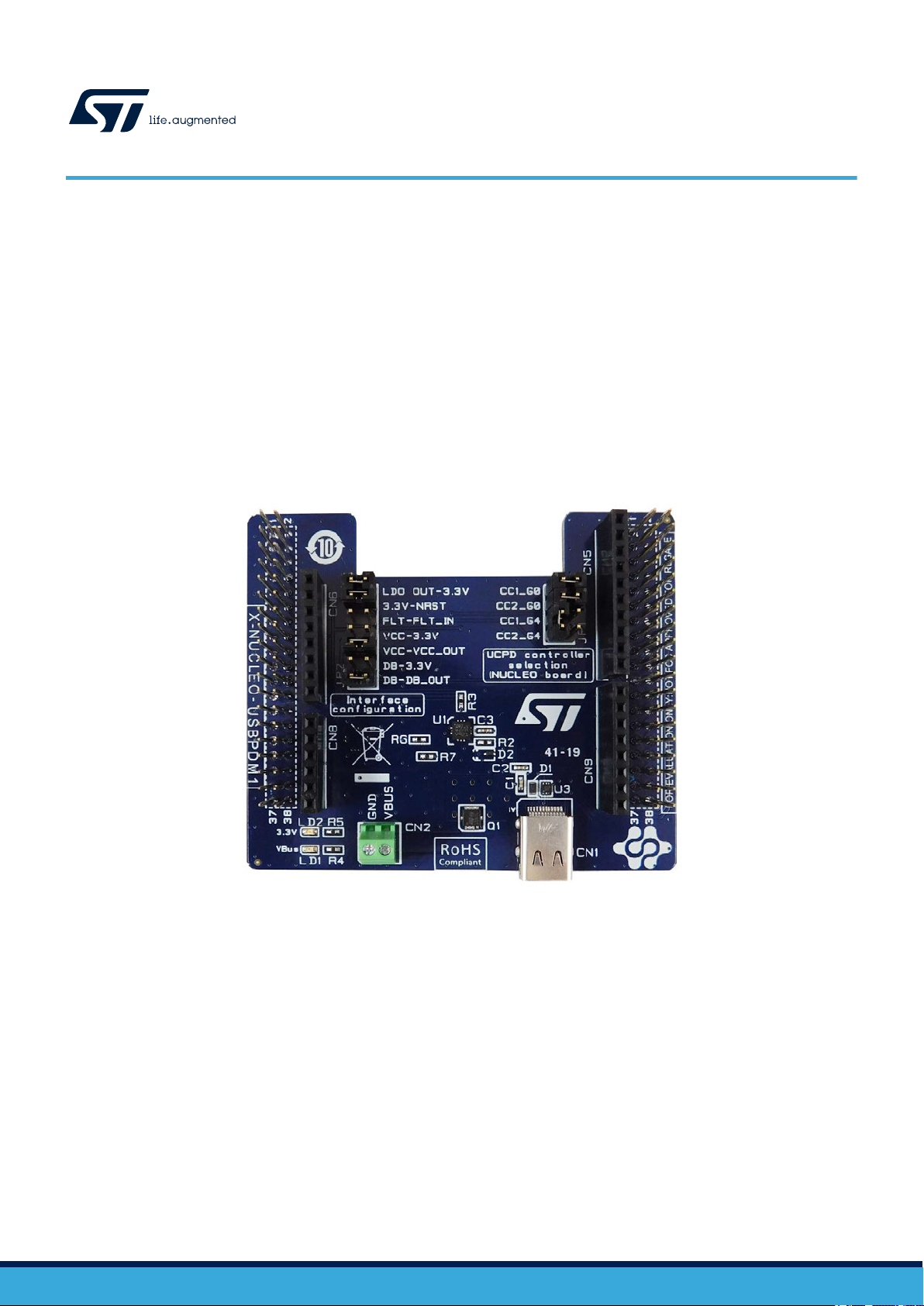
Getting started with the X-NUCLEO-USBPDM1 USB Type-C™ Power Delivery
Sink expansion board based on TCPP01-M12 for STM32 Nucleo
Introduction
The X-NUCLEO-USBPDM1 is an expansion board for the NUCLEO-G071RB and NUCLEO-G474RE development boards or
any STM32 Nucleo development board equipped with a USB Type-C peripheral.
The X-NUCLEO-USBPDM1 is compliant with USB Type-C Rev 1.2 and Power Delivery 3.0 with 100 W PPS support, as well as
USB-IF certified (Test ID certification: 3036).
It provides a straightforward means for evaluating USB Type-C Power Delivery in Sink mode based on TCPP01-M12.
The USB Type-C connector can supply the STM32 Nucleo development board thanks to a 3.3 V LDO.
Figure 1. X-NUCLEO-USBPDM1 expansion board
UM2668 - Rev 3 - April 2021
For further information contact your local STMicroelectronics sales office.
www.st.com
1 Getting started
1.1 Overview
The X-NUCLEO-USBPDM1 expansion board features:
• 100 W programmable power supply (PPS) support
• USB Type-C reversible connector
• 6 V overvoltage protection (OVP) on CC lines against short-to-V
• Up to 22 V adjustable overvoltage protection (OVP) on V
• Surge protection and system-level ESD protection on V
• Common-mode filter and ESD protection on USB 2.0 High Speed data-lines
• System-level ESD protection on CC lines as per IEC61000-4-2 level 4 (±8 kV contact discharge)
• Low power mode for battery operation allows zero current consumption when no cable is attached
• Integrated dead battery management for fully depleted battery devices
• Overtemperature protection (OTP)
• Compliant with USB Type-C Rev 1.2 and Power Delivery 3.0 standards
• USB-IF certified (Test ID certification: 3036)
when the connector is unplugged
BUS
line against charger failure
BUS
BUS
UM2668
Getting started
1.2 Hardware requirements
The X-NUCLEO-USBPDM1 expansion board is designed to be used with any STM32 Nucleo development board
equipped with a UCPD peripheral (for example, NUCLEO-G01xxxx or NUCLEO-G41xxxx), although complete
testing has only been performed using NUCLEO-G071RB and NUCLEO-G474RE development boards hosting
the STM32G071RB and STM32G474RE microcontrollers, respectively.
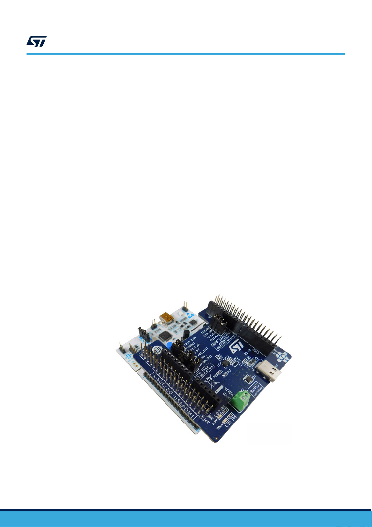
The expansion board must be plugged on the matching pins of the development board connector.
Figure 2. X-NUCLEO-USBPDM1 plugged on an STM32 Nucleo board
UM2668 - Rev 3
page 2/19

1.3 Software requirements
• All-in-one multi-OS software tool for programming STM32 products (STM32CubeProg)
• ST
• Binary files with specific use-cases (X-CUBE-TCPP)
-LINK/V2-1 USB driver
UM2668
Software requirements
UM2668 - Rev 3
page 3/19

UM2668
Board component description and configuration
2 Board component description and configuration
2.1 Connectors
The X-NUCLEO-USBPDM1 expansion board is equipped with USB T
V
can supply:
BUS
• the power connector (CN2) in normal mode
• STM32 when LDO (U2) output is connected to 3.3 V pin
2.2 Jumpers
To select the STM32 Nucleo development board to be used with the X-NUCLEO-USBPDM1 expansion board,
use JP1 jumper (UCPD peripheral selection) and CC lines (CC1 and CC2) connection:
•
For the NUCLEO-G071RB development board, use STM32 UCPD transceiver CC lines connection to ST
morpho connector (CN10–23 and CN10–26).
• For the NUCLEO-G474RE development board, use STM32 UCPD transceiver CC lines connection to ST
morpho connector (CN10–17 and CN10–27).
Other connections among the two boards are configured by JP2 jumpers.
The global jumper setup is the following:
• LDO OUT – 3.3 V to connect the LDO output to 3.3 V on the X-NUCLEO-USBPDM1. The STM32 is
powered by the USB Type-C connector.
Note: In this mode, the only way to program the STM32 Nucleo development board is to power the ST-LINK and
disconnect the LDO output.
• 3.3 V is common between X-NUCLEO-USBPDM1 and STM32 Nucleo development boards.
• 3.3 V – NRST to force the STM32 I/O negative reset to level ‘1’. It must be connected when the STM32
is powered by the X-NUCLEO-USBPDM1 and when the STM32 Nucleo development board ST-LINK
is connected. When programming or when ST-LINK is physically disconnected from the STM32 Nucleo
development board, 3.3 V – NRST must be disconnected.
• FLT – FLT_IN to connect the TCPP01-M12 fault report (open drain) to a pull-up output and to the ST
morpho connector (CN10 – 18, PC0 of NUCLEO-G071RB and PB11 of NUCLEO-G474RE).
The TCPP01-M12 supply options are:
• VCC – 3.3V to supply the TCPP01-M12 VCC with 3.3 V.
• VCC – VCC_OUT to supply the TCPP01-M12 VCC via a GPIO on ST morpho connector (CN7 – 1, PC10
of NUCLEO-G071RB and NUCLEO-G474RE). This case is useful with battery powered devices as the
TCPP01-M12 can be powered only when an attachment is detected (low power mode).
• Integrated dead battery management for fully depleted battery devices.
Dead battery management options are:
• DB – 3.3 V to remove the TCPP01-M12 dead battery clamp when 3.3 V is present.
• DB – DB_OUT to remove the TCPP01-M12 dead battery clamp when GPIO is connected on ST morpho
connector CN10 – 24. In this case, the STM32 MCU manages dead battery clamp removal.
ype-C™ connector (CN1).
2.3 LEDs
Two LEDs are mounted on the X-NUCLEO-USBPDM1 expansion board top side:
•
A red LED to indicate the USB Type-C V
• A green LED to indicate that 3.3 V is present and can be supplied by the STM32 Nucleo development board
or by the X-NUCLEO-USBPDM1 LDO.
UM2668 - Rev 3
voltage is present (voltage on CN2 and LDO powered).
BUS
page 4/19

UM2668
VBUS overvoltage protection setup
2.4 V
overvoltage protection setup
BUS
On the X-NUCLEO-USBPDM1 expansion board bottom side, a zero Ohm resistor (R0) selects a 22 V OVP
threshold.
o change the threshold to another value (6 V, 10 V, 13 V or 17 V), R0 must be removed and a solder bridge must
T
be added on the selected OVP voltage.
2.5 USB Type-C D+/D- connections
On the X-NUCLEO-USBPDM1 expansion board bottom side, D+/D- lines from USB Type-C CN1 are connected
to D+/D- lines of the NUCLEO-G474RE development board thanks to R8 and R9 zero Ohm resistors. These lines
can be used for USB BC 1.2 check and data transmission.
There is no USB data on the NUCLEO-G071RB but USB BC 1.2 check can be done thanks to STM32G071RB
PA4 (CN7 – 32) and PA5 (CN10 – 11): zero Ohm resistors R8 and R9 must be unsoldered and zero Ohm
resistors must be soldered on R10 and R11 footprints.
UM2668 - Rev 3
page 5/19
3 Programming and debugging
For programming and debugging, the X-NUCLEO-USBPDM1 expansion board must be powered by the STM32
Nucleo development board.
JP2 LDO OUT – 3.3 V and 3.3 V – NRST
TCPP01-M12 can be powered by one of the following options:
• the STM32 Nucleo 3.3 V (JP2 Vcc – 3.3 V jumper close and VCC – V_OUT jumper open)
• a dedicated STM32 GPIO for battery powered cases (JP2 VCC – 3.3V jumper open and VCC – V_OUT
jumper closed). This case is also called low power mode.
TCPP01-M12 dead battery resistor clamps are removed:
• automatically when 3.3 V is present (JP2 DB – 3.3 V jumper closed and DB – DB_OUT open)
• or by a GPIO (JP2 DB – 3.3 V jumper open and DB – DB_OUT closed)
pins must be removed.
UM2668
Programming and debugging
UM2668 - Rev 3
page 6/19

4 USB Type-C powered mode
UM2668
USB Type-C powered mode
Once STM32 is programmed, it is possible to power the STM32 using USB Type-C V
a source device connected to the T
ype-C connector (CN1). The X-NUCLEO-USBPDM1 on-board LDO (U2)
voltage through
BUS
generates 3.3 V to supply the system. In this case, 5 V is not available yet on the STM32 Nucleo development
board.
Note: STM32 Nucleo development board power jumper must not be connected (JP2 of NUCLEO-G071RB or JP5 of
NUCLEO-G474RE).
JP2 LDO OUT–3.3 V and 3.3 V–NRST jumpers must be closed.
TCPP01-M12 can be powered by:
• 3.3 V from the USB Type-C connector V
(JP2 Vcc – 3.3 V jumper closed and Vcc–V_OUT jumper open)
BUS
or
• a dedicated STM32 GPIO for battery powered cases (JP2 Vcc – 3.3 V jumper open and Vcc–V_OUT
jumper closed). This case is also called low power mode.
TCPP01-M12 dead battery resistor clamps are removed:
• automatically when 3.3 V is present (JP2 DB – 3.3 V jumper closed and DB – DB_OUT open) or
• by GPIO (JP2 DB – 3.3 V jumper open and DB – DB_OUT closed).
UM2668 - Rev 3
page 7/19

UM2668
NUCLEO-G474RE Type-C powered mode Sink contract negotiation
5 NUCLEO-G474RE Type-C powered mode Sink contract negotiation
In this case, dead battery clamps are removed when 3.3 V jumper is connected (not in low power mode).
NUCLEO-G474RE must be powered by ST
Step 1. Connect the NUCLEO-G474RE micro-USB connector (CN1) to your PC.
NUCLEO-G474RE appears as a virtual disk (NODE_G474RB).
Step 2. To program the STM32G474RE, drag and drop the binary file corresponding to the required voltage
(G474RE_TCPP01_no-low-power_no-DB-mng_SNK_xxV_v1.bin, xx is the selected voltage) to
the virtual disk.
LD1 blinks red and green for few seconds. When it does not blink any more, programming is complete.
Step 3. Plug the X-NUCLEO-USBPDM1 expansion board on top of the NUCLEO-G474RE development board.
Step 4. On X-NUCLEO-USBPDM1 JP1, close CC1_G4 and CC2_G4, and leave the other jumpers open.
Step 5. On X-NUCLEO-USBPDM1 JP2, close Vcc–3.3 V and DB–3.3V and leave the other jumpers open.
X-NUCLEO-USBPDM1 CN1 (USB Type-C receptacle) can be connected to any Type-C source. The
X-CUBE-TCPP selects the highest and closest power profile to the value indicated by the binary file
from available power profiles on the source. The obtained voltage can be measured on X-NUCLEO-
USBPDM1 CN2.
-LINK micro-USB connector (JP5 5V_STLK jumper closed).
Step 6. Disconnect the micro-USB cable from NUCLEO-G474RE CN1 and the USB Type-C cable from X-
NUCLEO-USBPDM1 CN1.
Step 7. Remove the power supply from NUCLEO-G474RE (JP5 fully open).
Step 8. On X-NUCLEO-USBPDM1 JP2, close LDO OUT 3.3 V, 3.3 V–NRST, Vcc–3.3 V and DB – 3.3 V and
leave the other jumpers open.
As previously mentioned, X-NUCLEO-USBPDM1 CN1 (USB Type-C receptacle) can be connected to
any Type-C source. The X-CUBE-TCPP selects the highest and closest power profile to the value
indicated by the binary file from available power profiles on the source. STM32G474RE is then
powered by Type-C connector and X-NUCLEO-USBPDM1 can be fine tuned with V
selection thanks to R0 position change. This configuration is relevant for a Type-C powered device
without battery as it is not in low power mode (Vcc is directly connected to 3.3 V). The data lines of
Type-C connector CN1 are connected to the STM32G474RE USB 2.0 full-speed transceiver thanks to
R8 and R9 zero Ohm resistors.
OVP voltage
BUS
UM2668 - Rev 3
page 8/19

UM2668
NUCLEO-G071RB Type-C powered mode Sink contract negotiation
6 NUCLEO-G071RB Type-C powered mode Sink contract negotiation
In this case, dead battery clamps are managed by STM32G071RB in low power mode.
NUCLEO-071RB must be powered by ST
Step 1. Connect the NUCLEO-071RB micro-USB connector (CN1) to your PC.
NUCLEO-071RB appears as a virtual disk (NODE_G071RB).
Step 2. To program the STM32G071RB, drag and drop the binary file corresponding to the required voltage
(G071RB_TCPP01_low-power_no-DB-mng_SNK_xxV_v1.bin, xx is the selected voltage) to the
virtual disk.
LD1 blinks red and green for few seconds. When it does not blink anymore, programming is complete.
Step 3. Plug the X-NUCLEO-USBPDM1 expansion board on top of the NUCLEO-071RB development board.
Step 4. On X-NUCLEO-USBPDM1 JP1, close CC1_G0 and CC2_G0, and leave the other jumpers open.
Step 5. On X-NUCLEO-USBPDM1 JP2, close Vcc–Vcc_OUT and DB-DB_OUT and leave the other jumpers
open.
X-NUCLEO-USBPDM1 CN1 (USB Type-C receptacle) can be connected to any Type-C source. The
X-CUBE-TCPP selects the highest and closest power profile to the value indicated by the binary file
from available power profiles on the source. The obtained voltage can be measured on X-NUCLEO-
USBPDM1 CN2.
-LINK micro-USB connector (JP2 STLK jumper closed).
Step 6. Disconnect the micro-USB cable from NUCLEO-071RB CN1 and the USB Type-C cable from X-
NUCLEO-USBPDM1 CN1.
Step 7. Remove the power supply from NUCLEO-071RB (JP2 fully open).
Step 8. On X-NUCLEO-USBPDM1 JP2, close LDO OUT 3.3 V, 3.3 V–NRST, Vcc–Vcc_OUT and DB-
DB_OUT and leave the other jumpers open.
As previously mentioned, X-NUCLEO-USBPDM1 CN1 (USB Type-C receptacle) can be connected to
any Type-C source. The X-CUBE-TCPP selects the highest and closest power profile to the value
indicated by the binary file from available power profiles on the source. STM32G474RE is then
powered by Type-C connector and X-NUCLEO-USBPDM1 can be fine tuned with V
selection thanks to R0 position change or via USB BC 1.2 check on source (short on D+/-) thanks to
R8 and R9 zero Ohm resistor position change to R10 and R11 positions.
This configuration is relevant for a battery-powered device thanks to the low power mode (Vcc
connected to GPIO). This results in zero power consumption for the TCPP01-M12 when the Type-C
cable is unplugged.
OVP voltage
BUS
UM2668 - Rev 3
page 9/19

7 Jumper tables
Jumper NUCLEO-G071RB selection NUCLEO-G474RE selection
CC1_G0
CC2_G0
CC1_G4
CC2_G4
UM2668
Jumper tables
Table 1. JP1 connector
Table 2. JP2 connector - low power mode
Jumper ST-LINK powered USB-Type-C powered
LDO OUT–3.3 V
3.3 V–NRST
FLT–FLT_IN
–3.3 V
V
CC
V
DB–DB_OUT
CC–VCC
DB–3.3 V
_OUT
Table 3. JP2 connector - no low power mode
Jumper ST-LINK powered USB-Type-C powered
LDO OUT–3.3 V
3.3 V–NRST
FLT–FLT_IN
–3.3 V
V
CC
V
DB–DB_OUT
CC–VCC
DB–3.3 V
_OUT
USB-Type-C powered
ST-LINK removed
USB-Type-C powered
ST-LINK removed
UM2668 - Rev 3
page 10/19

6
32
5
3334
CN7
2
8
3
FB
GND
11
10
UCPD Controller Selection
9
CC1_G0
8
CN5
7
7
CC2_G0
3
6
DB_OUT
2
38
1
36
37
VCC_OUT
(
(
4
6
6
5
5
OUT
4
EP
C6
470nF
DB/
1
LDO_OUT
2
9
10
6
CC1_G4
C5
5
100nF
CC1
1
JP1
3
200K
8
2
ADC_VBUS
4
DB_OUT
3
CC2_G4
2
CC1_G4
R6
25
FLT_IN
26
27
3
25
5
2324
Interface Configuration
4
CC2_G0
2
VCC
3
NC
NC
GND
19
8
GND
FLT
5
20
DP_G4
1
CN6
VBUS
22
21
28
CC2
4
DM_G4
GND
1
29
18
28
NC
NC
16
17
PA5_G0
18
19
11
R7
3.3V
LDO_OUT
ADC_VBUS
4
7
31
5
15
30
6
1314
12
32
40.2K
ST715PU33R
3.3V
VBUS
21
20
IN
CN10
38
22
12
FLT_IN
11
CN9
3
8
GND
4
7
CN8
10
GND
U2
2324
3
2
9
26
27
CC2_G4
5
6
VCC_OUT
4
1314
36
37
3
JP2
NRST
35
NRST
12
7
1314
6
7
5
CC1_G0
8
2
7
31
4
1
30
9
29
1
8
1
PA4_G0
2
7
1
6
15
16
17
10
3334
9
35
8
UM2668 - Rev 3
8 Schematic diagrams
Figure 3. X-NUCLEO-USBPDM1 circuit schematic (1 of 2)
page 11/19
Schematic diagrams
UM2668

3.3V
7
A12
13V
6
VCC
R1D
0R
A10
SSRXn2
SSRXp2
1
A11
PA5_G0
CC1
MPT 0.5/2-2.54
Dp1
Dn1
2
R8
CN1
DP
R2
25
0R
B12
0R
SSRXn1
SSRXp1
2
VBUS
100W
GND
A9
LD1
RED
1
31
R1E
30
VBUS
29
Q1
STL11N3LLH6
10K
GND
620R
R9
GND
VBUS
VBUS
4
PA4_G0
3
32
GND
GND
B5
GATE
DB\
D
FLT
VCC
27W
S
M4
LD2
5
SENSE
CC1c
VBUS
VBus max
SH4
3
4
CC1c
5
USB_TypeC_Receptacle
6
GATE
DM
D+
R0
VBUS_CTRL
10V
SH3
VBUS
B1
DB/
CC2
B2
D1
15W
CC2c
IN_GD
1.5K
3.3V
GND
D2
GREEN
P max
M1
VBUSc
CC2
Fiducial on board
2
22V
1
U1
EP
VBus
CC1
GND
SOURCE
0R
Dp2
Dn2
B11
B10
B9
SBU2
CC2c
10K
R3
SH1
GND
GNDGND
17V
GND
100nF
VBus
GND
CN2
GND
TCPP01-M12
CC2
CC1
13
B6
B7
330pF
36W
B8
C1
R1B
1.0K
R5
GND
R10
D-
R1C
VBUS
CC2c
C3
R11
11
SSTXp2
SSTXn2
45W
12
U3
GND
1.1K
ECMF02-2AMX6
0R
ESDA25P35-1U1M
B3
B4
A6
A7
A1
632723300011
A5
DP_G4
GND
DM_G4
D+
FLT
C2
D-
330pF
NC
6V
820R
VBUSc
BAT54KFILM
SBU1
GND
9
CC1c
ZDiff 90 Ohm
8
R4
G
10
A3
A4
A2
SSTXp1
SSTXn1
A8
VBUSc
M2
GND
VBUS
SH2
M3
2.7K
4K
R1A
28
Mid PINMid PIN
26
27
ZDiff 90 Ohm
UM2668 - Rev 3
Figure 4. X-NUCLEO-USBPDM1 circuit schematic (2 of 2)
page 12/19
Schematic diagrams
UM2668

9 Bill of materials
Item Q.ty Ref. Part/Value Description Manufacturer Order code
1 1 CN1
2 1 CN2
3 2 CN7, CN10
4 1 CN5
5 2 CN6, CN9
6 1 CN8
7 2 C1, C2
8 2 C3, C5
9 1 C6
10 5 R0, R8, R9 SMD 0, 0402 Resistors Any Any
11 1 R1_6V
12 1 R1_10V
13 1 R1_13V
14 1 R1_17V
15 1 R1_22V
16 2 R2, R3
17 1 R4
18 1 R5
19 1 R6
20 1 R7
Table 4. X-NUCLEO-USBPDM1 bill of materials
USB_TypeC_Rec
eptacle
Through-hole,
2x1, 2.54 mm
pitch
Strip 19x2, 2.54
mm pitch
10 pins, 2.54 mm
pitch
11 pins, 2.54 mm
pitch
12 pins, 2.54 mm
pitch
330 pF, SMD
0402, X7R, 50
Vdc
100 nF, SMD
0402, X7R, 50
Vdc
470 nF, SMD
0402, X5C, 6 Vdc
2.7 k, SMD,
0402, 1/4 W
1.5 K, SMD, 0402
±1%
1.1 k, SMD, 0402
±1%
820, SMD, 0402 ,
1/4 W ±1%
620 SSMD 620,
1, 0402 Resistor
620 1% 0402
10 k, SMD 10k,
1, 0402 K 1%
0402
4 k, SMD 4k, 1,
0402 K 1% 0402
1 k, SMD 1k, 1,
0402 K 1% 0402
40 k, SMD 40,
2k, 1, 0402 K 1%
0402
200 k, SMD
200k, 1, 0402 K
1% 0402
Type-C
connector
Screw
connector
ST morpho
connector
Arduino UNO
R3 connector
Arduino UNO
R3 connector
Arduino UNO
R3 connector
Multilayer
ceramic
capacitors
Multilayer
ceramic
capacitors
Multilayer
ceramic
capacitors
Resistor Any Any
, ±1%
Resistor Any Any
Resistor Any Any
Resistor Any Any
Resistor Any Any
Resistor Any Any
Resistor Any Any
Resistor Any Any
Resistor Any Any
Resistor Any Any
Wurth
Electronics Inc.
Wurth
Electronics Inc.
SAMTEC ESQ-119-24-T-D
Wurth
Electronics Inc.
Wurth
Electronics Inc.
Wurth
Electronics Inc.
Wurth
Electronics Inc.
Any Any
Any Any
UM2668
Bill of materials
632723300011
691210910002
61301011821
61300811821
61300611821
885012205058
UM2668 - Rev 3
page 13/19

Item Q.ty Ref. Part/Value Description Manufacturer Order code
21 1 LD1 SMD 0603 Red LED
22 1 LD2 SMD 0603 Green LED
23 1 Q1
24 1 D1 25 V, 35 A
25 1 D2
26 1 U1 µQFN
27 1 U2
28 1 U3 QFN-6L
29 1 JP1 2.54 mm 2x4 Jumper
30 1 JP2 2.54 mm 2x7 Jumper
31 7 2.54 mm Header
30 V, 11 A,
PowerFLA
3.3
300 mA, 40 V,
SOD523
24 V, 4 V, 85 mA,
DFN8
T 3.3 x
N-channel 30 V,
6 mOhm typ., 11
A STripFET H6
Power MOSFET
High-power
transient voltage
suppressor
(TVS)
General
purpose signal
Schottky diode
USB Type-C
port protection
High input
voltage LDO
linear regulator
Common-mode
filter and ESD
protection for
USB 2.0 and
MIPI/MDDI
interfaces
Wurth
Electronics Inc.
Wurth
Electronics Inc.
ST STL11N3LLH6
ST ESDA25P35-1U1M
ST BAT54KFILM
ST TCPP01-M12
ST ST715PU33R
ST ECMF02-2AMX6
Wurth
Electronics Inc.
Wurth
Electronics Inc.
Wurth
Electronics Inc.
150060RS75000
150060GS75000
61300821121
61301421121
61300711121
UM2668
Bill of materials
UM2668 - Rev 3
page 14/19

Revision history
17-Dec-2019 1 Initial release.
14-May-2020 2 Updated Introduction and Section 1.1 Overview.
06-Apr-2021 3 Replaced X-CUBE-USBPDM1 with X-CUBE-TCPP.
UM2668
Table 5. Document revision history
Date Version Changes
UM2668 - Rev 3
page 15/19

UM2668
Contents
Contents
1 Getting started ....................................................................2
1.1 Overview .....................................................................2
1.2 Hardware requirements .........................................................2
1.3 Software requirements ..........................................................3
2 Board component description and configuration ...................................4
2.1 Connectors....................................................................4
2.2 Jumpers ......................................................................4
2.3 LEDs .........................................................................4
2.4 V
2.5 USB T
overvoltage protection setup ................................................5
BUS
ype-C D+/D- connections ..................................................5
3 Programming and debugging ......................................................6
4 USB Type-C powered mode ........................................................7
5 NUCLEO-G474RE Type-C powered mode Sink contract negotiation.................8
6 NUCLEO-G071RB Type-C powered mode Sink contract negotiation.................9
7 Jumper tables ....................................................................10
8 Schematic diagrams ..............................................................11
9 Bill of materials...................................................................13
Revision history .......................................................................15
UM2668 - Rev 3
page 16/19

UM2668
List of tables
List of tables
T
able 1. JP1 connector .....................................................................10
Table 2. JP2 connector - low power mode ........................................................10
Table 3. JP2 connector - no low power mode...................................................... 10
Table 4. X-NUCLEO-USBPDM1 bill of materials.................................................... 13
Table 5. Document revision history ............................................................. 15
UM2668 - Rev 3
page 17/19

UM2668
List of figures
List of figures
Figure 1. X-NUCLEO-USBPDM1 expansion board ..................................................1
Figure 2. X-NUCLEO-USBPDM1 plugged on an STM32 Nucleo board ....................................2
Figure 3. X-NUCLEO-USBPDM1 circuit schematic (1 of 2) ........................................... 1
Figure 4. X-NUCLEO-USBPDM1 circuit schematic (2 of 2) ........................................... 12
1
UM2668 - Rev 3
page 18/19

UM2668
IMPORTANT NOTICE – PLEASE READ CAREFULLY
STMicroelectronics NV and its subsidiaries (“ST”) reserve the right to make changes, corrections, enhancements, modifications, and improvements to ST
products and/or to this document at any time without notice. Purchasers should obtain the latest relevant information on ST products before placing orders. ST
products are sold pursuant to ST’
Purchasers are solely responsible for the choice, selection, and use of ST products and ST assumes no liability for application assistance or the design of
Purchasers’ products.
No license, express or implied, to any intellectual property right is granted by ST herein.
Resale of ST products with provisions different from the information set forth herein shall void any warranty granted by ST for such product.
ST and the ST logo are trademarks of ST. For additional information about ST trademarks, please refer to www
names are the property of their respective owners.
Information in this document supersedes and replaces information previously supplied in any prior versions of this document.
s terms and conditions of sale in place at the time of order acknowledgement.
.st.com/trademarks. All other product or service
© 2021 STMicroelectronics – All rights reserved
UM2668 - Rev 3
page 19/19
 Loading...