

Datasheet USB1T11AMX, USB1T11AMTCX, USB1T11AMTC, USB1T11AM Datasheet (Fairchild Semiconductor)
Page 1
USB1T11A
Universal Serial Bus Transceiver
USB1T11A Universal Serial Bus Transceiver
November 1999
Revised December 1999
General Description
The USB1T11A is a one chip generic USB transceiver. It is
designed to allow 5.0V or 3.3V programmable and standard logic to interfac e with the physical layer of the Univ e rsal Serial Bus. It is c apable of transmitting an d receiving
serial data at both full speed (12Mbit/s) and low speed
(1.5Mbit/s) data rates.
The input and output signals of the USB1T11A conform
with the “Serial Inter face Engine”. Implementation of the
Serial Interface Engine along with the USB1T11A allows
the designer to make USB c omp atib l e de vices wi t h off-th eshelf logic and easily modify and update the application.
Features
■ Complies with Universal Serial Bus specification 1.1
■ Utilizes digital inputs and outputs to transmit and receive
USB cable data
■ Supports 12Mbit/s “Full Speed” and 1.5Mbit/s “Low
Speed” serial data transmission
■ Compatible with the VHDL “Serial Interface Engine” from
USB Implementers’ Forum
■ Supports single-ended data interface
■ Single 3. 3V supply
■ ESD Performance : Human Body Model > 4000 V
Ordering Code:
Order Number Package Number Package Description
USB1T11AM M14A 14-Lead Small Outline Integrated Circuit (SOIC), JEDEC MS-012, 0.150” Narrow
USB1T1 1AMTC MTC14 14-Lead Thin Shrink Small Outline Package (TSSOP), JEDEC MO-153, 4.4mm Wide
Device also available in Tape and Reel. Specify by appending suffix letter “X” to the ordering code.
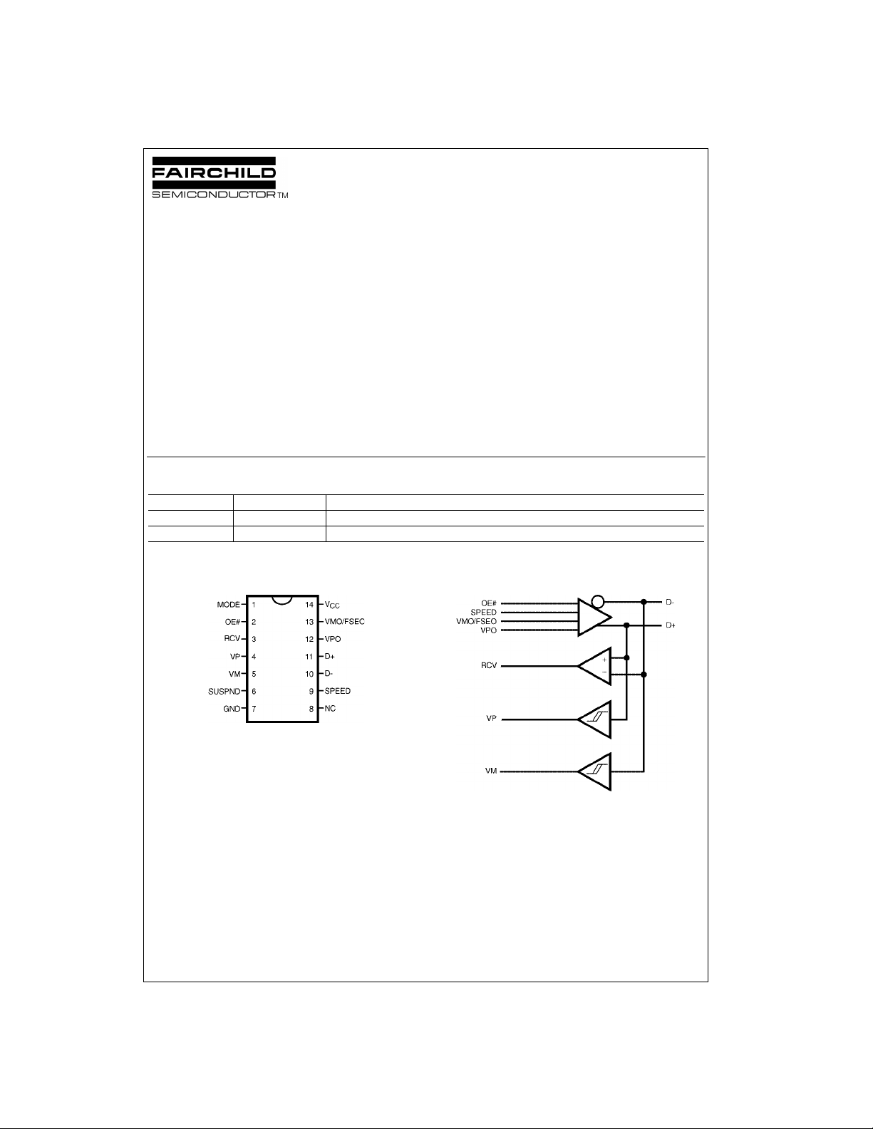
Connection Diagram Logic Diagram
© 1999 Fairchild Semiconductor Corporation DS500234 www.fairchildsemi.com
Page 2
Pin Descriptions
Pin Name I/O Description
RCV O Receive data. CMOS level output for USB differential input
USB1T11A
OE# I
MODE I
, VMO/F
V
PO
SEO
V
, V
P
M
D+, D− AI/O Data+, Data−. Differential data bus conforming to the Universal Serial Bus standard.
SUSPND I
SPEED I
V
CC
GND Ground reference
Output Enable. Active LOW, enables the transceiver to transmit data on the bus. When not
active the transceiver is in receive mode.
Mode. When left unconnected, a weak pull-up transistor pulls it to V
VMO/FSEO pin takes the function of FSEO (Force SEO).
Inputs to differential driver. (Outputs from SIE).
MODE VPO VMO/FSEO RESULT
0 0 0 Logic “0”
01 SE0#
I
1 0 Logic “1”
1 1 SEO#
10 0 SE0#
0 1 Logic “0”
1 0 Logic “1”
1 1 Illegal code
Gated version of D− and D+. Outputs are logic “0” and logic “1”. Used to detect single ended
zero (SE0#), error conditions, and interconnect speed. (Input to SIE).
VP VM RESULT
O
0 0 SE0#
0 1 Low Speed
1 0 Full Speed
11Error
Suspend. Enables a low power state while the USB bus is inactive. While the suspend pin is
active it will drive the RCV pin to a logic “0” state. Both D+ and D− are 3-STATE.
Edge rate control. Logic “1” operates at edge rates for “full speed”.
Logic “0” operates edge rates for “low speed”.
3.0V to 3.6V power supply
and in this GND, the
CC
Functional Truth Table
Input I/O Outputs
Mode VPO VMO/FSEO OE SUSPND D+ D− RCV
V
0 0 0 0 0 0 1 0 0 1 Logic 0
0 0 1 0 0 0 0 U 0 0 SEO#
0 1 0 0 0 1 0 1 1 0 Logic 1
0 1 1 0 0 0 0 U 0 0 SEO#
1 0 0 0 0 0 0 U 0 0 SEO#
1 0 1 0 0 0 1 0 0 1 Logic 0
1 1 0 0 0 1 0 1 1 0 Logic 1
1 1 1 0 0 1 1 U U U Illegal Code
X X X 1 0 ZZUUUD+/D− Hi-Z
X X X 1 1 ZZUUUD+/D− Hi-Z
X = Don’t Care
Z = 3-STATE
U = Undefined State
www.fairchildsemi.com 2
V
P
M
Result
Page 3
Absolute Maximum Ratings(Note 1) Recommended Operating
DC Supply Voltage (VCC) −0.5V to +7.0V
DC Input Diode Current (I
V
< 0 −50 mA
I
Input Voltage (V
)
I
)
IK
(Note 2) −0.5V to +5.5V
Input Voltage (V
Output Diode Current (I
V
> VCC or VO < 0 ±50 mA
O
Output Voltage (V
(Note 2) −0.5V to V
Output Source or Sink Current (I
) −0.5V to VCC + 0.5V
I/O
)
OK
)
O
)
O
CC
+ 0.5V
VP.VM, RCV pins
V
= 0 to V
O
CC
Output Source or Sink Current (I
)
O
±15 mA
D+/D− pins
= 0 to V
V
O
V
CC
CC
or GND Current (ICC, I
Storage Temperature (T
) ±100 mA
GND
) −60°C to + 150°C
STO
±50 mA
Conditions
Supply Voltage V
Input Voltage (V
Input Range for AI/O (V
Output Voltage (VO)0V to V
Operating Ambient Temperature
in free air (T
Note 1: The Absolute Maxi mum Ratings are thos e values beyond which
the safety of the d evice cannot b e guaranteed . The device sh ould not be
operated at these limit s. The parametric values defi ned in the Electrical
Characteristic tables are not guaranteed at the absolute maximum rating.
The “Recomm ended O peratin g Cond itions ” table will defin e the condition s
for actual device operation.
Note 2: The input and output voltage ratings may be exceeded if the input
and output clamp current ratings are observed.
CC
) 0V to 5.5V
I
amb
)0V to V
AI/O
) −40°C to +85°C
DC Electrical Characteristics (Digital Pins)
Over recommended range of supply voltage and operating free air temperature (unless otherwise noted). VCC = 3.0V to 3.6V
Symbol Parameter Test Conditions
Min Typ Max
CC
V
V
V
V
I
L
I
CCFS
I
CCLS
I
CCQ
I
CCS
INPUT LEVELS:
IL
IH
OL
OH
LOW Level Input Voltage 0.8 V
HIGH Level Input Voltage 2.0 V
OUTPUT LEVELS:
LOW Level Output Voltage IOL = 4 mA 0.4
HIGH Level Output Voltage IOH = 4 mA 2.4
LEAKAGE CURRENT:
Input Leakage Current VCC = 3.0 to 3.6 ±5 µA
Supply Current (Full Speed) VCC = 3.0 to 3.6 5 mA
Supply Current (Low Speed) VCC = 3.0 to 3.6 5 mA
Quiescent Current VCC = 3.0 to 3.6
Supply Current in Suspend VCC = 3.0 to 3.6; Mode = V
IOL = 20 µA0.1
= 20 µAV
I
OH
VIN = VCC or GND
CC
Limits
– 0.1
USB1T11A
3.0V to 3.6V
CC
CC
UnitTemp = −40°C to +85°C
V
V
5mA
10 µA
3 www.fairchildsemi.com
Page 4

DC Electrical Characteristics (D+/D− Pins)
Over recommended range of supply voltage and operating free air temperature (unless otherwise noted). VCC = 3.0V to 3.6V
Symbol Parameter Test Conditions
USB1T11A
Min Typ Max
INPUT LEVELS:
V
DI
V
CM
V
SE
Differential Input Sensitivity |(D+) – (D−)| 0.2 V
Differential Common Mode Range Includes VDI Range 0.8 2.5 V
Single Ended Receiver Threshold 0.8 2.0 V
OUTPUT LEVELS:
V
OL
V
OH
V
CR
Static Output LOW Voltage RL of 1.5 kΩ to 3.6V 0.3 V
Static Output HIGH Voltage RL of 15 kΩ to GND 2.8 3.6 V
Differential Crossover 1.3 2.0 V
LEAKAGE CURRENT:
I
OZ
High Z State Data Line Leakage Current 0V < VIN < 3.3V ±5 µA
CAPACITANCE:
CIN(Note 4) Transceiver Capacitance Pin to GND 10 pF
Capacitance Match 10 %
OUTPUT RESISTANCE:
Z
(Note 3) Driver Output Resistance Steady State Drive 4 20 Ω
DRV
Resistance Match 10 %
Note 3: Excludes external resistor. In order to comply with USB Specification 1.1, external series resistors of 24Ω ± 1% ea ch on D+ and D− are recom-
mended. This spec if ication is guarante ed by design and statis ti c al process distributio n.
Note 4: This specification is gu aranteed by design and statistical proces s distribution.
Limits
AC Electrical Characteristics (D+/D− Pins, Full Speed)
Over recommended range of supply voltage and operating free air temperature (unless otherwise noted). VCC = 3.0V to 3.6V
CL = 50 pF; RL = 1.5 kΩ on D+ to V
Symbol Parameter Test Condition
DRIVER CHARACTERISTICS:
t
t
V
R
F
RFM
CRS
Rise Time Figure 1 4 20
Fall Time Figure 1 4 20
Rise/Fall Time Matching (tr/tf)90110%
Output Signal Crossover Voltage 1.3 2.0 V
DRIVER TIMINGS:
t
PLH
t
PLH
t
PHZ
t
PLZ
t
PZH
t
PZL
Driver Propagation Delay Figure 2 18 ns
(VPO, VMO/FSEO to D+/D−) Figure 2 18ns
Driver Disable Delay Figure 4 13 ns
(OE# to D+/D−) Figure 4 13ns
Driver Enable Delay Figure 4 17 ns
(OE# to D+/D−) Figure 4 17ns
RECEIVER TIMINGS:
t
PLH
t
PHL
t
PLH
t
PHL
Receiver Propagation Delay Figure 3 16 ns
(D+, D− to RCV) Figure 3 19 ns
Single-ended Receiver Delay Figure 3 8 ns
(D+, D− to VP, VM) Figure 3 8 ns
CC
Limits
Min Typ Max
10% and 90%
UnitsTemp = −40°C to +85°C
UnitsTemp = −40°C to +85°C
nst
www.fairchildsemi.com 4
Page 5

AC Electrical Characteristics (D+/D− Pins, Low Speed)
Over recommended range of supply voltage and operating free air temperature (unless otherwise noted). VCC = 3.0V to 3.6V
CL = 200 to 600 pF; RL = 1.5k on D− to V
Symbol Parameter Test Conditions
DRIVER CHARACTERISTICS:
CC
Limits
T
= −40°C to +85°C
amb
Min Typ Max
USB1T11A
Unit
t
t
V
t
t
t
t
t
t
t
t
t
t
LR
LF
RFM
CRS
PLH
PHL
PHZ
PLZ
PZH
PZL
PLH
PHL
PLH
PHL
10% and 90%
Rise Time Figure 1 75 300
nst
Fall Time Figure 1 75 300
Rise/Fall Time Matching (tr/tf)80120%
Output Signal Crossover Voltage 1.3 2.0 V
DRIVER TIMINGS:
Driver Propagation Delay Figure 2 300 ns
(VPO, VMO/FSEO to D+/D−) Figure 2 300 ns
Driver Disable Delay Figure 4 13 ns
(OE# to D+/D−) Figure 4 13ns
Driver Enable Delay Figure 4 205 ns
(OE# to D+/D−) Figure 4 205 ns
RECEIVER TIMINGS:
Receiver Propagation Delay Figure 3 18 ns
(D+, D− to RCV) Figure 3 18 ns
Single-ended Receiver Delay Figure 3 28 ns
(D+, D− to VP, VM) Figure 3 28 ns
5 www.fairchildsemi.com
Page 6

AC Waveforms
VOL and VOH are the typical output voltage drops that occur with the output load. (VCC never goes below 3.0V)
USB1T11A
FIGURE 1. Rise and Fall Times
FIGURE 2. VPI, VMO/FSEO to D+/D−
FIGURE 3. D+/D− to RCV, VP/VM
Test Circuits and Waveforms
Load for VM/VP and RCV
CL = 50 pF, Full Speed
CL = 50 pFm Low Speed (Min Timing)
CL = 350 pF, Low Speed (Max Timing)
1.5 kΩ on D− (Low Speed) or D+ (Full Speed) only
Note:
V = 0 for t
V = VCC for t
Load for D+/D−
FIGURE 4. OE# to D+/D−
Load for Enable and Disable Times
, t
PZH
PHZ
, t
PZL
PLZ
Test S1
D−/LS Close
D+/LS Open
D−/FS Open
D+/FS Close
www.fairchildsemi.com 6
Page 7

Physical Dimensions inches (millimeters) unless otherwise noted
USB1T11A
14-Lead Small Outline Integrated Circuit (SOIC), JEDEC MS-012, 0.150” Narrow
Package Number M14A
7 www.fairchildsemi.com
Page 8

Physical Dimensions inches (millimeters) unless otherwise noted (Continued)
USB1T1 1A Universal Serial Bus T ransceiver
14-Lead Thin Shrink Small Outline Package (TSSOP), JEDEC MO-153, 4.4mm Wide
Fairchild does not assume any responsibility for use of any circuitr y described, no circuit patent licenses are implied a nd
Fairchild reserves the right at any time without notice to change said circuitry and specifications.
LIFE SUPPORT POLICY
FAIRCHILD’S PRODUCTS ARE NOT AUTHORIZED FOR USE AS CRITICAL COMPONENTS IN LIFE SUPPORT
DEVICES OR SYSTEMS WITHOUT THE EXPRESS WRITTEN APPROVAL OF THE PRESIDENT OF FAIRCHILD
SEMICONDUCTOR CORPORATION. As used herein:
1. Life support devices or systems a re devices or syste ms
which, (a) are intended for surgical implant into the
body, or (b) support or sustain life, and (c) whose failure
to perform when properly used in accordance with
instructions for use provided in the labeling, can be reasonably expected to result in a significant inju ry to the
user.
www.fairchildsemi.com 8
Package Number MTC14
2. A critical component in any com ponen t of a life su pport
device or system whose failu re to perform can be reasonably expected to cause the failure of the li fe su pp ort
device or system, or to affect its safety or effectiveness.
www.fairchildsemi.com
 Loading...