

Page 1
查询USB1101供应商
June 2005
Revised June 2005
USB1101
USB 2.0 FS Peripheral Transceiver (Preliminary)
General Description
The USB1101 provides a USB FS Transceiver functionality
with voltage level translation that is compliant to USB Specification Rev 2.0. The device allows interfacing of USB
Application specific devices with supply voltages ranging
from 1.65V to 3.6V with the physical layer of Universal
Serial Bus. It is capable of operating at 12Mbits/s (full
speed) data rates and hence is fully compliant to USB
Specification Rev 2.0. It supports the DAT_VP/SE0_VM
interface on the host side but offers reduced pin cou nt and
package size. The USB1101 has host side supply rail for
1.65V to 3.6V.
Features
■ Complies with USB Specification Rev 2.0
■ Supports DAT_VP/SE0_VM host mode
■ Utilizes digital inputs and outputs to transmit and receive
USB cable data
■ Supports full speed (12Mbits/s) data rates
■ Ideal for portable electronic devices
■ MicroPak
■ Host side V
¥
1.6mm x 2.1mm
technology package ( 10 pin)
CCIO
1.65V to 3.6V
Applications
•PDA
• PC Peripherals
• Cellular Phones
•MP3 Players
• Digital Cameras
• Information Appliance
Preliminary
USB1101 USB 2.0 FS Peripheral Transceiver (Preliminary)
Ordering Code:
Order Package Package
Number Number Top Mark
USB1101L10X MAC010A UB 10-Lead MicroPak, 1.6 mm x 2.1mm 5k Units on Tape and Reel
Package Description Supplied As
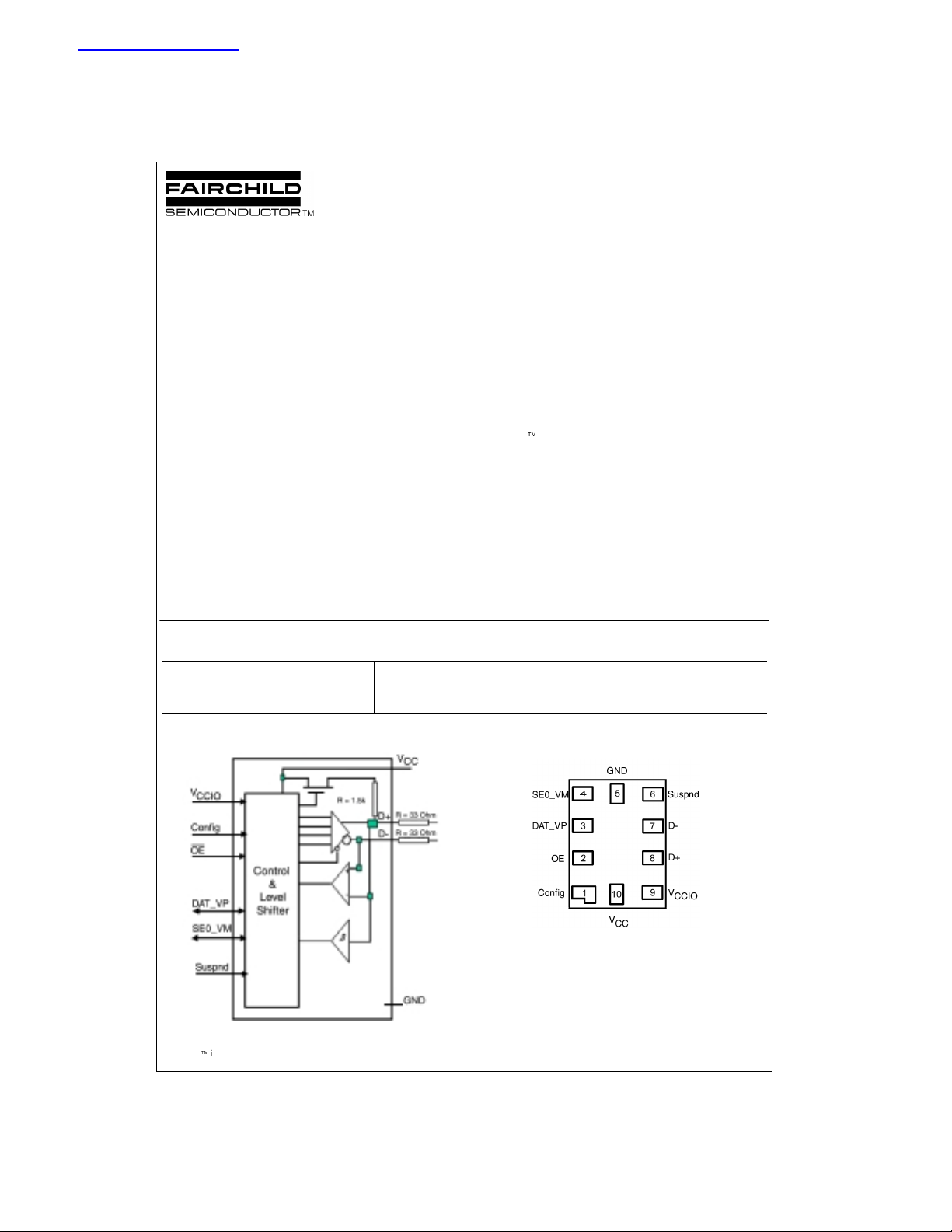
Connection Diagram
(Bottom View)
MicroPak¥ is a trademark of Fair ch ild Semiconductor Co rporation.
© 2005 Fairchild Semiconductor Corporation DS500923 www.fairchildsemi.com
Page 2
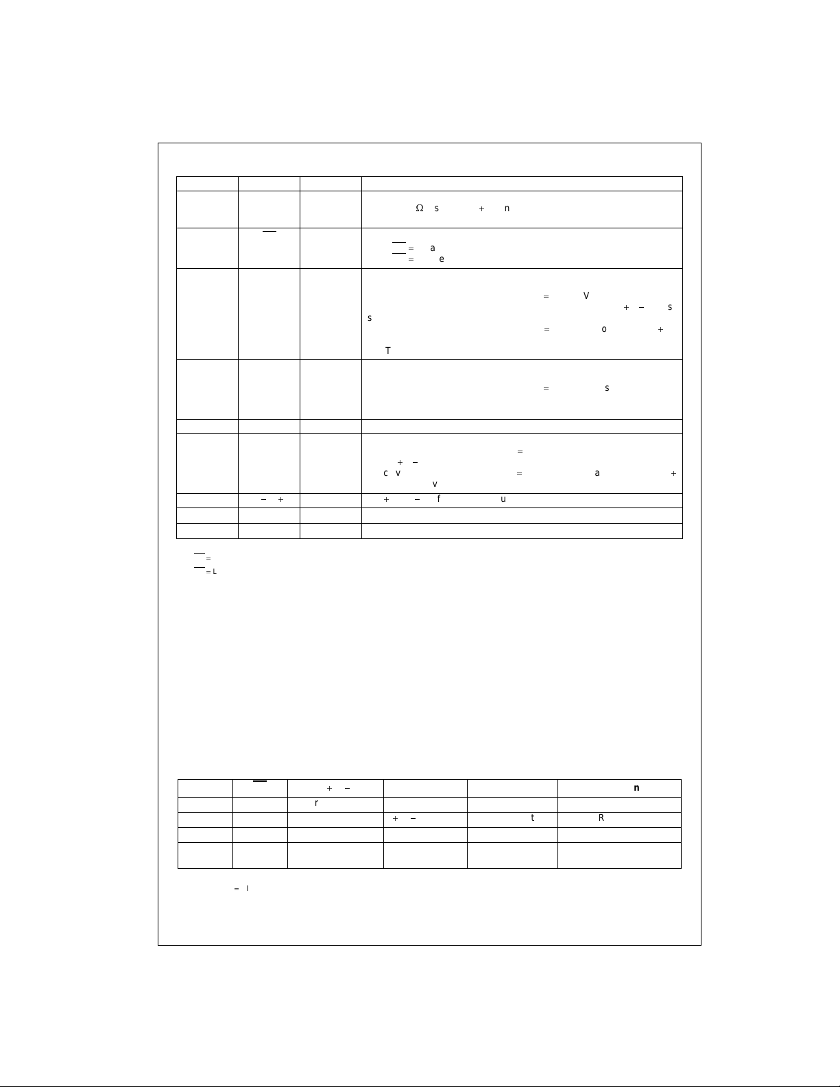
Pin Description
Pin Number Pin Name I/O Pin Description
USB1101
1 Config I USB connect or disconnect software control input. Configures 3.3V to
:
internal 1.5k
port then this pin is hard-wired to GND.
2OE
I Output Enable (active LOW)
When OE
When OE
3 DAT_VP I/O When in transmit mode
(CMOS level relative to V
When in receive mode
data output comprised of the differential input data from the D
(see Table 2);
When in receive mode
data.
(see Table 1 and Table 2) Output drive is 2mA (min) buffer
4 SE0_VM I/O When in transmit mode
tive to V
When in receive mode
resistor on D when HIGH. If device is used as Downstream
L transmit mode is enabled
H receive mode (CMOS level is relative to V
(Note 2)
CCIO
(Note 1)
(Note 1)
(Note 2)
).
CCIO
(Note 1)
put (see Table 2)
(see Table 1 and Table 2). Output drive is 4ma (min) buffer
5 GND GND GND
6 Suspnd I Enables a low power state (CMOS level is relative to V
In receive mode
of the D
In receive mode
/D
lines.
(Note 1)
with Suspnd L the DAT_VP pin will be a function
(Note 1)
with Suspnd H DAT_VP will have the value of D
such that the device can still monitor out-of-suspend signaling.
, D
7, 8 D
9V
10 V
CCIO
CC
AI/O Data, Data. Differential data bus conforming to the USB standard
Pwr Supply Voltage for host side digital I/O pins (1.65V to 3.6V)
Pwr Supply Voltage Input (3.0V to 3.6V)
Preliminary
) is enabled.
DAT_VP is a single-ended host data input
).
and Suspnd L DAT_VP is a single ended
with Suspnd H DAT_VP outputs the D
SE0_VM is a data input (CMOS level rela-
and Suspnd L, SE0_VM is used as an out-
CCIO
CCIO
/D
inputs
).
Note 1: OE H
Note 2: OE
L
Functional Description
The USB1101 transceiver is designed as an Upstream facing port device to convert CMOS d ata into US B differen tial
bus signal levels and to co nve rt USB differe ntial b us si gn al
to CMOS data. If you wish to use these as downstream
devices, Config must be hard-wired to GND.
To minimize EMI and noise the outputs are edge rate controlled with the rise and fall times controlled and defined for
full speed data rates only (12Mbits/s). The rise and fall
times are balanced between the differential pins to minimize skew.
TABLE 1. Function Select
Suspnd OE D, D
L L Transmitting Host Data Input SE0_VM Host Input Normal Driving
L H Receiving (Note 3) D
H L Transmitting (Note 4) Host Data Input SE0_VM Host Input Driving while Suspended
H H Driver is 3-STATE
DAT_VP Output SE0_VM Output Suspended
(Note 4)
Note 3: Signal levels is functio n of c onnection, Config and/or pull-up/pull-down resistors.
Note 4: For Suspnd
HIGH mode the differential receiver is inactive.
The USB1101 supports the DAT_VP/SE0_VM format from
the OTG Transceiver Specification using the DAT_SE0
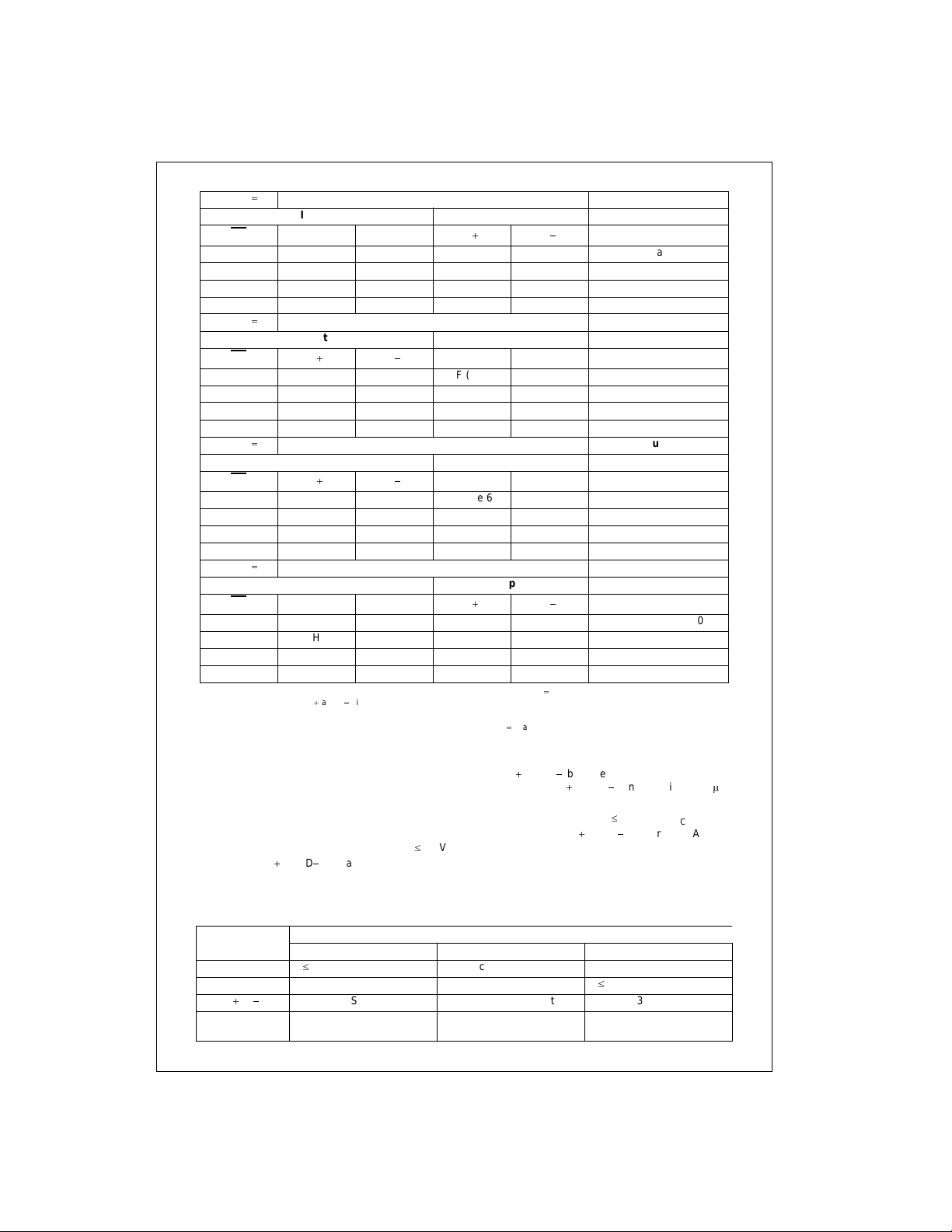
Mode. Table 1 describes the specific pin functionality selection and Table 2 describes the specific Truth Tables for
Driver, Receiver, and Suspended operating functions.
The USB1101 has the capability of serving Self Powered
power supply configu rations only but interfaces to mixed
voltage supply applications.
DAT_VP SE0_VM Function
, D Diff Output SE0_VM Output Receiving
(Internal Low Power Mode)
www.fairchildsemi.com 2
Page 3
Preliminary
TABLE 2. Driver, Receiver, and Suspend Function Select
Suspnd
L Transmit Mode
Inputs Outputs
OE
DAT_VP SEO_VM D
L L L L H Differential Logic 0
L H L H L Differential Logic 1
L L H L L SE0
L H H L L SE0
Suspnd
L Receive Mode
Inputs Outputs
OE
D
D
H L L DIFF (Note 5) H
HHLHL
HLHLL
H H H DIFF (Note 5) L
Suspnd
L Receive Mode While Suspended
Inputs Outputs
OE
D
D
H L L L (Note 6) H
H H L H (Note 6) L
H L H L (Note 6) L
H H H H (Note 6) L
Suspnd
H Transmit Mode
Inputs Outputs
OE
DAT_VP SEO_VM D
L L L L H Differential Logic 0
L H L H L Differential Logic 1
L L H L L SE0
L H H L L SE0
Note 5: DIFF denotes that t he output of the differential receiver is out put via DAT_VP when Sus pnd L. This output sh ould also not be ga te d by the SE0 or
SE1 condition when a s kew betw een D
mation.
Note 6: This is the internal single en ded output that is outp ut on to DAT_VP when Suspnd
and D signals could resu lt in the s hort SE0 or S E1 cond ition s. Plea se ref er to Expe ctatio n Note s for further infor-
D
DAT_VP SEO_VM
DAT_VP SEO_VM
D
H and in receive mode.
USB1101
Power Supply Configurations and Options
The modes of power supply operation include:
1. Self Powered Mode: V
is connected to 3.3V source
CC
(3.0V to 3.6V). This external supply connection provides the 3.3V for the USB pull-up sour ce, the receiv er
input and driver output circuitry.
2. Sharing Mode: V
In this mode the D
is connected and VCC is d 0.8V.
CCIO
and D pins are 3-STATE and the
USB1101 allows external signals up to 3.6V to share
TABLE 3. Power Supply Configuration Options
Pin
V
CC
V
CCIO
, D
D
DAT_VP,
Sharing Self Powered Disable
d
0.8V or Not Connected Connected to 3.3V Source Connected to 3.3V Source
1.65V to 3.6V Source 1.65V to 3.6V Source
3-STATE Function of Mode Set Up 3-STATE
H Function of Mode Set Up (Invalid)
SE0_VM
Power Supply Mode Configuration
the D
leakage from D
V
CCIO
3. Disable Mode: V
In this mode the D
device is in low power state.
A summary of the Supply Configuration is described in
Table 3.
3 www.fairchildsemi.com
and D bus lines. Internally the circuitry limits
and D pins (maximum 10PA) and
such that the device is in low power state.
is d 0.5V and VCC is connected.
CCIO
and D pins are 3-STATE and the
d
0.5V or Not Connected
Page 4
Preliminary
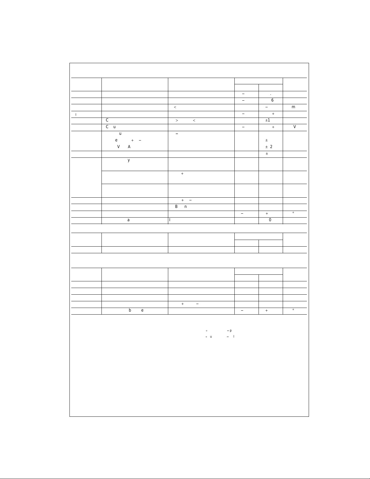
Absolute Maximum Ratings(Note 7)
Symbol Parameter Conditions
USB1101
V
V
I
V
I
V
I
CC
CCIO
IK
I
OK
O
O
Supply Voltage
I/O Supply Voltage
DC Input Current VI 0
DC Input Voltage (Note 8)
DC Output Diode Current VO ! VCC or 0
DC Output Voltage (Note 8)
DC Output Source or Sink VO 0 to V
CC
SE0_VM/DAT_VP
I
, I
CC
GND
V
ESD
DC VCC or GND Current
ESD Immunity Voltage IO, GND, V
CC
HBM (Mil-std. 883E) Pins (Note 8)
MM (ESD_STM 5.2) V
0.5 200 TBD V
CCIO
Pins (Note 9)
CDM (ESD_STM 5.3.1) I
, GND, V
O
CC
Pins (Note 10)
HBM (Mil-std. 883E) Pins D
, D (Note 11) TBD TBD V
USB Connector TBD TBD V
T
STO
P
TOT
Storage Temperature Range
Power Dissipation I
CC
System ESD Testing
System Parameter Conditions
ESDsys IEC61000-4-2 (Note 12) USB Connector TBD TBD V
Limits
Min Max
0.5 4.6 V
0.5 4.6 V
18.0 mA
0.5 V
0.5 V
0.5 V
CCIO
r
18.0 mA
0.5 V
CCIO
r
12.0
r
12.0
r
100 mA
2000 TBD V
1000 2000 V
40.0
125
60.0 mW
Limits
Min Max
Units
mACurrent for D, D Pins
q
C
Units
Recommended Operating Conditions
Symbol Parameter Conditions
V
CC
V
CCIO
V
I
V
AI/O
T
AMB
Note 7: The Absolute Maximum Ratings are those values beyond which the safety of the device cannot be guaranteed. The device should not be operated
at these limits. Th e parametric v alues defined i n the Electric al Characteri stics table are n ot guaranteed at the Absolut e Maximum R atings. The “Re com-
mended Operat ing Conditions” table will define the conditions fo r ac t ual device operation.
Note 8: HBM: Mil-Std_883E compliance. Socketed testing of three units per zap voltage (3
Note 9: MM: ESD_STM 5.2 compliance. Socketed testing of three units per zap voltage (3
Note 10: CDM: ESD_STM 5.3.1 compliance. D ev ices (3 per level) are charged, entire pac k age, and discharged through a single pin contacted to each indi-
vidual pin on the DU T. NC pins are not stres sed . Po sitive and n ega tive c harg e is pl aced on the D UT ( sittin g a top a metallic plate). Maximum stress voltage
applicable at FSM E is 2000V.
Note 11: This test is an extensio n of H BM Mil_Std 883E. However, this test is confined to the differential pins only.
Note 12: IEC61000-4-2 system level testing: System level testing done on this parts evaluation system boar.
DC Supply Voltage 3.0 3.6 V
I/O DC Voltage 1.65 3.6 V
DC Input Voltage Range 0 3.6 V
DC Input Range for AI/O Pins D and D
Operating Ambient Temperature
pulses and 3 pulses). IO v IO, IO v GND, IO v VCC, VCC v GND.
pulses and 3 pulses). IO v IO, IO v GND, IO v VCC, VCC v GND.
www.fairchildsemi.com 4
Limits
Min Max
Units
03.6V
40.0
85.0
q
C
Page 5
Preliminary
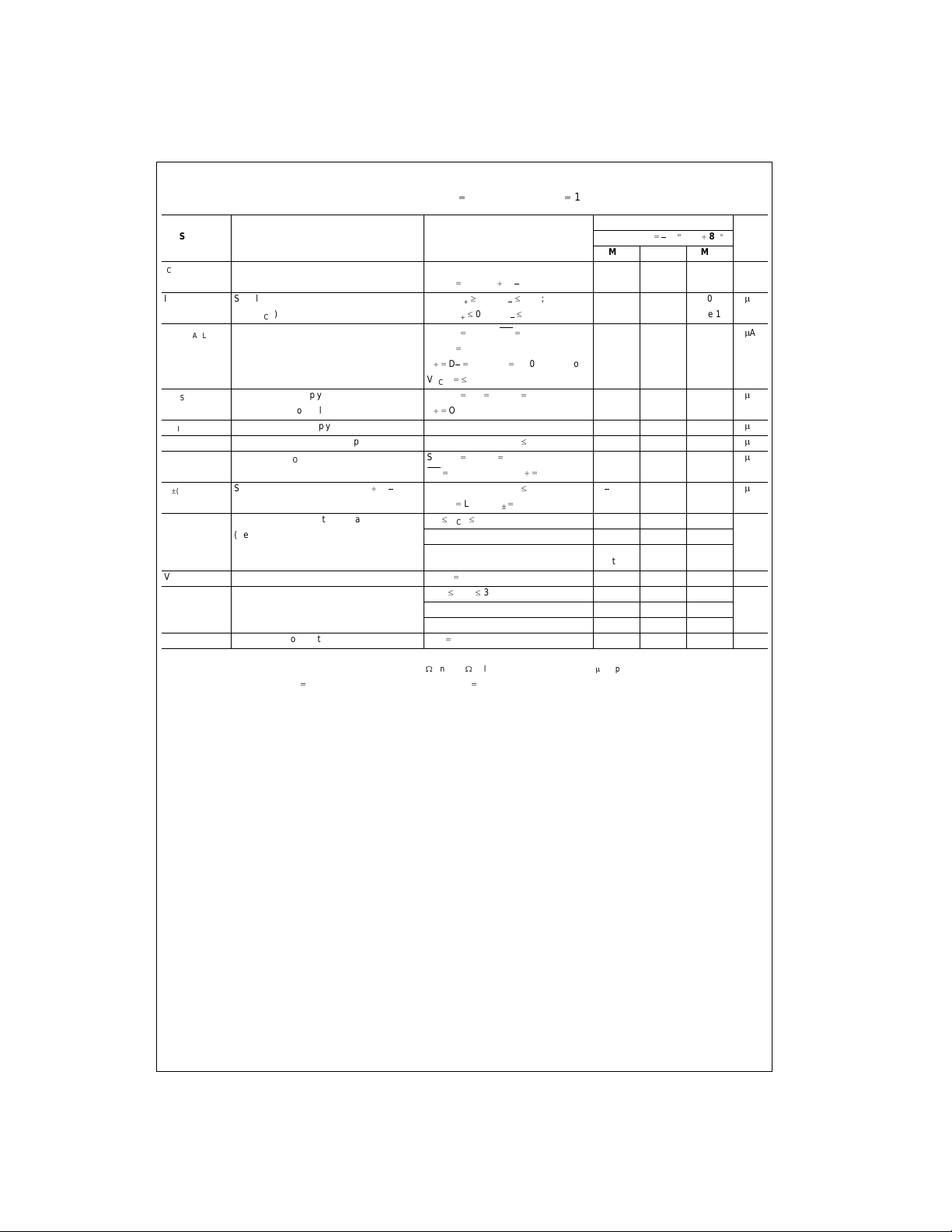
DC Electrical Characteristics (Supply Pins) Over recommended range of supply voltage and
operating free air temperature (unless otherwise noted): V
Symbol Parameter Conditions
I
CC
I
CC(IDLE)
I
CC(DISABLE)
I
CC(SUSPNDR)
I
CCIO(STATIC)
I
CCIO(SHARING)
I
CCIO(SUSPNDR)
I
Dr(SHARING)
V
CCTH
V
CCHYS
V
CCIOTH
V
CCIOHYS
Note 13: Not tested in production, value based on characterization.
Note 14: Excludes any c urrent from load and V
Note 15: Minimum value for V
Operating Supply Current (VCC) Transmitting and receiving at 12Mbit/s; 4.0 8.0 mA
Supply Current During FS IDLE and IDLE: V
SE0 (V
) SE0: V
CC
Disabled Supply Current Suspnd H or L; OE H or L; 20.0
Suspend VCC Supply Current Suspnd OE Config H40.0
(Internal Resistor Pull-up) D Open
I/O Static V
I/O Sharing Mode V
Suspend V
Supply Current IDLE, SE0 20.0
CCIO
CCIO
Supply Current VCC Not Connected or d 0.5V or 0V 20.0PA
CCIO
Supply Current Suspnd Config HIGH; 20.0
Sharing Mode Load Current on D, D Pins VCC Not Connected or d 0.8V
VCC Threshold Detec tion Voltage 3.0 d VCC d 3.6V
(Self Powered) Supply Lost 0.8
VCC Threshold Detection Hysteresis Voltage V
V
Threshold Detection Voltage 3.0V d VCC d 3.6V
CCIO
V
Threshold Detection Hysterias Voltage VCC 3.3V 450 mV
CCIO
current to the 1.5k: and 15k: pull-up/pull-down res is t ors (200 PA typ).
2.0V for supply present condit ion for V
CCTH
SW
3.0V to 3.6V, V
CC
1.65V to 3.6V
CCIO
Limits
Min Typ Max
C
50pF (D, D)
LOAD
t 2.7, V
D
d 0.3V, V
D
d 1.3V; 300
D
d 1.3V (Note 14)
D
Config L
D D DAT_VP SE0_VM = H or L
V
d 0.3V
CCIO
OE HIGH or LOW D Open
Config LOW; V
D
r
3.6V
Supply Present 2.4
1.8V 450 mV
CCIO
10.0 10.0
(Note 15)
Supply Present 1.4
1.8V.
CCIO
USB1101
UnitsTemperature 40qC to 85qC
P
A
P
A
P
A
P
A
P
A
P
A
V
VSupply Lost 0.5
5 www.fairchildsemi.com
Page 6
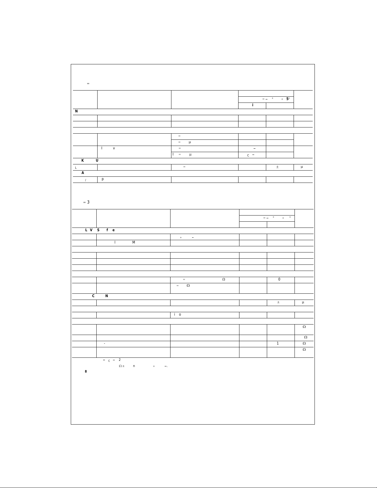
DC Electrical Characteristics (Digital Pins - excludes D, D Pins)
Over recommended range of supply voltage and operating free air temperature (unless otherwise noted).
V
1.65V to 3.6V
CCIO
USB1101
Symbol Parameter Condition
INPUT LEVELS
V
IL
V
IH
OUTPUT LEVELS
V
OL
V
OH
LEAKAGE CURRENT
I
LI
CAPACITANCE
C
, C
IN
LOW Level Input Voltage 0.3 V
HIGH Level Input Voltage 0.6 V
LOW Level Output Voltage IOL 2 mA 0.4
I
100 PA0.15
OL
HIGH Level Output Voltage IOH 2 mA V
IOH 100 PAV
Input Leakage Current V
Input Capacitance Pin to GND 10.0 pF
I/O
1.65V to 3.6V
CCIO
Limits
Min Max
CCIO
0.4
CCIO
0.15
CCIO
DC Electrical Characteristics (Analog I/O Pins - D, D Pins)
Over recommended range of supply voltage and operating free air temperature (unless otherwise noted).
V
3.0V to 3.6V
CC
Symbol Parameter Condition
INPUT LEVELS - Differential Receiver
V
DI
V
CM
Differential Input Sensitivity | V
Differential Common Mode Voltage 0.8 2.5 V
I(D)
- V
|0.2V
I(D)
INPUT LEVELS - Single-ended Receiver
V
IL
V
IH
V
HYS
LOW Level Input Voltage 0.8 V
HIGH Level Input Voltage 2.0 V
Hysteresis Voltage 0.4 0.7 V
Output Levels
V
OL
V
OH
LOW Level Output Voltage Config HIGH for Internal 1.5k: to 3.6V 0.3 V
HIGH Level Output Voltage RL 15K: to GND 2.8
LEAKAGE CURRENT
I
OZ
Input Leakage Current OFF State
CAPACITANCE
C
I/O
I/O Capacitance Pin to GND 20.0 pF
RESISTANCE
Z
DRV
Z
IN
R
PU
R
SW
Note 16: If V
Note 17: Includes external 33
Note 18: See USB2.0 Resistor ECN.
Note 19: Not production tested, guaranteed by de s ign.
Driver Output Impedance Steady State 34.0
Driver Input Impedance 10.0 M
Pull-up Resistance (Note 18) IDLE 900 1575
Switch Resistance 10.0
VCC 0.2V.
OHmin
: r
1% on both pins D and D.
Limits
Min Max
(Note 16)
(Note 17)
Preliminary
UnitTemperature 40qC to 85qC
CCIO
r
1.0
r
1.0
44.0
(Note 19)
P
UnitTemperature 40qC to 85qC
V
V
V
V
A
V
P
A
:
:
:
:
www.fairchildsemi.com 6
Page 7
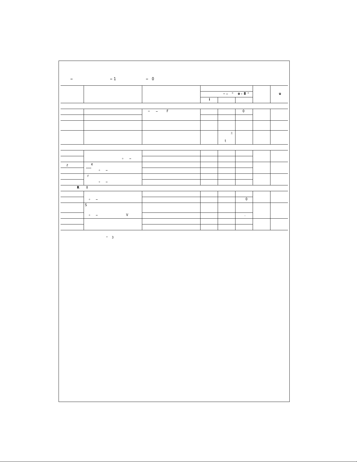
AC Electrical Characteristics (A I/O Pins, Full Speed)
Over recommended range of supply voltage and operating free air temperature (unless otherwise noted).
V
3.0V to 3.6V, V
CC
Symbol Parameter Condition
DRIVER CHARACTERISTICS
t
R
t
F
t
RFM
V
CRS
(Note 20)
Output Rise Time CL 50 125pF 4.0 20.0
Output Fall Time 10% to 90% |VOH - VOL | 4.0 20.0
Rise/Fall Time Match tR / tF Excludes First Transition
Output Signal Crossover Voltage Excludes First Transition from IDLE
DRIVER TIMING
t
PLH
t
PHL
t
PHZ
t
PLZ
t
PZH
t
PZL
Propagation Delay 18.0
(DAT_VP, SE0_VM to D / D) 18.0
Driver Disable Delay 15.0
(OE to D / D) 15.0
Driver Enable Delay 15.0
(OE to D / D) 15.0
RECEIVER TIMING
t
PLH
t
PHL
t
PLH
t
PHL
t
PLH
t
PHL
Note 20: Not production tested, guaranteed by design.
Note 21: Typical conditions (25
Propagation Delay (Diff) 18.0
(D / D to DAT_VP) 18.0
Single Ended Receiver
Propagation Delay
(D / D to DAT_VP, SE0_VM) 18.0
Suspend to DAT_VP 15.0
1.65V to 3.6V, CL 50pF
CCIO
q
C, 3.3V).
from IDLE State
State
Limits
Min Typ Max Number
90.0 111.1 %
1.3 VCC/2 r
200 mV
(Note 21)
2.0 V
18.0
15.0
Preliminary
UnitTemperature 40qC to 85qCFigure
Figures
ns
1, 5
Figures
2, 4
Figures
ns
2, 5
Figures
ns
4, 6
Figures
ns
4, 6
Figures
ns
3, 7
Figures
ns
3, 7
ns
USB1101
7 www.fairchildsemi.com
Page 8
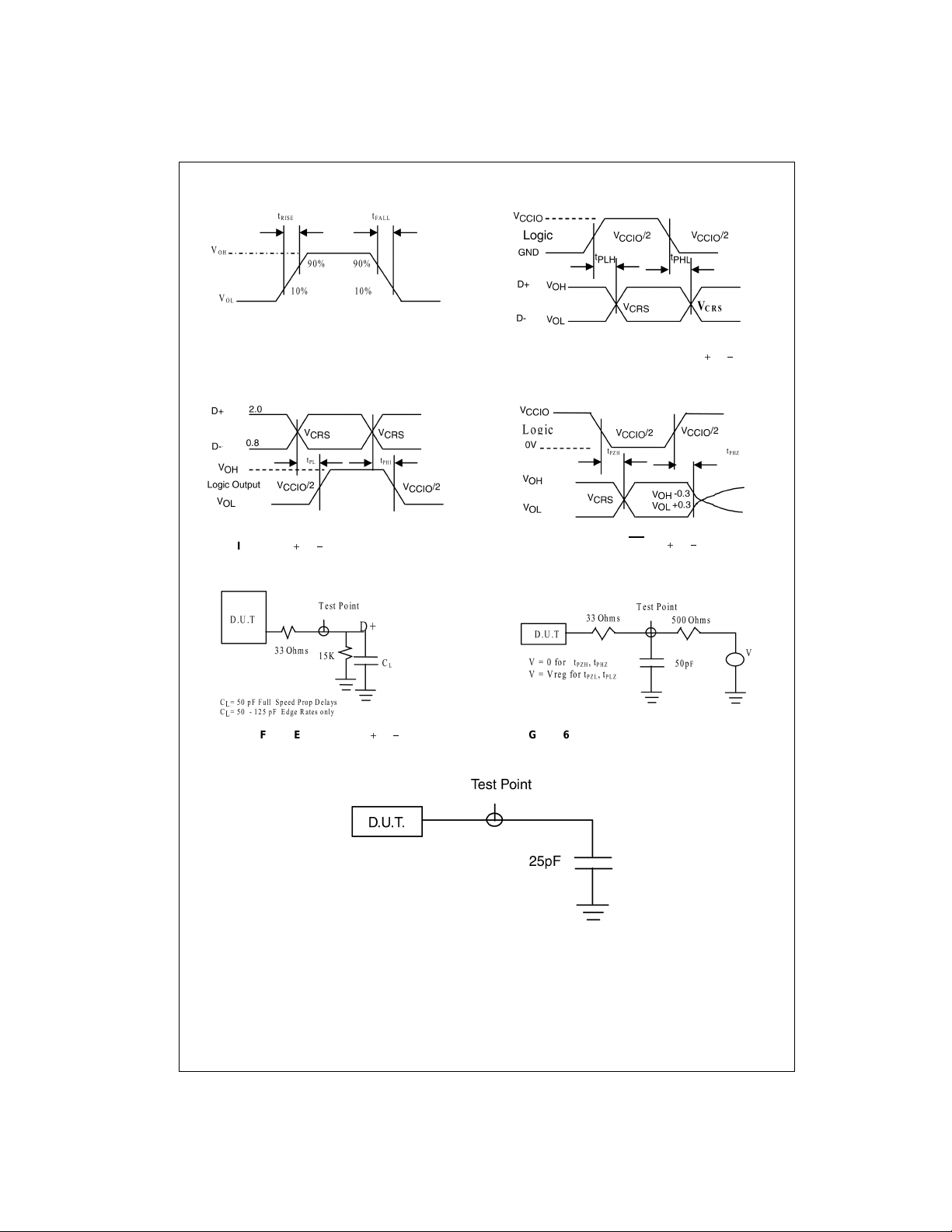
Loading and Waveforms
USB1101
Preliminary
FIGURE 1. Rise and Fall Time
FIGURE 3. D / D to DAT_VP, SE0_VM
FIGURE 5. Load for D / D
FIGURE 2. DAT_VP, SE0_VM to D
FIGURE 4. OE
FIGURE 6. Load for Enable and Disable Time
to D / D
/ D
FIGURE 7. Load for DAT_VP, SE0_VM in Receive Mode
www.fairchildsemi.com 8
Page 9
Preliminary
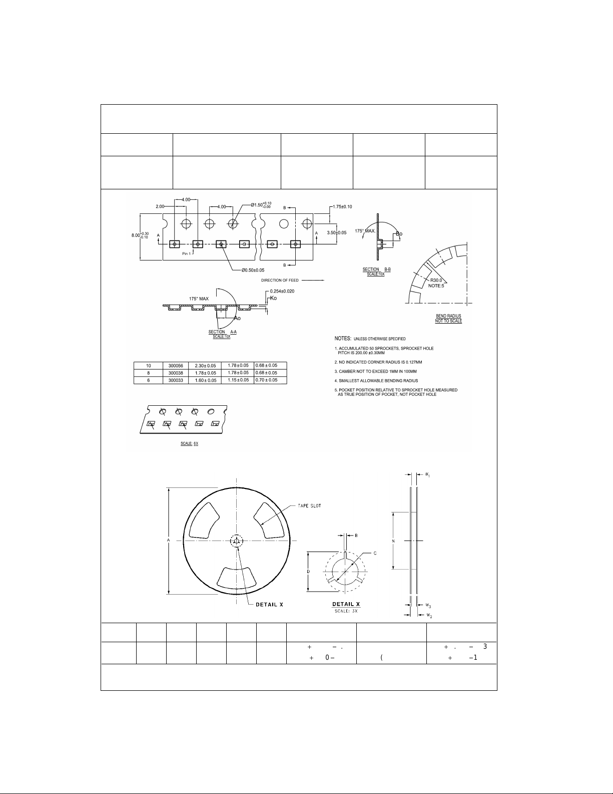
Tape and Reel Specification
Tape Format For Micropak 10
Package Tape Number Cavity Cover Tape
Designator Section Cavities St atus Status
Leader (Start End) 125 (typ) Empty Sealed
L10X Carrier 5000 Filled Sealed
Trailer (Hub End) 75 (typ) Empty Sealed
USB1101
REEL DIMENSIONS inches (millimeters)
Tape
Size
8 mm
ABCDN W1 W2 W3
7.0 0.059 0.512 0.795 2.165 0.331
(177.8) (1.50) (13.00) (20.20) (55.00) (8.40
0.059/0.000 0.567 W1 0.078/0.039
1.50/0.00) (14.40) (W1 2.00/1.00)
9 www.fairchildsemi.com
Page 10
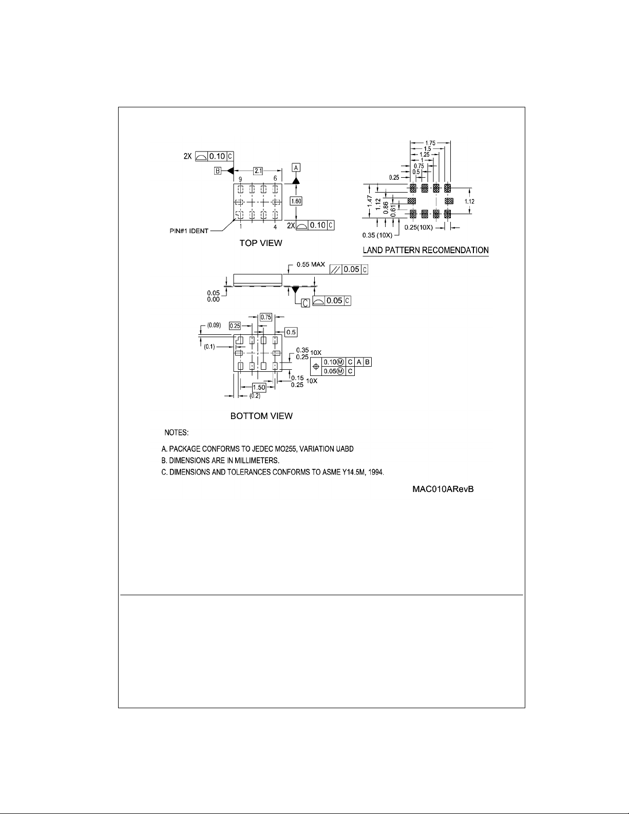
Physical Dimensions inches (millimeters) unless otherwise noted
Preliminary
USB1101 USB 2.0 FS Peripheral Transceiver (Preliminary)
10-Lead MicroPak, 1.6 mm x 2.1mm
Package Number MAC010A
Fairchild does not assume any responsibility for use of an y circuitry described, no circuit patent licenses are imp lied and
Fairchild reserves the right at any time without notice to change said circuitry and specifications.
LIFE SUPPORT POLICY
FAIRCHILD’S PRODUCTS ARE NOT AUTHORIZED FOR USE AS CRITICAL COMPONENTS IN LIFE SUPPORT
DEVICES OR SYSTEMS WITHOUT THE EXPRESS WRITTEN APPROVAL OF THE PRESIDENT OF FAIRCHILD
SEMICONDUCTOR CORPORATION. As used herein:
1. Life support devices or systems a re devices or syste ms
which, (a) are intended for surgical implant into the
body, or (b) support or sustain life, and (c) whose failure
to perform when properly used in accordance with
instructions for use provided in the labeling, can be reasonably expected to result in a significant inju ry to the
user.
2. A critical component in any com ponen t of a life su pport
device or system whose failu re to perform can be reasonably expected to cause the failure of the li fe su pp ort
device or system, or to affect its safety or effectiveness.
www.fairchildsemi.com
www.fairchildsemi.com 10
 Loading...