

Page 1
查询USB100供应商
PRELIMINARY
USB100
Programmable Low-Cost USB Machine (PLUM)
Single Chip Controller for Mouse, Trackball, Joystick and Gamepad Applications
USB100 Programmable Low-Cost USB Machine (PLUM)
January 1999
General Description
The USB100 is a Low cost, fully customizable controller for USB
HID-class pointing devices. It is in full compliance with REV 1.0
of the USB standard and implements the HID class specification
for mice, trackballs, joysticks and gamepads. This device interprets the commands specified in the HID class document and
provides appropriate responses from an On-Chip EEPROM. It
also provides ability to customize the device according to individual needs of the designers. Programming utilities supplied with
this device allow HID manufacturers to easily create the necessary data to be programmed into the device.
The device includes the necessary transceiver for USB operation
and meets all of the active and standby current specifications for
a bus-powered device.
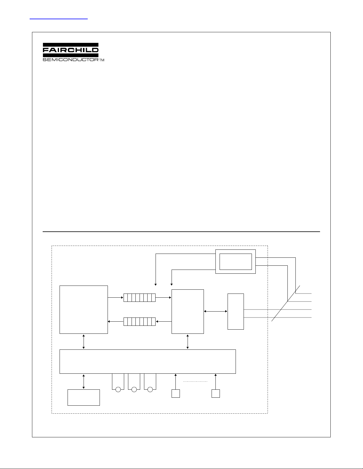
Block Diagram
Features
■ USB 1.0 standard compliant
■ Has the necessary on-chip transceivers
■ Support for 2D and 3D mice with 2, 3 or more buttons
■ Supports 3 potentiometer mechanisms for joysticks
■ Up to 16 buttons for digital gamepads
■ Choice of 18-pin and 24-pin packages
■ Choice of 2Kbit and 4Kbit EEPROM densities
POWER
USB
COMMAND
PROCESSOR
(HID)
EEPROM
USB100 rev.D
© 1999 Fairchild Semiconductor Corporation
TX-FIFO
RX-FIFO
STATE MACHINE
UP TO 3 ROLLER/
POTENTIOMETER
MECHANISMS
SERIAL
INTERFACE
ENGINE
UP TO 16 BUTTONS
1
X
C
V
R
Use "A Diagram Number" Style Sheet"
USB CABLE
(D+, D-,
POWER &
GROUND)
www.fairchildsemi.com
Page 2
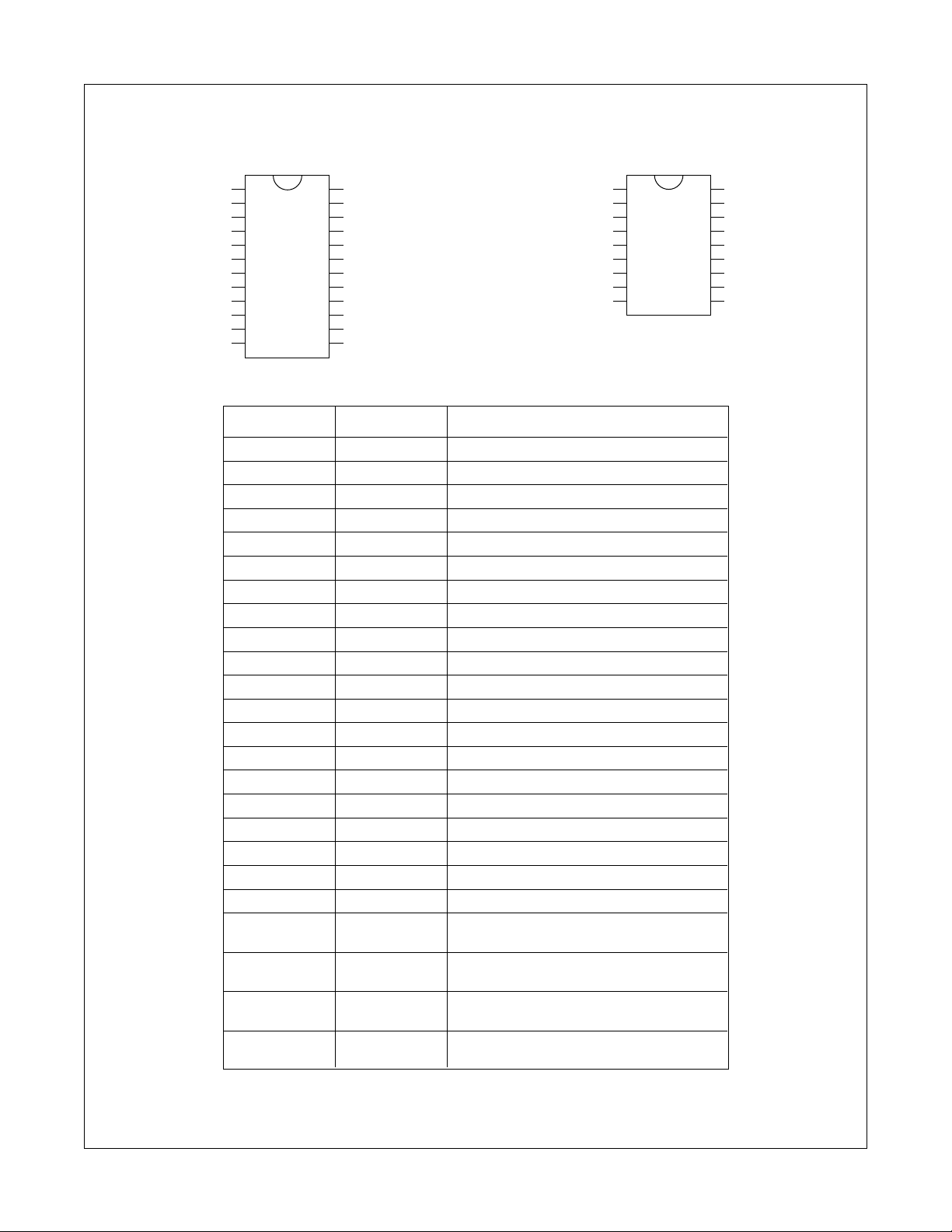
Pinout
USB100 Programmable Low-Cost USB Machine (PLUM)
24 Pin Package 18 Pin 3D Package
OSC1 VDD
OSC2 B6
H4 USBD+
B8/F USBD-
RESET GND
H3 B7
H1 B5
H2 B1
V1 B2
V2 B3
O2 B4
GND O1
Pin Description
Pin Type Description
H4 I Roller/Button/Joystick input.
H3 I Roller/Button/Joystick input.
O2 I/O Register output pin / Button input.
OSC1 I Crystal input number 1.
OSC2 I Crystal input number 2
B4 I Button input
Reset I Active high reset pin
H1 I Roller/Button/Joystick input.
H2 I Roller/Button/Joystick input.
V1 I Roller/Button/Joystick input.
V2 I Roller/Button/Joystick input.
GND I Ground
B7 I Button input
B6 I Button input
B5 I Button input
VDD I Positive power supply
USBD+ O USB D + line
USBD- O USB D – line
GND I Ground
B8/F I/O Button input / LED driver
B1/CS I Button input and chip select to internal
B2/SK I Button input and system clock to internal
B3/DI I Button input and data in to internal
O1/DO O Button input and data out to read from
* See Programming internal EEPROM section
OSC2 OSC1
H4 VDD
F USBD+
RESET USBD-
H3 GND
H1 B1
H2 B2
V1 B3
V2 O1
EEPROM.*
EEPROM.*
EEPROM.*
internal EEPROM.*
USB100 rev.D
2
www.fairchildsemi.com
Page 3

USB100 Programmable Low-Cost USB Machine (PLUM)
Absolute Maximum Ratings
Ambient Storage Temperatures -65°C to + 150°C
All Input or Output Voltages with VCC + 1 to – 0.3V
Operating Conditions
Ambient Operating Temperature 0°C to +70°C
Power Supply (VCC) Range 4.4V to 5.5V
respect to ground
Lead Temperature +300%
(Soldering, 10 seconds)
ESD Rating 2000V
DC and AC Electrical Characteristics 4.4V ≤ VCC ≤ 5.5V
Symbol Parameter Conditions Min Max Units
I
CCA
I
CCS
V
IL
V
IH
V
OL
V
OH
I
IL
I
OL
F
SK
T
SKH
T
SKL
T
CS
T
CSS
T
DH
T
DIS
T
CSH
T
DIH
T
PD1
T
PD0
T
SY
T
DF
T
WP
Operating Current USB interface in active mode 40 mA
Standby Current USB interface in suspend 500 µA
Input Low Voltage 0.8 V
Input High Voltage 2 V
Output Low Voltage 0.4 V
Output High Voltage 2.4 V
Input Leakage Current 2.5 µA
Output Leakage Current 2.5 µA
SK Clock Frequency Note 3 0 1 MHz
SK High Time 250 ns
SK Low Time 250 ns
Minimum CS Low Time Note 4 250 ns
CS Setup Time 50 ns
DO Hold Time 70 ns
DI Setup Time 100 ns
CS Hold Time 0 ns
DI Hold Time 20 ns
Output Delay to “1” 500 ns
Output Delay to “0” 500 ns
CS to Status Valid 500 ns
CS to DO in TRI-STATE 100 ns
Write Cycle Time 10 ms
AC Test Conditions
Output Load 1 TTL Gate
Input Pulse Levels 0.4V and 2.4V
Note 1: Stress ratings above those listed under “Absolute Maximum Ratings” may cause permanent damage to the device. This is a stress rating only and operation of the
device at these or any other conditions above those indicated in the operational sections of the specification is not implied. Exposure to absolute maximum rating conditions for
extended periods may affect device reliability.
Note 2: The shortest allowable S clock period = 1/fSK (as shown under the fSK parameter). Maximum SK clock speed (minimum SK period) is determined by the interaction of
several AC parameters stated in the datasheet. Within this SK period, both t
t
(minimum) for shorter SK cycle time operation.
SKL
Note 3: CS (Chip Select) must be brought low (to VIL) for an interval of tCS in order to reset all internal device registers (device reset) prior to beginning another opcode cycle.
(This is shown in the opcode diagrams in the following pages.)
USB100 rev.D
SKH
and t
Timing Measurements Reference Level
Input 1V and 2V
Output 0.8V and 2.0V
limits must be observed. Therefore, it is not allowable to set 1/fSK = t
SKL
3
SKH
www.fairchildsemi.com
(minimum) +
Page 4
USB100 Programmable Low-Cost USB Machine (PLUM)
USB100
F
VDD
Interface Pin Descriptions
H1, H2, H3, H4, V1, V2 (Roller/Joystick inputs)
When configured as roller inputs these pins function in pairs, H1
and H2, H3 and H4, V1 and V2 to allow photo diodes to be
attached in a mouse or trackball application. See the section
“Roller Movement Reporting” for a more detailed description.
When configured for a joystick only one of the inputs pairs is used.
A potentiometer is attached to track the movements of a joystick
lever. When these inputs are configured as buttons they all act
independently as active low button inputs. All of them have
internal pull-ups and debounce circuitry which can be programmed
using the ICB registers. These inputs also contain current sink
features so no external resistor is needed to sink current from the
photo diode.
B1, B2, B3, B4, B5, B6, B7, B8/F (Button inputs)
The button inputs to the USB100 have internal pull up resistors,
with active low inputs to the chip. These inputs also contain
debounce circuitry which can be programmed by the ICB registers.
Key Debounce Select Table (ICB register3[3:2])
KD[1:0]
00 15 ms
01 30 ms
10 45 ms
11 60 ms
O1, O2 Functionality. ICB register 1[3:2]
IOM[1:0] Function
00 Both O1 and O2 function as programmable
outputs.
01 O1 is a programmable output but O2 is a
standard button input.
11 Both O1 and O2 are standard inputs.
In case these are selected as outputs, their state (1 or 0) can be
set using the USB set_report command. These outputs are opencollector. A typical use of these outputs is using them to drive LEDs
(for example, a drag-lock function in a trackball). These pins have
a programmable current sink capability.
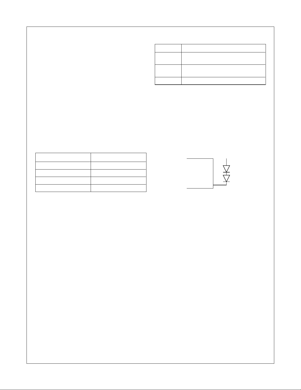
B8/F
When this pin is configured as an input it will behave as a standard
button input. But if the pin is disabled in the ICB registers then this
pin can be used to control the roller LEDS in powersave mode.
Using the B8/F pin to control the LEDs
USBD -, USBD +
These inputs are the serial bus lines which USB data is communicated. These bi – directional lines connect to the host, through
a USB type A or type B connector, and are used to communicate
all USB information to and from the host. The two lines must both
be wired through a 27 ohm resistor before being attached to the
USB connector. See Recommended Configuration for a detailed
diagram.
Reset
This pin is used to reset the entire chip. It must be held high for
more than 10ns, to reset the chip and then brought low for the reset
of normal chip operation.
O1, O2
These two pins are wired to internal registers which can be
programmed with either a “1” or a “0” by a USB request. If this
command is sent to the USB100. INSERT COMMAND FROM
INSPECTOR. Then the O1 and O2 pins will be programmed with
the values that are in the second data package. These two pins
can also be configured as standard button inputs by one of the ICB
registers.
This allows the LEDs to be shut off during powersave mode which
allows the USB100 to draw very little current. The official name for
powersave mode on a USB device is known as suspend mode
which is discussed in the section labeled Suspend Mode Operation.
OSC1, OSC2
These two pins are the clock inputs into the USB100. The speed
at which the chip runs at is 6MHz. The clock sign can be generated
two ways. The first is to use a parallel resonant, fundamental mode
crystal circuit or a ceramic resonator circuit connected to the
OSC1 and OSC2 inputs. The other method is to use a crystal
oscillator connected to the OSC2 input and leaving the OSC1
input unconnected
USB modes of operation
The USB100 loads up its configuration from the EEPROM on
power-on reset, or when a USB reset command is issued. Upon
completion of reset, the device is in a operational mode, and
responds correctly to the various commands described in the USB
spec rev 1.0. The USB100 supports two endpoints – the default
endpoint (endpoint 0) and the interrupt endpoint (endpoint 1). The
supported packet size on both endpoints is 8 bytes. The endpoint
1 is an “IN” endpoint.
USB100 rev.D
4
www.fairchildsemi.com
Page 5
USB100 Programmable Low-Cost USB Machine (PLUM)
Standard Requests
The USB100 supports all of the required standard requests.
These requests are sent to the device using control transfers to
endpoint 0.
In USB terminology, the data transmitted by the mouse when
movement is detected is called a report. The reports are generated by the USB100 device in accordance to the USB HID spec
1.0 Final.
Programming the EEPROM
The on-chip EEPROM can be programmed in a special mode
which defines some of the button inputs/output as a microwire
port.. In this mode, these inputs behave as a conventional Microwire
serial port. Data can be easily programmed and verified, by
executing simple EEPROM programming commands.
Initial Configuration Bytes (ICB) register
description
The first five bytes in the EEPROM are used to configure the
physical characteristics of the USB100 device, and are called the
Initial configuration Byte registers. Some of the bits in these
registers are reserved, and are referred to as RFU (reserved for
future use) in the following section.
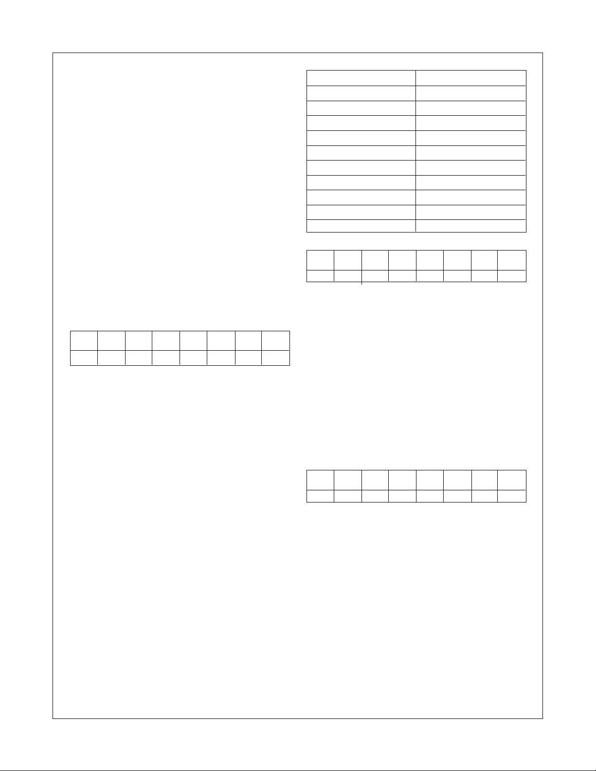
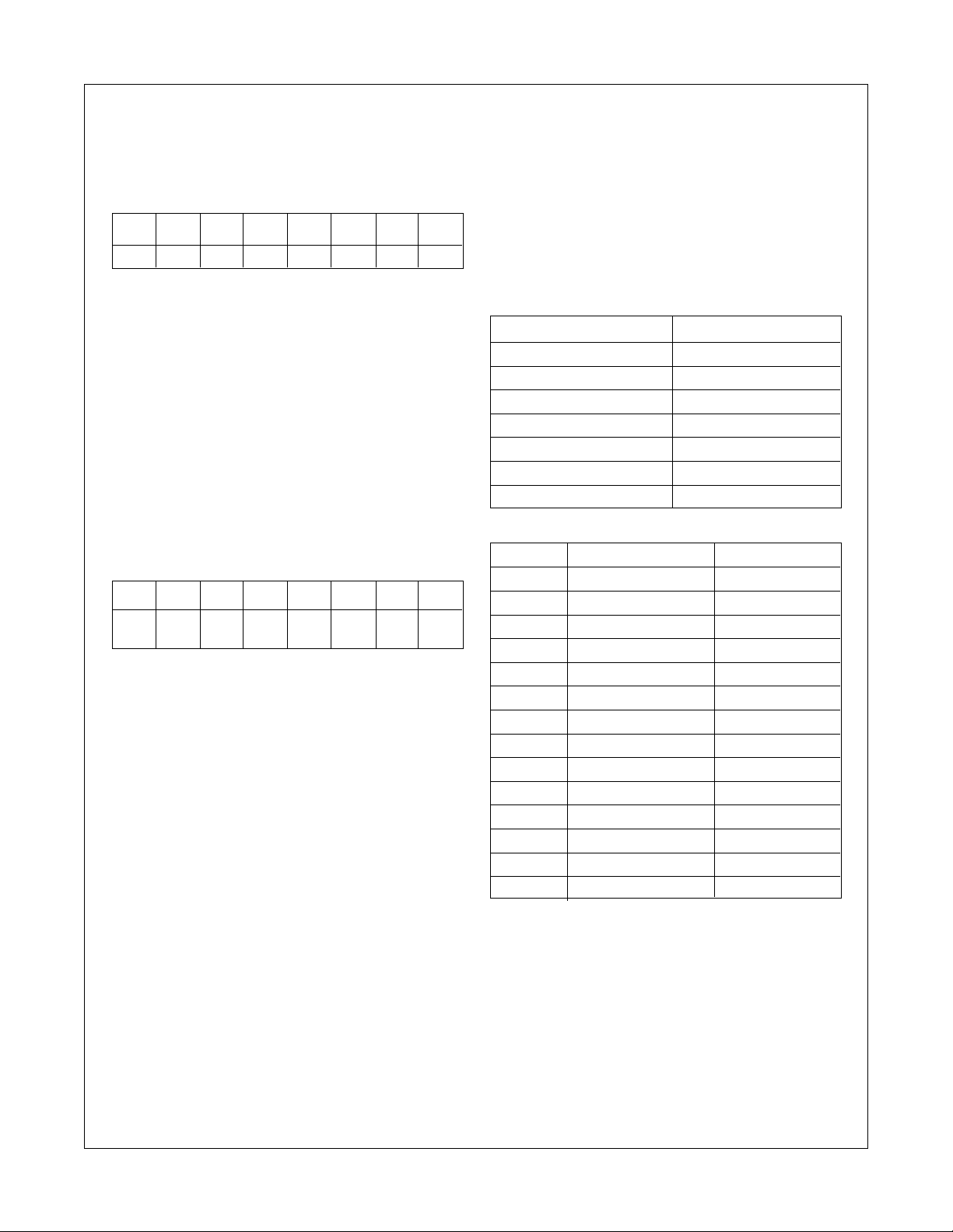
Roller Configuration Byte (Address 0)
D7 D6 D5 D4 D3 D2 D1 D0
IS3 IS2 IS1 IS0 IOM1 IOM0 R1 R0
R[1:0]: No of roller pairs. This pair of bits configure the functionality of the three roller pair inputs – <H1, H2>, <V1,V2> and <H3,
H4>.
00: No rollers on this device, all roller inputs are available as
general purpose inputs
01: H1, H2 are the only roller mechanism active. The other
roller inputs are available as general purpose inputs.
10: H1, H2 and V1 and V2 are defined as roller mechanism
pairs. The other pair is still available as general purpose
inputs.
11: All the three pairs of roller inputs function as roller inputs.
It must be noted that the reassignment of the rollers must be done
only as follows: If the application needs to use only one roller – use
H1 and H2. Two rollers – use H1, H2 and V1, V2, Three rollers –
use H1, H2, V1, V2 and H3, H4. Any other choice for roller use is
illegal and results in unpredictable device behavior.
IOM[1:0]: I/O functionality of the O0 and O1 pins. When IOM0 is
set to ‘0’, the O0 bit functions as an output. When set to ‘1’ it
becomes an input. . When IOM1 is set to ‘0’, the O1 bit functions
as an output. When set to ‘1’ it becomes an input. The only valid
combinations for these bits are 00, 01 and 11 respectively.
IS[3:0]: This 4-bit value is to set the amount of current that an
external device can sink into the H1, H2, V1, V2 and H3 and H4
inputs When these bits are set to 0000 the current sink is set to 0.1
mA on each of the inputs. In can be varied in steps of 0.1mA up
to a max of 1 mA.
IS[3:0] Current
0000 0.1 mA
0001 0.2 mA
0010 0.3 mA
0011 0.4 mA
0100 0.5 mA
0101 0.6 mA
0110 0.7 mA
0111 0.8 mA
1000 0.9mA
1001 1.0mA
Input Pin Configuration Byte 0 (ICB0) (Address 1)
D7 D6 D5 D4 D3 D2 D1 D0
B8 B7 B6 B5 B4 B3 B2 B1
B[7:0]: Input Pin Report Generator. A ‘1’ causes this bit to be
reported in the corresponding report generated when the device
is polled for the status. The device accepts only the following bit
patterns as valid. B[7:0] control the functionality for pin inputs
B[8:1] respectively.
00000000
00000001
00000011
00000111
00001111
00011111
00111111
01111111
11111111
Input Pin Configuration Byte 1 (ICB1) (Address 2)
D7 D6 D5 D4 D3 D2 D1 D0
IO1 IO0 EB5 EB4 EB3 EB2 EB1 EB0
EB[5:0]: Input Pin Report Generator, Extended byte. The functionality of this register is influenced by the roller configuration
byte. A ‘1’ causes this bit to be reported in the corresponding report
generated when the device is polled for the status. EB0 corresponds to H3 and EB1 corresponds to H4. EB2 corresponds to V1
and EB3 corresponds to V2. EB4 corresponds to H1 and EB5
corresponds to H2.
00000000
00000001
00000011
00000111
00001111
00011111
00111111
USB100 rev.D
5
www.fairchildsemi.com
Page 6
USB100 Programmable Low-Cost USB Machine (PLUM)
RFU: Reserved for future use, must be set to 0.
IO[1:0]: When the IO pins are reconfigured as inputs, a ‘1’ in the
corresponding bit position will cause the input to be included in the
report generator.
Application Configuration Byte (Address 3)
D7 D6 D5 D4 D3 D2 D1 D0
FIS3 FIS2 FIS1 FIS0 KD1 KD0 F1 F0
F[1:0]: Function Select. Selects between the following
00 : Mouse operation
01: RFU
10: Joystick Operation.
11: Digital Gamepad operation
KD[1:0]: Key Debounce Select:
00: 15 Ms
01: 30 Ms
10: 45 Ms
11: 60 Ms
FIS[3:0]: These bits select the amount of current that the ‘F’ pin
can sink, in 1 mA increments. When FIS[3:0] = “0000” The current
sink is set at 2 mA. Incrementing this count by 1 will cause the
current to be increased by 1mA The maximum value is 10 mA.
Remote Resume Config Byte (Address 4)
D7 D6 D5 D4 D3 D2 D1 D0
RFU RFU RFU RFU RRES RRES RRES RRES
_EN 2 1 0
RRES_EN: Remote_resume enable. This bit, when set, enables
remote resume operation.
RRES[2:0]: Duration Select. When the device has entered in
suspend mode, these bits select the duration after which an
internal “momentary wakeup” is done to check whether there has
been any movement on the rollers in the mouse mode or the
potentiometers in the joystick mode. The RRES_EN bit must be
set to 1 to enable this feature.
000: 15 ms
001: 30 ms
010: 45 ms
011: 60 ms
100: 75 ms
101: 90 ms
110: 105 ms
111: Reserved for future use (do not use this combination,
unpredictable operation could result)
Descriptor Setup
The EEPROM stores a Descriptor Description Table (DDT) followed by the actual descriptors (DES). The DDT begins at byte
address 8 in the EEPROM. It consists of 14 Words. Each Word
consists of two bytes – The first byte is a byte indicating the type
of descriptor (these byte values are indicated in the USB specification). The second byte is an address. This address indicates the
first byte of this descriptor in the EEPROM. An unimplemented
descriptor table entry begins with a 00. The following table shows
a possible configuration.
Address Map
Memory AddressRange Data type
08-35 Descriptor Description Table
36-53 Device Descriptor
54-62 Config Descriptor
63-71 Interface Descriptor
72-78 Mouse HID Class Descriptor
79-86 Endpoint Descriptor
87-118 String Descriptor
Descriptor Description Table (for above example)
Address Descriptor type Memory Offset
08 Device 36
10 Config 54
12 Interface 63
14 Mouse-HID 72
16 Endpoint 78
18 String 87
20 00 00
22 00 00
24 00 00
26 00 00
28 00 00
30 00 00
32 00 00
34 00 00
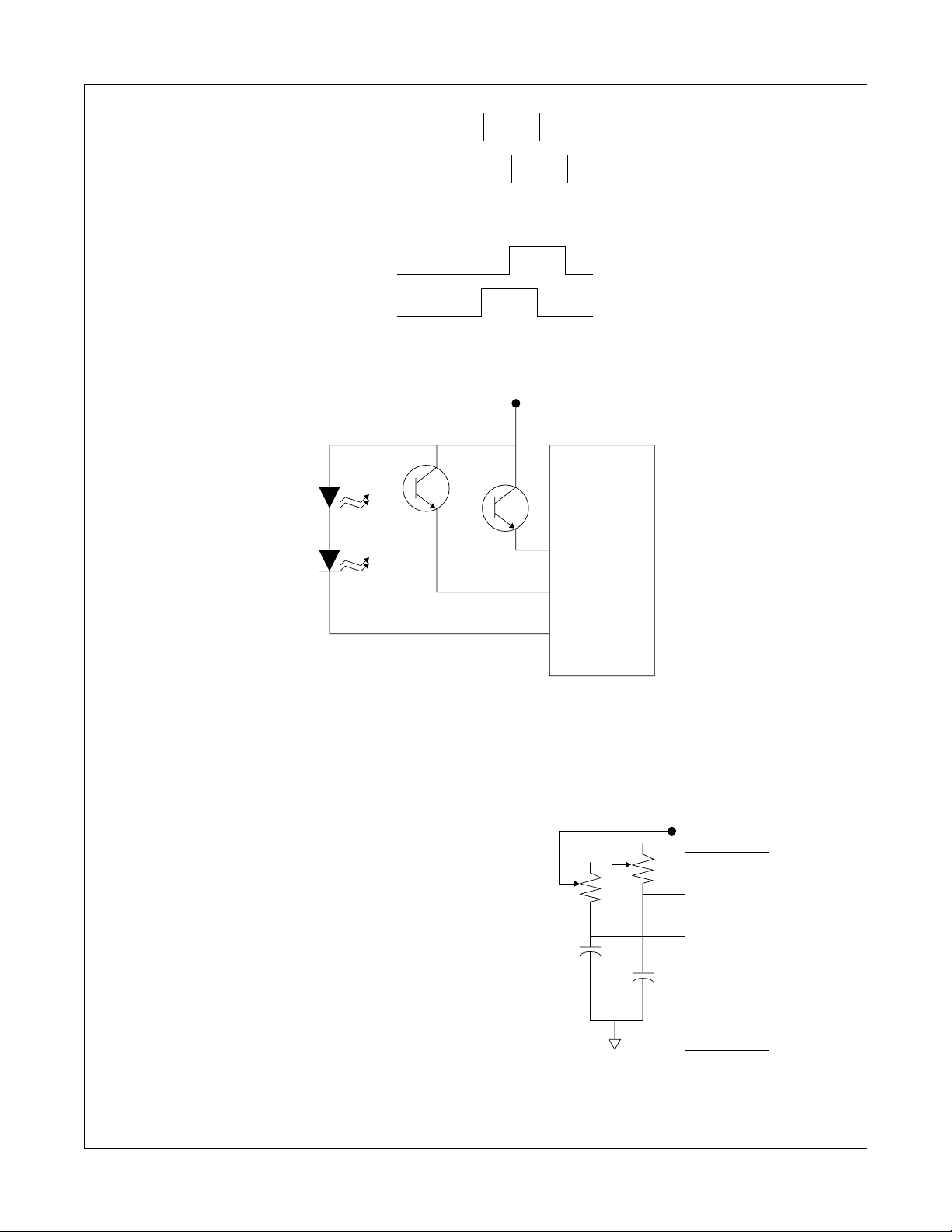
Roller Movement Reporting
The roller mechanism built on the USB100 is capable of interfacing either to a LED-chopper wheel-Phototransistor system or a
mechanical system using a commutator with wiper contacts.
USB100 rev.D
6
www.fairchildsemi.com
Page 7
H1 or V1 or H3
H2 or V2 or H4
Negative Counting
H1 or V1 or H3
H2 or V2 or H4
Positive Counting
USB100 Programmable Low-Cost USB Machine (PLUM)
v
D1
D2
Schematic 1: Roller Mode of Operation
When the Roller configuration register is used to define an input
pair as roller inputs, the corresponding roller movement reporting
is enabled. In this case, internally, the roller wheel pulses are
counted and registered into an 8 bit register. One register is
available per input pair. A total of three rollers movement registers
(RMRs) are available, corresponding to the three roller mechanisms available. On all the input pairs (H1, H2 or V1, V2 or H3, H4)
the positive counting sequence is defined as (0,0), (0,1), (1,1) and
(0,0) and the same sequence repeating over again. Negative
counting sequence is defined as (0,0), (1,0), (1,1) and (0,1) and
the same sequence repeating again. Each of the above transitions
will result in the counter incrementing or decrementing by one
depending on whether the rollers are moving in the positive or
negative direction. Each time an IN query is sent on endpoint 1, the
counter contents are transferred to a temporary holding register
and queued for transmission on the USB. When an ACK is
received for the current transaction, the counter is cleared.
Q1
Q2
USB100
H1
H2
F
Hardware Features
Roller / Potentiometer Interface
One of the key differences between the mouse and joystick
hardware implementation is that themouse uses optical encoding
v
P1
P2
USB100
H1
V1
USB100 rev.D
Schematic 2 : Potentiometer Mode of
Operation for Joystick
7
www.fairchildsemi.com
Page 8
USB100 Programmable Low-Cost USB Machine (PLUM)
and a roller wheel to detect mouse movement. In contrast, joystick
uses a potentiometer to detect angular motion. The function select
bits [F1:0] allow the designer
to set the bits. In a mouse mode, the H1, H2, V1,V2 and H3 & H4
inputs are selected for the roller mechanism decode.In the joystick
mode, it selects the potentiometer interface. The state machine
uses a different algorithm for interpreting the inputs to the chip.
This function selection also affects the format of the report that is
generated.The roller mode is shown in schematic 1 and the
potentiometer mode is shown in schematic 2.
In case of the roller mode of operation (mouse/trackball), the
transitions on the Hx and Vx pairs are used in the counting process
to generate a digital estimate of the motion of the ball. In the
joystick mode of operation, the RC timing constant changes the
width of an internal digital pulse whose width is measured and
reported back. All of the buttons feature an internal pullup. The
actual switches used is a push button switch with one terminal
connected to a button input and the second terminal connected to
ground.
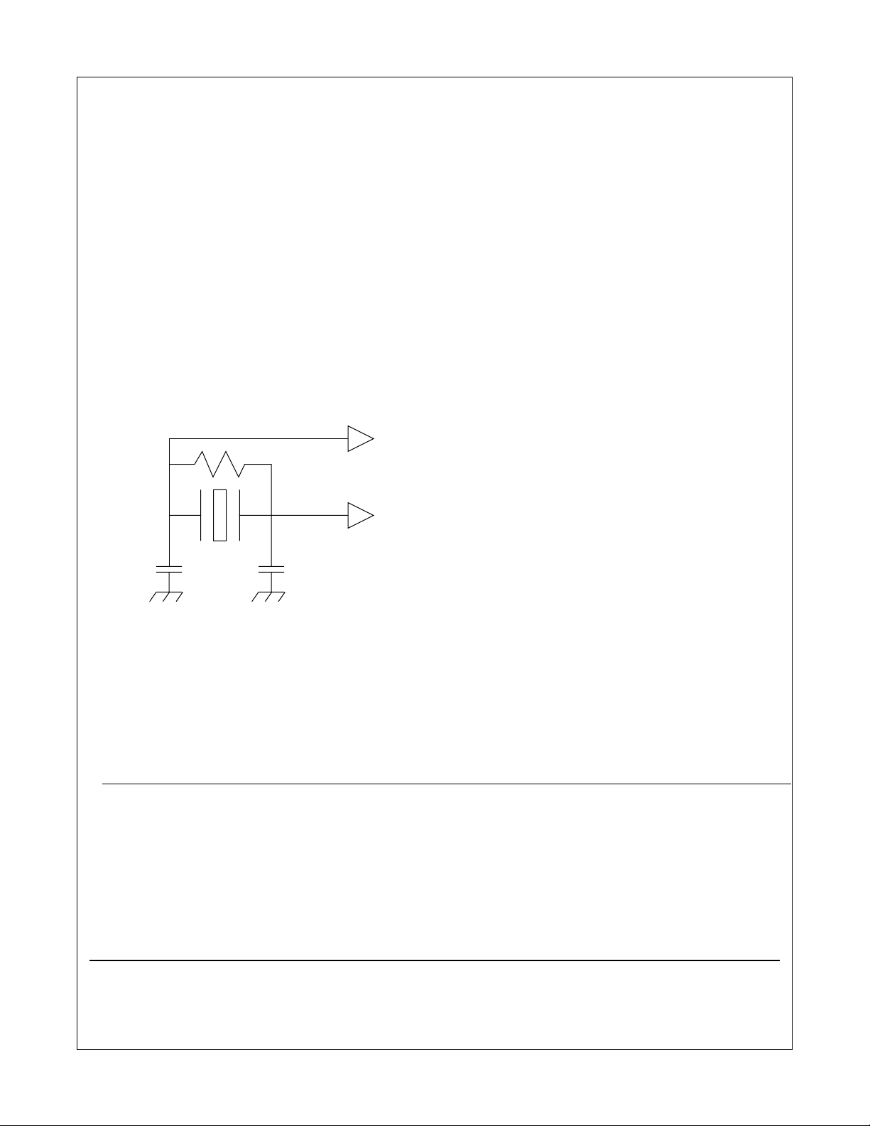
Crystal / Crystal Oscillator combination
OSC1
OSC2
Suspend mode operation
When the PLUM device determines that the necessary conditions
(laid down in the USB standard), it goes into the suspend mode.
It wakes up on USB bus activity, or when any of the buttons are
depressed. There exists an internal timer, whose timing operation
could be selected via bits 3 through 0 in ICB register 5. The PLUM
device wakes up on the expiration of the timer. It senses the roller/
potentiometer interface to determine if these inputs have changed
since the last poll. It does a remote wakeup, when such a
movement has occurred.
Remote Wakeup Support
This device supports the remote wakeup feature. This is indicated
to the host via the corresponding descriptor. Internally, the state
machine uses the values of the RRES_EN and RRES[2:0] bits in
the Remote Resume configuration byte to enable this feature, and
the amount of time between the “polls” to the roller/potentiometer
ports to determine whether the necessary conditions for wakeup
have been met.
The above configuration is the recommended configuration for
use with a crystal or a ceramic resonator. The capacitors are
optional and if used, must be in the 10-30pf range. The resistor is
necessary and its value is 1MΩ. A metal-can oscillator may be
used too. In this case, the output of the oscillator must be
connected to OSC1 and OSC2 must be left unconnected.
Life Support Policy
Fairchild's products are not authorized for use as critical components in life support devices or systems without the express written
approval of the President of Fairchild Semiconductor Corporation. As used herein:
1. Life support devices or systems are devices or systems which,
(a) are intended for surgical implant into the body, or (b) support
or sustain life, and whose failure to perform, when properly
used in accordance with instructions for use provided in the
labeling, can be reasonably expected to result in a significant
injury to the user.
Fairchild Semiconductor Fairchild Semiconductor Fairchild Semiconductor Fairchild Semiconductor
Americas Europe Hong Kong Japan Ltd.
Customer Response Center Fax: +44 (0) 1793-856858 8/F, Room 808, Empire Centre 4F, Natsume Bldg.
Tel. 1-888-522-5372 Deutsch Tel: +49 (0) 8141-6102-0 68 Mody Road, Tsimshatsui East 2-18-6, Yushima, Bunkyo-ku
English Tel: +44 (0) 1793-856856 Kowloon. Hong Kong Tokyo, 113-0034 Japan
Français Tel: +33 (0) 1-6930-3696 Tel; +852-2722-8338 Tel: 81-3-3818-8840
Italiano Tel: +39 (0) 2-249111-1 Fax: +852-2722-8383 Fax: 81-3-3818-8841
2. A critical component is any component of a life support device
or system whose failure to perform can be reasonably expected to cause the failure of the life support device or system,
or to affect its safety or effectiveness.
Fairchild does not assume any responsibility for use of any circuitry described, no circuit patent licenses are implied and Fairchild reserves the right at any time without notice to change said circuitry and specifications.
USB100 rev.D
8
www.fairchildsemi.com
 Loading...