

Page 1
查询USB1T11A供应商
USB1T11A
Universal Serial Bus Transceiver
USB1T11A Universal Serial Bus Transceiver
November 1999
Revised March 2005
General Description
The USB1T11A is a one chip generic USB transceiver. It is
designed to allow 5.0V o r 3.3V programmable and standard logic to interfac e with the physical layer of the Universal Serial Bus. It is capable of transmitting an d receiving
serial data at both full speed (12Mbit/s) and low speed
(1.5Mbit/s) data rates.
The input and output signals of the USB1T11A conform
with the “Seria l Interface Engine”. Implementati on of the
Serial Interface Engine along with the USB1T11A allows
the designer to make US B com pati ble de vices w ith off-th eshelf logic and easily modify and update the application.
Features
■ Complies with Universal Serial Bus specification 1.1
■ Utilizes digital inputs and outputs to transmit and receive
USB cable data
■ Supports 12Mbit/s “Full Speed” and 1.5Mbit/s
“Low Speed” serial data transmission
■ Compatible with the VHDL “Serial Interface Engine”
from USB Implementers' Forum
■ Supports single-ended data interface
■ Single 3. 3V supply
■ ESD Performance: Human Body Model
!
9.5 kV on D, D pins only
!
4 kV on all other pins
■ 16-lead Pb-Free MLP package saves space
Ordering Code:
Order Number
USB1T11AM
(Note 1)
USB1T11AM_NL
(Note 2)
USB1T11ABQX MLP16C Pb-Free 16-Terminal Molded Leadless Package (MLP), JEDEC MO-220, 3mm square
USB1T11AMTC
(Note 1)
USB1T11AMTC_NL
(Note 2)
USB1T11AMTCX_NL
(Note 2)
Pb-Free package per JEDEC J-STD-020B.
Note 1: Device also available in Tape and Reel. Specify by appending suffix letter “X” to the ordering code.
Note 2: “_NL” indicates Pb-Fre e pac k age (per JEDEC J-ST D-020B). Please us e order number as indi c at ed.
Package
Number
M14A 14-Lead Small Outline Integrated Circuit (SOIC), JEDEC MS-012, 0.150" Narrow
M14A Pb-Free 14-Lead Small Outline Integrated Circuit (SOIC), JEDEC MS-012, 0.150" Narrow
MTC14 14-Lead Thin Shrink Small Outline Package (TSSOP), JEDEC MO-153, 4.4mm Wide
MTC14 Pb-Free 14-Lead Thin Shrink Small Outline Package (TSSOP), JEDEC MO-153, 4.4mm
Wide
MTC14 Pb-Free 14-Lead Thin Shrink Small Outline Package (TSSOP), JEDEC MO-153, 4.4mm
Wide
Package Description
The USB-IF Logos ar e trademarks of Unive rs al Serial Bus Implem enters Forum, Inc.
© 2005 Fairchild Semiconductor Corporation DS500234 www.fairchildsemi.com
Page 2
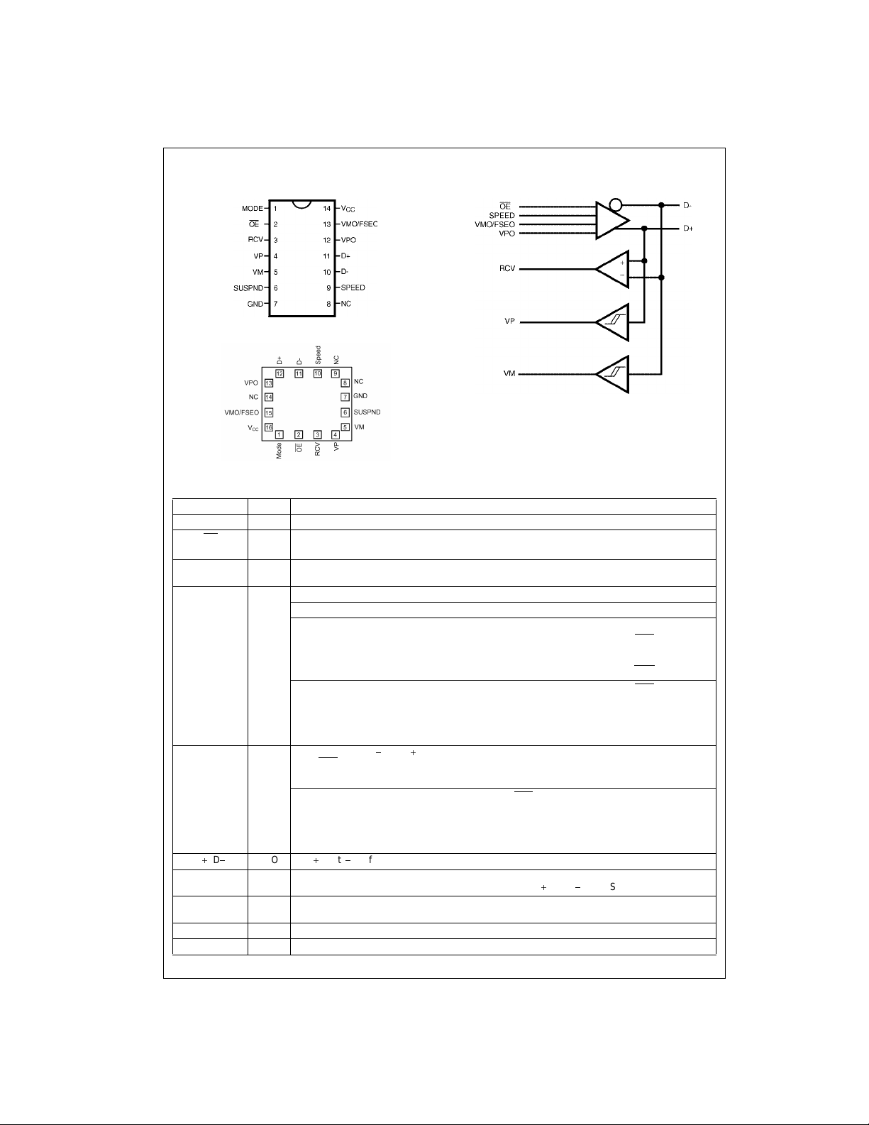
Connection Diagrams
Pin Assignments for SOIC and TSSOP
Logic Diagram
USB1T11A
Pin Assignments for MLP
Pin Descriptions
Pin Name I/O Description
RCV O Receive data. CMOS level output for US B differen tial input
OE
MODE I Mode. When left unconnected, a weak pull-up transistor pulls it to V
, VMO/F
V
PO
, V
V
P
M
, D
D
SUSPND I Suspend. Enables a low power state while the USB bus is inactive. While the suspend pin is
SPEED I Edge rate control. Logic “1” operates at edge rates for “full speed”.
V
CC
GND Ground reference
I Output Enable. Active LOW, enables the transceiver to transmit data on the bus. When not
active the transceiver is in receive mode.
and in this GND, the
VMO/FSEO pin takes the function of FSEO (Force SEO).
I Inputs to differential driver. (Outputs from SIE).
SEO
O Gated versi on of D and D. Outputs are logic “0” and logic “1”. Used to detect single ended
AI/O Data, Data. Differential data bus conforming to the Universal Serial Bus standard.
MODE VPO VMO/FSEO RESULT
0 0 0 Logic “0”
0 1 SE0
1 0 Logic “1”
11 SEO
1 0 0 SE0
0 1 Logic “0”
1 0 Logic “1”
1 1 Illegal code
zero (SE0
active it will drive the RCV pin to a logic “0” state. Both D
Logic “0” operates edge rates for “low speed”.
3.0V to 3.6V power supply
), error conditions, and interconnect speed. (Input to SIE).
VP VM RESULT
0 0 SE0
01Low Speed
1 0 Full Speed
11Error
CC
and D are 3-STATE.
www.fairchildsemi.com 2
Page 3
Functional Truth Table
Input I/O Outputs
Mode VPO VMO/FSEO OE
SUSPND D
D
RCV
V
0 0 0 0 0 0 1 0 0 1 Logic 0
0 0 1 0 0 0 0 U 0 0 SEO
0 1 0 0 0 1 0 1 1 0 Logic 1
0 1 1 0 0 0 0 U 0 0 SEO
1 0 0 0 0 0 0 U 0 0 SEO
1 0 1 0 0 0 1 0 0 1 Logic 0
1 1 0 0 0 1 0 1 1 0 Logic 1
1 1 1 0 0 1 1 U U U Illegal Code
XX X 10ZZUUUD
XX X 11ZZUUUD
X Don’t Care
Z
3-STATE
Undefined State
U
V
P
M
Result
/D
/D
USB1T11A
Hi-Z
Hi-Z
3 www.fairchildsemi.com
Page 4
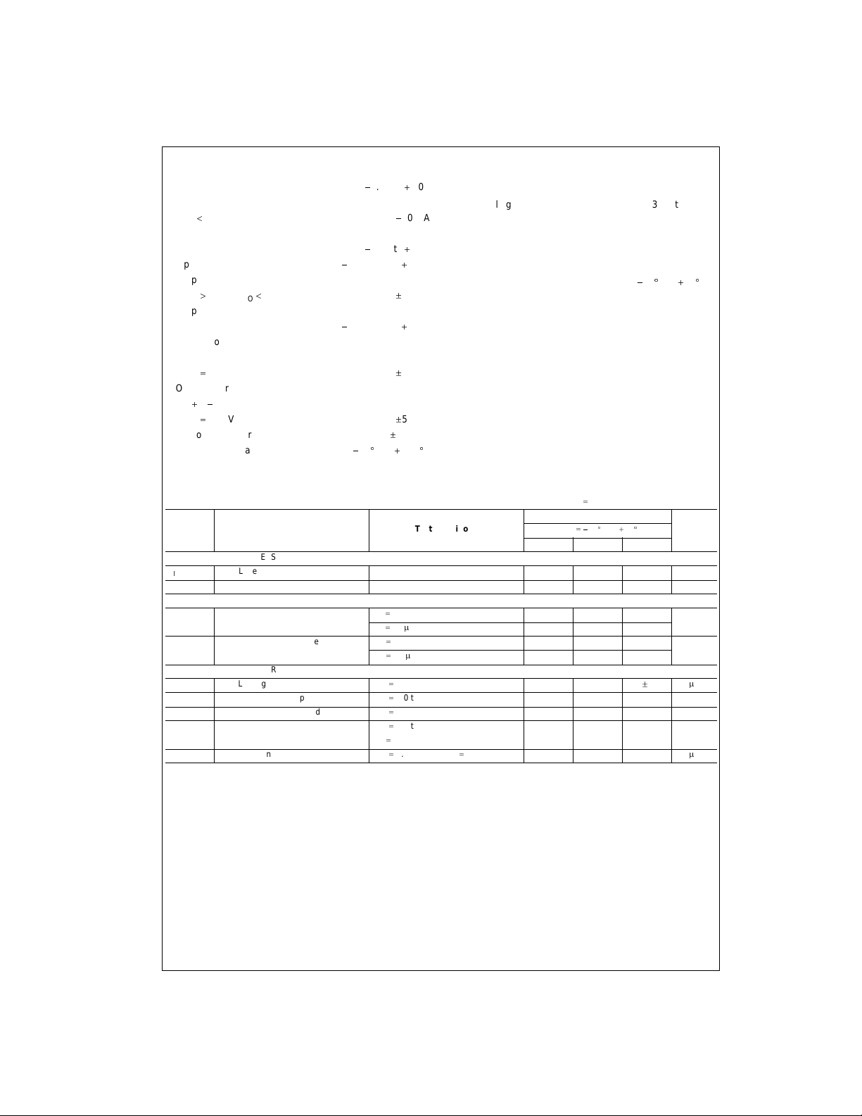
Absolute Maximum Ratings(Note 3) Recommended Operating
DC Supply Voltage (VCC)
DC Input Diode Current (I
V
0
USB1T11A
I
Input Voltage (V
)
I
(Note 4)
Input Voltage (V
)
I/O
Output Diode Current (I
! VCC or VO 0
V
O
Output Voltage (V
O
(Note 4)
Output Source or Sink Current (I
VP.VM, RCV pins
0 to V
V
O
CC
Output Source or Sink Current (I
D
/D
pins
0 to V
V
O
V
CC
CC
or GND Current (ICC, I
Storage Temperature (T
0.5V to 7.0V
)
OK
IK
0.5V to VCC 0.5V
)
50 mA
0.5V to 5.5V
r
50 mA
)
0.5V to VCC 0.5V
)
O
r
15 mA
)
O
r
50 mA
STO
GND
)
)
60q
C to 150qC
r
100 mA
Conditions
Supply Voltage V
Input Voltage (V
Input Range for AI/O (V
Output Voltage (VO) 0V to V
Operating Ambient Temperature
in free air (T
Note 3: The Absolute Maximum Ratings are those values beyond which
the safety of the d evice cannot be guaranteed. The device sh ould not be
operated at these limi ts. The parametric values define d in the Electrical
Characteristic tables are not gua ranteed at the absolute ma ximum rating .
The “Recomme nded O peratin g Cond itions ” table w ill def ine th e cond itions
for actual device operation.
Note 4: The input and o utp ut vol tage r ati ngs ma y be ex ceed ed if th e inpu t
and output clamp c urrent ratings are observ ed.
CC
)0V to 5.5V
I
amb
) 0V to V
AI/O
)
DC Electrical Characteristics (Digital Pins)
Over recommended range of supply voltage and operating free air temperature (unless otherwise noted). VCC 3.0V to 3.6V
Symbol Parameter Test Conditions
Min Typ Max
CC
V
V
V
V
I
L
I
CCFS
I
CCLS
I
CCQ
I
CCS
INPUT LEVELS:
IL
IH
OL
OH
LOW Level Input Voltage 0.8 V
HIGH Level Input Voltage 2.0 V
OUTPUT LEVELS:
LOW Level Output Voltage IOL 4 mA 0.4
HIGH Level Output Voltage IOH 4 mA 2.4
LEAKAGE CURRENT:
Input Leakage Current VCC 3.0 to 3.6
Supply Current (Full Speed) VCC 3.0 to 3.6 5 mA
Supply Current (Low Speed) VCC 3.0 to 3.6 5 mA
Quiescent Current VCC 3.0 to 3.6
Supply Current in Suspend VCC 3.0 to 3.6; Mode V
IOL 20 PA0.1
20 PAV
I
OH
VIN VCC or GND
CC
Limits
– 0.1
3.0V to 3.6V
CC
CC
40q
C to 85qC
UnitTemp 40qC to 85qC
V
V
r
5
P
A
5mA
10
P
A
www.fairchildsemi.com 4
Page 5

DC Electrical Characteristics (D
/D
Pins)
Over recommended range of supply voltage and operating free air temperature (unless otherwise noted). VCC 3.0V to 3.6V
Limits
Symbol Parameter Test Conditions
UnitsTemp 40qC to 85qC
Min Typ Max
INPUT LEVELS:
V
DI
V
CM
V
SE
Differential Input Sensitivity |(D) – (D)| 0.2 V
Differential Common Mode Range Includes VDI Range 0.8 2.5 V
Single Ended Receiver Threshold 0.8 2.0 V
OUTPUT LEVELS:
V
OL
V
OH
V
CR
Static Output LOW Voltage RL of 1.5 k: to 3.6V 0.3 V
Static Output HIGH Voltage RL of 15 k: to GND 2.8 3.6 V
Differential Crossover 1.3 2.0 V
LEAKAGE CURRENT:
I
OZ
High Z State Dat a Li ne Le akage Cur ren t 0V VIN 3.3V
r
5
CAPACITANCE:
CIN(Note 6) Transceiver Capacitance Pin to GND 10 pF
Capacitance Match 10 %
OUTPUT RESISTANCE:
Z
(Note 5) Driver Output Resistance Steady State Drive 4 20
DRV
Resistance Match 10 %
Note 5: Excludes external resistor. In order to comply with USB Specification 1.1, external series resistors of 24: r 1% each on D and D are recom-
mended. This sp ecificatio n is guaranteed by design and stat istical proc es s distribution.
Note 6: This spec ification i s guaranteed by design and statis t ical process distribution.
USB1T11A
P
A
:
AC Electrical Characteristics (D
/D
Pins, Full Speed)
Over recommended range of supply voltage and operating free air temperature (unless otherwise noted). V
50 pF; RL 1.5 k: on D to V
C
L
CC
Symbol Parameter Test Condition
Min Typ Max
DRIVER CHARACTERISTICS:
10% and 90% ns
t
t
t
V
R
F
RFM
CRS
Rise Time Figure 1 4 20
Fall Time Figure 1 4 20
Rise/Fall Time Matching (tr/tf)90110%
Output Signal Crossover Voltage 1.3 2.0 V
DRIVER TIMINGS:
t
PLH
t
PLH
t
PHZ
t
PLZ
t
PZH
t
PZL
Driver Propagation Delay Figure 2 18 ns
(VPO, VMO/FSEO to D/D) Figure 2 18ns
Driver Disable Delay Figure 4 13 ns
(OE to D/D) Figure 4 13ns
Driver Enable Delay Figure 4 17 ns
(OE to D/D) Figure 4 17ns
RECEIVER TIMINGS:
t
PLH
t
PHL
t
PLH
t
PHL
Receiver Propagation Delay Figure 3 16 ns
(D, D to RCV) Figure 3 19 ns
Single-ended Receiver Delay Figure 3 8 ns
(D, D to VP, VM) Figure 3 8 ns
3.0V to 3.6V
CC
Limits
UnitsTemp 40qC to 85qC
5 www.fairchildsemi.com
Page 6

AC Electrical Characteristics (D
/D
Pins, Low Speed)
Over recommended range of supply voltage and operating free air temperature (unless otherwise noted). V
200 pF to 600 pF; RL 1.5k: on D to V
C
L
Symbol Parameter Test Conditions
USB1T11A
CC
Min Typ Max
DRIVER CHARACTERISTICS:
10% and 90%
t
t
V
LR
LF
RFM
CRS
Rise Time Figure 1 75 300
Fall Time Figure 1 75 300
Rise/Fall Time Matching (tr/tf) 80 120 %
Output Signal Crossover Voltage 1.3 2.0 V
DRIVER TIMINGS:
t
PLH
t
PHL
t
PHZ
t
PLZ
t
PZH
t
PZL
Driver Propagation Delay Figure 2 300 ns
(VPO, VMO/FSEO to D/D) Figure 2 300 ns
Driver Disable Delay Figure 4 13 ns
(OE to D/D) Figure 4 13ns
Driver Enable Delay Figure 4 205 ns
(OE to D/D) Figure 4 205 ns
RECEIVER TIMINGS:
t
PLH
t
PHL
t
PLH
t
PHL
Receiver Propagation Delay Figure 3 18 ns
(D, D to RCV) F igure 3 18 ns
Single-ended Receiver Delay Figure 3 28 ns
(D, D to VP, VM) Figure 3 28 ns
CC
Limits
T
40qC to 85qC
amb
3.0V to 3.6V
Unit
nst
www.fairchildsemi.com 6
Page 7

AC Waveforms
VOL and VOH are the typical output voltage drops that occur with the output load. (VCC never goes below 3.0V)
USB1T11A
FIGURE 1. Rise and Fall Times FIGURE 2. VPI, VMO/FSEO to D
FIGURE 3. D/D to RCV, VP/VM
Test Circuits and Waveforms
Load for VM/VP and RCV
Note:
0 for t
V
V VCC for t
FIGURE 4. OE
to D/D
Load for Enable and Disable Times
, t
PZH
PHZ
, t
PZL
PLZ
/D
Load for D/D
Test S1
C
50 pF, Full Speed D/LS Close
L
C
200 pF, Low Speed (Min Timing) D/LS Open
L
600 pF, Low Speed (Max Timing) D/FS Open
C
L
1.5 k
:
on D (Low Speed) or D (Full Speed) only D/FS Close
7 www.fairchildsemi.com
Page 8

Tape and Reel Specification
Tape Format for MLP
Package Tape Number Cavity Cover Tape
Designator Section Cavities Status Status
USB1T11A
BQX Carrier 2500 Filled Sealed
TAPE DIMENSIONS inches (millimeters)
Leader (Start End) 125 (typ) Empty Sealed
Trailer (Hub End) 75 (typ) Empty Sealed
REEL DIMENSIONS inches (millimeters)
Tape Size
12 mm 330 178 12.4 18.4
www.fairchildsemi.com 8
A
(mm)
(Typical)
(mm)
N
W1
(mm)
W2
(Max)
(mm)
Page 9

Physical Dimensions inches (millimeters) unless otherwise noted
USB1T11A
14-Lead Small Outline Integrated Circuit (SOIC), JEDEC MS-012, 0.150" Narrow
Package Number M14A
9 www.fairchildsemi.com
Page 10

Physical Dimensions inches (millimeters) unless otherwise noted (Continued)
USB1T11A
Pb-Free 16-Terminal Molded Leadless Package (MLP), JEDEC MO-220, 3mm square
www.fairchildsemi.com 10
Package Number MLP16C
Page 11

Physical Dimensions inches (millimeters) unless otherwise noted (Continued)
Physical Dimensions inches (millimeters) unless otherwise noted (Continued)
USB1T11A Universal Serial Bus Transceiver
14-Lead Thin Shrin k Small Ou tlin e Pack age (TSSOP), JEDEC MO-153, 4.4mm Wide
Fairchild does not assume any responsibility for use of any circ uitry described, no circuit patent licenses are implied and
Fairchild reserves the right at any time without notice to change said circuitry and specifications.
LIFE SUPPORT POLICY
FAIRCHILD’S PRODUCTS ARE NOT AUTHORIZED FOR USE AS CRITICAL COMPONENTS IN LIFE SUPPORT
DEVICES OR SYSTEMS WITHOUT THE EXPRESS WRITTEN APPROVAL OF THE PRESIDENT OF FAIRCHILD
SEMICONDUCTOR CORPORATION. As used herein:
1. Life sup por t de vices o r syst ems are dev ices or syste ms
which, (a) are intended for surgical implant into the
body, or (b) support or sustain life, and (c) whose failure
to perform when properly used in accordance with
instructions for use provide d in the l abe ling, can be reasonably expected to result in a significant injury to the
user.
Package Number MTC14
2. A criti cal com ponen t in any com ponen t of a life s uppor t
device or system whose failure to perform can be reasonably expected to cause the failure of the life support
device or system, or to affect its safety or effectiveness.
www.fairchildsemi.com
11 www.fairchildsemi.com
 Loading...